CN100407054C - Lithographic apparatus and device manufacturing method - Google Patents
Lithographic apparatus and device manufacturing method Download PDFInfo
- Publication number
- CN100407054C CN100407054C CN2004100714648A CN200410071464A CN100407054C CN 100407054 C CN100407054 C CN 100407054C CN 2004100714648 A CN2004100714648 A CN 2004100714648A CN 200410071464 A CN200410071464 A CN 200410071464A CN 100407054 C CN100407054 C CN 100407054C
- Authority
- CN
- China
- Prior art keywords
- substrate
- pattern
- detecting device
- lithographic equipment
- suprabasil
- Prior art date
- Legal status (The legal status is an assumption and is not a legal conclusion. Google has not performed a legal analysis and makes no representation as to the accuracy of the status listed.)
- Active
Links
- 238000004519 manufacturing process Methods 0.000 title description 7
- 239000000758 substrate Substances 0.000 claims abstract description 218
- 230000003287 optical effect Effects 0.000 claims description 44
- 230000005855 radiation Effects 0.000 claims description 31
- 238000007689 inspection Methods 0.000 claims description 16
- 238000000059 patterning Methods 0.000 claims description 16
- 238000000034 method Methods 0.000 claims description 14
- 230000015572 biosynthetic process Effects 0.000 claims description 9
- 238000003491 array Methods 0.000 claims description 6
- 230000000875 corresponding effect Effects 0.000 description 9
- 230000003252 repetitive effect Effects 0.000 description 5
- 238000005516 engineering process Methods 0.000 description 4
- 230000002349 favourable effect Effects 0.000 description 4
- 238000003384 imaging method Methods 0.000 description 4
- 239000007788 liquid Substances 0.000 description 4
- 238000005259 measurement Methods 0.000 description 4
- 238000012937 correction Methods 0.000 description 3
- 238000009826 distribution Methods 0.000 description 3
- 238000007654 immersion Methods 0.000 description 3
- 239000000463 material Substances 0.000 description 3
- 238000001259 photo etching Methods 0.000 description 3
- 238000012545 processing Methods 0.000 description 3
- XUIMIQQOPSSXEZ-UHFFFAOYSA-N Silicon Chemical compound [Si] XUIMIQQOPSSXEZ-UHFFFAOYSA-N 0.000 description 2
- 230000005540 biological transmission Effects 0.000 description 2
- 238000001914 filtration Methods 0.000 description 2
- 239000011521 glass Substances 0.000 description 2
- 238000010438 heat treatment Methods 0.000 description 2
- 230000004807 localization Effects 0.000 description 2
- 239000003550 marker Substances 0.000 description 2
- 238000012544 monitoring process Methods 0.000 description 2
- 238000005457 optimization Methods 0.000 description 2
- 230000004044 response Effects 0.000 description 2
- 238000000926 separation method Methods 0.000 description 2
- 229910052710 silicon Inorganic materials 0.000 description 2
- 239000010703 silicon Substances 0.000 description 2
- 230000003068 static effect Effects 0.000 description 2
- 239000010409 thin film Substances 0.000 description 2
- 238000000429 assembly Methods 0.000 description 1
- 230000000712 assembly Effects 0.000 description 1
- 238000001816 cooling Methods 0.000 description 1
- 230000002596 correlated effect Effects 0.000 description 1
- 230000002950 deficient Effects 0.000 description 1
- 238000001514 detection method Methods 0.000 description 1
- 238000010586 diagram Methods 0.000 description 1
- 235000013399 edible fruits Nutrition 0.000 description 1
- 230000005670 electromagnetic radiation Effects 0.000 description 1
- 238000010894 electron beam technology Methods 0.000 description 1
- 238000007687 exposure technique Methods 0.000 description 1
- 210000003128 head Anatomy 0.000 description 1
- 238000005286 illumination Methods 0.000 description 1
- 238000009434 installation Methods 0.000 description 1
- 238000010884 ion-beam technique Methods 0.000 description 1
- 230000005381 magnetic domain Effects 0.000 description 1
- 238000012423 maintenance Methods 0.000 description 1
- 239000011159 matrix material Substances 0.000 description 1
- QSHDDOUJBYECFT-UHFFFAOYSA-N mercury Chemical group [Hg] QSHDDOUJBYECFT-UHFFFAOYSA-N 0.000 description 1
- 229910052753 mercury Inorganic materials 0.000 description 1
- 239000000203 mixture Substances 0.000 description 1
- 239000002245 particle Substances 0.000 description 1
- 230000002093 peripheral effect Effects 0.000 description 1
- 238000002360 preparation method Methods 0.000 description 1
- 210000001747 pupil Anatomy 0.000 description 1
- 230000011514 reflex Effects 0.000 description 1
- 230000001105 regulatory effect Effects 0.000 description 1
- 238000007493 shaping process Methods 0.000 description 1
- 238000004088 simulation Methods 0.000 description 1
- 239000005361 soda-lime glass Substances 0.000 description 1
- 230000001360 synchronised effect Effects 0.000 description 1
- XLYOFNOQVPJJNP-UHFFFAOYSA-N water Substances O XLYOFNOQVPJJNP-UHFFFAOYSA-N 0.000 description 1
Images


Classifications
-
- G—PHYSICS
- G03—PHOTOGRAPHY; CINEMATOGRAPHY; ANALOGOUS TECHNIQUES USING WAVES OTHER THAN OPTICAL WAVES; ELECTROGRAPHY; HOLOGRAPHY
- G03F—PHOTOMECHANICAL PRODUCTION OF TEXTURED OR PATTERNED SURFACES, e.g. FOR PRINTING, FOR PROCESSING OF SEMICONDUCTOR DEVICES; MATERIALS THEREFOR; ORIGINALS THEREFOR; APPARATUS SPECIALLY ADAPTED THEREFOR
- G03F9/00—Registration or positioning of originals, masks, frames, photographic sheets or textured or patterned surfaces, e.g. automatically
- G03F9/70—Registration or positioning of originals, masks, frames, photographic sheets or textured or patterned surfaces, e.g. automatically for microlithography
- G03F9/7088—Alignment mark detection, e.g. TTR, TTL, off-axis detection, array detector, video detection
-
- G—PHYSICS
- G03—PHOTOGRAPHY; CINEMATOGRAPHY; ANALOGOUS TECHNIQUES USING WAVES OTHER THAN OPTICAL WAVES; ELECTROGRAPHY; HOLOGRAPHY
- G03B—APPARATUS OR ARRANGEMENTS FOR TAKING PHOTOGRAPHS OR FOR PROJECTING OR VIEWING THEM; APPARATUS OR ARRANGEMENTS EMPLOYING ANALOGOUS TECHNIQUES USING WAVES OTHER THAN OPTICAL WAVES; ACCESSORIES THEREFOR
- G03B27/00—Photographic printing apparatus
- G03B27/32—Projection printing apparatus, e.g. enlarger, copying camera
- G03B27/52—Details
- G03B27/53—Automatic registration or positioning of originals with respect to each other or the photosensitive layer
-
- G—PHYSICS
- G03—PHOTOGRAPHY; CINEMATOGRAPHY; ANALOGOUS TECHNIQUES USING WAVES OTHER THAN OPTICAL WAVES; ELECTROGRAPHY; HOLOGRAPHY
- G03F—PHOTOMECHANICAL PRODUCTION OF TEXTURED OR PATTERNED SURFACES, e.g. FOR PRINTING, FOR PROCESSING OF SEMICONDUCTOR DEVICES; MATERIALS THEREFOR; ORIGINALS THEREFOR; APPARATUS SPECIALLY ADAPTED THEREFOR
- G03F7/00—Photomechanical, e.g. photolithographic, production of textured or patterned surfaces, e.g. printing surfaces; Materials therefor, e.g. comprising photoresists; Apparatus specially adapted therefor
- G03F7/70—Microphotolithographic exposure; Apparatus therefor
- G03F7/70216—Mask projection systems
- G03F7/70283—Mask effects on the imaging process
- G03F7/70291—Addressable masks, e.g. spatial light modulators [SLMs], digital micro-mirror devices [DMDs] or liquid crystal display [LCD] patterning devices
-
- G—PHYSICS
- G03—PHOTOGRAPHY; CINEMATOGRAPHY; ANALOGOUS TECHNIQUES USING WAVES OTHER THAN OPTICAL WAVES; ELECTROGRAPHY; HOLOGRAPHY
- G03F—PHOTOMECHANICAL PRODUCTION OF TEXTURED OR PATTERNED SURFACES, e.g. FOR PRINTING, FOR PROCESSING OF SEMICONDUCTOR DEVICES; MATERIALS THEREFOR; ORIGINALS THEREFOR; APPARATUS SPECIALLY ADAPTED THEREFOR
- G03F7/00—Photomechanical, e.g. photolithographic, production of textured or patterned surfaces, e.g. printing surfaces; Materials therefor, e.g. comprising photoresists; Apparatus specially adapted therefor
- G03F7/70—Microphotolithographic exposure; Apparatus therefor
- G03F7/70691—Handling of masks or workpieces
- G03F7/70716—Stages
-
- G—PHYSICS
- G03—PHOTOGRAPHY; CINEMATOGRAPHY; ANALOGOUS TECHNIQUES USING WAVES OTHER THAN OPTICAL WAVES; ELECTROGRAPHY; HOLOGRAPHY
- G03F—PHOTOMECHANICAL PRODUCTION OF TEXTURED OR PATTERNED SURFACES, e.g. FOR PRINTING, FOR PROCESSING OF SEMICONDUCTOR DEVICES; MATERIALS THEREFOR; ORIGINALS THEREFOR; APPARATUS SPECIALLY ADAPTED THEREFOR
- G03F7/00—Photomechanical, e.g. photolithographic, production of textured or patterned surfaces, e.g. printing surfaces; Materials therefor, e.g. comprising photoresists; Apparatus specially adapted therefor
- G03F7/70—Microphotolithographic exposure; Apparatus therefor
- G03F7/70691—Handling of masks or workpieces
- G03F7/70791—Large workpieces, e.g. glass substrates for flat panel displays or solar panels
-
- G—PHYSICS
- G03—PHOTOGRAPHY; CINEMATOGRAPHY; ANALOGOUS TECHNIQUES USING WAVES OTHER THAN OPTICAL WAVES; ELECTROGRAPHY; HOLOGRAPHY
- G03F—PHOTOMECHANICAL PRODUCTION OF TEXTURED OR PATTERNED SURFACES, e.g. FOR PRINTING, FOR PROCESSING OF SEMICONDUCTOR DEVICES; MATERIALS THEREFOR; ORIGINALS THEREFOR; APPARATUS SPECIALLY ADAPTED THEREFOR
- G03F9/00—Registration or positioning of originals, masks, frames, photographic sheets or textured or patterned surfaces, e.g. automatically
- G03F9/70—Registration or positioning of originals, masks, frames, photographic sheets or textured or patterned surfaces, e.g. automatically for microlithography
- G03F9/7003—Alignment type or strategy, e.g. leveling, global alignment
- G03F9/7023—Aligning or positioning in direction perpendicular to substrate surface
- G03F9/7026—Focusing
-
- G—PHYSICS
- G03—PHOTOGRAPHY; CINEMATOGRAPHY; ANALOGOUS TECHNIQUES USING WAVES OTHER THAN OPTICAL WAVES; ELECTROGRAPHY; HOLOGRAPHY
- G03F—PHOTOMECHANICAL PRODUCTION OF TEXTURED OR PATTERNED SURFACES, e.g. FOR PRINTING, FOR PROCESSING OF SEMICONDUCTOR DEVICES; MATERIALS THEREFOR; ORIGINALS THEREFOR; APPARATUS SPECIALLY ADAPTED THEREFOR
- G03F9/00—Registration or positioning of originals, masks, frames, photographic sheets or textured or patterned surfaces, e.g. automatically
- G03F9/70—Registration or positioning of originals, masks, frames, photographic sheets or textured or patterned surfaces, e.g. automatically for microlithography
- G03F9/7073—Alignment marks and their environment
Abstract
A lithographic apparatus in which alignment marks on the substrate are inspected during the exposure of the substrate to optimize the exposure conditions.
Description
Technical field
The present invention relates to lithographic equipment and device making method.
Background technology
Lithographic equipment is the equipment that required pattern is applied to base target portion.Lithographic equipment for example can be used for integrated circuit (ICs), flat-panel monitor and other comprise the manufacturing of the device of fine structure.In traditional lithographic equipment; patterning device; perhaps be called mask or graticule; can be used for producing the circuit pattern corresponding to IC (or other devices) individual layer, this pattern can be imaged in the target portion of the substrate (for example silicon chip or glass plate) with radiation-sensitive materials (resist) layer (for example comprising part, one or some circuit small pieces (die)).Replace mask, patterning device can comprise the independent controllable component array that is used for producing circuit pattern.
Generally, single substrate will comprise the grid of the adjacent target portion of exposure in succession.Known lithographic equipment comprises so-called ledex, wherein by whole pattern single exposure is shone each target portion in target portion, with so-called scanner, wherein pass through at projecting beam lower edge assigned direction (" scanning " direction) scan pattern, simultaneously along shining each target portion with the parallel or antiparallel direction synchronous scanning of this direction substrate.
In order to utilize photoetching technique to make device, the device that forms with the multilayer manufacturing generally is necessary.When this device made with multilayer, when forming for every layer, guarantee its with before layer to aim at be necessary.So known alignment mark that in substrate, provides.Every layer before exposure in the substrate, be sent to the aligning measuring center with every layer, wherein be provided with alignment mark, allow the accurate mensuration of substrate with respect to the position of alignment sensor.By with controlled manner substrate being moved to exposure position, but application site is proofreaied and correct with the tram in substrate and is accurately produced thereafter layer.Reduce aliasing error in the time of can using such system to guarantee to compare with critical feature size.
Yet,, therefore require overlapping accuracy further to improve because critical feature size reduces continuously.In addition, because alignment request is increased, therefore location and the inspection time that alignment mark spent increase, and the turnout of device reduces.
Summary of the invention
An object of the present invention is to provide a kind of method and apparatus, wherein, overlapping accuracy can improve and the turnout that installs does not significantly reduce.
For this reason, the invention provides a kind of lithographic equipment, comprising: illuminator provides the radiation projecting beam; Patterning device is used for making projecting beam to have pattern in its xsect; Base station is used for support base; Optical projection system is the target portion of the light beam projecting that forms pattern to this substrate; Detecting device is positioned at the light beam projecting that this optical projection system will form pattern in this substrate and checks substrate in the position of this substrate; Controller responds from the following at least parameter of the information adjustment of this detecting device: be projected to this suprabasil pattern position of this substrate relatively; Be projected to the magnification of this suprabasil pattern; Resemble face with optimum focusing; Wherein, this detecting device has a plurality of sensors, is used for checking simultaneously a plurality of base part across the whole width of this substrate; This patterning device and this optical projection system be arranged to expose whole width of this substrate, thus can this substrate relatively the single of this device by middle inspection and this substrate that exposes.
Therefore, the turnout of device can increase, because detecting device can be at single by the whole substrates of middle inspection, or represents the base part of whole substrate, and by with respect to described device scanning substrate, the required pattern of exposure in substrate.This is especially favourable in the manufacturing of for example flat-panel monitor, and wherein processed substrate of glass size can reach 2m * 2m or bigger.
Such device is favourable equally, because the overlapping accuracy of the every part of substrate can improve.In addition, because when substrate is positioned at exposure position, can check the some parts of substrate, therefore the process that substrate is moved to exposure position from the aligning measuring position, can not introduce error.Therefore, advantageously, the overlapping defective that not only can consider in treatment step before to introduce substrate, and can consider the change that between this layer exposure period, takes place.For example, this system can compensate between exposure period the substrate expansion that the heating by substrate causes, this heating is caused by every layer the radiation of being used to expose.Therefore, the overlapping accuracy of the every part of substrate improves.In addition, owing to do not need substrate is sent to independent aligning measuring center, so the processing time of substrate does not significantly increase.
In said apparatus, described detecting device inspection is by the functional character that treatment step produced, that be formed on this suprabasil device of front.Therefore, because the detecting device inspection is formed on the functional character of suprabasil device, less special aligned mark need be formed in the substrate, perhaps can eliminate fully for their needs.Therefore the major part of basal region can be used to form at suprabasil active device.
Preferably, by checking the part of substrate, detecting device can be determined the position and/or the direction of this part of substrate, and/or this part of substrate is with respect to the amount of the expansion of the reference state of substrate.Can use this information adjustment to be projected to the position of the pattern of substrate, the magnification and the optimum focusing that are projected to the pattern of substrate resemble face.
Detecting device can be fixed basically with respect to the position of optical projection system and be known, perhaps can provide position transducer to come the position of monitoring detector with respect to optical projection system.Therefore, a substrate part can be easily with respect to the understanding of the position of detecting device and is accurately converted the understanding of this part of substrate with respect to the position of optical projection system to.In addition, locating device can also be set, this locating device moves described substrate relative to this optical projection system and this detecting device, so that the zones of different of this substrate that exposes continuously, wherein this detector arrangement becomes before the exposure of the given area of this substrate to check this zone.
In preferred embodiments, substrate or is moved with respect to optical projection system and detecting device when continuous exposure is carried out between continuous exposure, to such an extent as to detecting device arranges that like this part of the substrate that detecting device detects subsequently becomes the target portion of the substrate that is exposed.Substrate is known from the relative position of detecting device and optical projection system with respect to the position that detecting device and optical projection system must move.Therefore, detecting device can substrate to this part of checking substrate before the certain portions exposure soon; When this part of substrate was just being exposed, conditions of exposure can be adjusted according to the optimization overlapping accuracy.
Easily, substrate can be moved with respect to optical projection system and detecting device with constant substantially speed during the process of multiexposure, multiple exposure or during continuous exposure.This has reduced requirement that substrate is repeated to quicken with respect to optical projection system and detecting device, thereby has reduced the power that must apply.Therefore, the timing that timing by changing exposure and/or change are arranged on the pattern on the independent controllable component array also is possible along being parallel to the position that the moving direction adjustment of substrate with respect to optical projection system and detecting device be projected to the pattern of substrate.
In addition, described patterning device comprises independent controllable component array.At this moment, be projected to the position of this suprabasil pattern by one of the following adjustment at least: adjust the timing that is arranged on the pattern on the described independent controllable component array, be arranged on the position of the pattern on the described independent controllable component array by the electronics adjustment.Also can be arranged on the magnification that pattern adjustment on the described independent controllable component array is projected to this suprabasil pattern by the electronics adjustment.
By physics mobile projector system, independent controllable component array patterning device, substrate or these combination and/or by moving the position of the pattern that on independent controllable component array, produces, can add or alternatively adjust the position of the pattern that is projected to substrate.
The present invention also can be applied to the device that is made of a plurality of independent controllable component arrays, wherein said element arrays be set to mutually away from.In this case, for one or more patterns that produced by independent controllable component array, controller can independently be adjusted the position of the pattern that is projected to substrate, and the magnification and/or the optimum focusing of pattern resemble face.This allows any mobile compensation between the single array of independent controllable component is also allowed for example inconsistent compensation of substrate deformation between the substrate zones of different is wherein projected to pattern in the substrate from each independent controllable component array.For this is become easily, detecting device can be checked the alignment mark in a plurality of positions of substrate simultaneously, and each alignment mark is corresponding to a suprabasil zone, and this substrate exposes simultaneously by a plurality of layout area able to programme.Can adjust the pattern that is projected to substrate here, expands with the localized heat that compensates for example substrate.Preferably, controller position and/or the optimum focusing that can further adjust the pattern that is projected to substrate resembles face.Be to be understood that the combination that also can use said structure.
In addition, the invention provides a kind of device making method, comprising: substrate is provided; Utilize illuminator that the radiation projecting beam is provided; Make this projecting beam in its xsect, have pattern with patterning device; The radiation laser beam that forms pattern is projected to the target portion of this substrate; This substrate be positioned at this optical projection system with the light beam projecting of described formation pattern in the position of this substrate, utilize detecting device to check the part of described substrate; Response is from the following at least parameter of the information adjustment of this detecting device: be projected to this suprabasil pattern position of this substrate relatively, the magnification and the optimum focusing that are projected to this suprabasil pattern resemble face; Wherein, this detecting device has a plurality of sensors, is used for checking simultaneously a plurality of base part across the whole width of this substrate, this patterning device and this optical projection system be arranged to expose whole width of this substrate; This method further be included in this substrate relatively the single of this lithographic equipment by this substrate of middle inspection and expose at this suprabasil pattern.
In above-mentioned device making method, described detecting device is checked the functional character that treatment step produced, that be formed on this suprabasil device of front.
Term used herein " controllable component array separately " should broadly be interpreted as relating to gives any parts in patterned cross section can for the radiation laser beam of incident, so that required pattern can be created in the target portion of substrate; Also use term " light valve " and " spatial light modulator " herein (SLM).The example of this patterning device comprises:
-array of programmable mirrors.This can comprise matrix-addressable surface, and it has a viscoelasticity key-course and a reflecting surface.The theoretical foundation of this device is that the addressed areas of (for example) reflecting surface reflects incident light as diffraction light, but not addressed areas reflects incident light as non-diffracted light.With a suitable spatial light filter, the described non-diffracted light of filtering from beam reflected only keeps diffraction light and arrives substrate; In this manner, light beam produces pattern according to the addressing pattern of matrix-addressable surface.Should be appreciated that as a kind of selection light filter can the filtering diffraction light, keep non-diffracted light and arrive substrate.Diffraction optics MEMS device array also can be used for corresponding mode.Each diffraction optics MEMS device is made of a plurality of zones of reflections, and a plurality of zones of reflections can be out of shape toward each other to form grating, and this grating reflects incident light as diffraction light.Another embodiment of array of programmable mirrors is utilized the arranged of tiny mirror, by using suitable internal field, perhaps by using piezoelectric actuator device, makes that each catoptron can be independently about an inclination.Moreover catoptron is a matrix-addressable, and addressed mirrors reflexes on the non-addressed mirrors with the radiation laser beam of different directions with incident thus; In this manner, the addressing pattern according to the matrix-addressable catoptron carries out composition to folded light beam.Can carry out this required matrix addressing with suitable electronic installation.In above-mentioned two kinds of situations, the controllable component array can comprise one or more array of programmable mirrors separately.The more information of the reflection mirror array that relates to here can obtain from for example U.S. Pat 5,296,891 and US 5,523,193 and PCT patented claim WO 98/38597 and WO 98/33096, and these documents here are incorporated herein by reference.
-Programmable LCD array.For example by U.S. Pat 5,229, the 872 this structures that provide, it here is incorporated herein by reference.
Be to be understood that, use for example prebias feature, optics near the place of revising feature, phase change technology and multiple exposure technique, " demonstration " pattern can be different from layer or the suprabasil pattern of finally transferring to substrate in fact on independent controllable component array.Similarly, finally being created in suprabasil pattern can be inconsistent with the pattern that any one moment is formed on the independent controllable component array.May be this situation in the device, wherein form the final pattern that forms in given time cycle or given exposure frequency on each part of substrate, in the above-mentioned time, the pattern on controllable component array separately and/or the relative position of substrate change.
Although in this application, lithographic equipment specifically is used to make ICs, should be appreciated that lithographic equipment described herein may have other application.For example, the guiding and the check pattern of the manufacturing of integrated optics system, magnetic domain memory, flat-panel monitor, thin-film head etc.It will be apparent to one skilled in the art that in this interchangeable purposes scope any use of term " wafer " or " circuit small pieces " here should be thought respectively can be by more common term " substrate " or " target portion " replacement.Here the substrate that relates to can be before or after the exposure, handle in for example track (general resist layer is coated to substrate and a kind of instrument of the resist that exposed of developing) or tolerance, checking tool.The place that is suitable for, disclosure herein can be applied to these and other base treatment instruments.Further, processing substrate that can be more than once, for example in order to produce multilayer IC, therefore term substrate used herein also relate to comprised that multilayer handled layer substrate.
Term used herein " radiation " and " light beam " comprise all types of electromagnetic radiation, comprise that ultraviolet (UV) radiation (for example has 408,355,365,248,193,157 or the wavelength of 126nm) and extreme ultraviolet (EUV) radiation (wavelength coverage that for example has the 5-20nm scope), and the particle beams, as ion beam or electron beam.
Term used herein " optical projection system " should broadly be interpreted as comprising various types of optical projection systems, comprise dioptric system, reflective optics, and catadioptric optical systern, the exposing radiation that is suitable for for example using, perhaps the use of other factors such as immersion liquid or vacuum is suitable for.Here any use of term " camera lens " is thought and can be replaced by more common term " optical projection system ".
Illuminator also can comprise various types of optical elements, for example comprises reflecting, reflecting and reflexed is penetrated optical element, is used for guiding, shaping or control radiation projecting beam, and this parts also can jointly or individually be called " camera lens " hereinafter.
Lithographic equipment can be for having the type of two (twin-stages) or a plurality of base station.In this " multi-stag " device, can walk abreast and use these additional stations, perhaps can on one or more platform, carry out preparation process, and one or more other be used for exposure.
Lithographic equipment also can be wherein the type that has in relative high refractive index liquid, for example water to be immersed in substrate, so that this liquid is full of the final parts of optical projection system and the space between the substrate.Immersion liquid also can be applied to other spaces in the lithographic equipment, for example, and between first parts of independent controllable component array and optical projection system.The immersion technology is known in affiliated field, is used for increasing the numerical aperture of optical projection system.
Description of drawings
Describe embodiment of the present invention referring now to appended synoptic diagram, these embodiments are only as example, and wherein corresponding reference marker is represented corresponding part, wherein:
-Fig. 1 has described lithographic equipment according to one embodiment of the present invention;
-Fig. 2 a, 2b and 2c have described when suprabasil layer just is being exposed the substrate three time situations;
-Fig. 3 has described the exposing unit device that uses in device of the present invention;
-Fig. 4 has described the part of exposing unit illustrated in fig. 3;
-Fig. 5 has described the exposure area that produces by exposure system shown in Figure 3;
-Fig. 6 has described an example of the feature repetitive device that forms in substrate;
-Fig. 7 has described the detector cell device that uses in device of the present invention.
In the accompanying drawings, corresponding reference marker is represented corresponding part.
Embodiment
Fig. 1 has schematically shown the lithographic equipment of the present invention's one specific embodiments.This device comprises:
-illuminator (luminaire) IL is used to provide radiation projecting beam PB (for example UV radiation);
-independent controllable component array PPM (for example array of programmable mirrors) is used for pattern is applied to projecting beam; Generally, the position of controllable component array is fixed with respect to parts PL separately; Yet, also can replace with and it is connected with respect to the pinpoint locating device of parts PL;
-base station (for example wafer station) WT, support base W (for example applying the silicon wafer of resist), and be used for substrate is connected with respect to the pinpoint locating device PW of object PL; With
-projection system (" camera lens ") PL is imaged on pattern on the C of target portion (for example comprising one or more circuit small pieces) of substrate W, wherein makes projecting beam PB give this pattern by independent controllable component array PPM; Optical projection system can be with independent controllable component array image-forming in substrate; Perhaps, optical projection system can imaging second source, for the element of the independent controllable component array of this light source as optical gate; Optical projection system also can comprise focusing block array such as microlens array (being known as MLA) or array of fresnel lenses, for example to form second source and little point is imaged onto in the substrate.
As noted here, this device belongs to reflection-type (the independent controllable component array that promptly has reflection).Yet in general, it can also be a transmission-type (the independent controllable component array that promptly has transmission) for example.
Luminaire IL is from radiation source S O received radiation light beam.The source can be the material object that separates with lithographic equipment, for example when the source is excimer laser.In this case, do not think that the source is a part that forms lithographic equipment, radiation laser beam passes through from radiation source S O, and at the following arrival luminaire IL of assisting of beam delivery system BD, this transmission system comprises for example suitable directional mirror and/or optical beam expander.In other cases, the source can be the integral part of device, for example when the source is mercury lamp.Source SO and luminaire IL can be called radiating system with beam delivery system BD (if desired).
Luminaire IL can comprise regulating device AM, is used to adjust the angular intensity distribution of light beam.Usually, the outer at least and/or inside diameter ranges that can adjust the luminaire pupil plane (is called the intensity distributions of σ-outer and σ-Nei) usually.In addition, luminaire IL generally comprises various other assemblies, as integrator IN and condenser CO.Luminaire provides radiation to regulate light beam, is called projecting beam PB, has ideal uniform degree and intensity distributions in its xsect.
Light beam PB intersects with independent controllable component array PPM then.After controllable component array PPM reflected separately, light beam PB was by optical projection system PL, and it focuses on light beam PB on the C of target portion of substrate W.Assisting down of locating device PW (with interferometric measuring means IF), base station WT can accurately move, for example the different C of target portion in location in the light path of light beam PB.In use, for example in scan period, can use locating device accurately to proofread and correct the position of the relative light beam PB of independent controllable component array PPM light path for independent controllable component array.Generally, assisting down of long stroke module (coarse localization) that does not clearly show in Fig. 1 and short stroke module (accurately location) can realize moving of object table WT.Also can use similar system to locate independent controllable component array.Should be appreciated that projecting beam can be used as selection/additionally removable, when object table and/or separately the controllable component array have a fixing position so that required relatively moving to be provided.Select as another, this is particularly suitable in the manufacturing of flat-panel monitor, and promptly the position of base station and optical projection system can be fixed, and substrate can be arranged to move with respect to base station.For example, base station can be provided with scanning system, and this system scans substrate with constant substantially speed across substrate.
Although be described as resist on the exposed substrate here according to lithographic equipment of the present invention, should be appreciated that the present invention is not limited to this use, device can be used for the projecting beam that projection forms pattern, and this light beam is used to not have the photoetching process of resist.
Shown lithographic equipment can be used for four kinds of preference patterns:
1. step mode: the controllable component array makes projecting beam have whole pattern separately, this light beam by projection (being single static exposure) once to the C of target portion.Base station WT moves along X and/or Y direction then, so that the different C of target portion can expose.In step mode, the full-size of exposure area has limited the size of the C of target portion of imaging in single static exposure.
2. scan pattern: the controllable component array moves with speed v along given direction (so-called " direction of scanning, for example Y direction ") separately, so that projecting beam PB scans whole independent controllable component array; Simultaneously, base station WT moves with speed V=Mv simultaneously along identical or opposite direction, and wherein M is the magnification of camera lens PL.In scan pattern, the full-size of exposure area has limited the width (along non-direction of scanning) of the target portion in the exposure of single action attitude, and the length of scanning motion has determined the height (along the direction of scanning) of target portion.
3. pulse mode: the controllable component array keeps motionless substantially separately, utilizes impulse radiation source with the target portion C of whole graphic pattern projection to substrate.Base station WT moves with constant substantially speed and makes projecting beam PB scan the line across substrate W.Pattern on the controllable component array upgrades between the pulse of radiating system as requested separately, and pulse is that the C of target portion in succession that makes of timing exposes in the desired location of substrate.Therefore, projecting beam can be across the whole pattern of substrate W scanning with the bar of exposed substrate.Repeat these steps and pursued line exposing up to whole substrates.
4. continuous sweep pattern: basic identical with pulse mode, except utilizing constant substantially radiation source, the pattern on the controllable component array is along with projecting beam upgrades across substrate scanning and with its exposure separately.
Also can use combination and/or the variation or the diverse pattern of the pattern of above-mentioned use.
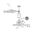
Fig. 2 a, 2b and 2c have illustrated according to device of the present invention.Exposure and alignment modules 15 are located at fixing position, and substrate 10 in its lower section is scanned.Fig. 2 a has described substrate and has arrived exposure and alignment modules 15 state before at once; Fig. 2 b has described the state that substrate begins to scan below exposure and alignment modules; Fig. 2 c has described the state of substrate continuation scanning below exposure and alignment modules 15.
Exposure and alignment modules 15 are made of detector cell 16 and exposing unit 17.Detector cell 16 is connected by infrastructural frame 18 with exposing unit 17, and this framework guarantees that the exposing unit 17 and the relative position of detector cell 16 fix.Infrastructural frame 18 can the material of low-thermal-expansion forms to guarantee relative position stable by having very.Can accurately determine relative position by calibration formerly then.When scanning substrate below exposure and alignment modules, the alignment mark that detector cell 16 is checked in the substrate 10.The information that is used to the self-check alignment mark in the direction of scanning, laterally (promptly in basal surface and) and accurately determine the position of substrate perpendicular to the direction of substrate perpendicular to the direction of scanning.In addition, can utilize alignment mark to determine the direction of substrate in all three angles of rotational freedom.Detector cell 16 checks that also alignment mark is to determine the degree of any thermal expansion of substrate.
Because substrate 10 is scanning below exposure and alignment modules 15, each part of substrate is at first below detector cell 16, then below exposing unit 17.Therefore, each part for substrate 10, linear position, direction and the expansion informations of being determined by detector cell 16 can be sent to exposing unit 17 when being exposed below exposing unit 17 with convenient substrate, and the conditions of exposure of this part of substrate can obtain optimization.Especially, in direction of scanning and site error transversely, can adjust the position of the pattern that is projected to this part of substrate for a substrate part; , can adjust optimum focusing and resemble face in site error for this part of substrate perpendicular to the base plane direction; And can carry out any thermal expansion that magnification correction is proofreaied and correct this part of substrate.In the device of for example making flat-panel monitor, detector cell 16 can be positioned at the place ahead 30cm (apart from the viewpoint of the substrate of advancing) of exposing unit 17.Substrate can be per second 50mm with respect to the sweep velocity of detector cell and exposing unit.Therefore device has 6 seconds time utilizing detector cell to check a substrate part and utilize between the exposing unit illumination same section.It is enough that this time will be adjusted exposure settings for the data that are used to the self-detector unit with basis in exposing unit.
Check the alignment mark of each part of substrate, allow to carry out continuous correction.Therefore, both made that aliasing error also can reduce when having the local deformation of substrate.In addition, the time difference between the pattern on inspection alignment mark and substrate and this part of exposed substrate is only by the spacing of detector cell 16 and exposing unit 17 and the sweep velocity restriction of substrate.This for the alignment mark substrate is at first scanned fully, is scanned with exposing patterns in known devices then fully with known devices is opposite at present.This causes having big time difference in give certain portions and this part of checking substrate for alignment mark between being exposed.During during this period of time, cause the additional deformation of aliasing error to be introduced into.For example, when substrate was exposed, the radiation that projects to substrate had increased the temperature of substrate.The increase of this temperature causes the thermal expansion of substrate.In known system, the thermal expansion between exposure period is not counted, and is separation steps because check alignment mark and exposure.Yet, in the present invention, count this expansion, because when exposure takes place, check alignment mark.This reaches the flat pannel display photoetching process particular importance of 2 meters long soda-lime glass plate for being used for imaging.For such plate, per 1 ℃ of temperature variation expands and is approximately 8 μ m.Therefore, between exposure period, do not check alignment mark for the overlapping accuracy that the 0 35 μ m that need are provided, the temperature of substrate entire plate need be controlled at ± and 0.05 ℃.This needs complicated heat control.
In addition, because the present invention does not require the separating treatment of checking suprabasil alignment mark, the processing time of every substrate reduces widely.
Suprabasil alignment mark can be: aim at grating, it is parallel to direction of scanning and horizontal; As the herringbone alignment mark that uses; Or by means of the image recognition of television imaging.The order of alignment mark can be arranged to be parallel to delegation or the multirow with respect to the direction of detector cell 16 scanning substrates, and is distributed on the whole length of substrate.The such alignment mark of preferred at least two row is located in the substrate.In each case, known being suitable for, use the detection optical system of alignment mark to be located in the detector cell 16.
In preferably being provided with, special-purpose alignment mark is not set in substrate.The substitute is, detector cell is provided with one or more sensors, and it can detect the characteristic pattern that forms in substrate in treatment step before.Such sensor can be the camera that is connected to controller, its middle controller service chart case recognizer.This set is favourable, because the special aligned mark is represented the part in suprabasil device feature of can not being used to form of substrate.Therefore, by using the feature of device itself, the major part of substrate can be used for the funtion part of device.This is particularly useful in the formation of for example flat-panel monitor, because the size of alignment mark is approximately identical with the size of a pixel of the display of formation.If therefore need alignment mark in display, this will cause lacking pixel in this position of resulting devices, and this obviously is unacceptable.The use that forms feature in layer before also is favourable, because when new layer just forms on the device in substrate, guarantees that itself and a layer covering correctly before the device that has formed are necessary.Be formed on the feature locations of the layer before suprabasil by direct measurement, the technician can guarantee down that one deck correctly covers.If, as described, the detector cell inspection replaces the functional character of the formation device of special aligned mark, around the edge that forms device, comprise that simulation feature (promptly presenting the feature similar to functional character) is necessary so, so that guarantee when the edge of device formation functional character, to aim at correct.
Fig. 6 has schematically represented to be formed on the part of suprabasil characteristic pattern during the manufacturing of flat-panel monitor.As shown in the figure, whole pattern is made of a plurality of repetitives 40, and each unit comprises control line 41, thin film transistor (TFT) 42 and pixel itself 43.Therefore image identification system can be used for discerning the repetitive and the position of measurement features accurately.Advantageously, can use the self study image identification system.As noted, pattern height can repeat.Therefore the image recognition detecting device can be used for the meticulous measurement of feature locations in the substrate, and piece-rate system can be used for rough location survey because there be not discernible difference on the substrate different piece between the repetitive.For example, scale can be located in the substrate, and promptly a series of mark is represented along the position of base length direction.For example an edge setting of scale along substrate.Because it is used to form the rough measure at the feature locations of suprabasil device.In other words, scale does not need to be formed on the following position of substrate, and this position is that to form the feature of the device that will form in substrate required.As selection, or additionally, canned data when scanning with respect to detector cell by substrate, image identification system can carry out coarse localization and measure.For example, detector cell can calculate and scan by detector cell, is formed on the number of repeating units of the pattern of suprabasil previous layer.Therefore this computational data can be used for determining which repetitive discerned by the pattern identification detecting device thereafter.
The position that is projected to the pattern of substrate can be moved by some modes.At first, when substrate 10 when exposure and alignment modules 15 times scan, can proofread and correct its position.For example, base station can be installed in provides on the mobile long stroke module of scanning; The short stroke mould is installed in soon between long stroke module and the base station and moves to provide to proofread and correct.Perhaps, exposure and alignment modules 15, perhaps exposing unit 17 (or its part) can be installed on the regulator at least, moves so that with the correction portion of graphic pattern projection to substrate to provide to proofread and correct.Further select is to move the pattern (promptly adjusting the data that are located on the independent controllable component array, so that pattern is occurring moving on the controllable component array separately) that is formed on the independent controllable component array electronically.If for example device is used for the continuous sweep pattern, then the timing that is set in the pattern on the independent controllable component array by timing or adjustment in the exposure of 17 times scanning of exposing unit substrate time control pattern can be parallel to the pattern position that the direction of scanning adjustment projects to substrate.Certainly, also can use the combination of above-mentioned technology.
Fig. 3 has described the detail drawing that is used for exposing unit 17 of the present invention.Exposing unit is made of a plurality of photo engines 21, and each can produce the radiation laser beam that forms pattern, and it is projected in the substrate 10.As shown in Figure 3, photo engine 21 is arranged to two arrays 22,23 perpendicular to the substrate direction of scanning.Fig. 4 shows the detail drawing of photo engine 21.Photo engine is by independent controllable component array 25, and projection optical system 26 and microlens array 27 constitute.Two or more photo engines 21 can be shared a public radiation source, and perhaps each is provided with independently radiation source.Although also should be appreciated that as shown in the figure, photo engine uses microlens array, and controllable component array 25 can wholely be imaged onto in the substrate 10 separately.
As shown in Figure 5, the array 22,23 of photo engine 21 produces the array 32,33 that generates corresponding pattern image 31 in substrate 10.In each array 22,23 of photo engine 21, be provided with between the photo engine at interval.This interval can be used for providing the space for photo engine provides assistant service as cooling or for radiation source.Therefore, in the array 32,33 of the picture 31 of the formation pattern that projects to substrate, there is the gap.Photo engine array 22, to such an extent as to 23 arrange like this substrate move one section give set a distance after, the gap as in first array 33 of 31 second array 32 and the picture of the formation pattern that projects to substrate by photo engine first array 23 of formation pattern that projects to substrate by photo engine second array 22 is consistent.Therefore, can expose across whole of horizontal substrate, although between photo engine 21, have the gap.As shown in Fig. 3 and 5, there are two arrays of photo engine 21.Yet should be appreciated that additional array can be located in the exposing unit 17, for example allow the bigger gap between the photo engine 21 or allow the exposure more than in single sweep operation, receiving once of each part of substrate.
In preferred embodiments, response can be carried out with each photo engine for each adjustment of the pattern that projects to substrate independently from the information of detector cell 16.This can be by providing independent regulator to control the position of each photo engine 21, by in the projection optical system 26 of each photo engine 21 and/or provide magnification control and optimum focusing image planes to control in microlens array, and/or the Data Control by separation is provided for each photo engine is so that applying electronic is proofreaied and correct and realized independently.By these modes, compensation is possible across the local distortion and the distortion of substrate.Yet wish that the compensation system (promptly influencing the compensation system of the pattern of all photo engines generations) that provides total equally compensates for example substrate site error generally.
Be not installed in the place of independent regulator at photo engine, the microlens array of all photo engines can be installed on the single infrastructural frame that preferably has a unusual low-thermal-expansion.Yet if desired, each microlens array is adjustable with respect to the position of infrastructural frame.Similarly, the independent controllable component array of all photo engines can be installed on the independent infrastructural frame, and each position with respect to infrastructural frame is adjustable.Therefore, can measure and calibrate the relative position of the pattern that produces by photo engine.
The magnification of each photo engine can be adjusted with any expansion of compensation substrate or by any other suitable optical means in position by changing independent controllable component array.As selecting or additionally,, can adjusting the magnification of the pattern that projects to substrate by changing the pattern that is applied to independent controllable component array with electronic device.As previously mentioned, this operation can be carried out independently and/or carries out (for example, by adjusting the position of the infrastructural frame that all independent controllable component arrays are installed on it) for all photo engine integral body for each photo engine.Preferably, the magnification range of control is ± 15ppm.
In the distortion of above-mentioned embodiment, detector cell 16 can strictly be connected to each other with exposing unit 17 or can be connected with the framework that is subject to thermal expansion.In this case, must be provided with position transducer with the position of monitoring exposing unit 17 with respect to detector cell 16.Even thereby, still know relative position if unfixing.
As shown in Figure 7, detector cell 16 is preferably by a plurality of sensor 16a, and 16b constitutes so that can be across the feature of whole width inspection alignment mark of substrate and/or the layer that had before formed in substrate.Therefore, when in exposing unit 17, conditions of exposure being set, can considering in the distortion of substrate across the variation of base widths and/or be formed on the aligning of suprabasil feature.As shown in Figure 7, sensor 16a in the detector cell 16,16b is with corresponding to the arrangement of photo engine in exposing unit 17.For example, sensor can be arranged to the first sensor array 16a and the second sensor array 16b, and each array comprises one group of sensor with spaced apart.Therefore, although check the whole width of substrate 10,, can the gap be set for control line, maintenance etc. around the 16b at each sensor 16a.
Should be appreciated that in aforesaid device each sensor 16a, 16b can arrange like this that the photo engine that i.e. utilization is correlated with exposes in succession by each part of the substrate of given sensor inspection so that relevant with a given photo engine 21.Should be appreciated that also this arrangement is not restricted to two line sensors as shown in Figure 7, can be configured to the row of any number as fruit instant.In addition, to such an extent as to detector cell 16 can be arranged each part that it does not check substrate 10 like this.For example, a line sensor can arrange across the width of detector cell 16, but be set to mutually away from.Therefore can be directly these regional conditions of exposures in the substrate be set from the measurement of sensor.For not by these zones between the zone of sensor inspection, can conditions of exposure be set by interpolative data from the sensor of two or more inspection substrate peripheral part.
Further be to be understood that, although above description of the present invention relates generally to the device that uses pulse mode (as mentioned above), wherein to move with constant substantially speed and expose be pulsed modulation in substrate, but should be appreciated that the present invention can similarly be applied to the device of step mode (as mentioned above) work and the device of working with scan pattern (as mentioned above).In addition, although the present invention relates to make radiation laser beam to form the use of the independent controllable component of pattern, should be appreciated that the present invention can similarly be applied to utilize the conventional fixed mask to make radiation laser beam form the device of pattern.In this case, for example can be used for the device with scan pattern work: detecting device can be between mask and substrate, and is arranged to be positioned at when scanning across substrate before the projecting beam that forms pattern.At last, although the invention describes the substrate of moving according to below exposure and aligned units, but understand easily, the absolute position of description is dispensable for the present invention, what the given partial fixing of device neither be necessary: it is necessary only having substrate to move with respect to exposure and aligned units.
Though more than described specific embodiments of the present invention, be to be understood that the present invention can implement to be different from above-mentioned mode.These descriptions are not intended to limit the present invention.
Claims (15)
1. lithographic equipment comprises:
-illuminator provides the radiation projecting beam;
-patterning device is used for making projecting beam to have pattern in its xsect;
-base station is used for support base;
-optical projection system is the target portion of the light beam projecting that forms pattern to this substrate;
-detecting device is positioned at the light beam projecting that this optical projection system will form pattern in this substrate and checks substrate in the position of this substrate; With
-controller responds from the following at least parameter of the information adjustment of this detecting device: be projected to this suprabasil pattern position of this substrate relatively; Be projected to the magnification of this suprabasil pattern; Resemble face with optimum focusing;
Wherein, this detecting device has a plurality of sensors, is used for checking simultaneously a plurality of base part across the whole width of this substrate; This patterning device and this optical projection system be arranged to expose whole width of this substrate, thus can this substrate relatively the single of this device by middle inspection and this substrate that exposes.
2. according to the lithographic equipment of claim 1, wherein, described detecting device inspection is by the functional character that treatment step produced, that be formed on this suprabasil device of front.
3. according to the lithographic equipment of claim 1, wherein, described detecting device is according to checking the definite following at least parameter of described base part: described base part is position and/or the direction of this detecting device on one or more directions relatively, with the standard scale expansion of relative this substrate of described base part.
4. according to the lithographic equipment of claim 1, wherein, the described detecting device position of this optical projection system is relatively fixed basically and is known.
5. according to the lithographic equipment of claim 1, wherein, further comprise position transducer, this position transducer is monitored this detecting device position of this optical projection system relatively.
6. according to the lithographic equipment of claim 1, wherein, further comprise locating device, this locating device moves described substrate relative to this optical projection system and this detecting device, the zones of different of this substrate so that expose continuously, wherein this detector arrangement becomes before the exposure of the given area of this substrate to check this zone.
7. according to the lithographic equipment of claim 1, wherein, this lithographic equipment is configured to moving this substrate with constant substantially speed relative to this optical projection system and this detecting device during the sequence of multiexposure, multiple exposure or in during single exposure.
8. according to the lithographic equipment of claim 1, wherein, be projected to the position of this suprabasil pattern by one of the following adjustment at least: physics moves this optical projection system and/or this patterning device and/or this substrate, and the timing of adjusting exposure.
9. according to the lithographic equipment of claim 1, wherein, described patterning device comprises independent controllable component array.
10. according to the lithographic equipment of claim 9, wherein, be projected to the position of this suprabasil pattern by one of the following adjustment at least: adjust the timing that is arranged on the pattern on the described independent controllable component array, be arranged on the position of the pattern on the described independent controllable component array by the electronics adjustment.
11., wherein, be arranged on the magnification that pattern adjustment on the described independent controllable component array is projected to this suprabasil pattern by the electronics adjustment according to the lithographic equipment of claim 9.
12. according to the lithographic equipment of claim 1, wherein, described patterning device comprises a plurality of independent controllable component arrays that are separated from each other setting; With
Described controller can independently be adjusted a following at least parameter corresponding at least one described independent controllable component array: be projected to the position of this suprabasil pattern, the magnification and/or the optimum focusing that are projected to this suprabasil pattern resemble face.
13. according to the lithographic equipment of claim 1, wherein, this suprabasil alignment mark of described detecting device inspection.
14. a device making method comprises:
-substrate is provided;
-utilize illuminator that the radiation projecting beam is provided;
-utilize patterning device to make this projecting beam in its xsect, have pattern;
-the radiation laser beam that will form pattern projects to the target portion of this substrate;
-this substrate be positioned at this optical projection system with the light beam projecting of described formation pattern in the position of this substrate, utilize detecting device to check the part of described substrate; With
-respond from the following at least parameter of the information adjustment of this detecting device: be projected to this suprabasil pattern position of this substrate relatively, the magnification and the optimum focusing that are projected to this suprabasil pattern resemble face;
Wherein, this detecting device has a plurality of sensors, is used for checking simultaneously a plurality of base part across the whole width of this substrate, this patterning device and this optical projection system be arranged to expose whole width of this substrate; With
This method further be included in this substrate relatively the single of this lithographic equipment by this substrate of middle inspection and expose at this suprabasil pattern.
15. according to the device making method of claim 14, wherein, described detecting device is checked the functional character that treatment step produced, that be formed on this suprabasil device of front.
Applications Claiming Priority (2)
| Application Number | Priority Date | Filing Date | Title |
|---|---|---|---|
| EP03253419.0 | 2003-05-30 | ||
| EP20030253419 EP1482373A1 (en) | 2003-05-30 | 2003-05-30 | Lithographic apparatus and device manufacturing method |
Publications (2)
| Publication Number | Publication Date |
|---|---|
| CN1573576A CN1573576A (en) | 2005-02-02 |
| CN100407054C true CN100407054C (en) | 2008-07-30 |
Family
ID=33104194
Family Applications (1)
| Application Number | Title | Priority Date | Filing Date |
|---|---|---|---|
| CN2004100714648A Active CN100407054C (en) | 2003-05-30 | 2004-05-29 | Lithographic apparatus and device manufacturing method |
Country Status (7)
| Country | Link |
|---|---|
| US (4) | US7385675B2 (en) |
| EP (1) | EP1482373A1 (en) |
| JP (6) | JP2004363590A (en) |
| KR (2) | KR100767090B1 (en) |
| CN (1) | CN100407054C (en) |
| SG (1) | SG148015A1 (en) |
| TW (1) | TWI412899B (en) |
Families Citing this family (188)
| Publication number | Priority date | Publication date | Assignee | Title |
|---|---|---|---|---|
| US7063920B2 (en) | 2003-05-16 | 2006-06-20 | Asml Holding, N.V. | Method for the generation of variable pitch nested lines and/or contact holes using fixed size pixels for direct-write lithographic systems |
| US7183566B2 (en) * | 2003-05-28 | 2007-02-27 | Asml Netherlands B.V. | Lithographic apparatus for manufacturing a device |
| US7061591B2 (en) * | 2003-05-30 | 2006-06-13 | Asml Holding N.V. | Maskless lithography systems and methods utilizing spatial light modulator arrays |
| US6989920B2 (en) | 2003-05-29 | 2006-01-24 | Asml Holding N.V. | System and method for dose control in a lithographic system |
| EP1482373A1 (en) | 2003-05-30 | 2004-12-01 | ASML Netherlands B.V. | Lithographic apparatus and device manufacturing method |
| EP1489449A1 (en) * | 2003-06-20 | 2004-12-22 | ASML Netherlands B.V. | Spatial light modulator |
| US7110082B2 (en) * | 2003-06-24 | 2006-09-19 | Asml Holding N.V. | Optical system for maskless lithography |
| SG119224A1 (en) * | 2003-06-26 | 2006-02-28 | Asml Netherlands Bv | Calibration method for a lithographic apparatus and device manufacturing method |
| US7158215B2 (en) * | 2003-06-30 | 2007-01-02 | Asml Holding N.V. | Large field of view protection optical system with aberration correctability for flat panel displays |
| US7154587B2 (en) | 2003-06-30 | 2006-12-26 | Asml Netherlands B.V | Spatial light modulator, lithographic apparatus and device manufacturing method |
| US7224504B2 (en) | 2003-07-30 | 2007-05-29 | Asml Holding N. V. | Deformable mirror using piezoelectric actuators formed as an integrated circuit and method of use |
| US6831768B1 (en) * | 2003-07-31 | 2004-12-14 | Asml Holding N.V. | Using time and/or power modulation to achieve dose gray-scaling in optical maskless lithography |
| US7414701B2 (en) | 2003-10-03 | 2008-08-19 | Asml Holding N.V. | Method and systems for total focus deviation adjustments on maskless lithography systems |
| SG110196A1 (en) * | 2003-09-22 | 2005-04-28 | Asml Netherlands Bv | Lithographic apparatus and device manufacturing method |
| US7023526B2 (en) * | 2003-09-30 | 2006-04-04 | Asml Holding N.V. | Methods and systems to compensate for a stitching disturbance of a printed pattern in a maskless lithography system utilizing overlap without an explicit attenuation |
| US7410736B2 (en) * | 2003-09-30 | 2008-08-12 | Asml Holding N.V. | Methods and systems to compensate for a stitching disturbance of a printed pattern in a maskless lithography system not utilizing overlap of the exposure zones |
| US6876440B1 (en) * | 2003-09-30 | 2005-04-05 | Asml Holding N.V. | Methods and systems to compensate for a stitching disturbance of a printed pattern in a maskless lithography system utilizing overlap of exposure zones with attenuation of the aerial image in the overlap region |
| US7109498B2 (en) * | 2003-10-09 | 2006-09-19 | Asml Netherlands B.V. | Radiation source, lithographic apparatus, and device manufacturing method |
| US7196772B2 (en) * | 2003-11-07 | 2007-03-27 | Asml Netherlands B.V. | Lithographic apparatus and device manufacturing method |
| US7116398B2 (en) * | 2003-11-07 | 2006-10-03 | Asml Netherlands B.V. | Lithographic apparatus and device manufacturing method |
| US7001232B2 (en) * | 2003-12-11 | 2006-02-21 | Montgomery Robert E | Personal watercraft air intake assembly |
| US7012674B2 (en) * | 2004-01-13 | 2006-03-14 | Asml Holding N.V. | Maskless optical writer |
| JP4083751B2 (en) * | 2004-01-29 | 2008-04-30 | エーエスエムエル ホールディング エヌ.ブイ. | System for calibrating a spatial light modulator array and method for calibrating a spatial light modulator array |
| US6847461B1 (en) * | 2004-01-29 | 2005-01-25 | Asml Holding N.V. | System and method for calibrating a spatial light modulator array using shearing interferometry |
| US7133118B2 (en) * | 2004-02-18 | 2006-11-07 | Asml Netherlands, B.V. | Lithographic apparatus and device manufacturing method |
| US7190434B2 (en) * | 2004-02-18 | 2007-03-13 | Asml Netherlands B.V. | Lithographic apparatus and device manufacturing method |
| US7081947B2 (en) * | 2004-02-27 | 2006-07-25 | Asml Netherlands B.V. | Lithographic apparatus and device manufacturing method |
| USRE43515E1 (en) | 2004-03-09 | 2012-07-17 | Asml Netherlands B.V. | Lithographic apparatus and device manufacturing method |
| US6967711B2 (en) * | 2004-03-09 | 2005-11-22 | Asml Netherlands B.V. | Lithographic apparatus and device manufacturing method |
| US7561251B2 (en) * | 2004-03-29 | 2009-07-14 | Asml Netherlands B.V. | Lithographic apparatus and device manufacturing method |
| US7153616B2 (en) * | 2004-03-31 | 2006-12-26 | Asml Holding N.V. | System and method for verifying and controlling the performance of a maskless lithography tool |
| US7002666B2 (en) * | 2004-04-16 | 2006-02-21 | Asml Netherlands B.V. | Lithographic apparatus and device manufacturing method |
| US20050243295A1 (en) * | 2004-04-30 | 2005-11-03 | Asml Netherlands B.V. | Lithographic apparatus and device manufacturing |
| US6963434B1 (en) * | 2004-04-30 | 2005-11-08 | Asml Holding N.V. | System and method for calculating aerial image of a spatial light modulator |
| US20050259269A1 (en) * | 2004-05-19 | 2005-11-24 | Asml Holding N.V. | Shearing interferometer with dynamic pupil fill |
| US7242456B2 (en) | 2004-05-26 | 2007-07-10 | Asml Holdings N.V. | System and method utilizing a lithography tool having modular illumination, pattern generator, and projection optics portions |
| US7123348B2 (en) | 2004-06-08 | 2006-10-17 | Asml Netherlands B.V | Lithographic apparatus and method utilizing dose control |
| US7116403B2 (en) * | 2004-06-28 | 2006-10-03 | Asml Netherlands B.V | Lithographic apparatus and device manufacturing method |
| US20060001890A1 (en) * | 2004-07-02 | 2006-01-05 | Asml Holding N.V. | Spatial light modulator as source module for DUV wavefront sensor |
| US20060012779A1 (en) * | 2004-07-13 | 2006-01-19 | Asml Netherlands B.V. | Lithographic apparatus and device manufacturing method |
| US7335398B2 (en) * | 2004-07-26 | 2008-02-26 | Asml Holding N.V. | Method to modify the spatial response of a pattern generator |
| US7259829B2 (en) * | 2004-07-26 | 2007-08-21 | Asml Netherlands B.V. | Lithographic apparatus and device manufacturing method |
| US7227613B2 (en) * | 2004-07-26 | 2007-06-05 | Asml Holding N.V. | Lithographic apparatus having double telecentric illumination |
| US7251020B2 (en) * | 2004-07-30 | 2007-07-31 | Asml Netherlands B.V. | Lithographic apparatus and device manufacturing method |
| US7102733B2 (en) | 2004-08-13 | 2006-09-05 | Asml Holding N.V. | System and method to compensate for static and dynamic misalignments and deformations in a maskless lithography tool |
| US7304718B2 (en) * | 2004-08-17 | 2007-12-04 | Asml Netherlands B.V. | Lithographic apparatus and device manufacturing method |
| US7500218B2 (en) * | 2004-08-17 | 2009-03-03 | Asml Netherlands B.V. | Lithographic apparatus, method, and computer program product for generating a mask pattern and device manufacturing method using same |
| US7079225B2 (en) * | 2004-09-14 | 2006-07-18 | Asml Netherlands B.V | Lithographic apparatus and device manufacturing method |
| US7177012B2 (en) | 2004-10-18 | 2007-02-13 | Asml Netherlands B.V. | Lithographic apparatus and device manufacturing method |
| US7388663B2 (en) * | 2004-10-28 | 2008-06-17 | Asml Netherlands B.V. | Optical position assessment apparatus and method |
| US7423732B2 (en) * | 2004-11-04 | 2008-09-09 | Asml Holding N.V. | Lithographic apparatus and device manufacturing method utilizing placement of a patterning device at a pupil plane |
| US7609362B2 (en) * | 2004-11-08 | 2009-10-27 | Asml Netherlands B.V. | Scanning lithographic apparatus and device manufacturing method |
| US7170584B2 (en) * | 2004-11-17 | 2007-01-30 | Asml Netherlands B.V. | Lithographic apparatus and device manufacturing method |
| US7474384B2 (en) * | 2004-11-22 | 2009-01-06 | Asml Holding N.V. | Lithographic apparatus, device manufacturing method, and a projection element for use in the lithographic apparatus |
| US7061581B1 (en) * | 2004-11-22 | 2006-06-13 | Asml Netherlands B.V. | Lithographic apparatus and device manufacturing method |
| US7643192B2 (en) * | 2004-11-24 | 2010-01-05 | Asml Holding N.V. | Pattern generator using a dual phase step element and method of using same |
| US7333177B2 (en) * | 2004-11-30 | 2008-02-19 | Asml Netherlands B.V. | Lithographic apparatus and device manufacturing method |
| US7713667B2 (en) * | 2004-11-30 | 2010-05-11 | Asml Holding N.V. | System and method for generating pattern data used to control a pattern generator |
| US7365848B2 (en) * | 2004-12-01 | 2008-04-29 | Asml Holding N.V. | System and method using visible and infrared light to align and measure alignment patterns on multiple layers |
| US7391499B2 (en) * | 2004-12-02 | 2008-06-24 | Asml Netherlands B.V. | Lithographic apparatus and device manufacturing method |
| US7362415B2 (en) * | 2004-12-07 | 2008-04-22 | Asml Netherlands B.V. | Lithographic apparatus and device manufacturing method |
| US7355677B2 (en) * | 2004-12-09 | 2008-04-08 | Asml Netherlands B.V. | System and method for an improved illumination system in a lithographic apparatus |
| US7180577B2 (en) * | 2004-12-17 | 2007-02-20 | Asml Netherlands B.V. | Lithographic apparatus and device manufacturing method utilizing a microlens array at an image plane |
| US7349068B2 (en) * | 2004-12-17 | 2008-03-25 | Asml Netherlands B.V. | Lithographic apparatus and device manufacturing method |
| US7256867B2 (en) * | 2004-12-22 | 2007-08-14 | Asml Netherlands B.V. | Lithographic apparatus and device manufacturing method |
| US7230677B2 (en) * | 2004-12-22 | 2007-06-12 | Asml Netherlands B.V. | Lithographic apparatus and device manufacturing method utilizing hexagonal image grids |
| US7202939B2 (en) * | 2004-12-22 | 2007-04-10 | Asml Netherlands B.V. | Lithographic apparatus and device manufacturing method |
| US7274502B2 (en) * | 2004-12-22 | 2007-09-25 | Asml Holding N.V. | System, apparatus and method for maskless lithography that emulates binary, attenuating phase-shift and alternating phase-shift masks |
| US7391676B2 (en) * | 2004-12-22 | 2008-06-24 | Asml Netherlands B.V. | Ultrasonic distance sensors |
| US7375795B2 (en) * | 2004-12-22 | 2008-05-20 | Asml Netherlands B.V. | Lithographic apparatus, device manufacturing method, and device manufactured thereby |
| US7242458B2 (en) * | 2004-12-23 | 2007-07-10 | Asml Netherlands B.V. | Lithographic apparatus and device manufacturing method utilizing a multiple substrate carrier for flat panel display substrates |
| US7426076B2 (en) * | 2004-12-23 | 2008-09-16 | Asml Holding N.V. | Projection system for a lithographic apparatus |
| US7538857B2 (en) * | 2004-12-23 | 2009-05-26 | Asml Netherlands B.V. | Lithographic apparatus and device manufacturing method utilizing a substrate handler |
| US7656506B2 (en) * | 2004-12-23 | 2010-02-02 | Asml Netherlands B.V. | Lithographic apparatus and device manufacturing method utilizing a substrate handler |
| US7279110B2 (en) * | 2004-12-27 | 2007-10-09 | Asml Holding N.V. | Method and apparatus for creating a phase step in mirrors used in spatial light modulator arrays |
| US20060138349A1 (en) * | 2004-12-27 | 2006-06-29 | Asml Netherlands B.V. | Lithographic apparatus and device manufacturing method |
| US7317510B2 (en) * | 2004-12-27 | 2008-01-08 | Asml Netherlands B.V. | Lithographic apparatus and device manufacturing method |
| US7126672B2 (en) * | 2004-12-27 | 2006-10-24 | Asml Netherlands B.V. | Lithographic apparatus and device manufacturing method |
| US7459247B2 (en) * | 2004-12-27 | 2008-12-02 | Asml Netherlands B.V. | Lithographic apparatus and device manufacturing method |
| US7756660B2 (en) * | 2004-12-28 | 2010-07-13 | Asml Netherlands B.V. | Lithographic apparatus and device manufacturing method |
| US7403865B2 (en) * | 2004-12-28 | 2008-07-22 | Asml Netherlands B.V. | System and method for fault indication on a substrate in maskless applications |
| US7274029B2 (en) * | 2004-12-28 | 2007-09-25 | Asml Netherlands B.V. | Lithographic apparatus and device manufacturing method |
| US7145636B2 (en) * | 2004-12-28 | 2006-12-05 | Asml Netherlands Bv | System and method for determining maximum operational parameters used in maskless applications |
| US7253881B2 (en) * | 2004-12-29 | 2007-08-07 | Asml Netherlands Bv | Methods and systems for lithographic gray scaling |
| US7342644B2 (en) * | 2004-12-29 | 2008-03-11 | Asml Netherlands B.V. | Methods and systems for lithographic beam generation |
| US7567368B2 (en) * | 2005-01-06 | 2009-07-28 | Asml Holding N.V. | Systems and methods for minimizing scattered light in multi-SLM maskless lithography |
| JP4587170B2 (en) * | 2005-01-20 | 2010-11-24 | キヤノン株式会社 | Exposure apparatus and device manufacturing method |
| US7542013B2 (en) * | 2005-01-31 | 2009-06-02 | Asml Holding N.V. | System and method for imaging enhancement via calculation of a customized optimal pupil field and illumination mode |
| US7460208B2 (en) * | 2005-02-18 | 2008-12-02 | Asml Netherlands B.V. | Lithographic apparatus and device manufacturing method |
| JP4485381B2 (en) * | 2005-02-25 | 2010-06-23 | 富士フイルム株式会社 | Image forming apparatus and image forming method |
| US7286137B2 (en) * | 2005-02-28 | 2007-10-23 | Asml Holding N.V. | Method and system for constrained pixel graytones interpolation for pattern rasterization |
| US7499146B2 (en) * | 2005-03-14 | 2009-03-03 | Asml Netherlands B.V. | Lithographic apparatus and device manufacturing method, an integrated circuit, a flat panel display, and a method of compensating for cupping |
| US7812930B2 (en) * | 2005-03-21 | 2010-10-12 | Asml Netherlands B.V. | Lithographic apparatus and device manufacturing method using repeated patterns in an LCD to reduce datapath volume |
| US7209216B2 (en) * | 2005-03-25 | 2007-04-24 | Asml Netherlands B.V. | Lithographic apparatus and device manufacturing method utilizing dynamic correction for magnification and position in maskless lithography |
| US7403265B2 (en) * | 2005-03-30 | 2008-07-22 | Asml Netherlands B.V. | Lithographic apparatus and device manufacturing method utilizing data filtering |
| WO2006106746A1 (en) * | 2005-03-31 | 2006-10-12 | Fujifilm Corporation | Plotting point data acquisition method and device, plotting method and device |
| US7728956B2 (en) * | 2005-04-05 | 2010-06-01 | Asml Netherlands B.V. | Lithographic apparatus and device manufacturing method utilizing multiple die designs on a substrate using a data buffer that stores pattern variation data |
| KR100669459B1 (en) * | 2005-04-06 | 2007-01-15 | 삼성에스디아이 주식회사 | Exposure method by direct imaging exposure apparatus |
| US7209217B2 (en) | 2005-04-08 | 2007-04-24 | Asml Netherlands B.V. | Lithographic apparatus and device manufacturing method utilizing plural patterning devices |
| US7330239B2 (en) * | 2005-04-08 | 2008-02-12 | Asml Netherlands B.V. | Lithographic apparatus and device manufacturing method utilizing a blazing portion of a contrast device |
| US7221514B2 (en) | 2005-04-15 | 2007-05-22 | Asml Netherlands B.V. | Variable lens and exposure system |
| US20060244805A1 (en) * | 2005-04-27 | 2006-11-02 | Ming-Hsiang Yeh | Multicolor pen |
| US7400382B2 (en) | 2005-04-28 | 2008-07-15 | Asml Holding N.V. | Light patterning device using tilting mirrors in a superpixel form |
| US7738081B2 (en) * | 2005-05-06 | 2010-06-15 | Asml Netherlands B.V. | Lithographic apparatus and device manufacturing method utilizing a flat panel display handler with conveyor device and substrate handler |
| JP4738887B2 (en) * | 2005-05-19 | 2011-08-03 | 株式会社ブイ・テクノロジー | Exposure equipment |
| JP4613098B2 (en) * | 2005-05-30 | 2011-01-12 | 株式会社ブイ・テクノロジー | Exposure equipment |
| US7477772B2 (en) * | 2005-05-31 | 2009-01-13 | Asml Netherlands B.V. | Lithographic apparatus and device manufacturing method utilizing 2D run length encoding for image data compression |
| US7197828B2 (en) * | 2005-05-31 | 2007-04-03 | Asml Netherlands B.V. | Lithographic apparatus and device manufacturing method utilizing FPD chuck Z position measurement |
| US7742148B2 (en) * | 2005-06-08 | 2010-06-22 | Asml Netherlands B.V. | Lithographic apparatus and device manufacturing method for writing a digital image |
| US7292317B2 (en) * | 2005-06-08 | 2007-11-06 | Asml Netherlands B.V. | Lithographic apparatus and device manufacturing method utilizing substrate stage compensating |
| US7233384B2 (en) * | 2005-06-13 | 2007-06-19 | Asml Netherlands B.V. | Lithographic apparatus and device manufacturing method, and device manufactured thereby for calibrating an imaging system with a sensor |
| US7321416B2 (en) * | 2005-06-15 | 2008-01-22 | Asml Netherlands B.V. | Lithographic apparatus, device manufacturing method, device manufactured thereby, and controllable patterning device utilizing a spatial light modulator with distributed digital to analog conversion |
| US7408617B2 (en) * | 2005-06-24 | 2008-08-05 | Asml Netherlands B.V. | Lithographic apparatus and device manufacturing method utilizing a large area FPD chuck equipped with encoders an encoder scale calibration method |
| US7965373B2 (en) * | 2005-06-28 | 2011-06-21 | Asml Netherlands B.V. | Lithographic apparatus and device manufacturing method utilizing a datapath having a balanced calculation load |
| US7307694B2 (en) * | 2005-06-29 | 2007-12-11 | Asml Netherlands B.V. | Lithographic apparatus, radiation beam inspection device, method of inspecting a beam of radiation and device manufacturing method |
| US7522258B2 (en) * | 2005-06-29 | 2009-04-21 | Asml Netherlands B.V. | Lithographic apparatus and device manufacturing method utilizing movement of clean air to reduce contamination |
| US8139218B2 (en) * | 2005-07-06 | 2012-03-20 | Asml Netherlands B.V. | Substrate distortion measurement |
| US20070013889A1 (en) * | 2005-07-12 | 2007-01-18 | Asml Netherlands B.V. | Lithographic apparatus, device manufacturing method and device manufactured thereby having an increase in depth of focus |
| US7251019B2 (en) * | 2005-07-20 | 2007-07-31 | Asml Netherlands B.V. | Lithographic apparatus and device manufacturing method utilizing a continuous light beam in combination with pixel grid imaging |
| US8194242B2 (en) * | 2005-07-29 | 2012-06-05 | Asml Netherlands B.V. | Substrate distortion measurement |
| JP4309874B2 (en) * | 2005-08-05 | 2009-08-05 | 株式会社ブイ・テクノロジー | Exposure equipment |
| US7606430B2 (en) * | 2005-08-30 | 2009-10-20 | Asml Netherlands B.V. | Lithographic apparatus and device manufacturing method utilizing a multiple dictionary compression method for FPD |
| US20070046917A1 (en) * | 2005-08-31 | 2007-03-01 | Asml Netherlands B.V. | Lithographic apparatus and device manufacturing method that compensates for reticle induced CDU |
| JP2007114750A (en) * | 2005-09-09 | 2007-05-10 | Asml Netherlands Bv | Projection system design method, lithography apparatus, and device manufacturing method |
| US7830493B2 (en) * | 2005-10-04 | 2010-11-09 | Asml Netherlands B.V. | System and method for compensating for radiation induced thermal distortions in a substrate or projection system |
| US7391503B2 (en) * | 2005-10-04 | 2008-06-24 | Asml Netherlands B.V. | System and method for compensating for thermal expansion of lithography apparatus or substrate |
| US7332733B2 (en) * | 2005-10-05 | 2008-02-19 | Asml Netherlands B.V. | System and method to correct for field curvature of multi lens array |
| US20070127005A1 (en) * | 2005-12-02 | 2007-06-07 | Asml Holding N.V. | Illumination system |
| US7626181B2 (en) * | 2005-12-09 | 2009-12-01 | Asml Netherlands B.V. | Lithographic apparatus and device manufacturing method |
| US20070133007A1 (en) * | 2005-12-14 | 2007-06-14 | Asml Netherlands B.V. | Lithographic apparatus and device manufacturing method using laser trimming of a multiple mirror contrast device |
| US20070153249A1 (en) * | 2005-12-20 | 2007-07-05 | Asml Netherlands B.V. | Lithographic apparatus and device manufacturing method using multiple exposures and multiple exposure types |
| US7440078B2 (en) * | 2005-12-20 | 2008-10-21 | Asml Netherlands B.V. | Lithographic apparatus and device manufacturing method using interferometric and maskless exposure units |
| US7466394B2 (en) * | 2005-12-21 | 2008-12-16 | Asml Netherlands B.V. | Lithographic apparatus and device manufacturing method using a compensation scheme for a patterning array |
| CN100454115C (en) * | 2005-12-30 | 2009-01-21 | 塔工程有限公司 | Method for regulating aligning of support framework in sealant distributor |
| US7532403B2 (en) * | 2006-02-06 | 2009-05-12 | Asml Holding N.V. | Optical system for transforming numerical aperture |
| US7368207B2 (en) * | 2006-03-31 | 2008-05-06 | Eastman Kodak Company | Dynamic compensation system for maskless lithography |
| US7528933B2 (en) * | 2006-04-06 | 2009-05-05 | Asml Netherlands B.V. | Lithographic apparatus and device manufacturing method utilizing a MEMS mirror with large deflection using a non-linear spring arrangement |
| US7508491B2 (en) * | 2006-04-12 | 2009-03-24 | Asml Netherlands B.V. | Lithographic apparatus and device manufacturing method utilized to reduce quantization influence of datapath SLM interface to dose uniformity |
| US7948606B2 (en) * | 2006-04-13 | 2011-05-24 | Asml Netherlands B.V. | Moving beam with respect to diffractive optics in order to reduce interference patterns |
| US7839487B2 (en) * | 2006-04-13 | 2010-11-23 | Asml Holding N.V. | Optical system for increasing illumination efficiency of a patterning device |
| US8264667B2 (en) * | 2006-05-04 | 2012-09-11 | Asml Netherlands B.V. | Lithographic apparatus and device manufacturing method using interferometric and other exposure |
| US8934084B2 (en) * | 2006-05-31 | 2015-01-13 | Asml Holding N.V. | System and method for printing interference patterns having a pitch in a lithography system |
| US7728954B2 (en) * | 2006-06-06 | 2010-06-01 | Asml Netherlands B.V. | Reflective loop system producing incoherent radiation |
| US7649676B2 (en) * | 2006-06-14 | 2010-01-19 | Asml Netherlands B.V. | System and method to form unpolarized light |
| US7936445B2 (en) * | 2006-06-19 | 2011-05-03 | Asml Netherlands B.V. | Altering pattern data based on measured optical element characteristics |
| US8896808B2 (en) * | 2006-06-21 | 2014-11-25 | Asml Netherlands B.V. | Lithographic apparatus and method |
| US7697115B2 (en) * | 2006-06-23 | 2010-04-13 | Asml Holding N.V. | Resonant scanning mirror |
| US7593094B2 (en) * | 2006-06-26 | 2009-09-22 | Asml Netherlands B.V. | Patterning device |
| US20080002174A1 (en) * | 2006-06-30 | 2008-01-03 | Asml Netherlands B.V. | Control system for pattern generator in maskless lithography |
| US7630136B2 (en) | 2006-07-18 | 2009-12-08 | Asml Holding N.V. | Optical integrators for lithography systems and methods |
| US7548315B2 (en) * | 2006-07-27 | 2009-06-16 | Asml Netherlands B.V. | System and method to compensate for critical dimension non-uniformity in a lithography system |
| US7738077B2 (en) * | 2006-07-31 | 2010-06-15 | Asml Netherlands B.V. | Patterning device utilizing sets of stepped mirrors and method of using same |
| US7626182B2 (en) * | 2006-09-05 | 2009-12-01 | Asml Netherlands B.V. | Radiation pulse energy control system, lithographic apparatus and device manufacturing method |
| US7628875B2 (en) * | 2006-09-12 | 2009-12-08 | Asml Netherlands B.V. | MEMS device and assembly method |
| US8049865B2 (en) * | 2006-09-18 | 2011-11-01 | Asml Netherlands B.V. | Lithographic system, device manufacturing method, and mask optimization method |
| US7683300B2 (en) * | 2006-10-17 | 2010-03-23 | Asml Netherlands B.V. | Using an interferometer as a high speed variable attenuator |
| US7738079B2 (en) * | 2006-11-14 | 2010-06-15 | Asml Netherlands B.V. | Radiation beam pulse trimming |
| US20080111977A1 (en) * | 2006-11-14 | 2008-05-15 | Asml Holding N.V. | Compensation techniques for fluid and magnetic bearings |
| US7453551B2 (en) * | 2006-11-14 | 2008-11-18 | Asml Netherlands B.V. | Increasing pulse-to-pulse radiation beam uniformity |
| US8054449B2 (en) * | 2006-11-22 | 2011-11-08 | Asml Holding N.V. | Enhancing the image contrast of a high resolution exposure tool |
| US8259285B2 (en) * | 2006-12-14 | 2012-09-04 | Asml Holding N.V. | Lithographic system, device manufacturing method, setpoint data optimization method, and apparatus for producing optimized setpoint data |
| US7965378B2 (en) * | 2007-02-20 | 2011-06-21 | Asml Holding N.V | Optical system and method for illumination of reflective spatial light modulators in maskless lithography |
| US9529275B2 (en) * | 2007-02-21 | 2016-12-27 | Taiwan Semiconductor Manufacturing Company, Ltd. | Lithography scanner throughput |
| US8009269B2 (en) | 2007-03-14 | 2011-08-30 | Asml Holding N.V. | Optimal rasterization for maskless lithography |
| US8009270B2 (en) * | 2007-03-22 | 2011-08-30 | Asml Netherlands B.V. | Uniform background radiation in maskless lithography |
| US20090042139A1 (en) * | 2007-04-10 | 2009-02-12 | Nikon Corporation | Exposure method and electronic device manufacturing method |
| US20090042115A1 (en) * | 2007-04-10 | 2009-02-12 | Nikon Corporation | Exposure apparatus, exposure method, and electronic device manufacturing method |
| US20080270970A1 (en) * | 2007-04-27 | 2008-10-30 | Nikon Corporation | Method for processing pattern data and method for manufacturing electronic device |
| US7714986B2 (en) * | 2007-05-24 | 2010-05-11 | Asml Netherlands B.V. | Laser beam conditioning system comprising multiple optical paths allowing for dose control |
| US20080304034A1 (en) * | 2007-06-07 | 2008-12-11 | Asml Netherlands B.V. | Dose control for optical maskless lithography |
| US8189172B2 (en) * | 2007-06-14 | 2012-05-29 | Asml Netherlands B.V. | Lithographic apparatus and method |
| US8692974B2 (en) * | 2007-06-14 | 2014-04-08 | Asml Netherlands B.V. | Lithographic apparatus and device manufacturing method using pupil filling by telecentricity control |
| US7768627B2 (en) * | 2007-06-14 | 2010-08-03 | Asml Netherlands B.V. | Illumination of a patterning device based on interference for use in a maskless lithography system |
| US8218129B2 (en) * | 2007-08-24 | 2012-07-10 | Nikon Corporation | Movable body drive method and movable body drive system, pattern formation method and apparatus, exposure method and apparatus, device manufacturing method, measuring method, and position measurement system |
| US8098364B2 (en) * | 2007-10-19 | 2012-01-17 | Taiwan Semiconductor Manufacturing Company, Ltd. | Exposure apparatus and method for photolithography process |
| US20090276040A1 (en) * | 2008-05-01 | 2009-11-05 | Edwards Lifesciences Corporation | Device and method for replacing mitral valve |
| JP5404619B2 (en) * | 2008-06-09 | 2014-02-05 | シャープ株式会社 | Exposure equipment |
| NL2003084A1 (en) * | 2008-06-27 | 2009-12-29 | Asml Netherlands Bv | Correction method for non-uniform reticle heating in a lithographic apparatus. |
| KR101678061B1 (en) * | 2009-10-20 | 2016-11-22 | 삼성전자 주식회사 | Lens barrel supporting device and maskless exposure apparatus having the same |
| CN102770810B (en) * | 2010-02-23 | 2016-01-06 | Asml荷兰有限公司 | Lithographic equipment and device making method |
| JP5703069B2 (en) * | 2010-09-30 | 2015-04-15 | 株式会社Screenホールディングス | Drawing apparatus and drawing method |
| US20120140193A1 (en) * | 2010-12-03 | 2012-06-07 | Nanya Technology Corporation | Dynamic wafer alignment method in exposure scanner system |
| NL2009239A (en) * | 2011-08-30 | 2013-03-04 | Asml Netherlands Bv | Lithographic system, method of controlling a lithographic apparatus and device manufacturing method. |
| US9001305B2 (en) * | 2011-10-11 | 2015-04-07 | Wenhui Mei | Ultra-large size flat panel display maskless photolithography system and method |
| US9134627B2 (en) * | 2011-12-16 | 2015-09-15 | Taiwan Semiconductor Manufacturing Company, Ltd. | Multiple-patterning overlay decoupling method |
| US10463492B2 (en) * | 2015-11-17 | 2019-11-05 | Edwards Lifesciences Corporation | Systems and devices for setting an anchor |
| US11456293B2 (en) * | 2019-08-23 | 2022-09-27 | Taiwan Semiconductor Manufacturing Co., Ltd. | Polysilicon resistor structures |
| JP2023525964A (en) * | 2020-05-14 | 2023-06-20 | エーエスエムエル ネザーランズ ビー.ブイ. | Methods of Wafer Alignment Using Resolution Metrology for Product Features |
Citations (2)
| Publication number | Priority date | Publication date | Assignee | Title |
|---|---|---|---|---|
| US6133986A (en) * | 1996-02-28 | 2000-10-17 | Johnson; Kenneth C. | Microlens scanner for microlithography and wide-field confocal microscopy |
| CN1292102A (en) * | 1998-03-02 | 2001-04-18 | 微激光系统公司 | Pattern generator with EUV |
Family Cites Families (89)
| Publication number | Priority date | Publication date | Assignee | Title |
|---|---|---|---|---|
| JPS6221220A (en) | 1985-07-22 | 1987-01-29 | Canon Inc | Maskless exposing device |
| NL8600639A (en) * | 1986-03-12 | 1987-10-01 | Asm Lithography Bv | METHOD FOR ALIGNING A MASK AND A SUBSTRATE AND DEVICE FOR CARRYING OUT THE METHOD |
| US5523193A (en) * | 1988-05-31 | 1996-06-04 | Texas Instruments Incorporated | Method and apparatus for patterning and imaging member |
| DE59105735D1 (en) * | 1990-05-02 | 1995-07-20 | Fraunhofer Ges Forschung | EXPOSURE DEVICE. |
| JP3024220B2 (en) | 1990-12-25 | 2000-03-21 | 株式会社日立製作所 | Projection type exposure method and apparatus |
| JP3209189B2 (en) * | 1991-04-25 | 2001-09-17 | 株式会社ニコン | Exposure apparatus and method |
| DE59105477D1 (en) | 1991-10-30 | 1995-06-14 | Fraunhofer Ges Forschung | EXPOSURE DEVICE. |
| US5229872A (en) * | 1992-01-21 | 1993-07-20 | Hughes Aircraft Company | Exposure device including an electrically aligned electronic mask for micropatterning |
| US6219015B1 (en) * | 1992-04-28 | 2001-04-17 | The Board Of Directors Of The Leland Stanford, Junior University | Method and apparatus for using an array of grating light valves to produce multicolor optical images |
| KR940002697A (en) | 1992-07-13 | 1994-02-19 | 시모야마 도시로오 | Bar code scan stitch |
| JP3224041B2 (en) * | 1992-07-29 | 2001-10-29 | 株式会社ニコン | Exposure method and apparatus |
| KR100300618B1 (en) * | 1992-12-25 | 2001-11-22 | 오노 시게오 | EXPOSURE METHOD, EXPOSURE DEVICE, AND DEVICE MANUFACTURING METHOD USING THE DEVICE |
| JP3316833B2 (en) * | 1993-03-26 | 2002-08-19 | 株式会社ニコン | Scanning exposure method, surface position setting device, scanning type exposure device, and device manufacturing method using the method |
| JP3309927B2 (en) * | 1993-03-03 | 2002-07-29 | 株式会社ニコン | Exposure method, scanning type exposure apparatus, and device manufacturing method |
| JP3006346B2 (en) * | 1993-04-09 | 2000-02-07 | キヤノン株式会社 | Positioning device and method of manufacturing semiconductor device using the same |
| US5729331A (en) * | 1993-06-30 | 1998-03-17 | Nikon Corporation | Exposure apparatus, optical projection apparatus and a method for adjusting the optical projection apparatus |
| JP3210145B2 (en) * | 1993-07-14 | 2001-09-17 | キヤノン株式会社 | Scanning exposure apparatus and method for manufacturing a device using the apparatus |
| JP3326444B2 (en) * | 1993-08-09 | 2002-09-24 | 株式会社ニコン | Positioning method and pattern joining accuracy measuring method |
| JP3477838B2 (en) * | 1993-11-11 | 2003-12-10 | 株式会社ニコン | Scanning exposure apparatus and exposure method |
| JP3278303B2 (en) | 1993-11-12 | 2002-04-30 | キヤノン株式会社 | Scanning exposure apparatus and device manufacturing method using the scanning exposure apparatus |
| JP3467031B2 (en) * | 1993-11-12 | 2003-11-17 | キヤノン株式会社 | Scanning exposure apparatus and device manufacturing method using the scanning exposure apparatus |
| JP3339149B2 (en) * | 1993-12-08 | 2002-10-28 | 株式会社ニコン | Scanning exposure apparatus and exposure method |
| JP3500618B2 (en) * | 1994-03-28 | 2004-02-23 | 株式会社ニコン | Scanning exposure equipment |
| USRE37762E1 (en) * | 1994-04-12 | 2002-06-25 | Nikon Corporation | Scanning exposure apparatus and exposure method |
| JPH08111375A (en) * | 1994-10-07 | 1996-04-30 | Nikon Corp | Scanning aligner |
| JPH08130181A (en) * | 1994-10-28 | 1996-05-21 | Nikon Corp | Projecting aligner |
| US5677703A (en) * | 1995-01-06 | 1997-10-14 | Texas Instruments Incorporated | Data loading circuit for digital micro-mirror device |
| JPH08222511A (en) * | 1995-02-10 | 1996-08-30 | Asahi Optical Co Ltd | Alignment adjusting method |
| US5530482A (en) * | 1995-03-21 | 1996-06-25 | Texas Instruments Incorporated | Pixel data processing for spatial light modulator having staggered pixels |
| JP3507205B2 (en) * | 1995-07-24 | 2004-03-15 | キヤノン株式会社 | Scanning exposure apparatus and device manufacturing method using the apparatus |
| KR970062816A (en) | 1996-02-13 | 1997-09-12 | 박병재 | Engine room irradiation device using head lamp |
| JPH09223651A (en) * | 1996-02-15 | 1997-08-26 | Nikon Corp | Position detector and aligner with the detector |
| JPH09246139A (en) * | 1996-03-04 | 1997-09-19 | Nikon Corp | Scanning projection aligner |
| JPH11504770A (en) | 1996-03-04 | 1999-04-27 | アーエスエム リソグラフィ ベスローテン フェンノートシャップ | Lithographic apparatus for step and scan imaging of a mask pattern |
| JPH09323180A (en) * | 1996-06-04 | 1997-12-16 | Asahi Optical Co Ltd | Laser beam plotting device having scaling correcting function |
| US6312134B1 (en) * | 1996-07-25 | 2001-11-06 | Anvik Corporation | Seamless, maskless lithography system using spatial light modulator |
| JPH1092717A (en) * | 1996-09-11 | 1998-04-10 | Nikon Corp | Scanning aligner |
| JP3309747B2 (en) * | 1996-12-20 | 2002-07-29 | 株式会社日立製作所 | Alignment method of ceramic multilayer wiring board and thin film pattern |
| EP0956516B1 (en) | 1997-01-29 | 2002-04-10 | Micronic Laser Systems Ab | Method and apparatus for the production of a structure by focused laser radiation on a photosensitively coated substrate |
| US6177980B1 (en) * | 1997-02-20 | 2001-01-23 | Kenneth C. Johnson | High-throughput, maskless lithography system |
| SE509062C2 (en) | 1997-02-28 | 1998-11-30 | Micronic Laser Systems Ab | Data conversion method for a multi-beam laser printer for very complex microcolytographic designs |
| US5982553A (en) * | 1997-03-20 | 1999-11-09 | Silicon Light Machines | Display device incorporating one-dimensional grating light-valve array |
| JP3634563B2 (en) * | 1997-05-09 | 2005-03-30 | キヤノン株式会社 | Exposure method and apparatus, and device manufacturing method |
| JP4029130B2 (en) | 1997-06-03 | 2008-01-09 | 株式会社ニコン | Exposure apparatus and exposure method |
| JPH1145851A (en) | 1997-07-24 | 1999-02-16 | Nikon Corp | Exposure method and manufacture of semiconductor device |
| JPH11174693A (en) * | 1997-12-15 | 1999-07-02 | Dainippon Screen Mfg Co Ltd | Drafting device and drafting position correcting method |
| US6816302B2 (en) * | 1998-03-02 | 2004-11-09 | Micronic Laser Systems Ab | Pattern generator |
| AU2549899A (en) * | 1998-03-02 | 1999-09-20 | Nikon Corporation | Method and apparatus for exposure, method of manufacture of exposure tool, device, and method of manufacture of device |
| JP2000122303A (en) * | 1998-10-20 | 2000-04-28 | Asahi Optical Co Ltd | Plotting device |
| US6304316B1 (en) * | 1998-10-22 | 2001-10-16 | Anvik Corporation | Microlithography system for high-resolution large-area patterning on curved surfaces |
| US6498685B1 (en) | 1999-01-11 | 2002-12-24 | Kenneth C. Johnson | Maskless, microlens EUV lithography system |
| JP3648516B2 (en) * | 1999-02-05 | 2005-05-18 | ペンタックスインダストリアルインスツルメンツ株式会社 | Scanning drawing device |
| TW447009B (en) * | 1999-02-12 | 2001-07-21 | Nippon Kogaku Kk | Scanning exposure method and scanning type exposure device |
| JP3644846B2 (en) * | 1999-05-13 | 2005-05-11 | 大日本スクリーン製造株式会社 | Moving error detection apparatus and method for drawing apparatus |
| JP2000329544A (en) * | 1999-05-24 | 2000-11-30 | Dainippon Screen Mfg Co Ltd | Apparatus and method for positioning board in processor |
| JP3316845B2 (en) * | 1999-06-14 | 2002-08-19 | 株式会社ニコン | Scanning exposure method, scanning exposure apparatus, and device manufacturing method using the method |
| JP2001175002A (en) * | 1999-12-14 | 2001-06-29 | Olympus Optical Co Ltd | Exposure device |
| EP1107064A3 (en) * | 1999-12-06 | 2004-12-29 | Olympus Optical Co., Ltd. | Exposure apparatus |
| US6379867B1 (en) | 2000-01-10 | 2002-04-30 | Ball Semiconductor, Inc. | Moving exposure system and method for maskless lithography system |
| KR100827874B1 (en) * | 2000-05-22 | 2008-05-07 | 가부시키가이샤 니콘 | Exposure apparatus, method for manufacturing thereof, method for exposing, method for manufacturing microdevice, and method for manufacturing device |
| US6509955B2 (en) * | 2000-05-25 | 2003-01-21 | Ball Semiconductor, Inc. | Lens system for maskless photolithography |
| US6696008B2 (en) * | 2000-05-25 | 2004-02-24 | Westar Photonics Inc. | Maskless laser beam patterning ablation of multilayered structures with continuous monitoring of ablation |
| SG103303A1 (en) * | 2000-07-07 | 2004-04-29 | Nikon Corp | Exposure apparatus, surface position adjustment unit, mask, and device manufacturing method |
| JP2002040669A (en) * | 2000-07-19 | 2002-02-06 | Toray Eng Co Ltd | Drawing apparatus |
| JP2002072132A (en) * | 2000-08-30 | 2002-03-12 | Dainippon Screen Mfg Co Ltd | Illuminating device |
| JP2002137440A (en) * | 2000-10-31 | 2002-05-14 | Dainippon Screen Mfg Co Ltd | Image recorder |
| TWI246382B (en) * | 2000-11-08 | 2005-12-21 | Orbotech Ltd | Multi-layer printed circuit board fabrication system and method |
| US6473237B2 (en) | 2000-11-14 | 2002-10-29 | Ball Semiconductor, Inc. | Point array maskless lithography |
| JP2002190438A (en) * | 2000-12-21 | 2002-07-05 | Nikon Corp | Projection aligner |
| JP4495898B2 (en) * | 2001-04-04 | 2010-07-07 | マイクロニック レーザー システムズ アクチボラゲット | Improved pattern generator |
| JP2002367900A (en) | 2001-06-12 | 2002-12-20 | Yaskawa Electric Corp | Exposure apparatus and method |
| JP5144863B2 (en) * | 2001-06-29 | 2013-02-13 | 株式会社オーク製作所 | Multiple exposure drawing method and multiple exposure drawing apparatus |
| TW529172B (en) * | 2001-07-24 | 2003-04-21 | Asml Netherlands Bv | Imaging apparatus |
| JP4320694B2 (en) * | 2001-08-08 | 2009-08-26 | 株式会社オーク製作所 | Multiple exposure drawing apparatus and multiple exposure drawing method |
| US6900888B2 (en) * | 2001-09-13 | 2005-05-31 | Hitachi High-Technologies Corporation | Method and apparatus for inspecting a pattern formed on a substrate |
| JP2003140181A (en) * | 2001-11-02 | 2003-05-14 | Nec Corp | Liquid crystal display device |
| JP3563384B2 (en) * | 2001-11-08 | 2004-09-08 | 大日本スクリーン製造株式会社 | Image recording device |
| TWI232348B (en) * | 2001-12-26 | 2005-05-11 | Pentax Corp | Projection aligner |
| US6707534B2 (en) * | 2002-05-10 | 2004-03-16 | Anvik Corporation | Maskless conformable lithography |
| JP4201178B2 (en) * | 2002-05-30 | 2008-12-24 | 大日本スクリーン製造株式会社 | Image recording device |
| TWI298825B (en) * | 2002-06-12 | 2008-07-11 | Asml Netherlands Bv | Lithographic apparatus and device manufacturing method |
| JP4113418B2 (en) | 2002-11-15 | 2008-07-09 | 富士フイルム株式会社 | Exposure equipment |
| US6870554B2 (en) * | 2003-01-07 | 2005-03-22 | Anvik Corporation | Maskless lithography with multiplexed spatial light modulators |
| EP1482375B1 (en) | 2003-05-30 | 2014-09-17 | ASML Netherlands B.V. | Lithographic apparatus and device manufacturing method |
| EP1482373A1 (en) | 2003-05-30 | 2004-12-01 | ASML Netherlands B.V. | Lithographic apparatus and device manufacturing method |
| JP2006527418A (en) | 2003-06-12 | 2006-11-30 | マイクロニック レーザー システムズ アクチボラゲット | High-precision pattern printing method |
| EP1517188A3 (en) | 2003-09-22 | 2005-05-04 | ASML Netherlands B.V. | Lithographic apparatus and device manufacturing method |
| WO2005047955A1 (en) | 2003-11-12 | 2005-05-26 | Micronic Laser Systems Ab | Method and device for correcting slm stamp image imperfections |
| KR101240130B1 (en) | 2005-01-25 | 2013-03-07 | 가부시키가이샤 니콘 | Exposure device, exposure method, and micro device manufacturing method |
-
2003
- 2003-05-30 EP EP20030253419 patent/EP1482373A1/en not_active Withdrawn
-
2004
- 2004-05-26 US US10/853,577 patent/US7385675B2/en active Active
- 2004-05-26 SG SG200402962-5A patent/SG148015A1/en unknown
- 2004-05-28 TW TW098129697A patent/TWI412899B/en active
- 2004-05-28 JP JP2004158545A patent/JP2004363590A/en active Pending
- 2004-05-28 KR KR1020040038332A patent/KR100767090B1/en active IP Right Grant
- 2004-05-29 CN CN2004100714648A patent/CN100407054C/en active Active
-
2006
- 2006-08-28 KR KR1020060081705A patent/KR100760036B1/en active IP Right Grant
-
2008
- 2008-05-01 US US12/113,831 patent/US7576834B2/en active Active
- 2008-11-21 JP JP2008298002A patent/JP5068242B2/en active Active
-
2009
- 2009-07-21 US US12/506,808 patent/US8395755B2/en active Active
-
2010
- 2010-12-08 JP JP2010273585A patent/JP5068364B2/en active Active
-
2011
- 2011-06-13 JP JP2011130902A patent/JP5037714B2/en not_active Expired - Fee Related
-
2012
- 2012-06-06 JP JP2012128952A patent/JP5524278B2/en active Active
-
2013
- 2013-03-08 US US13/791,477 patent/US8675175B2/en active Active
- 2013-12-25 JP JP2013266370A patent/JP5698831B2/en active Active
Patent Citations (2)
| Publication number | Priority date | Publication date | Assignee | Title |
|---|---|---|---|---|
| US6133986A (en) * | 1996-02-28 | 2000-10-17 | Johnson; Kenneth C. | Microlens scanner for microlithography and wide-field confocal microscopy |
| CN1292102A (en) * | 1998-03-02 | 2001-04-18 | 微激光系统公司 | Pattern generator with EUV |
Also Published As
| Publication number | Publication date |
|---|---|
| US20080218718A1 (en) | 2008-09-11 |
| JP2012212898A (en) | 2012-11-01 |
| JP5037714B2 (en) | 2012-10-03 |
| JP5068242B2 (en) | 2012-11-07 |
| US8395755B2 (en) | 2013-03-12 |
| KR100760036B1 (en) | 2007-10-04 |
| EP1482373A1 (en) | 2004-12-01 |
| JP2009088542A (en) | 2009-04-23 |
| TWI412899B (en) | 2013-10-21 |
| KR20040103423A (en) | 2004-12-08 |
| JP2011077540A (en) | 2011-04-14 |
| JP2014082517A (en) | 2014-05-08 |
| TW201005448A (en) | 2010-02-01 |
| US20130201466A1 (en) | 2013-08-08 |
| CN1573576A (en) | 2005-02-02 |
| KR100767090B1 (en) | 2007-10-15 |
| JP5698831B2 (en) | 2015-04-08 |
| JP5068364B2 (en) | 2012-11-07 |
| KR20060100322A (en) | 2006-09-20 |
| SG148015A1 (en) | 2008-12-31 |
| JP2012015503A (en) | 2012-01-19 |
| US7576834B2 (en) | 2009-08-18 |
| US20050007572A1 (en) | 2005-01-13 |
| JP5524278B2 (en) | 2014-06-18 |
| US7385675B2 (en) | 2008-06-10 |
| JP2004363590A (en) | 2004-12-24 |
| US20090284720A1 (en) | 2009-11-19 |
| US8675175B2 (en) | 2014-03-18 |
Similar Documents
| Publication | Publication Date | Title |
|---|---|---|
| CN100407054C (en) | Lithographic apparatus and device manufacturing method | |
| CN1677246B (en) | Lithographic apparatus and device manufacturing method | |
| EP1482375B1 (en) | Lithographic apparatus and device manufacturing method | |
| US7081947B2 (en) | Lithographic apparatus and device manufacturing method | |
| CN100524034C (en) | Lithographic apparatus and device manufacturing method | |
| CN101852992B (en) | Apparatus and method for optical position assessment | |
| US7459247B2 (en) | Lithographic apparatus and device manufacturing method | |
| US7197828B2 (en) | Lithographic apparatus and device manufacturing method utilizing FPD chuck Z position measurement | |
| US20060109463A1 (en) | Latent overlay metrology | |
| US7408617B2 (en) | Lithographic apparatus and device manufacturing method utilizing a large area FPD chuck equipped with encoders an encoder scale calibration method | |
| US7239393B2 (en) | Calibration method for a lithographic apparatus and device manufacturing method | |
| EP1491966A1 (en) | Calibration method for a lithographic apparatus | |
| TWI320136B (en) | Lithographic apparatus and device manufacturing method |
Legal Events
| Date | Code | Title | Description |
|---|---|---|---|
| C06 | Publication | ||
| PB01 | Publication | ||
| C10 | Entry into substantive examination | ||
| SE01 | Entry into force of request for substantive examination | ||
| C14 | Grant of patent or utility model | ||
| GR01 | Patent grant |