CN100412643C - Liquid crystal display device - Google Patents
Liquid crystal display device Download PDFInfo
- Publication number
- CN100412643C CN100412643C CNB038179547A CN03817954A CN100412643C CN 100412643 C CN100412643 C CN 100412643C CN B038179547 A CNB038179547 A CN B038179547A CN 03817954 A CN03817954 A CN 03817954A CN 100412643 C CN100412643 C CN 100412643C
- Authority
- CN
- China
- Prior art keywords
- light
- display device
- semi
- liquid crystal
- crystal display
- Prior art date
- Legal status (The legal status is an assumption and is not a legal conclusion. Google has not performed a legal analysis and makes no representation as to the accuracy of the status listed.)
- Expired - Lifetime
Links
Images


Classifications
-
- G—PHYSICS
- G02—OPTICS
- G02F—OPTICAL DEVICES OR ARRANGEMENTS FOR THE CONTROL OF LIGHT BY MODIFICATION OF THE OPTICAL PROPERTIES OF THE MEDIA OF THE ELEMENTS INVOLVED THEREIN; NON-LINEAR OPTICS; FREQUENCY-CHANGING OF LIGHT; OPTICAL LOGIC ELEMENTS; OPTICAL ANALOGUE/DIGITAL CONVERTERS
- G02F1/00—Devices or arrangements for the control of the intensity, colour, phase, polarisation or direction of light arriving from an independent light source, e.g. switching, gating or modulating; Non-linear optics
- G02F1/01—Devices or arrangements for the control of the intensity, colour, phase, polarisation or direction of light arriving from an independent light source, e.g. switching, gating or modulating; Non-linear optics for the control of the intensity, phase, polarisation or colour
- G02F1/13—Devices or arrangements for the control of the intensity, colour, phase, polarisation or direction of light arriving from an independent light source, e.g. switching, gating or modulating; Non-linear optics for the control of the intensity, phase, polarisation or colour based on liquid crystals, e.g. single liquid crystal display cells
- G02F1/133—Constructional arrangements; Operation of liquid crystal cells; Circuit arrangements
- G02F1/1333—Constructional arrangements; Manufacturing methods
- G02F1/1347—Arrangement of liquid crystal layers or cells in which the final condition of one light beam is achieved by the addition of the effects of two or more layers or cells
-
- G—PHYSICS
- G02—OPTICS
- G02B—OPTICAL ELEMENTS, SYSTEMS OR APPARATUS
- G02B6/00—Light guides; Structural details of arrangements comprising light guides and other optical elements, e.g. couplings
- G02B6/0001—Light guides; Structural details of arrangements comprising light guides and other optical elements, e.g. couplings specially adapted for lighting devices or systems
- G02B6/0011—Light guides; Structural details of arrangements comprising light guides and other optical elements, e.g. couplings specially adapted for lighting devices or systems the light guides being planar or of plate-like form
- G02B6/0033—Means for improving the coupling-out of light from the light guide
- G02B6/0063—Means for improving the coupling-out of light from the light guide for extracting light out both the major surfaces of the light guide
-
- G—PHYSICS
- G02—OPTICS
- G02B—OPTICAL ELEMENTS, SYSTEMS OR APPARATUS
- G02B5/00—Optical elements other than lenses
- G02B5/30—Polarising elements
- G02B5/3083—Birefringent or phase retarding elements
-
- G—PHYSICS
- G02—OPTICS
- G02F—OPTICAL DEVICES OR ARRANGEMENTS FOR THE CONTROL OF LIGHT BY MODIFICATION OF THE OPTICAL PROPERTIES OF THE MEDIA OF THE ELEMENTS INVOLVED THEREIN; NON-LINEAR OPTICS; FREQUENCY-CHANGING OF LIGHT; OPTICAL LOGIC ELEMENTS; OPTICAL ANALOGUE/DIGITAL CONVERTERS
- G02F1/00—Devices or arrangements for the control of the intensity, colour, phase, polarisation or direction of light arriving from an independent light source, e.g. switching, gating or modulating; Non-linear optics
- G02F1/01—Devices or arrangements for the control of the intensity, colour, phase, polarisation or direction of light arriving from an independent light source, e.g. switching, gating or modulating; Non-linear optics for the control of the intensity, phase, polarisation or colour
- G02F1/13—Devices or arrangements for the control of the intensity, colour, phase, polarisation or direction of light arriving from an independent light source, e.g. switching, gating or modulating; Non-linear optics for the control of the intensity, phase, polarisation or colour based on liquid crystals, e.g. single liquid crystal display cells
- G02F1/133—Constructional arrangements; Operation of liquid crystal cells; Circuit arrangements
- G02F1/1333—Constructional arrangements; Manufacturing methods
- G02F1/1335—Structural association of cells with optical devices, e.g. polarisers or reflectors
- G02F1/1336—Illuminating devices
- G02F1/133602—Direct backlight
- G02F1/133605—Direct backlight including specially adapted reflectors
-
- G—PHYSICS
- G02—OPTICS
- G02F—OPTICAL DEVICES OR ARRANGEMENTS FOR THE CONTROL OF LIGHT BY MODIFICATION OF THE OPTICAL PROPERTIES OF THE MEDIA OF THE ELEMENTS INVOLVED THEREIN; NON-LINEAR OPTICS; FREQUENCY-CHANGING OF LIGHT; OPTICAL LOGIC ELEMENTS; OPTICAL ANALOGUE/DIGITAL CONVERTERS
- G02F1/00—Devices or arrangements for the control of the intensity, colour, phase, polarisation or direction of light arriving from an independent light source, e.g. switching, gating or modulating; Non-linear optics
- G02F1/01—Devices or arrangements for the control of the intensity, colour, phase, polarisation or direction of light arriving from an independent light source, e.g. switching, gating or modulating; Non-linear optics for the control of the intensity, phase, polarisation or colour
- G02F1/13—Devices or arrangements for the control of the intensity, colour, phase, polarisation or direction of light arriving from an independent light source, e.g. switching, gating or modulating; Non-linear optics for the control of the intensity, phase, polarisation or colour based on liquid crystals, e.g. single liquid crystal display cells
- G02F1/133—Constructional arrangements; Operation of liquid crystal cells; Circuit arrangements
- G02F1/1333—Constructional arrangements; Manufacturing methods
- G02F1/1335—Structural association of cells with optical devices, e.g. polarisers or reflectors
- G02F1/1336—Illuminating devices
- G02F1/133615—Edge-illuminating devices, i.e. illuminating from the side
-
- G—PHYSICS
- G02—OPTICS
- G02B—OPTICAL ELEMENTS, SYSTEMS OR APPARATUS
- G02B6/00—Light guides; Structural details of arrangements comprising light guides and other optical elements, e.g. couplings
- G02B6/0001—Light guides; Structural details of arrangements comprising light guides and other optical elements, e.g. couplings specially adapted for lighting devices or systems
- G02B6/0011—Light guides; Structural details of arrangements comprising light guides and other optical elements, e.g. couplings specially adapted for lighting devices or systems the light guides being planar or of plate-like form
- G02B6/0033—Means for improving the coupling-out of light from the light guide
- G02B6/0035—Means for improving the coupling-out of light from the light guide provided on the surface of the light guide or in the bulk of it
- G02B6/004—Scattering dots or dot-like elements, e.g. microbeads, scattering particles, nanoparticles
- G02B6/0043—Scattering dots or dot-like elements, e.g. microbeads, scattering particles, nanoparticles provided on the surface of the light guide
-
- G—PHYSICS
- G02—OPTICS
- G02B—OPTICAL ELEMENTS, SYSTEMS OR APPARATUS
- G02B6/00—Light guides; Structural details of arrangements comprising light guides and other optical elements, e.g. couplings
- G02B6/0001—Light guides; Structural details of arrangements comprising light guides and other optical elements, e.g. couplings specially adapted for lighting devices or systems
- G02B6/0011—Light guides; Structural details of arrangements comprising light guides and other optical elements, e.g. couplings specially adapted for lighting devices or systems the light guides being planar or of plate-like form
- G02B6/0033—Means for improving the coupling-out of light from the light guide
- G02B6/0058—Means for improving the coupling-out of light from the light guide varying in density, size, shape or depth along the light guide
- G02B6/0061—Means for improving the coupling-out of light from the light guide varying in density, size, shape or depth along the light guide to provide homogeneous light output intensity
-
- G—PHYSICS
- G02—OPTICS
- G02F—OPTICAL DEVICES OR ARRANGEMENTS FOR THE CONTROL OF LIGHT BY MODIFICATION OF THE OPTICAL PROPERTIES OF THE MEDIA OF THE ELEMENTS INVOLVED THEREIN; NON-LINEAR OPTICS; FREQUENCY-CHANGING OF LIGHT; OPTICAL LOGIC ELEMENTS; OPTICAL ANALOGUE/DIGITAL CONVERTERS
- G02F1/00—Devices or arrangements for the control of the intensity, colour, phase, polarisation or direction of light arriving from an independent light source, e.g. switching, gating or modulating; Non-linear optics
- G02F1/01—Devices or arrangements for the control of the intensity, colour, phase, polarisation or direction of light arriving from an independent light source, e.g. switching, gating or modulating; Non-linear optics for the control of the intensity, phase, polarisation or colour
- G02F1/13—Devices or arrangements for the control of the intensity, colour, phase, polarisation or direction of light arriving from an independent light source, e.g. switching, gating or modulating; Non-linear optics for the control of the intensity, phase, polarisation or colour based on liquid crystals, e.g. single liquid crystal display cells
- G02F1/133—Constructional arrangements; Operation of liquid crystal cells; Circuit arrangements
- G02F1/1333—Constructional arrangements; Manufacturing methods
- G02F1/133342—Constructional arrangements; Manufacturing methods for double-sided displays
-
- G—PHYSICS
- G02—OPTICS
- G02F—OPTICAL DEVICES OR ARRANGEMENTS FOR THE CONTROL OF LIGHT BY MODIFICATION OF THE OPTICAL PROPERTIES OF THE MEDIA OF THE ELEMENTS INVOLVED THEREIN; NON-LINEAR OPTICS; FREQUENCY-CHANGING OF LIGHT; OPTICAL LOGIC ELEMENTS; OPTICAL ANALOGUE/DIGITAL CONVERTERS
- G02F1/00—Devices or arrangements for the control of the intensity, colour, phase, polarisation or direction of light arriving from an independent light source, e.g. switching, gating or modulating; Non-linear optics
- G02F1/01—Devices or arrangements for the control of the intensity, colour, phase, polarisation or direction of light arriving from an independent light source, e.g. switching, gating or modulating; Non-linear optics for the control of the intensity, phase, polarisation or colour
- G02F1/13—Devices or arrangements for the control of the intensity, colour, phase, polarisation or direction of light arriving from an independent light source, e.g. switching, gating or modulating; Non-linear optics for the control of the intensity, phase, polarisation or colour based on liquid crystals, e.g. single liquid crystal display cells
- G02F1/133—Constructional arrangements; Operation of liquid crystal cells; Circuit arrangements
- G02F1/1333—Constructional arrangements; Manufacturing methods
- G02F1/1335—Structural association of cells with optical devices, e.g. polarisers or reflectors
- G02F1/133504—Diffusing, scattering, diffracting elements
- G02F1/133507—Films for enhancing the luminance
Abstract
Disclosed is an LCD device (400) for performing bi-directional display. The LCD device includes first and second display units (100, 200) and a light supplying unit (300). The first display unit (100) includes an LCD panel (150) and a transflective film (180) that is disposed under the LCD panel and has layers in which first and second layers having different refractivity indexes are alternately stacked. The transflective film (180) partially reflects and transmits light incident onto the film. The light supplying unit (300) is disposed between the first and second display units, and provide the first and second display units with light generated from a lamp (310) by dividing the light, to thereby regulate a contrast ratio of a luminance between the first and second display units. Therefore, the structure of an LCD panel for performing bi-directional image display can be simplified, and the light loss in the transmission mode can be reduced.
Description
Technical field
The present invention relates to a kind of liquid crystal display (LCD) device, relate more specifically to a kind of liquid crystal display device that reduces the light loss of liquid crystal display device under the transmission mode and two-way demonstration is provided.
Background technology
Recently, electron display device becomes more and more important in the communication of various information with in handling.And various types of electron display devices are widely used in different industrial circles.
Usually, electron display device provides visual multiple information to the user.In other words, the electrical information signal of electron device output is converted into the visible light information signal in the electron display device.This electron display device serves as the interface device between user and electron device.
Simultaneously, because development of semiconductor, present electron device drives with low-voltage and low-power usually, and size decreases, and weight lightens.Under this trend, volume is little, in light weight and require flat display spare than low driving voltage and lower-wattage to become to need more with welcome.
In various types of flat-panel display devices, liquid crystal display device is littler and lighter and have lower driving voltage and lower power consumption than any other display device, and has the display quality that is similar to the cathode ray tube type display device.So liquid crystal display device is widely used in various electronic devices.
At present, developed the liquid crystal display device that is used to carry out the bidirectional picture demonstration.
Particularly, tradition is used to carry out the liquid crystal display device that bidirectional picture shows and comprises a backlight (backlight), a LCD panel and one the 2nd LCD panel.The one LCD panel is arranged at backlight top (or below), and the 2nd LCD panel is arranged at backlight below (or top).
Carry out the liquid crystal display device that bidirectional picture shows in traditional being used for, the light that gives off from lamp is divided into two groups of light.First group of light supplies to a LCD panel, and second group of light supplies to the 2nd LCD panel.The conventional liquid crystal part only has the light that penetrates from lamp is carried out function along separate routes, and does not have the function of respectively organizing light quantity in regulating two groups.Therefore desired is that liquid crystal display device can either be divided into two groups with the light that lamp penetrates also can regulate the quantity of respectively organizing light in two groups.
Can be used for carrying out liquid crystal display (LCD) panel in the liquid crystal display device that bidirectional picture shows can have according to the quantity of exterior light can be under transmission mode or reflective-mode the structure of display image.Display panels comprises first substrate, second substrate, is inserted in liquid crystal layer and pixel electrode between first and second substrates.Pixel electrode is formed on first substrate, and each pixel electrode has a transparency electrode district and a reflective electrode region.Light sees through the transparency electrode district and the electrode district that is reflected reflection under reflective-mode under transmission mode.Correspondingly, the LCD panel with transparency electrode district display image, and comes display image with reflective electrode region under reflective-mode under transmission mode.
There is following problem at least in conventional liquid crystal part with above structure.
The first since the viewing area of liquid crystal display device is divided into the transmission area that is used under the transmission mode and is used for echo area reflective-mode under, with regard to the viewing area to utilize this respect consideration be not effective.
Second, since the conventional liquid crystal part has to adopt broadband 1/4 wavelength phase difference plate to cover the whole frequency of visible light, also have to adopt first and second Polarizers to be mounted on each first and second substrate, the backlight that is positioned under the display panels with utilization comes the transmission-type liquid crystal display device of display image to compare, and manufacturing cost has increased.
The 3rd, since the polarization characteristic under the transmission mode causes 50% light loss, shortcoming is that light transmission reduction by 50% and contrast ratio (C/R) reduce.
The 4th, since the Δ nd of liquid crystal layer is (Δ n: the value of representing photoanisotropy or refraction ansiotropy; D: the box gap) have only 0.24 micron, this is traditional transmission-type liquid crystal display device Δ nd (0.48 micron) half, and 3 micron dimensions should be reduced in the box gap (cell gap) of liquid crystal cell (liquid crystal cell), and the Δ n of liquid crystal also should reduce.Correspondingly, cause that manufacturing process becomes the problem of the reliability reduction of difficult and liquid crystal.
Summary of the invention
Therefore, the present invention will solve aforementioned and some other problem of the prior art exactly, and the technical problem to be solved in the present invention provides a kind of structure, the optical loss under the reduction transmission mode and the liquid crystal display device that carries out the bidirectional picture demonstration that can simplify display panels.
On the one hand, a kind of liquid crystal display device is provided, comprise: one first display device, comprise: one first display panels, have first substrate, be arranged on second substrate of described first substrate top and first liquid crystal layer between first and second substrates, and be positioned at semi-transparent semi-reflecting film under first display panels, semi-transparent semi-reflecting film has the multilayer that ground floor that refractive index wherein differs from one another and the second layer alternately pile up, and makes semi-transparent semi-reflecting membrane portions reflection and part be transmitted into the incident light that is mapped on the semi-transparent semi-reflecting film; Place first Polarizer on this first display panels and place this first display panels and this semi-transparent semi-reflecting film between second Polarizer; Second display device that comprises second display panels, second display panels have the 3rd substrate, tetrabasal and are positioned at second liquid crystal layer between third and fourth substrate; And the light feedway between first and second display device, the light feedway comprises the light source that produces first light, the photoconduction that the first of first light is supplied with first display device and the second portion of first light is supplied with second display device as the 3rd light as second light draws parts, also comprise luminance control unit, its quantity of first and second parts that controls first light is to regulate the contrast ratio of brightness between first and second display device.
According to invention on the other hand, a kind of liquid crystal display device is provided, comprise: first display device, comprise: first display panels, have first substrate, second substrate and be positioned at first liquid crystal layer between first and second substrates, and be positioned at the first semi-transparent semi-reflecting film under first display panels, the first semi-transparent semi-reflecting film has the multilayer that ground floor that refractive index wherein differs from one another and the second layer alternately pile up, and makes win semi-transparent semi-reflecting membrane portions reflection and part be transmitted into first incident light that is mapped on the first semi-transparent semi-reflecting film; Second display device comprises second display panels that has the 3rd substrate, tetrabasal and be positioned at second liquid crystal layer between third and fourth substrate; And the light feedway between first and second display device, the light feedway will be that first light that light source produces the first of light is divided into the 3rd light and the 4th light to supply with first and second display device, third and fourth light respectively, and will be that second light that light source produces the second portion of light is divided into the 5th light and the 6th light to supply with first and second display device the 5th and the 6th light respectively, the light feedway is controlled the quantity of the 3rd, the 4th, the 5th and the 6th light to regulate the contrast ratio of brightness between first and second display device.
In an example embodiment, liquid crystal display device comprises the first semi-transparent semi-reflecting film that places one of first and second display device to locate.The first semi-transparent semi-reflecting film has the multilayer that ground floor that refractive index wherein differs from one another and the second layer alternately pile up, and makes win semi-transparent semi-reflecting membrane portions reflection and part be transmitted into first incident light that is mapped on the first semi-transparent semi-reflecting film.Liquid crystal display device comprises the light feedway between first and second display device.The control of light feedway offers the quantity of the light of first and second display device, thus the contrast ratio of regulating brightness between first and second display device.So the structure that is used to carry out the display panels that bidirectional picture shows can be simplified, the light loss under the transmission mode can reduce.
In another example embodiment, liquid crystal display device comprises semi-transparent semi-reflecting film of the anisotropy that places one of first and second display device to locate or the semi-transparent semi-reflecting film of isotropy.The semi-transparent semi-reflecting film of anisotropy has the optical characteristics of the polarization state of depending on and the incident incident light direction on it, and wherein the light component of specific direction is by strong reflection, perpendicular to the polarized component on the direction of specific direction by part transmission and reflection.The optical characteristics of the semi-transparent semi-reflecting film of isotropy and polarization state and incident light orientation independent, light component is by part transmission and reflection.As a result,, store light and repeat to see through semi-transparent semi-reflecting film, make transmissivity and optical efficiency to improve by occurring in the light storage process between semi-transparent semi-reflecting film and the backlight.
Further, liquid crystal display device does not have reflecting electrode in liquid crystal cell (liquid crystal cell), do not have 1/4 wavelength phase difference plate on each first and second substrate.Therefore, compare with the conventional liquid crystal part, liquid crystal display device structure of the present invention is simpler, can prevent the reliability decrease of liquid crystal.
And, since regulating the brightness of lamp generation light, the light feedway between first and second display device supplies with first and second display device with the light that brightness is conditioned, liquid crystal display device of the present invention satisfies user's demand.
Description of drawings
By being described in detail with reference to the attached drawings its example embodiment, more above and other purposes of the present invention and advantage will become more obvious, in the accompanying drawings:
Fig. 1 is a sectional drawing, has showed the liquid crystal display device according to an example embodiment of the present invention;
Fig. 2 is a sectional drawing, has showed first display device among Fig. 1;
Fig. 3 is a synoptic diagram, has shown the structure of the semi-transparent semi-reflecting film among Fig. 1;
Fig. 4 A to 4C is a sectional drawing, and the position that can be used for the light scattering layer of liquid crystal display device among Fig. 1 has been described;
Fig. 5 A and 5B are synoptic diagram, and the working mechanism of liquid crystal display device among Fig. 1 has been described, wherein integrally formed semi-transparent semi-reflecting film can be used under the reflective-mode;
Fig. 6 A and 6B are synoptic diagram, and the working mechanism of Fig. 1 liquid crystal display device has been described, wherein integrally formed semi-transparent semi-reflecting film can be used under the transmission mode;
Fig. 7 A and 7B are synoptic diagram, and the working mechanism of Fig. 1 liquid crystal display device has been described, wherein the semi-transparent semi-reflecting film of divergence type can be used under the reflective-mode;
Fig. 8 A and 8B are synoptic diagram, and the working mechanism of Fig. 1 liquid crystal display device has been described, wherein the semi-transparent semi-reflecting film of divergence type can be used under the transmission mode;
Fig. 9 is a synoptic diagram, has shown the structure of Fig. 1 liquid crystal display device, also comprises light reflection graphic patterns and optical sheet;
Figure 10 is a planimetric map, has shown to draw the light reflection graphic patterns that forms on the parts at photoconduction among Fig. 9;
Figure 11 is a sectional drawing, has showed according to the present invention the liquid crystal display device of another example embodiment;
Figure 12 is a sectional drawing, has showed according to the present invention the liquid crystal display device of another example embodiment;
Figure 13 has shown first display device among Figure 12;
Figure 14 is a synoptic diagram, has shown the structure of liquid crystal display device among Figure 12, also comprises light reflection graphic patterns and optical sheet;
Figure 15 is a sectional drawing, has shown according to the present invention the liquid crystal display device of another example embodiment; And
Figure 16 is a sectional drawing, has shown according to the present invention the liquid crystal display device of another example embodiment.
Embodiment
Below, we describe example embodiment of the present invention with reference to the accompanying drawings in detail.
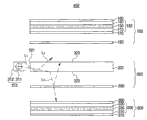
Fig. 1 is a sectional drawing, shows the liquid crystal display device according to an example embodiment of the present invention, and Fig. 2 is the sectional drawing of first display device among Fig. 1.
With reference to figure 1, liquid crystal display device comprises: first display device 100 is used to show first image; Second display device 200 is used to show second image; With light feedway (to call backlight in the following text) 300, between first and second display device 100 and 200.
As shown in Figure 2, form first transparency electrode 112 on first insulated substrate 111, it is formed by for example conductive oxide film such as tin indium oxide (ITO), thereby constitutes first substrate 110.On the second insulated substrate 121, form second transparency electrode 122, it by conductive oxide film for example for example ITO form, thereby constitute second substrate 120.First transparency electrode 112 of first substrate 110 is provided with towards second transparency electrode 122 of second substrate 120.
First liquid crystal layer 130 is made of TN (twisted-nematic) liquid crystal composition of for example 90 ° of distortions.According to present embodiment, " the Δ nd " of first liquid crystal layer 130 is about the 0.2-0.6 micron, and it is the product of the thickness (d) of the refraction ansiotropy (Δ n) and first liquid crystal layer 130, preferably is about 0.48 micron.In the liquid crystal display device of present embodiment, can adopt the liquid crystal optics condition of traditional transmission-type liquid crystal display device and do not change, thereby the reliability that prevents liquid crystal is affected.
First Polarizer 160 places on the upper surface of first display panels 150, and second Polarizer 170 is formed on the lower surface of first display panels 150.First and second Polarizers 160 and 170 absorb predetermined polarized component and allow other polarized component see through, thereby allow incident light to see through on specific direction.First and second Polarizers 160 and 170 are linear polarizations, the setting that is perpendicular to one another of its polarization axle.
Semi-transparent semi-reflecting film 180 places under second Polarizer 170, and it comprises at least two hyaline layers with the refractive index value of differing from one another, and promptly the ground floor 181 and the second layer 182 alternately pile up, as shown in Figure 3.Semi-transparent semi-reflecting film 180 partial reflections and part are transmitted into the incident light that is mapped on it.Correspondingly, the liquid crystal display device according to present embodiment has reflected light path (R) and transmitted light path (T).In reflected light path (R), incident light incides on second substrate 120, sees through first substrate 110, by semi-transparent semi-reflecting film 180 reflections, and passes second substrate 120 and penetrates.At transmitted light path (T), incident light incides on first substrate 110 from backlight 300, sees through semi-transparent semi-reflecting film 180, and passes second substrate 120 and penetrate.
Referring to Fig. 1, second display device 200 comprises second display panels 250, the 3rd Polarizer 260, the 4th Polarizer 270 once more.Second display panels 250 comprises tetrabasal 220 and second liquid crystal layer 230 between the 3rd substrate 210 and tetrabasal 220 that the 3rd substrate 210, its lower surface are provided with in the face of the 3rd substrate 210.
The 3rd Polarizer 260 places on the upper surface of second display panels 250, and the 4th Polarizer 270 is formed on the lower surface of second display panels 250.Third and fourth Polarizer 260 and 270 absorbs predetermined polarized component and allows other polarized component pass through, thereby allows incident light to pass through on specific direction.Third and fourth Polarizer 260 and 270 is linear polarizations, the setting that is perpendicular to one another of its polarization axle.
Backlight 300 is installed between first and second display device 100,200.Backlight 300 produces light, and the light that will partly be produced offers first and second display device 100,200.
As shown in Figure 1, backlight 300 comprises that photoconduction draws parts 320 and luminance control unit 330.Photoconduction draws parts 320 and is used to guide the light that produces from lamp device 310, and luminance control unit 330 controls offer the brightness of the light of first and second display device 100,200.
Photoconduction draws the shape that parts 320 have the rectangular parallelepiped plate, comprises four sides, contains the plane of incidence 321, light reflection and transmission face 322 and light-emitting face 323.Light-emitting face 323 is facing to light reflection and transmission face 322.
The first light L1 that is produced by lamp 311 passes light entrance face 321 and incides photoconduction and draw in the parts 320.Photoconduction draw parts 320 the first light L1 along separate routes to penetrate the second and the 3rd light L2, L3.Photoconduction draws parts 320 and penetrates the second light L2 or a part of first light L1 to first display device 100, penetrates the 3rd light L3 or the other parts first light L1 to second display device 200.Particularly, the second light L2 comprises from the light-emitting face 323 direct light that penetrate with by the light of light reflection and transmission face 322 reflections.The 3rd light L3 passes the light of light reflection and transmission face 322 to advance towards second display device 200.
Photoconduction draws parts 320 and light all is provided can for first and second display device 100,200.But, be difficult to allow photoconduction draw the luminance brightness that parts 320 controls offer first and second display device 100,200.So backlight 300 also comprises a luminance control unit 330 so that regulate first display device 100 and the brightness of 200 of second display device.
The material of luminance control unit 330 is not limited to the polyethylene terephthalate (PET) handled by gas-development agent.Luminance control unit 330 can be made by any material of energy partial reflection and part transmitted light.
Fig. 3 is the structural representation of semi-transparent semi-reflecting film among Fig. 1.
With reference to figure 3, when the semi-transparent semi-reflecting film 180 of hypothesis have on the z direction thickness and during along the membrane plane on x-y plane, feature according to the semi-transparent semi-reflecting film 180 of one aspect of the invention is to make that its ground floor 181 is to have refraction ansiotropy in the x-y plane at its membrane plane, and the second layer 182 does not have refraction ansiotropy in its membrane plane.Membrane plane is parallel to the plane of semi-transparent semi-reflecting film.
Semi-transparent semi-reflecting film 180 has the various transmissivities and the reflectivity Characteristics of polarization state of depending on and incident light direction.For example, the direction that is parallel to the prolonging direction (elongated direction) of semi-transparent semi-reflecting film 180 when hypothesis is the x direction, direction perpendicular to described prolonging direction is the y direction, and the second layer 182 that has the ground floor 181 of the refraction ansiotropy in high index of refraction and the membrane plane and do not have a refraction ansiotropy all has and satisfies following three principal refractive index n that concern (1)
x, n
y, n
z:
n1
x=n1
z≠n1
y;
n2
x=n2
y=n2
z;
n1
x≠n2
x;
N1
y≠ n2
yAnd
|n1
x-n2
x|<|n1
y-n2
y|--------(1)。
(n1
x, n1
y, n1
zRepresent the principal refractive index of ground floor on x axle, y axle, z axle respectively, n2
x, n2
y, n2
zRepresent the principal refractive index of the second layer on x axle, y axle, z axle respectively)
Like this, if 182 of the ground floor 181 and the second layers at the refractive index difference on the x direction less than ground floor 181 and 182 refractive index differences on the y direction of the second layer, so when a branch of nonpolarized light when the direction perpendicular to membrane plane is the incident of z direction, by Fresnel equation as can be known, the polarized component that is parallel to y direction polarization is reflected major part owing to high refractive index difference, but is parallel to the polarized component of x direction polarization because low refractive index difference will be by part transmission and reflection.
Disclosed the method that is used to strengthen display brightness, it has utilized by having the reflection-type Polarizer that birefringent dielectric multilayer film is made, and the source is that the Jap.P. spy opens communique No.9-43596 and international patent publication No.WO 97/01788.Have birefringent dielectric multilayer film and have the structure that two kinds of polymeric layers alternately pile up.A kind of polymer group that is selected from of two kinds of polymeric layers, and the another kind of polymer group that is selected from low-refraction with high index of refraction.
Hereinafter, with regard to optical characteristics, will look back the structure of dielectric multilayer film.
For example, when hypothesis wherein have high index of refraction material elongation ground floor and wherein have and have following the relation between the second layer of material elongation of low-refraction:
N1
x=n1
z=1.57, n1
y=1.86; And
n2
x=n2
y=n2
z=1.57。
So, be equal to each other and under first and second layers of situation about differing from one another first and second layers of refractive index value along the refractive index value of y direction along x direction and z direction, when nonpolarized light along perpendicular to direction (the being the z direction) incident of membrane plane the time, the polarized component of x direction is all passed through, and all is reflected according to the polarized component of Fresnel equation y direction.A representative example with birefringence dielectric multilayer film of above feature is the DBEF (Dual brightness enhancement film, two brightness enhancement films) that is made by 3M company.DBEF has sandwich construction, and wherein two kinds of films being made by different materials alternately pile up to form the hundreds of layer.In other words, PEN (polyethylene naphthalate) layer and polymethylmethacrylate (PMMA) layer with high birefringence alternately piles up to constitute the DBEF layer.Because naphthylene group has planar structure, when these groups are contiguous mutually when being provided with, be easy to pile up PEN layer and DBEF layer, make the refractive index of stacking direction become and significantly be different from the refractive index of other direction.On the contrary, arrange because PMMA is amorphous polymer and isotropy, PMMA has equal refractive index on all directions.
The polarized component of all x directions of DBEF transmission that 3M company produces, reflect the polarized component of all y directions, but according to the polarized components of semi-transparent semi-reflecting film 180 most of reflection specific directions (for example y direction) of one aspect of the invention, but partial reflection and transmission are along the polarized component perpendicular to direction (for example x direction) polarization of described specific direction.Semi-transparent semi-reflecting film 180 can form by the semi-transparent semi-reflecting films of two anisotropy of vertical connection, and the transmissivity of each film and reflectivity change with incident direction of light on polarization state and the semi-transparent semi-reflecting film 180.And, semi-transparent semi-reflecting film 180 also can be made with the isotropy reflection and the radioparent one semi-transparent semi-reflecting film that have with polarization state and incident light orientation independent by connecting the semi-transparent semi-reflecting film of an anisotropy, and the transmissivity of the semi-transparent semi-reflecting film of anisotropy and reflectivity change with polarization state and light incident direction.Two semi-transparent semi-reflecting films can be made an integrally formed structure, or make separating shaped membrane structure.
Equally, according to a further aspect in the invention, semi-transparent semi-reflecting film 180 has the isotropy transmission and reflection characteristic with polarization state and incident light orientation independent.For example, the direction of supposing to be parallel to the prolonging direction of film is the x direction, direction perpendicular to the prolonging direction of film is the y direction, ground floor 181 with high index of refraction all has the refraction isotropy with the second layer 182 with low-refraction in the x-y plane of film, first and second layer 181 and 182 all has three principal refractive index n that satisfy following relation
x, n
y, n
z:
N1
x=n1
y=n1
zAnd
n2
x=n2
y=n2
z≠n1
z------(2)
So, have under the situation of different refractivity value in the z direction at first and second layer 181 and 182, when nonpolarized light along perpendicular to direction (the being the z direction) incident of film the time, the transmission of polarized component part and the partial reflection of x direction, according to Fresnel equation, the polarized component of y direction is part transmission and partial reflection also.At this moment, can come accommodation reflex reflection of light rate, the characteristic of itself and liquid crystal display device is complementary by the thickness or the refractive index of control ground floor 181 or the second layer 182.In other words, the liquid crystal display device for reflection characteristic is strengthened improves reflectivity, and is considered to the liquid crystal display device of key factor for transmissison characteristic, improves transmissivity thereby reduce reflectivity.
As mentioned above, semi-transparent semi-reflecting film 180 among the present invention can form has anisotropic character, the transmissivity and the reflectivity that are film 180 change with polarization state and incident light direction, perhaps can form and have the isotropy feature, promptly the transmissivity of film 180 and reflectivity do not rely on polarization state and incident light direction.Which kind of situation no matter, when light along perpendicular to the direction incident of membrane plane the time, expect that semi-transparent semi-reflecting film 180 has reflectivity more than or equal to about 4% with respect to the polarized component of all directions.
Among the present invention, semi-transparent semi-reflecting film 180 can be made integrally formed structure with second Polarizer 170, perhaps makes the separating shaped chip architecture of separating with second Polarizer 170.Make under the situation of integrally formed structure with second Polarizer 170 at semi-transparent semi-reflecting film 180, can reduce the thickness of liquid crystal (LC) box, liquid crystal display device has the advantage of manufacturing cost aspect.
More than, explained the method for making semi-transparent semi-reflecting film 180 by deposition or coated polymer multilayer film to the surface of second Polarizer 170, this can contrast with the method for carrying out anti-reflex treated on Polarizer.Just, in anti-reflex treated, two kinds of hyaline membranes with different refractivity make to produce destructive interference by the multipath reflection in the polymer multi-layer film with certain thickness repeated deposition or coating.Yet, can the part transmission and the semi-transparent semi-reflecting film of partial reflection incident light in order to form, the thickness of film should be adjusted to produce constructive interference.
Fig. 4 A and 4B are sectional drawings, and the position that can be used for the light scattering layer of liquid crystal display device among Fig. 1 has been described.
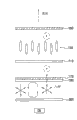
Shown in Fig. 4 A and 4B, liquid crystal display device according to present embodiment can further comprise a light scattering layer 175, it is formed on first substrate 110 or second substrate 120, so that prevent direct reflection and with suitably diffusion of various angles (diffuse) reflected light.
For example, shown in Fig. 4 A and 4B, between first substrate 110 and second Polarizer 170, or between second substrate 120 and first Polarizer 160, can form light scattering layer 175.Also can between second Polarizer 170 and semi-transparent semi-reflecting film 180, form light scattering layer 175.Light scattering layer 175 can be made integrally formed structure with second Polarizer 170 or first Polarizer 160, perhaps makes the isolating plate-like structure of separating with Polarizer 160,170.And light scattering layer 175 can be made the shape that Transparent bead is scattered in plastic foil wherein.And light scattering layer 175 can be made the state that pearl adds bonding agent, and this makes and can directly mount first substrate 110 on second Polarizer 170.
And, in order to optimize the optical efficiency of the liquid crystal display device of present embodiment, can on first substrate 110 or second substrate 120, form a phase difference plate (not drawing) according to the present invention.For example, the diffusion barrier structure that phase difference plate forms integrally formed structure or separates with Polarizer 160,170 with formation with Polarizer 160,170, described phase difference plate is between first substrate 110 and second Polarizer 170 or between second substrate 120 and first Polarizer 160.
Hereinafter, the operation mechanism that detailed description is had the liquid crystal display device of above structure.
Fig. 5 A is the synoptic diagram of the operation mechanism of explanation liquid crystal display device transmission mode and reflective-mode to Fig. 6 B, and the wherein semi-transparent semi-reflecting film 180 and second Polarizer 170 are made integrally formed structure together.Here, the expression of light polarization direction is based on the polarization axle of first Polarizer 160, and partial reflection light and part transmitted light are expressed as dotted line.
At first, under reflective-mode, when not applying pixel voltage (OFF), shown in Fig. 5 A,, make the direction linear polarization of light along the polarization axle that is parallel to first Polarizer 160 from light transmission first Polarizer 160 of external source incident.The liquid crystal layer 130 and first transparency electrode 112 are passed in the linear polarization transmittance, make linearly polarized photon along direction linear polarization, then incide the semi-transparent semi-reflecting film 180 of making integrally formed structure with second Polarizer 170 perpendicular to the polarization axle of first Polarizer 160.At this moment, because the polarization axle of second Polarizer 170 is perpendicular to the polarization axle of first Polarizer 160, the light that incides second Polarizer 170 becomes the direction with the polarization axle that is parallel to second Polarizer 170.Therefore, partly see through semi-transparent semi-reflecting film 180 and partly by semi-transparent semi-reflecting film 180 reflections along the light of the direction linear polarization that is parallel to second Polarizer, 170 polarization axles.That is to say, have at semi-transparent semi-reflecting film 180 under the situation of refractive properties of relation (1), incide light in the semi-transparent semi-reflecting film 180 along the partly transmission and the partly reflection of polarized component of the x direction polarization of the prolonging direction that is parallel to semi-transparent semi-reflecting film 180, and the edge is reflected perpendicular to the polarized component major part of the direction polarization of described prolonging direction.And, have at semi-transparent semi-reflecting film 180 under the situation of refractive properties of relation (2), for the light that incides in the semi-transparent semi-reflecting film 180, along the transmission of polarized component part and the partial reflection of x direction and y direction polarization.
So, by linear polarization light transmission first transparency electrode 112 and the liquid crystal layer 130 of 180 reflections of semi-transparent semi-reflecting film, make its direction linear polarization along the polarization axle that is parallel to first Polarizer 160.Afterwards, light transmission first Polarizer 160, thereby display white image.And the light that sees through semi-transparent semi-reflecting film 180 is stored between semi-transparent semi-reflecting film 180 and the backlight 300, and the light of storage repeatedly carries out the process of part transmissive portions sub reflector.As a result, light loss is eliminated, and reflectivity and optical efficiency are enhanced.
Under reflective-mode, when applying maximum pixel voltage (ON), shown in Fig. 5 B,, make the direction linear polarization of light along the polarization axle that is parallel to first Polarizer 160 from light transmission first Polarizer 160 of external source incident.Afterwards, linear polarization light transmission liquid crystal layer 130, polarization state does not change, then incide with the integrally formed semi-transparent semi-reflecting film 180 of second Polarizer 170 in.At this moment, owing to the polarization axle of linearly polarized photon perpendicular to second Polarizer 170, light is all absorbed by second Polarizer 170.So, linearly polarized photon can not reflected by semi-transparent semi-reflecting film 180, thereby shows picture black.
Under transmission mode, when not applying pixel voltage (OFF), as shown in Figure 6A, from the light of backlight 300 radiation incide with the integrally formed semi-transparent semi-reflecting film 180 of second Polarizer 170.Have at semi-transparent semi-reflecting film 180 under the situation of refracting characteristic of relation (1), the polarized component of the polarization axle that is parallel to second Polarizer 170 of light (it is parallel to x direction polarization) is by partly transmission and reflection, and the polarized component major part that is parallel to y direction polarization is reflected.And, have at semi-transparent semi-reflecting film 180 under the situation of refracting characteristic of relation (2), be parallel to the transmission of light part and the partial reflection of the polarization axle of second Polarizer 170, because along all transmission of polarized component part and reflections of x direction and y direction polarization.
The light that so, has seen through the semi-transparent semi-reflecting film 180 and second Polarizer 170 becomes the linearly polarized photon that orientation of oscillation is parallel to the polarization axle of second Polarizer 170.Linear polarization light transmission first transparency electrode 112 and liquid crystal 130 make it along the direction linear polarization that is parallel to the polarization axle of first Polarizer 160.Therefore, along described light transmission first Polarizer 160 of direction linear polarization of the polarization axle that is parallel to first Polarizer 160, thus the display white image.Equally, be stored between backlight 300 and the semi-transparent semi-reflecting film 180 by the light of semi-transparent semi-reflecting film 180 reflections, and carry out above step repeatedly then.Like this, be parallel to the polarized component of x direction or be parallel to the x direction and the polarized component adjoining land of y direction sees through semi-transparent semi-reflecting film 180 to be utilized, make light loss reduce, transmissivity and optical efficiency improve.
Under transmission mode, when applying maximum pixel voltage (ON), shown in Fig. 6 B, from the light of backlight 300 radiation incide with the integrally formed semi-transparent semi-reflecting film 180 of second Polarizer 170, make the transmission of light portion ground and the reflection of the polarization axle that is parallel to second Polarizer 170.The light that has seen through the semi-transparent semi-reflecting film 180 and second Polarizer 170 is converted into the light of direction along the polarization axle that is parallel to second Polarizer 170 (that is, along the direction perpendicular to the polarization axle of first Polarizer 160) linear polarization.This linear polarization light transmission first transparency electrode 112 and liquid crystal layer 130, polarization state does not change.Therefore, the edge can not see through first Polarizer 160 perpendicular to the light of the direction linear polarization of first Polarizer, 160 polarization axles, thereby shows picture black.
Fig. 7 A is the synoptic diagram of explanation liquid crystal display device operation mechanism under transmission mode and reflective-mode to Fig. 8 B, and wherein semi-transparent semi-reflecting film 180 separates with second Polarizer 170, and forms schistose texture.Here, the expression of light polarization direction is based on the polarization axle of first Polarizer 160, and partial reflection light and part transmitted light be illustrated by the broken lines.
At first, under reflective-mode, when not applying pixel voltage (OFF), shown in Fig. 7 A,, make the direction linear polarization of light along the polarization axle that is parallel to first Polarizer 160 from light transmission first Polarizer 160 of external source incident.This linear polarization light transmission liquid crystal layer 130 and first transparency electrode 112 make linearly polarized photon along the direction linear polarization perpendicular to the polarization axle of first Polarizer 160, then incide in second Polarizer 170.At this moment, because the polarization axle of second Polarizer 170 is perpendicular to the polarization axle of first Polarizer 160, just sees through second Polarizer 170 and then incide in the semi-transparent semi-reflecting film 180 along light perpendicular to the direction linear polarization of the polarization axle of first Polarizer 160.Have at semi-transparent semi-reflecting film 180 under the situation of refracting characteristic of relation (1), incide light in the semi-transparent semi-reflecting film 180 along the polarized component of x direction polarization of the prolonging direction that is parallel to semi-transparent semi-reflecting film 180 by part transmission and reflection, and be reflected along polarized component major part perpendicular to the y direction polarization of prolonging direction.And, have at semi-transparent semi-reflecting film 180 under the situation of refracting characteristic of relation (2), for the light that incides in the semi-transparent semi-reflecting film 180, along the polarized component of x direction and y direction polarization by part transmission and partial reflection.
So, owing to the polarization axle that is parallel to second Polarizer 170 by the linearly polarized photon of semi-transparent semi-reflecting film 180 reflections, it sees through second Polarizer 170, and incides in the liquid crystal layer 130 via first transparency electrode 112.Linear polarization light transmission liquid crystal layer 130, thus it is along the direction linear polarization of the polarization axle that is parallel to first Polarizer 160.Afterwards, light transmission first Polarizer 160, thereby display white image.And the light that has seen through semi-transparent semi-reflecting film 180 is stored between semi-transparent semi-reflecting film 180 and the backlight 300, and the light of storage repeats the process of part transmissive portions sub reflector.As a result, optical loss reduces, and reflectivity and optical efficiency improve.
Under reflective-mode, when applying maximum pixel voltage (ON), shown in Fig. 7 B,, make the direction linear polarization of light along the polarization axle that is parallel to first Polarizer 160 from light transmission first Polarizer 160 of external source incident.Afterwards, this linear polarization light transmission liquid crystal layer 130, polarization state is constant, incides then in second Polarizer 170.At this moment, owing to the polarization axle of linearly polarized photon perpendicular to second Polarizer 170, light will all be absorbed by second Polarizer 170.So, because linearly polarized photon can will not shown black image by semi-transparent semi-reflecting film 180 reflections.
Under transmission mode, when not applying pixel voltage (OFF), shown in Fig. 8 A, incide the semi-transparent semi-reflecting film 180 from the light of backlight 300 radiation, make transmission of light part and reflection.Have at semi-transparent semi-reflecting film 180 under the situation of refracting characteristic of relation (1), incided light in the semi-transparent semi-reflecting film 180 along the polarized component of x direction polarization of the prolonging direction that is parallel to semi-transparent semi-reflecting film 180 by part transmission and reflection, and be reflected along polarized component major part perpendicular to the y direction polarization of prolonging direction.And, have at semi-transparent semi-reflecting film 180 under the situation of refracting characteristic of relation (2), incide light in the semi-transparent semi-reflecting film 180 along the polarized component of x direction and y direction polarization by part transmission and reflection.
So, seen through the direction linear polarization of the light of the semi-transparent semi-reflecting film 180 and second Polarizer 170 along the polarization axle that is parallel to second Polarizer 170.Afterwards, linear polarization light transmission first transparency electrode 112 and liquid crystal 130 make its direction linear polarization along the polarization axle that is parallel to first Polarizer 160.Therefore, along light transmission first Polarizer 160 of the direction linear polarization of the polarization axle that is parallel to first Polarizer 160, thus the display white image.And, be stored between backlight 300 and the semi-transparent semi-reflecting film 180 by the light of semi-transparent semi-reflecting film 180 reflections, carry out above step then repeatedly.Like this, be parallel to the polarized component of x direction polarization or be parallel to the x direction and the polarized component adjoining land of y direction polarization sees through semi-transparent semi-reflecting film 180 and is utilized, thereby light loss reduces, transmissivity and optical efficiency improve.
Under transmission mode, when applying maximum pixel voltage (ON), shown in Fig. 8 B, incide the semi-transparent semi-reflecting film 180 from the light of backlight 300 radiation, make the semi-transparent semi-reflecting film 180 of incident light part transmission and by semi-transparent semi-reflecting film 180 partial reflections.Second Polarizer 170 is passed in the transmittance that has seen through semi-transparent semi-reflecting film 180, makes it convert the light of the polarization axle that is parallel to second Polarizer 170 direction of the polarization axle of first Polarizer 160 (promptly perpendicular to) linear polarization to.Afterwards, this linear polarization light transmission first transparency electrode 112 and liquid crystal layer 130 and polarization state does not change.Therefore, the edge can not see through first Polarizer 160 perpendicular to the light of the direction linear polarization of the polarization axle of first Polarizer 160, thereby shows picture black.
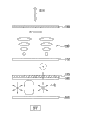
Fig. 9 is the structural representation of liquid crystal display device, also comprises light reflection graphic patterns and optical sheet, and Figure 10 is a plan view, has shown to draw the light reflection graphic patterns that forms on the parts at photoconduction among Fig. 9.
Referring to Fig. 9, light reflection graphic patterns 322a is formed on the reflection and transmission face 322 that photoconduction draws parts 320, so that towards luminance control unit 330.Light reflection graphic patterns 322a partly is reflected into the light that is mapped on the light reflection and transmission face 322, and changes the light path that incides the light on the light reflection and transmission face 322, makes a part that incides the light on the light reflection and transmission face 322 to advance towards light-emitting face 323.
Light reflection graphic patterns 322a is formed on the light reflection and transmission face 322.For example, light reflection graphic patterns 322a is included in a plurality of points that are arranged in matrix shape on the light reflection and transmission face 322.By silk screen print method, the slurry of the material that is mixed with the high light reflectivity rate is printed on the light reflection and transmission face 322, make light reflection graphic patterns 322a be formed on the light reflection and transmission face 322.
The light reflection graphic patterns 322a that is formed on the light reflection and transmission face 322 can be the various patterns with specific regularity.For example, the point of light reflection graphic patterns 322a is arranged in matrix shape on light reflection and transmission face 322, the proportional increase of distance that the size of each point and each point and light entrance face are 321.In other words, the point of light reflection graphic patterns 322a has different size, makes the closer to the size of the point of light entrance face 321 more little.The size of the point of light reflection graphic patterns 322a is decided by a little and the distance of 321 of light entrance faces, makes that the light reflectivity by light reflection graphic patterns 322a keeps basically identical on the whole surface of light reflection and transmission face 322.
Again with reference to figure 9, to draw in the parts 320 at the photoconduction of present embodiment, the vertical range that light reflection and transmission face 322 and light-emitting face are 323 is a basically identical.In other words, light reflection and transmission face 322 is arranged essentially parallel to light-emitting face 323.
Yet in another embodiment, light reflection and transmission face 322 can be not parallel to light-emitting face 323.Especially, proportional the reducing of distance of 321 of point on vertical range between light reflection and transmission face 322 and the light-emitting face 323 and the light-emitting face (or light reflection and transmission face 322) and light entrance faces.Preferably, the vertical range of 323 of light reflection and transmission face 322 and light-emitting faces little by little reduces.For example, light-emitting face 323 is parallel to display panels, the angle that light reflection and transmission face 322 tilts to be scheduled to respect to light-emitting face 323.
On the other hand, as shown in Figure 9, first optical sheet 340 is installed on the light-emitting face 323 that photoconduction draws parts 320, so that strengthen the optical characteristics of drawing the light that parts 320 penetrate from photoconduction by changing the optical profile of drawing the light that parts 320 penetrate from photoconduction.First optical sheet 340 also comprises first diffusion disk 342 and first prismatic lens 344.Especially, first diffusion disk 342 scatterings, the second light L2 and part the 3rd light L3 that is reflected by luminance control unit 330, thus uniform Luminance Distribution is provided.According to an example embodiment of the present invention, at least one first prismatic lens 344 is installed on first diffusion disk 342, thereby increases from the visual angle of the light of first diffusion disk, 342 ejaculations by proofreading and correct the direction of light that penetrates from first diffusion disk 342.
In addition, second optical sheet 350 can be installed between the luminance control unit 330 and second display panels 200, so that the optical characteristics of other parts the 3rd light L3 that strengthen to see through luminance control unit 330 and advance towards second display panels then, this is to realize by the optical profile that changes described other parts the 3rd light L3.Second optical sheet 350 also can comprise one second diffusion disk 352 and one second prismatic lens 354.Especially, described other parts the 3rd light L3 of second diffusion disk, 352 scatterings, thus a uniform Luminance Distribution is provided.Second prismatic lens 354 is proofreaied and correct the direction of light that penetrates from second diffusion disk 352, thereby increases from the visual angle of the light of second diffusion disk, 352 ejaculations.
Though first display device 100 has identical size with second display device 200 in the embodiment of Fig. 1 to 9, first display device 100 and second display device 200 can be of different sizes.
Figure 11 is a sectional drawing, has shown according to the present invention the liquid crystal display device of another example embodiment.
Referring to Figure 11, liquid crystal display device 600 comprises: one first 100, one of display device has second display device 500 of the size that is different from first display device 100, and the backlight 300 between first and second display device 100,500.
First viewing area of first display device 100 is different from second viewing area of second display device 500, and in the present embodiment, first viewing area of first display device 100 is bigger than second viewing area of second display device 500.
When first viewing area of first display device 100 was bigger than second viewing area of second display device 500, the optical characteristics of second display device 500 changed along with the position of second display device 500.
As shown in figure 11, an end of second display device 500 and photoconduction draw light entrance face 321 alignment of parts 320.When light entrance face 321 alignment that an end and the photoconduction of second display device 500 draws parts 320, when being positioned at other position, a end when second display device 500 compares, and can be at the light of second display device, 500 places collection greater number.
Though do not show in Figure 11, an end of second display device 500 can leave light entrance face 321 1 preset distances and install.For example, second display device 500 places photoconduction to draw the core of the light reflection and transmission face 322 of parts 320.In this case, shortcoming is the restriction that exists for brightness, but advantage is the restriction of installing is reduced.In addition, the other end of second display device 500 relative with an end of second display device 500 can draw side parts 320, relative with light entrance face 321 with photoconduction and aligns.
Figure 12 is a sectional drawing, has shown according to the present invention the liquid crystal display device of another example embodiment, and Figure 13 shows first display device among Figure 12.
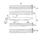
Referring to Figure 12, liquid crystal display device 900 comprises: first display device 700 is used to show first image; Second display device 200 is used to show second image; With backlight 800, place between first and second display device 700,200.First display device 700 comprises first display panels 750, first Polarizer 760, second Polarizer 770 and semi-transparent semi-reflecting film 780.
Referring to Figure 13, first display panels 750 comprises first substrate 710, faces second substrate 720, the liquid crystal layer 730 between first substrate 710 and second substrate 720 that first substrate 710 is provided with.
Particularly, first substrate 710 comprises first insulated substrate 711.On first insulated substrate 711, form a plurality of on-off elements or thin film transistor (TFT) (TFT) 712 and first transparency electrode (or pixel electrode) 714 that is electrically connected to TFT 712.TFT 712 is arranged in matrix structure on first insulated substrate 711.The gate electrode 712a of TFT712 is connected to the gate line (not drawing) that extends at first insulated substrate, 711 upper edge line directions, and the source electrode 712b of TFT 712 is connected to the data line (not drawing) that extends at first insulated substrate, 711 upper edge column directions.The drain electrode 712c of TFT 712 is electrically connected to by first transparency electrode of making such as the conductive oxide film of tin indium oxide (ITO) 714.
An organic insulator 713 is formed between the TFT 712 and first transparency electrode 714.Organic insulator 713 comprises the contact hole 713a that exposes drain electrode 712c.Organic insulator 713 makes TFT 712 and 714 insulation of first transparency electrode, allows first transparency electrode 714 only contact drain electrode 712c simultaneously.
Referring again to Figure 12, second display device 200 comprises second display panels 250, the 3rd Polarizer 260 and the 4th Polarizer 270.The tetrabasal 220 that second display panels comprises the 3rd substrate 210, be provided with facing to the 3rd substrate 210 and be placed on second liquid crystal layer 230 between the 3rd substrate 210 and the tetrabasal 220.The 3rd Polarizer 260 is placed on the upper surface of second display panels 250, and the 4th Polarizer 270 is placed on the lower surface of second display panels 250.
Though in Figure 12, do not draw, second display panels 250 can with the same enforcement of first display panels 750 among Figure 13.
First photoconduction draws parts 820 and comprises four sides, contains first light entrance face, 821, the first smooth reflection and transmission face 822 and first light-emitting face 823.First light-emitting face 823 is facing to the first smooth reflection and transmission face 822.
Pass first light entrance face 821 incide first photoconduction draw the first light L1 in the parts 820 by following path by along separate routes, to advance towards first and second display device 700,200.First photoconduction draw parts 820 with the first light L1 along separate routes to penetrate the third and fourth light L3, L4.First photoconduction draws parts 820 and penetrates the 3rd light L3 or the part first light L1 to first display device 700, and penetrates the 4th light L4 or the other parts first light L1 to second display device 200.Particularly, the 3rd light L3 comprises direct the reflection from the light of first light-emitting face, 823 ejaculations with by the first smooth reflection and transmission face 822 and passes the light that first light-emitting face 823 penetrates.The 4th light L4 passes the first smooth reflection and transmission face 822 and advances to second display device 200.
Second photoconduction draws parts 830 and is arranged between first and second display device 700,200, more specifically be arranged at the first reflection and transmission face 822 near.Second photoconduction draws parts 830 and comprises four sides, contains the second light L2 and incides second light entrance face 831 on it, the second smooth reflection and transmission face 832 and one second light-emitting face 833.Second light-emitting face 833 is in the face of the second smooth reflection and transmission face 832.
Pass second light entrance face 831 incide second photoconduction draw the second light L2 in the parts 830 by following path by along separate routes, to advance to first and second display device 700,200.Second photoconduction draws parts 830 with the second light L2 along separate routes, to penetrate the 5th and the 6th light L5, L6.Second photoconduction draws parts 830 and penetrates the 6th light L6 or the part second light L2 to first display device 700, and penetrates the 5th light L5 or the other parts second light L2 to second display device 200.Particularly, the 5th light L5 comprises direct the reflection from the light of second light-emitting face, 833 ejaculations with by the second smooth reflection and transmission face 832 and passes the light that second light-emitting face 833 penetrates.The 6th light L6 passes the second smooth reflection and transmission face 832 and advances to first display device 700.
Pass first photoconduction draw parts 820 the first smooth reflection and transmission face 822 the 4th light L4 and pass the 6th light L6 that second photoconduction draws the second smooth reflection and transmission face 832 of parts 830 and arrive luminance control unit 840.Luminance control unit 840 antireflection parts the 4th light L4, offer first display device 700 so that parts 820 are drawn via first photoconduction in the described reflecting part of the 4th light L4, and transmission other parts the 4th light L4 is to offer second display device 200 with described other parts the 4th light L4.In addition, luminance control unit 840 antireflection parts the 6th light L6, offer second display device 200 so that parts 830 are drawn via second photoconduction in the described reflecting part of the 6th light L6, and transmission other parts the 6th light L6 is to offer first display device 700 with described other parts the 6th light L6.
Second brightness at first brightness at first display device, 700 places and second display device, 200 places is accurately controlled by the light reflectivity and the light transmission of control luminance control unit 840.Like this, the ratio of first brightness and second brightness can accurately be controlled by the light reflectivity and the light transmission of control luminance control unit 840.
In this embodiment, it is flat type photoconduction corbel back slabs that first photoconduction draws parts 820, and wherein the vertical range of 823 of the first smooth reflection and transmission face 822 and first light-emitting faces is even substantially.It also is flat type photoconduction corbel back slab that second photoconduction draws parts 830.Yet first and second photoconductions draw parts can be wedge shape, and wherein the vertical range between light reflection and transmission face and light-emitting face gradually changes.
Figure 14 is the structural representation of the liquid crystal display device of Figure 12, also comprises light reflection graphic patterns and optical sheet.
Referring to Figure 14, the first smooth reflection graphic patterns 822a is formed at first photoconduction and draws on the first reflection and transmission face 822 of parts 820, and the second smooth reflection graphic patterns 832a is formed at second photoconduction and draws on the second reflection and transmission face 832 of parts 830.For example, the first and second smooth reflection graphic patterns 822a, 832a comprise a plurality of points that are arranged in matrix shape.
Proportional the increasing continuously of distance that the point of the size of the each point of the first smooth reflection graphic patterns 822a and the first smooth reflection graphic patterns 822a and first light entrance face are 821.Proportional the increasing continuously of distance that the point of the size of the each point of the second smooth reflection graphic patterns 832a and the second smooth reflection graphic patterns 832a and second light entrance face are 831.
On the other hand, as shown in figure 14, backlight 800 also comprises first optical sheet 850 and second optical sheet 860.Particularly, first optical sheet 850 is installed between first display device 700 and first light-emitting face 823, and second optical sheet 860 is installed between second display device 200 and second light-emitting face 833.
First optical sheet 850 has increased the visual angle of part the 3rd light L3 and part the 4th light L4, and described part the 3rd light L3 of diffusion and described part the 4th light L4 are to provide uniform Luminance Distribution.Second optical sheet 860 has increased the visual angle of part the 5th light L5 and part the 6th light L6, and described part the 5th light L5 of diffusion and described part the 6th light L6 are so that provide uniform Luminance Distribution.
Figure 15 is the sectional drawing of the liquid crystal display device of another example embodiment according to the present invention.
Referring to Figure 15, liquid crystal display device 1200 comprises: first display device 700 has second display device 1000 of the size that is different from first display device 700, and places the backlight 1100 between first and second display device 700,1000.
In this embodiment, first viewing area of first display device 700 is bigger than second viewing area of second display device 1000, and first and second photoconductions draw parts 1120,1130 to has respectively and the first and second viewing area matched size separately.The surface region that first photoconduction draws parts 1120 draws the surface region of parts 1130 greater than second photoconduction.Yet in another embodiment, first viewing area of first display device can be littler than second viewing area of second display device.
As shown in figure 15, the first smooth reflection graphic patterns 1122a is formed at first photoconduction and draws on the first reflection and transmission face 1122 of parts 1120, and the second smooth reflection graphic patterns 1132a is formed at second photoconduction and draws on the second reflection and transmission face 1132 of parts 1130.In this embodiment, the first and second smooth reflection graphic patterns 1122a, 1132a comprise a plurality of points that are arranged in matrix shape separately.Because the surface region that first photoconduction draws parts 1120 draws the surface region of parts 1130 greater than second photoconduction, the structure that is formed on the first smooth reflection graphic patterns 1122a on the first reflection and transmission face 1122 is different from the structure that is formed on the second smooth reflection graphic patterns 1132a on the second reflection and transmission face 1132.
For example, distance among first (or second) the light reflection graphic patterns 1122a (1132a) between point and first (or second) light entrance face 1121 (1131) of size and first (or second) the light reflection graphic patterns 1122a (1132a) of each point increases continuously pro rata, but the size of each point is different from the size of each point among the second smooth reflection graphic patterns 1132a among the first smooth reflection graphic patterns 1122a.In other words, with regard to the size of the point of the second reflection graphic patterns 1132a, the ratio of its change in size and device variable in distance will be higher than the ratio of change in size and device variable in distance of the point of the first reflection graphic patterns 1132a.
Though not shown among Figure 15, backlight 1100 also can comprise first optical sheet and second optical sheet.First optical sheet can be installed between first display device 700 and first light-emitting face 1123, and second optical sheet can be installed between second display device 1000 and second light-emitting face 1133.Preferably, the surface region of first and second optical sheets draws the surface region coupling of parts 1120,1130 dimensionally respectively with first and second photoconductions.
Figure 16 is the sectional drawing of the liquid crystal display device of another example embodiment according to the present invention.
Referring to Figure 16, liquid crystal display device comprises: first display device, 700, the second display device 1300, and place backlight 800 between first and second display device 700,1300.
The first semi-transparent semi-reflecting film 780 places below second Polarizer 770 or 800 of second Polarizer 770 and backlights, and it comprises at least two hyaline layers that refractive index value differs from one another, that is, the ground floor and the second layer alternately pile up with form more than or equal two-layer.First semi-transparent semi-reflecting film 780 partial reflections and part are transmitted into the light that is mapped on it.Therefore, first display device 700 is utilized reflected light and transmitted light display image.
The second semi-transparent semi-reflecting film 1380 places between the 3rd Polarizer 1360 and the backlight 800, and it comprises at least two hyaline layers that refractive index value differs from one another, that is, the ground floor and the second layer alternately pile up with form more than or equal two-layer.Second semi-transparent semi-reflecting film 1380 partial reflections and part are transmitted into the light that is mapped on it.Therefore, second display device 1300 utilizes reflected light and transmitted light to come display image.
Although below detailed invention has been described, should be appreciated that under the situation that does not depart from the spirit of the present invention that is defined by the following claims and category, can carry out various variations, substitute and change the present invention.
Claims (32)
1. liquid crystal display device comprises:
First display device comprises:
First display panels has first substrate, is arranged on second substrate, and first liquid crystal layer between this first and second substrate of described first substrate top,
Place the semi-transparent semi-reflecting film below this first display panels, this semi-transparent semi-reflecting film has the multilayer that ground floor that wherein refractive index is different separately and the second layer alternately pile up, the incident light that makes this semi-transparent semi-reflecting membrane portions reflection and part be transmitted into to be mapped on this semi-transparent semi-reflecting film and
Place first Polarizer on this first display panels and place this first display panels and this semi-transparent semi-reflecting film between second Polarizer;
Second display device that comprises second display panels, this second display panels have the 3rd substrate, tetrabasal and second liquid crystal layer between this third and fourth substrate; And
Place the light feedway between this first and second display device, this light feedway comprises:
Light source produces first light,
The photoconduction that is used to receive described first light draws parts, with the first of this first light as second light offer this first display device and with the second portion of this first light as the 3rd light offer this second display device and
Luminance control unit, the quantity of this first and second part that controls this first light is to adjust the contrast ratio of brightness between this first and second display device.
2. liquid crystal display device as claimed in claim 1, wherein this semi-transparent semi-reflecting film and this second Polarizer are integrally formed.
3. liquid crystal display device as claimed in claim 1, wherein this semi-transparent semi-reflecting film separates formation to have sheet with this second Polarizer.
4. liquid crystal display device as claimed in claim 1, wherein this semi-transparent semi-reflecting film has transmissivity and reflectivity along with polarization state and described incident direction of light and the anisotropic properties that changes.
5. liquid crystal display device as claimed in claim 4, wherein when this semi-transparent semi-reflecting film have along the thickness of z direction and be parallel to the surface of this semi-transparent semi-reflecting film, during along the membrane plane on x-y plane, this ground floor and this second layer have three principal refractive index n that satisfy following relation respectively
x, n
yAnd n
z:
n1
x=n1
z≠n1
y;
n2
x=n2
y=n2
z;
n1
x≠n2
x;
N1
y≠ n2
yAnd
|n1
x-n2
x|<|n1
y-n2
y|,
N1 wherein
x, n1
yAnd n1
zRepresent this ground floor respectively in the principal refractive index of x direction, y direction and z direction, n2
x, n2
yAnd n2
zRepresent that this second layer is respectively in the principal refractive index of x direction, y direction and z direction.
6. liquid crystal display device as claimed in claim 1, wherein this semi-transparent semi-reflecting film has isotropy transmission and the reflection characteristic with the orientation independent of polarization state and this incident light.
7. liquid crystal display device as claimed in claim 6, wherein when this semi-transparent semi-reflecting film have along the thickness of z direction and be parallel to the surface of this semi-transparent semi-reflecting film, during along the membrane plane on x-y plane, this ground floor and this second layer have three principal refractive index n that satisfy following relation respectively
x, n
yAnd n
z:
N1
x=n1
y=n1
zAnd
n2
x=n2
y=n2
z≠n1
z,
N1 wherein
x, n1
yAnd n1
zCharacterize this ground floor respectively in the principal refractive index of x direction, y direction and z direction, n2
x, n2
yAnd n2
zCharacterize this second layer respectively in the principal refractive index of x direction, y direction and z direction.
8. liquid crystal display device as claimed in claim 1, wherein cremasteric reflex path and transmission path in this first display device, the light of advancing via this reflection paths incides on the front surface of this first display panels and by this semi-transparent semi-reflecting film and reflexes to this first display panels, penetrate with this front surface via this first display panels, and inciding on the rear surface of this first display panels from this light feedway behind semi-transparent semi-reflecting film by this via the light that this transmission path is advanced, to penetrate via this first display panels.
9. liquid crystal display device as claimed in claim 1, wherein this semi-transparent semi-reflecting film is made up of the first semi-transparent semi-reflecting layer and the second semi-transparent semi-reflecting layer, transmissivity of this first semi-transparent semi-reflecting layer and reflectivity change with polarization state and this incident direction of light, and this second semi-transparent semi-reflecting layer has isotropy transmission and the reflection characteristic with this orientation independent of this polarization state and this incident light.
10. liquid crystal display device as claimed in claim 1, wherein this first display device also comprises light scattering layer.
11. liquid crystal display device as claimed in claim 1, wherein this semi-transparent semi-reflecting film is formed by all having the transmissivity that changes along with polarization state and this incident direction of light and the semi-transparent semi-reflecting layer of two anisotropy of reflectivity.
12. as the liquid crystal display device of claim 10, wherein this light scattering layer is between this first substrate and this second Polarizer.
13. as the liquid crystal display device of claim 10, wherein this light scattering layer is between this second substrate and this first Polarizer.
14. as the liquid crystal display device of claim 10, wherein this light scattering layer is between this second Polarizer and this semi-transparent semi-reflecting film.
15. liquid crystal display device as claimed in claim 1, wherein this second display device also comprises:
The 3rd Polarizer places on the first surface of this second display panels; And
The 4th Polarizer places on the second surface of this second display panels.
16. liquid crystal display device as claimed in claim 1, wherein this photoconduction draws parts and comprises:
Light entrance face is used to receive this first light;
Light reflection and transmission face is used to reflect this second light and arrives this second display device to this first display device and transmission the 3rd light; And
Light-emitting face, relative with this light reflection and transmission face, be used to penetrate this second light.
17. liquid crystal display device as claim 16, the light reflection graphic patterns that wherein has a plurality of points is formed on this light reflection and transmission face, the size of those points is different make further from the points of this light entrance face bigger and be proportional to distance between respective point and this light entrance face than the point of more close this light entrance face.
18. liquid crystal display device as claimed in claim 1, wherein this luminance control unit in the form of sheets.
19., comprise also being used for changing the optical profile of this second light that this optical sheet places this photoconduction to draw between parts and this semi-transparent semi-reflecting film so that improve the optical sheet of the optical characteristics of this second light as the liquid crystal display device of claim 16.
20. liquid crystal display device as claimed in claim 1, wherein the brightness that records at this first display device place is higher than the brightness that records at this second display device place.
21. liquid crystal display device as claimed in claim 1, wherein the surface region of this first display panels has the size of the surface region that equals this second display panels substantially.
22. liquid crystal display device as claimed in claim 1, wherein the surface region of this first display panels is greater than the surface region of this second display panels.
23. a liquid crystal display device comprises:
First display device comprises:
First display panels has first substrate, second substrate and places first liquid crystal layer between this first and second substrate, and
Place the first following semi-transparent semi-reflecting film of this first display panels, this first semi-transparent semi-reflecting film has wherein the multilayer that refractive index is different separately ground floor and the second layer alternately pile up, and makes this first semi-transparent semi-reflecting membrane portions reflection and part be transmitted into first incident ray that is mapped on this first semi-transparent semi-reflecting film;
Second display device that comprises second display panels, this second display panels have the 3rd substrate, tetrabasal and place second liquid crystal layer between this third and fourth substrate; And
Place the light feedway between this first and second display device, this light feedway will be that first light of the first of the light that produces of light source is divided into the 3rd light and the 4th light is supplied with this third and fourth light respectively to give this first and second display device, and will be that second light of the second portion of this light of producing of this light source is divided into the 5th light and the 6th light is supplied with the 5th and the 6th light respectively to give this second and first display device, this light feedway controls the 3rd, the 4th, the quantity of the 5th and the 6th light is to regulate the brightness contrast rate between this first and second display device.
24. liquid crystal display device as claim 23, wherein at least one on-off element and the transparent pixels electrode that is electrically connected to this on-off element are formed on this first substrate, and are formed on this second substrate in the face of a transparent common electrode of this transparent pixels electrode.
25. as the liquid crystal display device of claim 24, wherein this on-off element is a thin film transistor (TFT).
26. as the liquid crystal display device of claim 23, wherein this light feedway comprises:
Light source is used to produce described light;
First photoconduction draws parts, is used to receive this first light, is used for the 3rd light is offered this first display device, and is used for transmission the 4th light to this second display device;
Second photoconduction draws parts, is used for receiving this second light, is used for the 5th light is offered this second display device, and is used for transmission the 6th light to this first display device;
Luminance control unit, place between this first and second display device, be used to reflect the first of the 4th light to this first display device, the second portion that is used for transmission the 4th light is to this second display device, the first that is used for transmission the 6th light is to this first display device, and the second portion that is used to reflect the 6th light is to this second display device, thereby controls the brightness contrast rate between this first and second display device.
27. as the liquid crystal display device of claim 26, wherein this first photoconduction draws parts and comprises:
First plane of incidence is used to receive this first light;
The first smooth reflection and transmission face is used to reflect the 3rd light to this first display device be used for transmission the 4th light to this second display device; And
First light-emitting face is positioned at the opposite of this light reflection and transmission face, is used to penetrate the 3rd light, and
This second photoconduction draws parts and comprises:
Second plane of incidence is used to receive this second light;
The second smooth reflection and transmission face is used to reflect the 5th light to this second display device, and is used for transmission the 6th light to this first display device; And
Second light-emitting face is positioned at the opposite of this second smooth reflection and transmission face, allows the 5th light penetrate.
28. liquid crystal display device as claim 27, wherein having the first a plurality of smooth reflection graphic patterns at first is formed on this first smooth reflection and transmission face, having the second a plurality of smooth reflection graphic patterns at second is formed on this second smooth reflection and transmission face, wherein said first has the different size that is proportional to the distance between and this first light entrance face at this first, make win apart from this first light entrance face far away more this first big more, this second has the different size that is proportional to the distance between and this second light entrance face at this second, make second apart from this second light entrance face far away more this second big more.
29. liquid crystal display device as claim 28, wherein this first photoconduction surface region of drawing parts draws the surface region of parts greater than this second photoconduction, and this second has than the size of the higher change in size of described first change in size and the ratio of device variable in distance with the ratio of device variable in distance.
30. as the liquid crystal display device of claim 23, wherein the size of the surface region of this first display panels equals the size of the surface region of this second display panels substantially.
31. as the liquid crystal display device of claim 23, wherein the surface region of this first display panels is greater than the surface region of this second display panels.
32. liquid crystal display device as claim 23, wherein this second display device also comprises the second semi-transparent semi-reflecting film that is positioned between this second display panels and this light feedway, this second semi-transparent semi-reflecting film has wherein the 3rd layer different separately and the 4th layer of multilayer of alternately piling up of refractive index, makes this second semi-transparent semi-reflecting membrane portions reflection and part be transmitted into second incident ray that is mapped on this second semi-transparent semi-reflecting film.
Applications Claiming Priority (2)
| Application Number | Priority Date | Filing Date | Title |
|---|---|---|---|
| KR1020020044264 | 2002-07-26 | ||
| KR1020020044264A KR100828531B1 (en) | 2002-07-26 | 2002-07-26 | Liquid crystal display |
Publications (2)
| Publication Number | Publication Date |
|---|---|
| CN1672092A CN1672092A (en) | 2005-09-21 |
| CN100412643C true CN100412643C (en) | 2008-08-20 |
Family
ID=30768200
Family Applications (1)
| Application Number | Title | Priority Date | Filing Date |
|---|---|---|---|
| CNB038179547A Expired - Lifetime CN100412643C (en) | 2002-07-26 | 2003-05-28 | Liquid crystal display device |
Country Status (7)
| Country | Link |
|---|---|
| US (2) | US6831711B2 (en) |
| JP (1) | JP4454497B2 (en) |
| KR (1) | KR100828531B1 (en) |
| CN (1) | CN100412643C (en) |
| AU (1) | AU2003228118A1 (en) |
| TW (1) | TWI276880B (en) |
| WO (1) | WO2004012004A1 (en) |
Families Citing this family (81)
| Publication number | Priority date | Publication date | Assignee | Title |
|---|---|---|---|---|
| US7401923B2 (en) * | 2004-03-09 | 2008-07-22 | Fergason Patent Properties, Llc | Monitor for showing high-resolution and three-dimensional images and method |
| EP2309314B1 (en) | 2001-02-27 | 2020-12-16 | Dolby Laboratories Licensing Corporation | A method and device for displaying an image |
| US8687271B2 (en) | 2002-03-13 | 2014-04-01 | Dolby Laboratories Licensing Corporation | N-modulation displays and related methods |
| WO2003077013A2 (en) | 2002-03-13 | 2003-09-18 | The University Of British Columbia | High dynamic range display devices |
| KR100828531B1 (en) * | 2002-07-26 | 2008-05-13 | 삼성전자주식회사 | Liquid crystal display |
| TW573170B (en) * | 2002-10-11 | 2004-01-21 | Toppoly Optoelectronics Corp | Dual-sided display liquid crystal panel |
| JP4176766B2 (en) * | 2002-10-17 | 2008-11-05 | シャープ株式会社 | Display device and display device-equipped device |
| JP2004199027A (en) * | 2002-10-24 | 2004-07-15 | Seiko Epson Corp | Display device and electronic equipment |
| JP2004144990A (en) * | 2002-10-24 | 2004-05-20 | Alps Electric Co Ltd | Both sides light emitting type liquid crystal display module |
| JP3719433B2 (en) * | 2002-10-30 | 2005-11-24 | セイコーエプソン株式会社 | Display device and electronic device |
| TWI289708B (en) | 2002-12-25 | 2007-11-11 | Qualcomm Mems Technologies Inc | Optical interference type color display |
| US20040239611A1 (en) * | 2003-06-02 | 2004-12-02 | Huang Kuo Jui | Double-sided light emitting backlight module |
| JP2005070603A (en) * | 2003-08-27 | 2005-03-17 | Nec Corp | Double-sided liquid crystal display and portable wireless telephone |
| WO2005029167A1 (en) * | 2003-09-19 | 2005-03-31 | Koninklijke Philips Electronics N.V. | Transflective display having improved contrast |
| US7683865B2 (en) * | 2003-12-29 | 2010-03-23 | Lg Display Co., Ltd. | Detachable liquid crystal display device |
| US7342705B2 (en) | 2004-02-03 | 2008-03-11 | Idc, Llc | Spatial light modulator with integrated optical compensation structure |
| US6961105B2 (en) * | 2004-03-05 | 2005-11-01 | Toppoly Optoelectronics Corp. | Dual-display module with a tunable mirror sheet |
| JP4055741B2 (en) * | 2004-05-24 | 2008-03-05 | セイコーエプソン株式会社 | Electro-optical device and electronic apparatus |
| US20060013019A1 (en) * | 2004-06-24 | 2006-01-19 | Huang Kuo J | Double-sided light emitting backlight module capable of optically changing a color of light |
| TWI351549B (en) * | 2004-09-03 | 2011-11-01 | Hon Hai Prec Ind Co Ltd | Backlight module capable of emitting light from tw |
| US7750886B2 (en) | 2004-09-27 | 2010-07-06 | Qualcomm Mems Technologies, Inc. | Methods and devices for lighting displays |
| TWI263845B (en) * | 2004-11-19 | 2006-10-11 | Au Optronics Corp | Viewing-angle adjustable liquid crystal display and method of the same |
| US7411636B2 (en) * | 2004-11-23 | 2008-08-12 | Fergason Patent Properties, Llc | Stereoscopic liquid crystal display (LCD) with polarization method |
| US20060109753A1 (en) * | 2004-11-23 | 2006-05-25 | Fergason James L | Monitor for showing high-resolution and three-dimensional images and method |
| KR101122232B1 (en) * | 2004-12-17 | 2012-03-19 | 삼성전자주식회사 | Thin film transistor array panel and liquid crystal display apparatus |
| US7706677B2 (en) * | 2005-01-14 | 2010-04-27 | Samsung Electro-Mechanics Co., Ltd | Mobile communication terminal device |
| KR20060086174A (en) * | 2005-01-26 | 2006-07-31 | 삼성전자주식회사 | Liquid crystal display apparatus |
| JP2006323315A (en) * | 2005-05-20 | 2006-11-30 | Citizen Electronics Co Ltd | Combined front-rear backlight |
| WO2007081331A1 (en) * | 2006-01-11 | 2007-07-19 | Tte Technology, Inc. | Contrast ratio enhancement display system using black detector |
| WO2007081340A1 (en) * | 2006-01-11 | 2007-07-19 | Tte Technology , Inc. | Contrast ratio enhancement system using asymmetrically delaying illumination control |
| KR20070081577A (en) * | 2006-02-13 | 2007-08-17 | 삼성전자주식회사 | Liquid crystal display |
| JP4483840B2 (en) * | 2006-09-04 | 2010-06-16 | セイコーエプソン株式会社 | Image display device |
| US20080064131A1 (en) * | 2006-09-12 | 2008-03-13 | Mutual-Tek Industries Co., Ltd. | Light emitting apparatus and method for the same |
| WO2008045207A2 (en) | 2006-10-06 | 2008-04-17 | Qualcomm Mems Technologies, Inc. | Light guide |
| EP2366945A1 (en) | 2006-10-06 | 2011-09-21 | Qualcomm Mems Technologies, Inc. | Optical loss layer integrated in an illumination apparatus of a display |
| KR101476841B1 (en) * | 2006-12-28 | 2014-12-24 | 엘지디스플레이 주식회사 | Viewing angle controlable Liquid Crystal Display Device |
| CN101632113B (en) | 2007-02-01 | 2012-10-03 | 杜比实验室特许公司 | Calibration of displays having spatially-variable backlight |
| KR20080099083A (en) * | 2007-05-08 | 2008-11-12 | 삼성전자주식회사 | Front light unit and flat display apparatus employing the same |
| US20080291368A1 (en) * | 2007-05-22 | 2008-11-27 | Joon-Hyung Park | Display Device Comprising Multiple Display Panel Assemblies |
| US8941631B2 (en) | 2007-11-16 | 2015-01-27 | Qualcomm Mems Technologies, Inc. | Simultaneous light collection and illumination on an active display |
| TWI377540B (en) | 2007-11-22 | 2012-11-21 | Hannstar Display Corp | Display device and driving method thereof |
| CN101452671B (en) * | 2007-11-28 | 2010-09-29 | 瀚宇彩晶股份有限公司 | Display and drive method thereof |
| US20110001901A1 (en) * | 2007-12-05 | 2011-01-06 | Solomon Jeffrey L | Dual lightguide |
| US7949213B2 (en) | 2007-12-07 | 2011-05-24 | Qualcomm Mems Technologies, Inc. | Light illumination of displays with front light guide and coupling elements |
| US8068710B2 (en) | 2007-12-07 | 2011-11-29 | Qualcomm Mems Technologies, Inc. | Decoupled holographic film and diffuser |
| KR20090079779A (en) * | 2008-01-17 | 2009-07-22 | 삼성모바일디스플레이주식회사 | Dual Liquid Crystal Display device |
| US20090322800A1 (en) | 2008-06-25 | 2009-12-31 | Dolby Laboratories Licensing Corporation | Method and apparatus in various embodiments for hdr implementation in display devices |
| US20100214282A1 (en) | 2009-02-24 | 2010-08-26 | Dolby Laboratories Licensing Corporation | Apparatus for providing light source modulation in dual modulator displays |
| KR20120030460A (en) | 2009-05-29 | 2012-03-28 | 퀄컴 엠이엠스 테크놀로지스, 인크. | Illumination devices and methods of fabrication thereof |
| US8534896B2 (en) | 2009-07-10 | 2013-09-17 | Koninklijke Philips N.V. | Free form lighting module |
| KR101338998B1 (en) * | 2009-12-11 | 2013-12-09 | 엘지디스플레이 주식회사 | Transflective liquid crystal display device |
| KR101713277B1 (en) * | 2010-08-13 | 2017-03-08 | 삼성전자주식회사 | Anti-reflection film and foldable display apparatus employing the same |
| KR101031342B1 (en) * | 2010-09-27 | 2011-04-29 | 주식회사 엘엠에스 | Light guide plate and backlight unit including the same |
| JP4825926B1 (en) * | 2010-10-29 | 2011-11-30 | 株式会社東芝 | Display device |
| KR101833969B1 (en) | 2011-01-03 | 2018-04-16 | 엘지디스플레이 주식회사 | Two-way liquid crystal display device |
| CA2863058C (en) * | 2012-01-11 | 2021-10-19 | Ultra-D Cooperatief U.A. | Mobile display device |
| US9201452B2 (en) | 2012-02-28 | 2015-12-01 | Apple Inc. | Electronic device with illuminated logo structures |
| CN102981309A (en) * | 2012-12-10 | 2013-03-20 | 京东方科技集团股份有限公司 | Display device |
| CN103901664A (en) * | 2012-12-24 | 2014-07-02 | 联想(北京)有限公司 | Display device and electronic device |
| CN103149734B (en) * | 2013-02-19 | 2015-06-24 | 京东方科技集团股份有限公司 | Display device |
| CN105122123A (en) * | 2013-03-19 | 2015-12-02 | 惠普发展公司,有限责任合伙企业 | Dual-sided display |
| KR101341419B1 (en) | 2013-07-03 | 2013-12-13 | 주식회사 천일 | Light guide plate for enhanced light efficiency and led illuminating device having thereof |
| TWI483030B (en) * | 2014-06-06 | 2015-05-01 | Chunghwa Picture Tubes Ltd | Transparent display device and displaying method thereof |
| US10429713B2 (en) * | 2014-06-12 | 2019-10-01 | Gentex Corporation | Selectively-transparent electrochromic display |
| JP6451979B2 (en) * | 2014-10-11 | 2019-01-16 | Tianma Japan株式会社 | Display element and portable information device using the same |
| KR102289904B1 (en) * | 2015-01-23 | 2021-08-18 | 삼성디스플레이 주식회사 | Display apparatus |
| TWI677733B (en) * | 2015-06-01 | 2019-11-21 | 凌暉科技股份有限公司 | Double-sided display |
| CN104990001B (en) * | 2015-07-27 | 2017-11-17 | 京东方科技集团股份有限公司 | Backlight module and preparation method thereof, double-side display device |
| TWI598722B (en) * | 2015-10-07 | 2017-09-11 | 宏碁股份有限公司 | Electronic device and appearance module thereof |
| TWI592846B (en) | 2016-01-12 | 2017-07-21 | 友達光電股份有限公司 | Display module having double-sided illumination design |
| CN106094338B (en) * | 2016-08-11 | 2023-06-30 | 京东方科技集团股份有限公司 | Double-sided display device and electronic equipment |
| KR20180042892A (en) | 2016-10-18 | 2018-04-27 | 삼성디스플레이 주식회사 | Display apparatus |
| CN106526951B (en) * | 2016-11-29 | 2021-01-26 | 京东方科技集团股份有限公司 | Mirror display device and control method thereof |
| CN108398872B (en) * | 2017-02-06 | 2019-08-27 | 京东方科技集团股份有限公司 | A kind of holographic display device and its display methods, display device |
| KR102512202B1 (en) * | 2017-10-17 | 2023-03-21 | 삼성전자주식회사 | Display panel and display apparatus including the same |
| US11054697B2 (en) * | 2017-11-21 | 2021-07-06 | Panasonic Liquid Crystal Display Co., Ltd. | Liquid crystal display device with plural display panels and surface irregularities |
| KR102538309B1 (en) * | 2018-06-20 | 2023-05-31 | 한국전자통신연구원 | Apparatus for bidirectional display and method for the same |
| CN108873475B (en) * | 2018-07-06 | 2021-02-02 | 京东方科技集团股份有限公司 | Reflective liquid crystal display panel, preparation method thereof and display device |
| CN111090191B (en) * | 2018-10-24 | 2022-10-04 | 中强光电股份有限公司 | Light source module and double-screen display device |
| US20230056460A1 (en) * | 2020-02-14 | 2023-02-23 | Hewlett-Packard Development Company, L.P. | Brightness controls for dual-sided displays |
| US11513380B2 (en) | 2020-06-10 | 2022-11-29 | Toyota Motor Engineering & Manufacturing North America, Inc. | Dual-sided transparent display panel |
Citations (11)
| Publication number | Priority date | Publication date | Assignee | Title |
|---|---|---|---|---|
| DE3740647A1 (en) * | 1987-12-01 | 1989-06-15 | Vdo Schindling | Liquid-crystal indicator |
| US5390436A (en) * | 1990-09-20 | 1995-02-21 | Illumination Research Group, Inc. | Display system |
| CN1121619A (en) * | 1994-07-27 | 1996-05-01 | 株式会社日立制作所 | Liquid crystal display apparatus, and manufacturing method therefor |
| US5537233A (en) * | 1993-11-25 | 1996-07-16 | Sanyo Electric Co., Ltd. | Direct-vision/projection type liquid-crystal display having light source at the edge of a gap between two liquid crystal panels |
| US5882774A (en) * | 1993-12-21 | 1999-03-16 | Minnesota Mining And Manufacturing Company | Optical film |
| US5982540A (en) * | 1994-03-16 | 1999-11-09 | Enplas Corporation | Surface light source device with polarization function |
| US6141068A (en) * | 1997-06-13 | 2000-10-31 | Seiko Epson Corporation | Display devices, electronic apparatus using the same, and polarized light separator |
| US6262842B1 (en) * | 1995-06-26 | 2001-07-17 | 3M Innovative Properties Company | Transflective displays with reflective polarizing transflector |
| CN1311863A (en) * | 1998-07-31 | 2001-09-05 | 日本化药株式会社 | Reflecting sheet and reflecting/semitransmitting sheet |
| JP2001311948A (en) * | 2000-04-27 | 2001-11-09 | Sharp Corp | Liquid crystal display device and method and device for selecting retardation |
| JP2002189230A (en) * | 2000-12-20 | 2002-07-05 | Matsushita Electric Ind Co Ltd | Liquid crystal display device and stereoscopic display device |
Family Cites Families (15)
| Publication number | Priority date | Publication date | Assignee | Title |
|---|---|---|---|---|
| US4637687A (en) * | 1984-06-14 | 1987-01-20 | General Electric Company | Cascaded, dual cell transflective liquid crystal display |
| US4693560A (en) * | 1986-09-25 | 1987-09-15 | Taliq Corporation | Double layer display |
| JPH01200232A (en) * | 1988-02-04 | 1989-08-11 | Sharp Corp | Ferroelectric liquid crystal display device |
| JPH0943596A (en) | 1995-07-27 | 1997-02-14 | Hitachi Ltd | Reflection type liquid crystal display element and liquid crystal display device formed by using the same |
| JPH10206615A (en) * | 1997-01-17 | 1998-08-07 | Nitto Denko Corp | Semi-transmission reflecting plate, polarizing plate and liquid crystal display device |
| AU8461098A (en) * | 1997-07-30 | 1999-02-22 | Citizen Watch Co. Ltd. | Liquid crystal display |
| JP2001290445A (en) * | 2000-04-06 | 2001-10-19 | Toshiba Corp | Planar display device |
| JP2001337320A (en) * | 2000-05-24 | 2001-12-07 | Toshiba Corp | Semitransmissive liquid crystal display element |
| KR20020040989A (en) * | 2000-11-25 | 2002-05-31 | 주식회사 현대 디스플레이 테크놀로지 | Backlight unit for irradiating to upper and lower |
| KR20010035369A (en) * | 2001-02-07 | 2001-05-07 | 박종섭 | device for backright of dual polder handyphone |
| DE10108411A1 (en) * | 2001-02-21 | 2002-09-19 | Aeg Ges Moderne Inf Sys Mbh | LCD panel |
| KR100432009B1 (en) * | 2001-12-03 | 2004-05-22 | 주식회사 팬택 | Dual way display type liquid crystal display device for a mobile communication apparatus |
| KR100897738B1 (en) * | 2002-04-16 | 2009-05-15 | 삼성전자주식회사 | Back light assembly for emitting the light both sides and liquid crystal display device using the same |
| JP4044369B2 (en) * | 2002-05-24 | 2008-02-06 | セイコーインスツル株式会社 | Liquid crystal display |
| KR100828531B1 (en) * | 2002-07-26 | 2008-05-13 | 삼성전자주식회사 | Liquid crystal display |
-
2002
- 2002-07-26 KR KR1020020044264A patent/KR100828531B1/en active IP Right Grant
-
2003
- 2003-05-28 WO PCT/KR2003/001045 patent/WO2004012004A1/en active Application Filing
- 2003-05-28 AU AU2003228118A patent/AU2003228118A1/en not_active Abandoned
- 2003-05-28 JP JP2004524347A patent/JP4454497B2/en not_active Expired - Fee Related
- 2003-05-28 CN CNB038179547A patent/CN100412643C/en not_active Expired - Lifetime
- 2003-06-03 TW TW092115051A patent/TWI276880B/en not_active IP Right Cessation
- 2003-06-03 US US10/454,700 patent/US6831711B2/en not_active Expired - Lifetime
-
2004
- 2004-11-03 US US10/980,656 patent/US7193666B2/en not_active Expired - Lifetime
Patent Citations (11)
| Publication number | Priority date | Publication date | Assignee | Title |
|---|---|---|---|---|
| DE3740647A1 (en) * | 1987-12-01 | 1989-06-15 | Vdo Schindling | Liquid-crystal indicator |
| US5390436A (en) * | 1990-09-20 | 1995-02-21 | Illumination Research Group, Inc. | Display system |
| US5537233A (en) * | 1993-11-25 | 1996-07-16 | Sanyo Electric Co., Ltd. | Direct-vision/projection type liquid-crystal display having light source at the edge of a gap between two liquid crystal panels |
| US5882774A (en) * | 1993-12-21 | 1999-03-16 | Minnesota Mining And Manufacturing Company | Optical film |
| US5982540A (en) * | 1994-03-16 | 1999-11-09 | Enplas Corporation | Surface light source device with polarization function |
| CN1121619A (en) * | 1994-07-27 | 1996-05-01 | 株式会社日立制作所 | Liquid crystal display apparatus, and manufacturing method therefor |
| US6262842B1 (en) * | 1995-06-26 | 2001-07-17 | 3M Innovative Properties Company | Transflective displays with reflective polarizing transflector |
| US6141068A (en) * | 1997-06-13 | 2000-10-31 | Seiko Epson Corporation | Display devices, electronic apparatus using the same, and polarized light separator |
| CN1311863A (en) * | 1998-07-31 | 2001-09-05 | 日本化药株式会社 | Reflecting sheet and reflecting/semitransmitting sheet |
| JP2001311948A (en) * | 2000-04-27 | 2001-11-09 | Sharp Corp | Liquid crystal display device and method and device for selecting retardation |
| JP2002189230A (en) * | 2000-12-20 | 2002-07-05 | Matsushita Electric Ind Co Ltd | Liquid crystal display device and stereoscopic display device |
Also Published As
| Publication number | Publication date |
|---|---|
| TWI276880B (en) | 2007-03-21 |
| JP2005534073A (en) | 2005-11-10 |
| TW200403493A (en) | 2004-03-01 |
| AU2003228118A1 (en) | 2004-02-16 |
| KR20040009894A (en) | 2004-01-31 |
| US7193666B2 (en) | 2007-03-20 |
| JP4454497B2 (en) | 2010-04-21 |
| US20040017529A1 (en) | 2004-01-29 |
| WO2004012004A1 (en) | 2004-02-05 |
| CN1672092A (en) | 2005-09-21 |
| KR100828531B1 (en) | 2008-05-13 |
| US20050062913A1 (en) | 2005-03-24 |
| US6831711B2 (en) | 2004-12-14 |
Similar Documents
| Publication | Publication Date | Title |
|---|---|---|
| CN100412643C (en) | Liquid crystal display device | |
| CN100501524C (en) | Illuminating apparatus providing polarized color light and display apparatus including the same | |
| EP0898195B1 (en) | An illumination device and a liquid crystal display device | |
| CN100385309C (en) | Liquid crystal display device using dual light units | |
| EP1850156A1 (en) | Polarizing light guide plate unit and backlight unit and display device employing the same | |
| US7929082B2 (en) | Transmissive and reflective type liquid crystal display | |
| US20070242197A1 (en) | Transflective LC Display Having Backlight With Spatial Color Separation | |
| US7619703B2 (en) | Liquid crystal display | |
| CN101203799A (en) | Optical element for lateral light spreading in back light displays and system using the same | |
| CN102003658A (en) | Optical sheet, backlight unit and liquid crystal display device having the same and method of fabricating optical sheet | |
| CN101738657A (en) | Optical sheet, illuminating device and liquid crystal display device | |
| JP2001166150A (en) | Light guide plate, surface light source device and liquid crystal display device | |
| CN101203798A (en) | Polarization sensitive illumination element and system using the same | |
| CN101535879A (en) | Back-lit displays with high illumination uniformity | |
| KR101759556B1 (en) | Backlight unit and liquid crystal display device and method having the same | |
| KR20070118539A (en) | A color polarizing filter module for liquid crystal display and liquid crystal display using the same | |
| JPH09189907A (en) | Illumination device | |
| US7268844B2 (en) | Liquid crystal display device | |
| KR20010051854A (en) | Light pipe, planar light source unit and liquid-crystal display device | |
| CN100529883C (en) | Prism sheet and backlight unit employed in a liquid crystal display | |
| JP2009059498A (en) | Lighting device and liquid crystal display device | |
| US11307459B2 (en) | Display device comprising a switchable diffuser and a backlight module having a first region and a second region, and a mobile device comprising the same | |
| CN100591989C (en) | Lighting device and image display unit and light guide provided with it | |
| US20170139111A1 (en) | Liquid crystal display device | |
| KR20110064878A (en) | Polariation sheet and lliquid crystal display device having therof |
Legal Events
| Date | Code | Title | Description |
|---|---|---|---|
| C06 | Publication | ||
| PB01 | Publication | ||
| C10 | Entry into substantive examination | ||
| SE01 | Entry into force of request for substantive examination | ||
| C14 | Grant of patent or utility model | ||
| GR01 | Patent grant | ||
| ASS | Succession or assignment of patent right |
Owner name: SAMSUNG MONITOR CO., LTD. Free format text: FORMER OWNER: SAMSUNG ELECTRONICS CO., LTD. Effective date: 20121029 |
|
| C41 | Transfer of patent application or patent right or utility model | ||
| TR01 | Transfer of patent right |
Effective date of registration: 20121029 Address after: Gyeonggi Do, South Korea Patentee after: SAMSUNG DISPLAY Co.,Ltd. Address before: Gyeonggi Do, South Korea Patentee before: Samsung Electronics Co.,Ltd. |
|
| CX01 | Expiry of patent term |
Granted publication date: 20080820 |
|
| CX01 | Expiry of patent term |