CN100424599C - Quality control system, quality control method, and method of lot-to-lot wafer processing - Google Patents
Quality control system, quality control method, and method of lot-to-lot wafer processing Download PDFInfo
- Publication number
- CN100424599C CN100424599C CNB200610066598XA CN200610066598A CN100424599C CN 100424599 C CN100424599 C CN 100424599C CN B200610066598X A CNB200610066598X A CN B200610066598XA CN 200610066598 A CN200610066598 A CN 200610066598A CN 100424599 C CN100424599 C CN 100424599C
- Authority
- CN
- China
- Prior art keywords
- wafer
- quality management
- predicted value
- batch
- prescription
- Prior art date
- Legal status (The legal status is an assumption and is not a legal conclusion. Google has not performed a legal analysis and makes no representation as to the accuracy of the status listed.)
- Expired - Fee Related
Links
Images


Classifications
-
- G—PHYSICS
- G05—CONTROLLING; REGULATING
- G05B—CONTROL OR REGULATING SYSTEMS IN GENERAL; FUNCTIONAL ELEMENTS OF SUCH SYSTEMS; MONITORING OR TESTING ARRANGEMENTS FOR SUCH SYSTEMS OR ELEMENTS
- G05B19/00—Programme-control systems
- G05B19/02—Programme-control systems electric
- G05B19/418—Total factory control, i.e. centrally controlling a plurality of machines, e.g. direct or distributed numerical control [DNC], flexible manufacturing systems [FMS], integrated manufacturing systems [IMS], computer integrated manufacturing [CIM]
- G05B19/41875—Total factory control, i.e. centrally controlling a plurality of machines, e.g. direct or distributed numerical control [DNC], flexible manufacturing systems [FMS], integrated manufacturing systems [IMS], computer integrated manufacturing [CIM] characterised by quality surveillance of production
-
- H—ELECTRICITY
- H01—ELECTRIC ELEMENTS
- H01L—SEMICONDUCTOR DEVICES NOT COVERED BY CLASS H10
- H01L21/00—Processes or apparatus adapted for the manufacture or treatment of semiconductor or solid state devices or of parts thereof
- H01L21/67—Apparatus specially adapted for handling semiconductor or electric solid state devices during manufacture or treatment thereof; Apparatus specially adapted for handling wafers during manufacture or treatment of semiconductor or electric solid state devices or components ; Apparatus not specifically provided for elsewhere
- H01L21/67005—Apparatus not specifically provided for elsewhere
- H01L21/67242—Apparatus for monitoring, sorting or marking
- H01L21/67253—Process monitoring, e.g. flow or thickness monitoring
-
- G—PHYSICS
- G05—CONTROLLING; REGULATING
- G05B—CONTROL OR REGULATING SYSTEMS IN GENERAL; FUNCTIONAL ELEMENTS OF SUCH SYSTEMS; MONITORING OR TESTING ARRANGEMENTS FOR SUCH SYSTEMS OR ELEMENTS
- G05B2219/00—Program-control systems
- G05B2219/30—Nc systems
- G05B2219/32—Operator till task planning
- G05B2219/32097—Recipe programming for flexible batch
-
- G—PHYSICS
- G05—CONTROLLING; REGULATING
- G05B—CONTROL OR REGULATING SYSTEMS IN GENERAL; FUNCTIONAL ELEMENTS OF SUCH SYSTEMS; MONITORING OR TESTING ARRANGEMENTS FOR SUCH SYSTEMS OR ELEMENTS
- G05B2219/00—Program-control systems
- G05B2219/30—Nc systems
- G05B2219/32—Operator till task planning
- G05B2219/32194—Quality prediction
-
- G—PHYSICS
- G05—CONTROLLING; REGULATING
- G05B—CONTROL OR REGULATING SYSTEMS IN GENERAL; FUNCTIONAL ELEMENTS OF SUCH SYSTEMS; MONITORING OR TESTING ARRANGEMENTS FOR SUCH SYSTEMS OR ELEMENTS
- G05B2219/00—Program-control systems
- G05B2219/30—Nc systems
- G05B2219/45—Nc applications
- G05B2219/45031—Manufacturing semiconductor wafers
-
- Y—GENERAL TAGGING OF NEW TECHNOLOGICAL DEVELOPMENTS; GENERAL TAGGING OF CROSS-SECTIONAL TECHNOLOGIES SPANNING OVER SEVERAL SECTIONS OF THE IPC; TECHNICAL SUBJECTS COVERED BY FORMER USPC CROSS-REFERENCE ART COLLECTIONS [XRACs] AND DIGESTS
- Y02—TECHNOLOGIES OR APPLICATIONS FOR MITIGATION OR ADAPTATION AGAINST CLIMATE CHANGE
- Y02P—CLIMATE CHANGE MITIGATION TECHNOLOGIES IN THE PRODUCTION OR PROCESSING OF GOODS
- Y02P90/00—Enabling technologies with a potential contribution to greenhouse gas [GHG] emissions mitigation
- Y02P90/02—Total factory control, e.g. smart factories, flexible manufacturing systems [FMS] or integrated manufacturing systems [IMS]
Abstract
A quality control system has: a QC value storage unit that stores QC actual measurements of past lots, a data acquisition device that acquires the device internal information of a processing device processing an intended lot, a device internal information storage unit that stores the device internal information, a recipe storage unit that stores a plurality of recipes classified by the distribution of sampling density within a wafer, a QC value prediction unit that predicts a QC prediction value of the intended lot using the device internal information and the QC actual measurements, a wafer determination unit that determines a sample wafer to be measured from among a plurality of wafers constituting the intended lot using the QC prediction value, a recipe selection unit that selects an application recipe to be applied to the sample wafer from among the plurality of recipes using the QC prediction value, and a measurement device that makes a QC measurement on the sample wafer using the application recipe and stores the measurement result in the QC value storage unit.
Description
The application serves as that right of priority is advocated on the basis with the Japanese patent application No.2005-109209 that submitted on April 5th, 2005, and its content is incorporated this paper by reference into.
Technical field
The present invention relates to the wafer processing of a kind of quality control system, method for quality control and lot-to-lot, particularly be applicable to the wafer processing of quality control system, method for quality control and the lot-to-lot of the manufacturing technology of semiconductor devices, the quality management carried out batch.
Background technology
A plurality of semiconductor-fabricating devices are used in the manufacturing of semiconductor devices, have made up the series of processes of length of a plurality of operations such as photo-mask process, etching work procedure, thermal treatment (oxidation, annealing, diffusion) operation, ion injecting process, film formation (CVD (chemical vapor deposition), sputter, evaporation) operation, cleaning (removing resist, solution cleaning) operation, inspection operation by intricately and have carried out.In checking operation, measure the quality management of each batches of enforcement such as (measuring) by quality management hereinafter referred to as " QC ".Said " QC " measures is the method for measuring the thickness of resist pattern of the wafer that is formed at each batch or live width etc.According to measurement result (QC measured value), judge wafer and whole batch whether qualified (for example, with reference to Japanese patent laid-open 7-244694 communique).
In QC measures, for inhibition time and cost, extract (sampling) as object batch in a plurality of wafers carry out QC mensuration.Sampling method is in the past generally continued to use the practice of previous generation product.That is, continue to set before the sampling batch in particular wafer.
But, for example be subjected to the influence of the effect of the dried (seasoning) of carrying out before and after the processing in the dry-etching operation sometimes, make the parameter change of semiconductor-fabricating device.As a result, before and after the dried, produce result from semiconductor-fabricating device the parameter change batch in deviation.Extract (sampling) particular wafer if do not consider the deviation in this batch and carry out QC mensuration, even then in fact higher should being considered as of disqualification rate exceed specification batch, also can be judged as certified products, thereby this batch also is judged as certified products because of sampled wafer.Therefore, might leak defective batch.
Summary of the invention
According to a mode of the present invention, a kind of quality control system is provided, possess: quality management value storage part, storage quality management measured value in the past batch; Data acquisition facility obtains the device internal information of the treating apparatus of process object batch; Device internal information storage part is stored described device internal information; Prescription (recipe) storage part, a plurality of prescriptions that the distribution of the sampling density in the memory chip differs from one another; Quality management value prediction unit, read described device internal information from described device internal information storage part, read the quality management measured value in described past batch from described quality management value storage part, according to described device internal information and described quality management measured value, predict the quality management predicted value of described object batch; The wafer determining unit according to described quality management predicted value, determine to constitute the sample wafer that becomes determination object in a plurality of wafers of described object batch; The prescription selected cell is read described a plurality of prescription from described prescription storage part, selects to be applicable to the suitable prescription of described sample wafer from described a plurality of prescriptions according to described quality management predicted value; Determinator uses described suitable prescription that described sample wafer is carried out quality management and measures, and measurement result is stored in the described quality management value storage part.
According to other modes of the present invention, a kind of method for quality control is provided, obtain the device internal information of the treating apparatus of process object batch, quality management measured value and described device internal information according to past batch, predict the quality management predicted value of described object batch, according to described quality management predicted value, determine to constitute the sample wafer that becomes determination object in a plurality of wafers of described object batch, according to described quality management predicted value, select to be applicable to the suitable prescription of described sample wafer a plurality of prescriptions that the distribution of the sampling density in wafer differs from one another, use described suitable prescription that the described wafer that becomes determination object is carried out quality management and measure, and the storing measurement result.
According to other modes in addition of the present invention, a kind of wafer processing of lot-to-lot is provided, use treating apparatus to handle the 1st batch, and store its quality management measured value, use described treating apparatus to handle the 2nd batch, obtain the device internal information of the described treating apparatus in described the 2nd batch processing, according to described device internal information in described the 2nd batch processing and quality management measured value in the past batch, predict described the 2nd batch quality management measured value, according to described quality management predicted value, determine to constitute the sample wafer that becomes determination object in described the 2nd batch a plurality of wafers, according to described quality management predicted value, select to be applicable to the suitable prescription of described sample wafer a plurality of prescriptions that the distribution of the sampling density in wafer differs from one another, use described suitable prescription that the described sample wafer that becomes is carried out quality management mensuration, according to the result that described quality management is measured, judge described the 2nd batch whether qualified.
Description of drawings
Fig. 1 is the block scheme of an example of the quality control system of expression the 1st embodiment of the present invention.
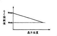
Fig. 2 is the vertical view of an example of the QC predicted value (size change over is poor) of expression the 1st embodiment of the present invention.
Fig. 3 is a routine curve map of the specification of expression the 1st embodiment of the present invention.
Fig. 4 be distribution trend in the wafer of QC predicted value (size change over is poor) of expression the 1st embodiment of the present invention curve map (one of).
Fig. 5 is the curve map (two) of distribution trend in the wafer of QC predicted value (size change over is poor) of expression the 1st embodiment of the present invention.
Fig. 6 is the curve map (three) of distribution trend in the wafer of QC predicted value (size change over is poor) of expression the 1st embodiment of the present invention.
Fig. 7 is the curve map (four) of distribution trend in the wafer of QC predicted value (size change over is poor) of expression the 1st embodiment of the present invention.
Fig. 8 is the curve map (five) of distribution trend in the wafer of QC predicted value (size change over is poor) of expression the 1st embodiment of the present invention.
Fig. 9 is the curve map (six) of distribution trend in the wafer of QC predicted value (size change over is poor) of expression the 1st embodiment of the present invention.
Figure 10 is the complete list of the prescription of expression the 1st embodiment of the present invention.
Figure 11 be used to illustrate the 1st embodiment of the present invention the sampling irradiation area step the wafer synoptic diagram (one of).
Figure 12 is the wafer synoptic diagram (two) of step that is used to illustrate the sampling irradiation area of the 1st embodiment of the present invention.
Figure 13 is the wafer synoptic diagram (three) of step that is used to illustrate the sampling irradiation area of the 1st embodiment of the present invention.
Figure 14 is the wafer synoptic diagram (four) of step that is used to illustrate the sampling irradiation area of the 1st embodiment of the present invention.
Figure 15 is the wafer synoptic diagram (five) of step that is used to illustrate the sampling irradiation area of the 1st embodiment of the present invention.
Figure 16 is the wafer synoptic diagram (six) of step that is used to illustrate the sampling irradiation area of the 1st embodiment of the present invention.
Figure 17 is the table of a part of report of the QC measurement result of expression the 1st embodiment of the present invention.
Figure 18 is the wafer synoptic diagram of a part of report of the QC measurement result of expression the 1st embodiment of the present invention.
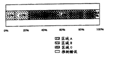
Figure 19 is that the part of report of the QC measurement result of expression the 1st embodiment of the present invention is the curve map of each regional occupation rate.
Figure 20 is that the part of report of the QC measurement result of expression the 1st embodiment of the present invention is the curve map of the aggregate-value of each regional occupation rate.
Figure 21 is that the part of report of the QC measurement result of expression the 1st embodiment of the present invention is the curve map of occupation rate of each prescription of specification zone A.
Figure 22 is that the part of report of the QC measurement result of expression the 1st embodiment of the present invention is the curve map of aggregate-value of occupation rate of each prescription of specification zone A.
Figure 23 is that the part of report of the QC measurement result of expression the 1st embodiment of the present invention is the curve map of occupation rate of each prescription of specification area B.
Figure 24 is that the part of report of the QC measurement result of expression the 1st embodiment of the present invention is the curve map of aggregate-value of occupation rate of each prescription of specification area B.
Figure 25 be the part of report of the QC measurement result of expression the 1st embodiment of the present invention be the QC predicted value batch in the curve map of deviation.
Figure 26 is that the part of report of the QC measurement result of expression the 1st embodiment of the present invention is the curve map of the trend of QC value.
Figure 27 is the process flow diagram of an example of the method for quality control of explanation the 1st embodiment of the present invention.
Figure 28 is the process flow diagram of an example of wafer processing of the lot-to-lot of explanation the 1st embodiment of the present invention.
Figure 29 is the block scheme of an example of the quality control system of explanation the 2nd embodiment of the present invention.
Figure 30 is the curve map of the mahalanobis distance when being used to illustrate the univariate analysis of the 2nd embodiment of the present invention.
Figure 31 is the curve map of the mahalanobis distance when being used to illustrate the multivariable analysis of the 2nd embodiment of the present invention.
Figure 32 is the curve map of trend that is used to illustrate the specification of the 2nd embodiment of the present invention.
Figure 33 is the process flow diagram of an example that is used to illustrate the method for quality control of the 2nd embodiment of the present invention.
Embodiment
Below, with reference to the description of drawings embodiments of the present invention.In the record of the following drawings, give identical or simileys to identical or similar portions.But accompanying drawing is a synoptic diagram.And embodiment shown below is the concrete system and method for implementing technical conceive of the present invention of example, technical conceive of the present invention be not the material, shape, structure, configuration component parts etc. specific be following manner.Technical conceive of the present invention can carry out various changes within the scope of the claims.
(the 1st embodiment)
The quality control system of the 1st embodiment of the present invention possesses as shown in Figure 1: the QC value storage part 22 of storage QC measured value in the past batch; Obtain data acquisition facility 3 in real time as the device internal information of the treating apparatus 10 of batch (hereinafter referred to as " object batch ") of object; The device internal information storage part 21 of memory storage internal information; Storage is according to the prescription storage part 24 of a plurality of prescriptions of the sampling density distributive sorting in the wafer; QC value prediction unit 11, from device internal information storage part 21 and QC value storage part 22 readout device internal informations and QC measured value in the past batch respectively, according to installing internal information and QC measured value, the QC predicted value of forecasting object batch; Wafer determining unit 12 determine to constitute the sample wafer that becomes determination object in a plurality of wafers of object batch according to the QC predicted value; Prescription selected cell 13 is read a plurality of prescriptions from prescription storage part 24, according to the QC predicted value, selects to be applicable to the suitable prescription of sample wafer from a plurality of prescriptions; And determinator 4, use suitable prescription that the wafer that becomes determination object is carried out QC and measure, measurement result is stored in the QC value storage part 22.
In quality control system, central arithmetic processing apparatus (CPU) 1, data storage device 2, data acquisition facility 3, determinator 4, input media 5, output unit 6 and treating apparatus 10 are interconnecting respectively by bus 7.The device group Control Server of the action of CPU1 performance control and treatment device 10 and the illustrated device group of omission and the effect of management server, the running-active status of this management server input description treating apparatus 10 and the device internal information of device parameter (the unit engineering data: the EE data), the operating state of real time monitoring treating apparatus 10.In addition, single CPU 1 has been shown among Fig. 1, but this only is an example, also can has a plurality of CPU, device group Control Server and management servers physically.
Treating apparatus 10 comprises following various semiconductor-fabricating device, for example, ion implantation apparatus, diffusion of contaminants device, form the thermal oxidation apparatus of silicon oxide film (SiO2 film), pile up SiO2 film, phosphorus glass (PSG) film, boron glass (BSG) film, boro-phosphorus glass (BPSG) film, silicon nitride film (Si
3N
4Film), chemical vapor-phase growing (CVD) device of poly-silicon fiml etc., with psg film, bsg film, the annealing device of backflows such as bpsg film (fusing), CVD oxide film etc. is carried out the annealing device of closeization, the annealing device of formation silicide film etc., the sputter equipment of deposit wiring layer, vacuum deposition apparatus, by electroplating the electrolytic plating apparatus that forms metal wiring layer, the cmp on the surface of grinding semiconductor substrate (CMP) device, the dry type of etching semiconductor substrate surface or Wet-type etching device, carry out the cleaning device that resist is removed or solution cleans, the rotation coating unit (spinner) that photoetching treatment is relevant, the exposure device of stepping exposure device etc., cutter sweep is connected to lead wire connecting apparatus on the lead frame etc. to the electrode of shaped like chips semiconductor devices of cutting.The auxiliary device that also can comprise in addition, apparatus for producing pure water, gas cleaning unit etc.And, any form that these semiconductor-fabricating devices can be suitable for how desk-top (バ Star チ) device or separate unit formula (piece ligusticumic formula) are installed.For all embodiments described later, equally also can be suitable for many desktop apparatus or separate unit formula device.
As data acquisition facility 3, can operative installations engineering system (EES) instrument etc.Data acquisition facility 3 individually obtains the device internal information in the processing for the treatment of apparatus 10 in real time, in predetermined timing it is sent to CPU1.As the device internal information, are membrane formation devices, disperser of vacuum flush system for example, when the film stack device has the device of container like that, can enumerate the aperture etc. of valve of temperature, container pressure, gas flow, the pilot-gas flow at temperature, susceptor temperature, a plurality of positions of container outer wall at a plurality of positions in the container at treating apparatus 10.Are dry-etching devices of plasma handling system at treating apparatus 10, when ion implantation apparatus has the device of electrode like that, except that the various parameters of above-mentioned vacuum flush system, matched position, RF power (traveling wave power, reflection wave power), the expression wafer that can also enumerate high frequency (RF) in being batch which wafer position information etc.When treating apparatus 10 is Wet-type etching device, rotation coating unit, exposure device, the lead wire connecting apparatus of atmospheric pressure treatment system, can the enumeration process time, wafer or chip position information etc.
Wafer in the object that 4 pairs of determinators are handled by treating apparatus 10 batch carries out QC and measures.As determinator 4, can use sweep electron microscope (SEM), laser microscope or atomic force microscope microscopes such as (AFM).In addition, also can be the various testing fixtures or the determinator of interfere type film thickness gauge, ellipsometer, contact film thickness gauge, resistance measurement device etc.Determinator 4 for example is determined at the live width Wr of the resist pattern 100 shown in Figure 2 that is formed at wafer in the photo-mask process.In addition, be determined at resist pattern 100 as the live width Wp that is formed at the formed patterns (device pattern) 101 of etched parts in the etching work procedure of mask.As a result, size change over poor (size offset) Wd of the live width Wr of mensuration resist pattern 100 and the live width Wp of formed patterns 101 is as " QC measured value ".A plurality of locating in each wafer measured the QC measured value respectively.
When treating apparatus 10 for example is Etaching device, before and after etch processes, carry out cleaning and drying in the etching chamber (container).According to this dry effect, the parameter change of device internal information is so produce deviation at each batch, each wafer sometimes in the processing before and after dry.For example, as the capacitor locations of the RF match circuit of the parameter of the device internal information of Etaching device, has correlativity with size change over difference Wd shown in Figure 2.That is, when the capacitor locations skew of RF match circuit, the live width Wp of formed patterns 101 change sometimes, size change over difference Wd produces deviation at each batch, each wafer sometimes.
CPU1 shown in Figure 1 possesses: QC value prediction unit 11, wafer determining unit 12, prescription selected cell 13, processing and control element (PCE) 14, report make unit 15, whether qualified identifying unit 16 and abnormality detection classification (FDC) unit 17.QC value prediction unit 11 is read the device internal information in the past in the device internal information storage part 21 that is stored in data storage device 2 and is stored in the QC measured value in the past batch in the QC value storage part 22.QC value prediction unit 11 one side is relevant with reference to the device internal information in the past and the QC measured value of passing by batch, the device internal information of one side during according to the batch processed obtained by data acquisition facility 3, each wafer that constitutes object batch is predicted size change over difference Wd shown in Figure 2 etc. respectively, as " QC predicted value ".That is, the QC predicted value is given a value or a plurality of value to each wafer.For example, situation when giving a plurality of predicted value to wafer refers to following situation etc., promptly, part or all (10%, 20%, 100% etc.) of judging the statistical value (average, maximum, minimum, standard deviation etc.) of a plurality of values, a plurality of values whether more than specification, following situation, the perhaps situation that these values are judged in conjunction with position in the wafer face again etc.In addition, the QC predicted value can also according to batch kind, process conditions etc. predict.
Wafer determining unit 12 judges which side the QC predicted value of each wafer of the formation object batch by 11 predictions of QC value prediction unit belongs in specification zone A, specification area B and the specification zone C shown in Figure 2.When result of determination belongs to specification zone A or specification area B for the QC predicted value, because that specification exceeds probability is bigger, so this wafer is defined as becoming " sample wafer " of determination object.On the other hand, when belonging to the specification zone C since specification to exceed probability less, so at the time point of judging not as determination object.So, after all wafers of object batch is judged, belong to this specification zone C batch in all wafers in be considered to represent that for example wafer of average QC predicted value is defined as sample wafer.That is, 12 pairs of objects of wafer determining unit batch exceed the relatively large wafer of probability to specification as determination object, and specification is exceeded the less relatively wafer of probability, only smaller amounts, for example minimum quantity promptly a wafer as determination object.
Prescription selected cell 13 shown in Figure 1 reads in the QC predicted value of each wafer of the formation object batch in the QC value storage part 22 that is stored in data storage device 2, the QC predicted value of the corresponding sample wafer of being determined by wafer determining unit 12.On the other hand, distribute in the relative wafer face of the anticipation QC predicted value of relevant each sample wafer, according to the device internal information of device internal information, be categorized as for example Fig. 4~pattern shown in Figure 9 in advance to the contribution rate of the QC measured value in past batch and this object batch.
Fig. 4~Fig. 9 is the position of representing wafer with transverse axis, represents the QC predicted value with the longitudinal axis, the curve map of the pattern that distributes in the wafer face of expression QC predicted value.Below, for convenience, the wafer position that is equivalent to end, right side (+side) in the transverse axis of Fig. 4~Fig. 9 is called " wafer right side peripheral part ", the wafer position that is equivalent to (side) end, left side is called " wafer left side peripheral part ".Be distributed in the maximal value Wmax that wafer right side peripheral part has the QC predicted value in the wafer face among Fig. 4, and the QC predicted value reduces monotonously towards the wafer left side.Be distributed in the maximal value Wmax that the wafer central portion has the QC predicted value in the wafer face among Fig. 5, and protruding upward.Distributing in the wafer face among Fig. 6 to present in the identical wafer face distributes, and for example the difference of the maximal value of QC predicted value and minimum value is less than 2nm.Be distributed in the maximal value Wmax that the wafer peripheral part has the QC predicted value in the wafer face among Fig. 7, and protrude downwards.Be distributed in the maximal value Wmax that wafer left side peripheral part has the QC predicted value in the wafer face among Fig. 8, and the QC predicted value reduces monotonously towards the wafer right side.Distribution is distribution at random in the wafer face among Fig. 9, and the difference of the maximal value Wmax of QC predicted value and minimum value Wmin is more than or equal to 2nm.
Distribute in the prescription wafer face of selected cell 13, select in a plurality of prescriptions from be stored in prescription storage part 24 and determine to be applicable to that the QC prescription of the sample wafer of object batch promptly " is suitable for prescription " according to the QC predicted value.In prescription storage part 24 shown in Figure 1, for example shown in Figure 10, storing prescription (1-1)~(1-6), (2-1)~(2-6) and standard prescription etc.Each the pattern classification sampling density that distributes in prescription (1-1)~(1-6), (2-1)~(2-6) and standard prescription the wafer face according to specification zone A~C shown in Figure 3 and Fig. 4~shown in Figure 9.
Figure 11~Figure 16 is the synoptic diagram of example QC prescription, the ellipse representation sample wafer 103 among the figure, and irradiation area 104 is represented in the rectangular area, wherein by the sampled irradiation area of the region representation of blacking.Prescription selected cell 13 shown in Figure 1 selects the specification in the sampling and measuring wafer face to high-density to exceed the suitable prescription of the bigger irradiation area of probability (position).
For example, when the QC predicted value of certain wafer of prediction belongs to specification zone A, according to the suitable prescription of selection from (1-1)~(1-6) prescription group shown in Figure 10 like that of following explanation.Promptly, as shown in Figure 4, in the relative face of the QC predicted value of object batch, distribute towards left side monotone decreasing hour, the specification of the right side peripheral part of wafer exceeds probability and becomes big, is 2 times prescription (1-1) of standard prescription so select the sampling density of the right side peripheral part of the sample wafer 103 shown in the image pattern 11.As shown in Figure 5, when distribution was protruding upward in the face of QC predicted value, the specification of wafer central portion exceeded probability and becomes big, is 2 times prescription (1-2) of standard prescription so select the sampling density of the central portion of the sample wafer 103 shown in the image pattern 12.As shown in Figure 6, in face, distribute when the same, because that the specification in the wafer face exceeds probability is also identical, so select the same prescription (1-3) of the sampling density identical shown in the image pattern 13 with standard prescription.As shown in Figure 7, distribute in the face of QC predicted value when protruding downwards, the specification of wafer peripheral part exceeds probability and becomes big, is 2 times prescription (1-4) of standard prescription so select the sampling density of the peripheral part of the sample wafer 103 shown in the image pattern 14.As shown in Figure 8, towards right side monotone decreasing hour, the specification of the left side peripheral part of wafer exceeds probability and becomes big, is 2 times prescription (1-5) of standard prescription so select the sampling density of the left side peripheral part of the sample wafer 103 shown in the image pattern 15 in the QC predicted value.If distribute in the face at random as shown in Figure 9, then need to strengthen supervision to the wafer All Ranges, be 2 times prescription (1-6) of standard prescription so select sampling density whole in the face as shown in figure 16.
On the other hand, when the QC of certain wafer predicted value is equivalent to the specification area B, from (2-1)~(2-6) prescription group shown in Figure 10, select to be suitable for prescription according to the following stated.Promptly, as shown in Figure 4, distribute in the relative face of QC predicted value towards the right side monotone increasing added-time, the specification of the left side peripheral part of wafer exceeds probability and becomes big, is 2 times prescription (2-1) of standard prescription so select the left side peripheral part of the sample wafer 103 shown in the image pattern 15.Equally as shown in Figure 5, when distribution was protruding upward in the face of QC predicted value, selecting the sampling density of the peripheral part of the sample wafer 103 shown in the image pattern 14 was 2 times prescription (2-2) of standard prescription.As shown in Figure 6, when distribution is identical in wafer face, select the prescription (2-3) identical shown in the image pattern 13 with standard prescription.As shown in Figure 7, if distribute in the face that protrudes downwards, the sampling density of then selecting the central portion of the sample wafer 103 shown in the image pattern 12 is 2 times a prescription (2-4) of standard prescription.As shown in Figure 8, towards the left side monotone increasing added-time, selecting the sampling density of the right side peripheral part of the sample wafer 103 shown in the image pattern 11 is 2 times prescription (2-5) of standard prescription in the QC predicted value.If distribute in the face at random as shown in Figure 9, selecting sampling density whole in the face as shown in figure 16 is 2 times prescription (2-6) of standard prescription.
And, belong to the wafer of specification zone C for the QC predicted value, from these wafers, extract for example wafer of an average QC value of expression, to the standard prescription shown in this wafer selection image pattern 13.In addition, to not inferring that the QC predicted value belongs among the A~C of specification zone which side wafer, choice criteria prescription.
The processing of processing and control element (PCE) 14 control determinators 4 shown in Figure 1.In determinator 4, use suitable prescription (1-1)~(1-6), (2-1)~(2-6) or the standard prescription determined by prescription selected cell 13, as Figure 11~shown in Figure 16, in sample wafer 103, sampling is by the diagram irradiation area 104 of blacking.And, the irradiation area 104 of being taken a sample is carried out QC measure, obtain conducts " QC measured value " such as size change over difference.
Report shown in Figure 1 makes the report that unit 15 makes the expression QC measurement result of Figure 17~shown in Figure 26.In report shown in Figure 17, putting down in writing the project such as prescription title, QC predicted value, QC measured value of the wafer sequence number of all wafers and sample wafer.And, also putting down in writing the QC predicted value of each wafer and desired value p differ from 1 and the QC predicted value d of the QC predicted value of each wafer and the wafer measured in the specification zone C differ from 2.In Figure 18, putting down in writing the interior distribution of wafer face of QC predicted value and the result of determination of the appropriate property that prescription is selected.If trend is roughly consistent with the interior trend classification of the face of device internal information in the face of QC measured value, then be recited as " prescription OK ".If " prescription NG " owing to carried out the selection and the dynamic sampling of wrong prescription, needs change according to trend sorting technique in the face of device internal information supposition.
Each specification zone frequency in the part of Figure 19 and report shown in Figure 20, put down in writing respectively batch and the aggregate-value of each specification zone frequency.Can suitably set arbitrarily during the statistics aggregate-value.In Figure 21 and Figure 22, putting down in writing its QC predicted value according to each batch and be applicable to the frequency of prescription of the wafer that belongs to specification zone A and the aggregate-value of this prescription frequency.In Figure 23 and Figure 24, putting down in writing its QC predicted value according to each batch and be applicable to the frequency of prescription of the wafer that belongs to the specification area B and the aggregate-value of this prescription frequency.In Figure 25, the drawing point of the QC predicted value of all wafers in putting down in writing batch.In Figure 26, putting down in writing desired value and belonging to the QC predicted value of specification zone C and the trend of QC measured value.
Whether qualified identifying unit shown in Figure 1 16 is with reference to the specification management amplitude Wc that is stored in the specification storage part 23, according to the QC measured value judge batch whether qualified.For example, whether qualified identifying unit 16 is when all QC measured values are in specification management amplitude Wc, and is qualified batch being judged to be, if the QC measured value outside the specification management amplitude Wc is arranged, then is judged to be defective.In addition, whether qualified judge also can pass through the visual Figure 17 of operator~report shown in Figure 26, judge according to this report book.FDC unit 17 shown in Figure 1 detects when the QC predicted value extremely departs from specification management amplitude Wc to unusual, and notice output unit etc. has produced unusual situation and unusual type.And, also can export the indication that suspends or force the processing of end process device 10.
And CPU1 has the illustrated memory storage administrative unit of omission.And data storage device 2 between when needing to carry out the input and output of data, carry out necessary file by the memory storage administrative unit and read and write processing.And CPU1 is connecting at input media 5, output unit 6 etc. and is omitting illustrated input-output control unit (interface).As input media 5, for example can use the special input media of keyboard, mouse, OCR recognition devices such as (optical character identification), graphics scanner figures input media, speech input device etc.Management executor (plant manager) can use input media 5 to specify inputoutput data, or specifies the change of the application of using.In addition, also can set the model of analyzing usefulness, can also import the indication of carrying out and stopping computing etc. by input media 5.As output unit 6, can use the display device of LCD or CRT (cathode-ray tube (CRT)) display etc. or printing equipment of ink-jet printer or laser printer etc. etc.Output unit 6 also can show inputoutput data or its analysis result, unusual/normal condition or analytical parameters etc., and plant manager can unify to monitor quality control system.
Below, with reference to the process flow diagram of Figure 27, an example of the method for quality control that has used quality control system shown in Figure 1 is described.
(1), uses the processing of wafers for the treatment of apparatus shown in Figure 1 10 beginning objects batch at step S111.At step S112, the treating apparatus 10 real-time deriving means internal informations of data acquisition facility 3 from technology.The device internal information of being obtained is stored in the device internal information storage part 21 at any time.At step S113, finish processing of wafers.
(2) at step S120, QC value prediction unit 11 is read the device internal information that is stored in the past in the device internal information storage part 21 respectively and is stored in the QC measured value in the past batch in the QC value storage part 22.QC value prediction unit 11 is relevant with reference in the past batch the QC measured value and the device internal information of passing by, device internal information according to the object that obtains by data acquisition facility 3 at step S112 batch, for object batch, according to " the QC predicted value " of each wafer prediction size change over difference Wd for example shown in Figure 2 etc.
(3) at step S130, wafer determining unit 12 is read specification management amplitude Wc shown in Figure 3 from specification storage part 23, and which side each QC predicted value of judging the wafer in the object batch belongs among specification zone A~C of specification management amplitude Wc.When the QC predicted value belongs to specification zone A or specification area B, this wafer is defined as sample wafer, change step S141 or S142 respectively over to.On the other hand, when belonging to the specification zone C, at this time point not this wafer as determination object.Change step S143 over to, wafer determining unit 12 batch in belong to the average device internal information of expression in all wafers of specification zone C a wafer be defined as sample wafer, change step S144 over to.
(4) at step S141, prescription selected cell 13 is read a plurality of prescriptions (with reference to Figure 10) that are stored in the prescription storage part 24, promptly reads a plurality of prescriptions according to the distributive sorting of the sampling density in the wafer.Distribute in the wafer face of prescription selected cell 13 according to Fig. 4~shown in Figure 9, to each sample wafer, specification exceeds the suitable prescription of the bigger irradiation area of probability in the prescription shown in Figure 10 (1-1)~(1-6) of selecting to take a sample to high-density.At step S142, distribute in the wafer face of prescription selected cell 13 according to Fig. 4~shown in Figure 9, specification exceeds the suitable prescription of the bigger irradiation area of probability in the prescription shown in Figure 10 (2-1)~(2-6) of selecting to take a sample to high-density.At step S144, prescription selected cell 13 is selected the standard prescription of uniform sampling in the face, as being applicable to the wafer that belongs to the specification zone C and being detected there is the unusual wafer of QC predicted values such as random deviation in the QC predicted value in wafer face suitable prescription.
(5) at step S150,4 pairs of determinators constitute each sample wafer in a plurality of wafers of object batch, suitable prescription (1-1)~(1-6), (2-1)~(2-6) or the either party in the standard prescription that use is selected by prescription selected cell 13, become the irradiation area of determination object in the sampling wafer face, and carry out the mensuration of QC.Measurement result (QC measured value) is stored in the QC value storage part 22.
(6) at step S160, report make the 15 pairs of objects in unit batch make Figure 17~shown in Figure 26 record the report of QC measurement result etc.The report that is made monitor demonstration by output unit 6 etc. is output.At step S170, if also have next batch, then return the step of step S111, if all batch processed finish, then change step S180 over to.At step S180, whether qualified identifying unit 16 is judged the whether qualified of object batch according to the QC measurement result.Perhaps, also can replace whether qualified identifying unit 16, carry out whether qualifiedly judging according to Figure 17~report shown in Figure 26 by the operator.And, can be not after all batch processed finish, not carry out whether qualifiedly judging yet, and each batch processed is carried out respectively whether qualifiedly judging.
According to the 1st embodiment of the present invention, to the object handled at the device internal information treating apparatus that may change 10 batch, carry out best dynamic sampling, can concentrate thus and measure specification and exceed bigger wafer of probability and irradiation area.Therefore, can reduce because of leaking bad batch of loss that causes.
In addition, the wafer that belongs to the specification zone C for its QC predicted value, only these are belonged to for example wafer in the wafer of specification zone C as the QC determination object, do not need that all wafers is carried out QC and measure, can reduce QC thus and measure needed time and cost.In addition, under the situation that time and cost allow, also can be one or above wafer as determination object.
And, its QC predicted value is belonged to the QC measured value of the wafer that is considered to certified products of specification zone C, the device internal information of correspondence and the related data of QC measured value and device internal information to be stored in the data storage device 2, according to distributing in the face of QC predicted value and the result of determination of the appropriate property that prescription is selected, according to the reliability of each batch check system, can improve the precision of dynamic sampling thus.Therefore, can suppress the yield rate that the dynamic sampling because of mistake causes reduces.
Series of steps shown in Figure 27 can be utilized the algorithm routine with Figure 27 equivalence, controls and carry out quality control system shown in Figure 1.This program can be stored in the program storage device (omitting diagram) of the computer system that constitutes quality control system of the present invention.And this program is by being kept in the computer-readable recording medium, and this recording medium read in the program storage device of quality control system, can carry out the series of steps of embodiments of the present invention.Herein, said " computer-readable recording medium ", for example refer to Jie that the external memory devices, semiconductor memory, disk, CD, photomagneto disk, tape etc. of computing machine can logging program specifically, " computer-readable recording medium " comprises floppy disk, CD-ROM (read-only optical memory), MO (magnetic-light) dish, magnetic tape cassette, open reel tape etc.
For example, the main body of quality control system can constitute medium reading devices such as built-in or outside connection floppy disk and CD drive.By inserting floppy disk to floppy disk from inserting mouth, insert CD-ROM from inserting mouth to CD drive, the read operation that the professional etiquette of going forward side by side is fixed can be installed in the program that is stored in these recording mediums in the program storage device of formation quality control system.And, by connecting the drive assembly of regulation, for example can use utilize in the game package etc. as the ROM of storage arrangement or as the magnetic tape cassette of magnetic tape equipment.In addition, also can be by Information Processing Networks such as the Internets, this procedure stores in program storage device.
Below, use the process flow diagram of Figure 28, an example of the manufacture method (wafer processing of lot-to-lot) of the semiconductor-fabricating device of embodiments of the present invention is described.In addition, the part of manufacturing process only is described in Figure 28, but in the manufacturing process of reality, will passes through not shown a plurality of operations.
(1) at first, at step S0, the wafer in use treating apparatus (for example RIE (reactive ion etching) device) 10 is handled the 1st batch carries out QC then and measures, and resulting QC measured value is stored in the QC value storage part 22.In QC value storage part 22, storing the QC measured value of before the current time, measuring the past that obtains in advance by QC.
(2) at step S1, the wafer in different with the 1st batch the 2nd batch applies resist film on etched parts.At step S2, use photoetching technique to make the resist film patterning, form resist pattern 100 shown in Figure 2 etc.At step S3, use determinator shown in Figure 14 to carry out QC and measure, measure as the preparation quality management, measure the live width Wr of resist pattern 100.The live width Wr of resist pattern 100 is stored in the QC value storage part 22 shown in Figure 1.
(3) at step S4, to the wafer in the 2nd batch, as mask, by having used the RIE for the treatment of apparatus shown in Figure 1 (RIE device) 10, the etched parts of etching and processing form formed patterns 101 shown in Figure 2 etc. the resist film of patterning.At this moment, data acquisition facility 3 obtains the device internal information of the treating apparatus (RIE device) 10 in the 2nd batch the processing in real time.
(4) at step S5, identical with the step of step S130~S180 shown in Figure 27, according to the device internal information in the processing that comprises the 2nd batch the QC measured value in past batch and the 2nd batch that is stored in the QC value storage part 22, predict the 2nd batch QC predicted value, determine sample wafer according to the QC predicted value, according to the QC predicted value, from a plurality of prescriptions of prescription storage part 24, select to be applicable to the suitable prescription of sample wafer, use to be suitable for prescription is measured formed patterns 101 to sample wafer live width Wp.The live width Wp of formed patterns 101 is stored in the QC value storage part 22.Obtain the size change over difference Wd of the live width Wr of the live width Wp of formed patterns 101 and resist pattern 100, according to size change over difference Wd judge the 2nd batch whether qualified.
The wafer processing of lot-to-lot according to the embodiment of the present invention can reduce and leak defective batch, can improve the yield rate of semiconductor-fabricating device.
(the 2nd embodiment)
The quality control system of the 2nd embodiment of the present invention as shown in figure 29, data storage device 2a also has certified products data store 26 and unacceptable product data store 27, CPU1a also has span of management determining unit 18, and these are different with quality control system shown in Figure 1.
Span of management determining unit 18 is determined to handle " span of management " used in the management (SPC) at FDC and statistical." FDC " is as FDC unit 17, constantly handle wafer and implement the supervision for the treatment of apparatus 10 of the part of production process of semiconductor device, before departing from of the treatment conditions for the treatment of apparatus 10 brings harmful effect to the finished product rate, cut off treating apparatus 10, reduce the risk in the wafer manufacturing thus." SPC " carries out statistical treatment according to the huge data of collecting in each checkpoint of manufacturing process, and passing of creating conditions (tendency) in each operation of monitor management and quality of semiconductor devices are passed (tendency)." span of management " is as the threshold value that no abnormal or whether up-to-standard determinating reference is arranged among FDC and the SPC.In FDC and SPC, according to batch the QC measured value in the inboard of span of management the still outside, respectively judgment processing device 10 and handle unusual, batch qualified and defective.
Certified products data store 26 is stored in the device internal information of storing in the device internal information storage part 21, the device internal information (certified products data) when the QC measured value of wafer is judged as in span of management, and the specified quantity that can be stored in the certified products data in the certified products data store 26.Unacceptable product data store 27 is stored in the device internal information of storing in the device internal information storage part 21, the device internal information (unacceptable product data) when the QC measured value of wafer is judged as outside span of management, and the specified quantity that can be stored in the unacceptable product data in the unacceptable product data store 27.
Span of management determining unit 18 is determined and the renewal span of management according to the certified products data and the unacceptable product data that are stored in the unacceptable product data store 27 that are stored in the certified products data store 26.Below, definite step of span of management is described.Calculating is stored in the mean value and the standard deviation of all the certified products data in the certified products data store 26 and is stored in the mean value and the standard deviation of all the unacceptable product data in the unacceptable product data store 27.And, the mahalanobis distance separately of calculating certified products data and unacceptable product data.The mean value of certified products data is made as X
AG, the mean value of unacceptable product data is made as X
ANG, the standard deviation of certified products data is made as σ G, the standard deviation of unacceptable product data is made as σ
NG, obtain the coefficient A that following formula (1) is set up.
Aσ
G+Aσ
NG=|X
ANG-X
AG| ......(1)
And, Figure 30 represents that certified products data and unacceptable product data are univariate situation, Figure 31 represents that certified products data and unacceptable product data are multivariable situation, expression is defined as the threshold value of the bound of regulation span of management with the value Xe of upper/lower positions, this position for example the position that equates of the mahalanobis distance of vial reason amplitude, promptly from the mean value X of certified products data
AGMean value X towards the unacceptable product data
ANGOnly leave σ
GThe position, perhaps from the mean value X of unacceptable product data
ANGMean value X towards the certified products data
AGOnly leave A σ
NGThe position.
And span of management determining unit 18 also can only be determined span of management according to the certified products data.During this situation, mean value (moving average) X that uses the certified products data to obtain
AGAs the center, to this mean value X
AGThe α that adds or deduct standard deviation is two values obtaining of the value of (α for number) arbitrarily doubly, are defined as the threshold value of the bound of regulation management value.That is, span of management is XAG-(α * σ).Shown in figure 32, when carrying out batch processed, upgrade span of management Wc at any time by span of management determining unit 18.Under the relatively strict situation of former span of management Wc, span of management Wc presents and enlarges tendency, but if looser span of management Wc then presents narrow and small tendency.
Below, with reference to the process flow diagram of Figure 33, the method for quality control that has used quality control system shown in Figure 29 is described.
(1), carries out QC according to the step identical and measure with step S111~S180 shown in Figure 27 at step S210.At this moment, whether the QC measured value of judging wafer in the span of management of FDC or SPC, judges that promptly wafer is certified products or unacceptable product.If the QC measured value is in span of management, promptly wafer is certified products, then changes step S211 over to.On the other hand, if the QC measured value outside span of management, promptly wafer is a unacceptable product, then changes step S221 over to.
(2) at step S211, whether the data bulk in the judgement certified products data store 26 is smaller or equal to specified quantity.When decision data quantity surpasses specified quantity, at step S212, the most ancient data in the deletion certified products data store 26.At step S213, up-to-date data storage in certified products data store 26.At step S241, calculate the mean value (moving average) of certified products data, this moving average as the center, determine the α that adds or deduct standard deviation to this mean value doubly the value of (α for number) arbitrarily (value of α * σ) obtain is as the span of management of the threshold value of bound.
(3) at step S211, decision data quantity changes step S212 over to during less than specified quantity, directly the certified products data storage in certified products data store 26.At step S215, calculate the mean value that is stored in the data in the certified products data store 26.At step S216, calculate the standard deviation that is stored in the data in the certified products data store 26.
(4) on the other hand, at step S221, whether the data bulk in the judgement unacceptable product data store 27 is less than specified quantity.When decision data quantity surpasses specified quantity, at step S222, the most ancient data in the deletion unacceptable product data store 27.At step S223, up-to-date data storage in unacceptable product data store 27.When step S221 is judged to be less than specified quantity, change step S224 over to, directly data storage in unacceptable product data store 27.At step S225, calculate the mean value that is stored in the data in the unacceptable product data store 27.At step S226, calculate the standard deviation that is stored in the data in the unacceptable product data store 27.
(5) at step S240, the position the when mahalanobis distance that calculates Figure 30 and certified products data shown in Figure 31 and unacceptable product data equates is determined the span of management of this position as the threshold value of bound.That is, the mean value of certified products data as its central value, is determined described mahalanobis distance 2 times of span of management as its amplitude of absolute value of difference of the mean value of value when equal and certified products data.The span of management of utilization before the span of management that step S241 or S240 determine is upgraded, the up-to-date span of management of use in FDC, SPC etc. next time.
In the past, the span of management of FDC and SPC was utilized the fixed value management, short of change indication, and loose span of management or excessively strict span of management just continue to overuse.Therefore, the leakage of generation unacceptable product is crossed or certified products is judged to be the false declaration of unacceptable product, and produces loss.To this, according to the 2nd embodiment of the present invention, often use up-to-date device internal information, promptly set the span of management of the change of tracking means internal information, thereby even also can be automatically updated into suitable span of management during the state variation for the treatment of apparatus 10.Therefore, can prevent owing to adopt the leakage of the unacceptable product that excessive loose span of management causes and owing to adopt excessively strict span of management to discard the loss that causes normal batch.
In addition, not only use the certified products data, also use unacceptable product data computation mahalanobis distance, and determine to be suitable for the span of management of the differentiation of certified products/unacceptable product, the loss that can reduce further thus that defective batch leakage is crossed and cause because of false declaration.In addition, the position that mahalanobis distance is equated is defined as the threshold value of span of management, but also can from this position to position that certified products data side or unacceptable product data side depart from the threshold value as span of management.
(other embodiments)
As mentioned above, the present invention utilizes the 1st and the 2nd embodiment to record and narrate, but constitute the argumentation of these disclosed parts and accompanying drawing can not be interpreted as be limit of the present invention.Industry personnel certainly obtain various alternate embodiments, embodiment and application technology from the disclosure content.For example, in the 1st and the 2nd above-mentioned embodiment, as shown in Figure 3, be categorized as specification zone A, specification area B, these three zones of specification zone C, but also can be subdivided into the zone more than four, can also select more kinds of prescriptions.And, specification zone A and specification area B form respectively more than or equal to the zone of 10% the value that deducts span of management from the upper specification limit value and smaller or equal to the zone of 10% the value that adds span of management to the specification lower limit, but the critical localisation of specification zone A~C is an example, is not limited to this.And two dimension has been illustrated to distribute in the wafer face in Fig. 4~Fig. 9, but also can use three-dimensional data to select more careful prescription.Like this, the present invention is included in these various embodiments of not putting down in writing etc. certainly.Therefore, technical scope of the present invention only utilizes the specific item of invention of appropriate claim to determine according to above explanation.
Claims (20)
1. quality control system is characterized in that possessing:
Quality management value storage part, storage quality management measured value in the past batch;
Data acquisition facility, obtain processing as object batch the device internal information for the treatment of apparatus;
Device internal information storage part is stored described device internal information;
The prescription storage part, a plurality of prescriptions that the distribution of the sampling density in the memory chip differs from one another;
Quality management value prediction unit, read described device internal information from described device internal information storage part, read the quality management measured value in described past batch from described quality management value storage part, according to described device internal information and described quality management measured value, predict described as object batch the quality management predicted value;
The wafer determining unit, according to described quality management predicted value, determine to constitute described as object batch a plurality of wafers in become the sample wafer of determination object;
The prescription selected cell is read described a plurality of prescription from described prescription storage part, selects to be applicable to the suitable prescription of described sample wafer from described a plurality of prescriptions according to described quality management predicted value; And
Determinator uses described suitable prescription that described sample wafer is carried out quality management and measures, and measurement result is stored in the described quality management value storage part.
2. quality control system according to claim 1 is characterized in that, described wafer determining unit exceeds the relatively large wafer of probability to specification in described a plurality of wafers as described sample wafer.
3. quality control system according to claim 1, it is characterized in that, described prescription selected cell is according to the distribution in the wafer face of described quality management predicted value, specification in the irradiation area in the described sample wafer of taking a sample with relatively large sampling density is exceeded the prescription of the relatively large irradiation area of probability, be chosen as described suitable prescription.
4. quality control system according to claim 1, it is characterized in that, described wafer determining unit is the classification of the quality management predicted value of described wafer appropriate area, the high zone that is higher than described appropriate area that comprises the desired value of described quality management predicted value, the low area that is lower than described appropriate area, and its quality management predicted value is belonged to the wafer of described high zone or low area as described sample wafer.
5. quality control system according to claim 4, it is characterized in that, when described prescription selected cell belongs to described height zone in the quality management predicted value of described sample wafer, the prescription of the higher relatively irradiation area of quality management predicted value in the irradiation area in the described sample wafer of taking a sample with relatively large sampling density, be chosen as described suitable prescription, when the quality management predicted value of described sample wafer belongs to described low area, prescription the relatively low irradiation area of quality management predicted value in the irradiation area in the described sample wafer of taking a sample with relatively large sampling density is chosen as described suitable prescription.
6. quality control system according to claim 1, it is characterized in that described treating apparatus is from comprising that ion implantation apparatus, diffusion of contaminants device, chemical vapor-phase growing apparatus, reflux heat treating apparatus, closeization treating apparatus, silicide form a kind of device of selecting the group of device, sputter equipment, vacuum deposition apparatus, electrolytic plating apparatus, chemical mechanical polishing device, dry-etching device, Wet-type etching device, cleaning device, rotation coating unit, exposure device, cutter sweep and lead wire connecting apparatus.
7. quality control system according to claim 1 is characterized in that, also has the span of management determining unit of determining the span of management of the described quality management measured value of management according to described device internal information.
8. a method for quality control is characterized in that, may further comprise the steps:
Obtain the device internal information for the treatment of apparatus, described treating apparatus handle as object batch,
According to the quality management measured value and the described device internal information in past batch, predict described as object batch the quality management predicted value,
According to described quality management predicted value, determine to constitute described as object batch a plurality of wafers in become the sample wafer of determination object,
According to described quality management predicted value, select to be applicable to the suitable prescription of described sample wafer a plurality of prescriptions that the distribution of the sampling density in wafer differs from one another,
Use described suitable prescription that the described wafer that becomes determination object is carried out quality management and measure, and the storing measurement result.
9. method for quality control according to claim 8, it is characterized in that, described according to described quality management predicted value, determine to constitute described as object batch a plurality of wafers in become in the step of sample wafer of determination object, specification in described a plurality of wafers is exceeded the relatively large wafer of probability as described sample wafer.
10. method for quality control according to claim 8, it is characterized in that, described according to described quality management predicted value, select a plurality of prescriptions that the distribution of the sampling density in wafer differs from one another to be applicable in the step of suitable prescription of described sample wafer, according to the distribution in the wafer face of described quality management predicted value, specification in the irradiation area in the described sample wafer of taking a sample with relatively large sampling density is exceeded the prescription of the relatively large irradiation area of probability, be chosen as described suitable prescription.
11. method for quality control according to claim 8, it is characterized in that, described according to described quality management predicted value, determine to constitute described as object batch a plurality of wafers in become in the step of sample wafer of determination object, is the classification of the quality management predicted value of described wafer appropriate area, the high zone that is higher than described appropriate area that comprises the desired value of described quality management predicted value, the low area that is lower than described appropriate area, and its quality management predicted value is belonged to the wafer of described high zone or low area as described sample wafer.
12. method for quality control according to claim 11, it is characterized in that, described according to described quality management predicted value, select a plurality of prescriptions that the distribution of the sampling density in wafer differs from one another to be applicable in the step of suitable prescription of described sample wafer, when the quality management predicted value of described sample wafer belongs to described height zone, the prescription of the higher relatively irradiation area of quality management predicted value in the irradiation area in the described sample wafer of taking a sample with relatively large sampling density, be chosen as described suitable prescription, when the quality management predicted value of described sample wafer belongs to described low area, prescription the relatively low irradiation area of quality management predicted value in the irradiation area in the described sample wafer of taking a sample with relatively large sampling density is chosen as described suitable prescription.
13. method for quality control according to claim 8 is characterized in that, determines the span of management of the described quality management measured value of management according to described device internal information.
14. the wafer processing of a lot-to-lot is characterized in that, may further comprise the steps:
Use treating apparatus to handle the 1st batch, and store its quality management measured value,
Use described treating apparatus to handle the 2nd batch,
Obtain the device internal information of the described treating apparatus in described the 2nd batch processing,
According to described device internal information in described the 2nd batch processing and described the 1st batch quality management measured value, predict described the 2nd batch quality management measured value,
According to described quality management predicted value, determine to constitute the sample wafer that becomes determination object in described the 2nd batch a plurality of wafers,
According to described quality management predicted value, select to be applicable to the suitable prescription of described sample wafer a plurality of prescriptions that the distribution of the sampling density in wafer differs from one another,
Use described suitable prescription that described sample wafer is carried out quality management and measure,
According to the result that described quality management is measured, judge described the 2nd batch whether qualified.
15. the wafer processing of lot-to-lot according to claim 14 is characterized in that,
The step that described processing is the 2nd batch may further comprise the steps: carries out preliminary treatment to constituting described the 2nd batch all wafers, described all wafers prepared quality management measure, described all wafers is formally handled,
Described according to described device internal information in described the 2nd batch processing and described the 1st batch quality management measured value, the step of predicting described the 2nd batch quality management measured value comprises: according to described before the 1st batch batch the quality management measured value and described described all wafers is prepared the result that quality management is measured, predict described the 2nd batch quality management predicted value.
16. the wafer processing of lot-to-lot according to claim 14, it is characterized in that, described according to described quality management predicted value, determine to constitute in the step of the sample wafer that becomes determination object in described the 2nd batch a plurality of wafers, specification in described a plurality of wafers is exceeded the relatively large wafer of probability as described sample wafer.
17. the wafer processing of lot-to-lot according to claim 14, it is characterized in that, described according to described quality management predicted value, select a plurality of prescriptions that the distribution of the sampling density in wafer differs from one another to be applicable in the step of suitable prescription of described sample wafer, according to the distribution in the wafer face of described quality management predicted value, specification in the irradiation area in the described sample wafer of taking a sample with relatively large sampling density is exceeded the prescription of the relatively large irradiation area of probability, be chosen as described suitable prescription.
18. the wafer processing of lot-to-lot according to claim 14, it is characterized in that, described according to described quality management predicted value, determine to constitute in the step of the sample wafer that becomes determination object in described the 2nd batch a plurality of wafers, is the classification of the quality management predicted value of described wafer appropriate area, the high zone that is higher than described appropriate area that comprises the desired value of described quality management predicted value, the low area that is lower than described appropriate area, and its quality management predicted value is belonged to the wafer of described high zone or low area as described sample wafer.
19. the wafer processing of lot-to-lot according to claim 18, it is characterized in that, described according to described quality management predicted value, select a plurality of prescriptions that the distribution of the sampling density in wafer differs from one another to be applicable in the step of suitable prescription of described sample wafer, when the quality management predicted value of described sample wafer belongs to described height zone, the prescription of the higher relatively irradiation area of quality management predicted value in the irradiation area in the described sample wafer of taking a sample with relatively large sampling density, be chosen as described suitable prescription, when the quality management predicted value of described sample wafer belongs to described low area, prescription the relatively low irradiation area of quality management predicted value in the irradiation area in the described sample wafer of taking a sample with relatively large sampling density is chosen as described suitable prescription.
20. the wafer processing of lot-to-lot according to claim 14 is characterized in that, further determines the span of management of the described quality management measured value of management according to described device internal information.
Applications Claiming Priority (2)
| Application Number | Priority Date | Filing Date | Title |
|---|---|---|---|
| JP109209/2005 | 2005-04-05 | ||
| JP2005109209A JP4693464B2 (en) | 2005-04-05 | 2005-04-05 | Quality control system, quality control method and lot-by-lot wafer processing method |
Publications (2)
| Publication Number | Publication Date |
|---|---|
| CN1848006A CN1848006A (en) | 2006-10-18 |
| CN100424599C true CN100424599C (en) | 2008-10-08 |
Family
ID=37077600
Family Applications (1)
| Application Number | Title | Priority Date | Filing Date |
|---|---|---|---|
| CNB200610066598XA Expired - Fee Related CN100424599C (en) | 2005-04-05 | 2006-04-03 | Quality control system, quality control method, and method of lot-to-lot wafer processing |
Country Status (4)
| Country | Link |
|---|---|
| US (1) | US7463941B2 (en) |
| JP (1) | JP4693464B2 (en) |
| CN (1) | CN100424599C (en) |
| TW (1) | TW200643669A (en) |
Cited By (1)
| Publication number | Priority date | Publication date | Assignee | Title |
|---|---|---|---|---|
| CN104794318A (en) * | 2014-01-17 | 2015-07-22 | 无锡华润上华半导体有限公司 | Data processing method for establishing semiconductor device statistical model |
Families Citing this family (29)
| Publication number | Priority date | Publication date | Assignee | Title |
|---|---|---|---|---|
| US8041440B2 (en) * | 2006-07-13 | 2011-10-18 | Taiwan Semiconductor Manufacturing Company, Ltd. | Method and system for providing a selection of golden tools for better defect density and product yield |
| JP2008121447A (en) * | 2006-11-09 | 2008-05-29 | Nissan Diesel Motor Co Ltd | Fuel injection control device |
| JPWO2008075404A1 (en) * | 2006-12-19 | 2010-04-02 | 株式会社システムブイマネジメント | Semiconductor manufacturing system |
| JP5169096B2 (en) * | 2007-09-14 | 2013-03-27 | Jfeスチール株式会社 | Quality prediction apparatus, quality prediction method, and product manufacturing method |
| JP5169098B2 (en) * | 2007-09-14 | 2013-03-27 | Jfeスチール株式会社 | Quality prediction apparatus, quality prediction method and manufacturing method |
| US7962440B2 (en) * | 2007-09-27 | 2011-06-14 | Rockwell Automation Technologies, Inc. | Adaptive industrial systems via embedded historian data |
| US8002871B2 (en) * | 2008-02-01 | 2011-08-23 | Honeywell International Inc. | Methods and apparatus for an oxygen furnace quality control system |
| US7974723B2 (en) * | 2008-03-06 | 2011-07-05 | Applied Materials, Inc. | Yield prediction feedback for controlling an equipment engineering system |
| US7974802B2 (en) * | 2008-03-07 | 2011-07-05 | International Business Machines Corporation | Photomask image inspection |
| JP2009257922A (en) * | 2008-04-16 | 2009-11-05 | Jatco Ltd | Inspection method for automatic transmission and inspection apparatus for automatic transmission |
| WO2010137488A1 (en) * | 2009-05-29 | 2010-12-02 | 株式会社村田製作所 | Product inspection device, product inspection method, and computer program |
| CN102448626B (en) * | 2009-05-29 | 2013-12-04 | 株式会社村田制作所 | Product sorting device, product sorting method |
| US8437870B2 (en) * | 2009-06-05 | 2013-05-07 | Taiwan Semiconductor Manufacturing Company, Ltd. | System and method for implementing a virtual metrology advanced process control platform |
| JP5503564B2 (en) * | 2011-01-18 | 2014-05-28 | 東京エレクトロン株式会社 | Abnormality determination system for processing apparatus and abnormality determination method thereof |
| JP5855841B2 (en) | 2011-04-01 | 2016-02-09 | 株式会社日立国際電気 | Management device |
| NL2009853A (en) * | 2011-12-23 | 2013-06-26 | Asml Netherlands Bv | Methods and apparatus for measuring a property of a substrate. |
| JP5783975B2 (en) | 2012-08-29 | 2015-09-24 | 株式会社東芝 | Semiconductor manufacturing processing system and method |
| US20150253762A1 (en) * | 2012-09-26 | 2015-09-10 | Hitachi Kokusai Electric Inc. | Integrated management system, management device, method of displaying information for substrate processing apparatus, and recording medium |
| CN110490458A (en) | 2013-03-20 | 2019-11-22 | 生活时间品牌公司 | A kind of moving mass control inspection system |
| WO2015029777A1 (en) | 2013-08-28 | 2015-03-05 | 堺ディスプレイプロダクト株式会社 | Plasma processing device and method for monitoring plasma processing device |
| CN105470156B (en) * | 2014-09-09 | 2018-09-04 | 中芯国际集成电路制造(上海)有限公司 | A kind of measurement technique based on RTD |
| JP6178768B2 (en) * | 2014-09-17 | 2017-08-09 | 株式会社東芝 | Quality control device and management method thereof |
| JP6385914B2 (en) * | 2015-12-16 | 2018-09-05 | 三菱重工業株式会社 | Quality monitoring system and quality monitoring method |
| JP6453805B2 (en) * | 2016-04-25 | 2019-01-16 | ファナック株式会社 | Production system for setting judgment values for variables related to product abnormalities |
| CN110246775B (en) * | 2018-03-09 | 2022-05-03 | 联华电子股份有限公司 | Apparatus and method for controlling operation of machine |
| US11335607B2 (en) | 2020-07-09 | 2022-05-17 | Tokyo Electron Limited | Apparatus and methods for wafer to wafer bonding |
| CN114198878B (en) * | 2020-09-17 | 2023-08-04 | 青岛海信电子产业控股股份有限公司 | Air quality adjusting method and intelligent equipment |
| US20230258585A1 (en) * | 2022-02-16 | 2023-08-17 | Kla Corporation | Semiconductor Measurements With Robust In-Line Tool Matching |
| CN115881529B (en) * | 2023-02-06 | 2023-05-12 | 合肥新晶集成电路有限公司 | Wet etching method, device, system, computer equipment and medium |
Citations (6)
| Publication number | Priority date | Publication date | Assignee | Title |
|---|---|---|---|---|
| CN1223393A (en) * | 1998-01-14 | 1999-07-21 | 三星电子株式会社 | Method for controlling process conditions of semiconductor fabricating equipments management system |
| US5930137A (en) * | 1995-11-24 | 1999-07-27 | Nec Corporation | Work supplying method and apparatus to batch process apparatus for semiconductor wafer with preferential treatment to time critical lots |
| JP2002343753A (en) * | 2001-05-21 | 2002-11-29 | Nikon Corp | Simulation method and apparatus thereof, machining apparatus, machining system, and semiconductor device manufacturing method |
| US20020193899A1 (en) * | 2001-06-19 | 2002-12-19 | Applied Materials, Inc. | Dynamic metrology schemes and sampling schemes for advanced process control in semiconductor processing |
| US20050004773A1 (en) * | 2002-12-31 | 2005-01-06 | Hung-En Tai | Method for analyzing in-line qc test parameters |
| US20050010319A1 (en) * | 2003-07-09 | 2005-01-13 | Sukesh Patel | System and method for validating and visualizing APC assisted semiconductor manufacturing processes |
Family Cites Families (12)
| Publication number | Priority date | Publication date | Assignee | Title |
|---|---|---|---|---|
| JPH07244694A (en) | 1994-03-04 | 1995-09-19 | Fujitsu Ltd | Quality control device |
| US5629772A (en) * | 1994-12-20 | 1997-05-13 | International Business Machines Corporation | Monitoring of minimum features on a substrate |
| US6408219B2 (en) * | 1998-05-11 | 2002-06-18 | Applied Materials, Inc. | FAB yield enhancement system |
| JP3926478B2 (en) * | 1998-06-01 | 2007-06-06 | 株式会社ルネサステクノロジ | Semiconductor manufacturing method |
| JP4071449B2 (en) * | 2001-03-27 | 2008-04-02 | 株式会社東芝 | Sensor abnormality detection method and sensor abnormality detection device |
| JP4184638B2 (en) * | 2001-08-31 | 2008-11-19 | 株式会社東芝 | Life diagnosis method for semiconductor manufacturing equipment |
| US6687561B1 (en) * | 2002-04-03 | 2004-02-03 | Advanced Micro Devices, Inc. | Method and apparatus for determining a sampling plan based on defectivity |
| JP3834546B2 (en) * | 2002-12-13 | 2006-10-18 | 株式会社東芝 | Measuring object pattern selection method, pattern inspection method, semiconductor device manufacturing method, program, and pattern inspection apparatus |
| US8017411B2 (en) * | 2002-12-18 | 2011-09-13 | GlobalFoundries, Inc. | Dynamic adaptive sampling rate for model prediction |
| JP3699960B2 (en) * | 2003-03-14 | 2005-09-28 | 株式会社東芝 | Inspection recipe creation system, defect review system, inspection recipe creation method and defect review method |
| US6947805B1 (en) * | 2003-08-04 | 2005-09-20 | Advanced Micro Devices, Inc. | Dynamic metrology sampling techniques for identified lots, and system for performing same |
| JP4008899B2 (en) * | 2003-09-08 | 2007-11-14 | 株式会社東芝 | Semiconductor device manufacturing system and semiconductor device manufacturing method |
-
2005
- 2005-04-05 JP JP2005109209A patent/JP4693464B2/en not_active Expired - Fee Related
-
2006
- 2006-03-08 TW TW095107769A patent/TW200643669A/en not_active IP Right Cessation
- 2006-04-03 CN CNB200610066598XA patent/CN100424599C/en not_active Expired - Fee Related
- 2006-04-03 US US11/395,276 patent/US7463941B2/en not_active Expired - Fee Related
Patent Citations (6)
| Publication number | Priority date | Publication date | Assignee | Title |
|---|---|---|---|---|
| US5930137A (en) * | 1995-11-24 | 1999-07-27 | Nec Corporation | Work supplying method and apparatus to batch process apparatus for semiconductor wafer with preferential treatment to time critical lots |
| CN1223393A (en) * | 1998-01-14 | 1999-07-21 | 三星电子株式会社 | Method for controlling process conditions of semiconductor fabricating equipments management system |
| JP2002343753A (en) * | 2001-05-21 | 2002-11-29 | Nikon Corp | Simulation method and apparatus thereof, machining apparatus, machining system, and semiconductor device manufacturing method |
| US20020193899A1 (en) * | 2001-06-19 | 2002-12-19 | Applied Materials, Inc. | Dynamic metrology schemes and sampling schemes for advanced process control in semiconductor processing |
| US20050004773A1 (en) * | 2002-12-31 | 2005-01-06 | Hung-En Tai | Method for analyzing in-line qc test parameters |
| US20050010319A1 (en) * | 2003-07-09 | 2005-01-13 | Sukesh Patel | System and method for validating and visualizing APC assisted semiconductor manufacturing processes |
Cited By (2)
| Publication number | Priority date | Publication date | Assignee | Title |
|---|---|---|---|---|
| CN104794318A (en) * | 2014-01-17 | 2015-07-22 | 无锡华润上华半导体有限公司 | Data processing method for establishing semiconductor device statistical model |
| CN104794318B (en) * | 2014-01-17 | 2017-11-21 | 无锡华润上华科技有限公司 | For establishing the data processing method of semiconductor devices statistical model |
Also Published As
| Publication number | Publication date |
|---|---|
| JP2006293433A (en) | 2006-10-26 |
| US20060235560A1 (en) | 2006-10-19 |
| US7463941B2 (en) | 2008-12-09 |
| TWI320518B (en) | 2010-02-11 |
| CN1848006A (en) | 2006-10-18 |
| JP4693464B2 (en) | 2011-06-01 |
| TW200643669A (en) | 2006-12-16 |
Similar Documents
| Publication | Publication Date | Title |
|---|---|---|
| CN100424599C (en) | Quality control system, quality control method, and method of lot-to-lot wafer processing | |
| JP2008004641A (en) | Defect detection system, defect detection method, and program | |
| CN101032013B (en) | Method and system for dynamically adjusting metrology sampling based upon available metrology capacity | |
| US7248939B1 (en) | Method and apparatus for multivariate fault detection and classification | |
| JP2003100825A (en) | Method for producing semiconductor device and defect inspecting data processing method and system | |
| US8396583B2 (en) | Method and system for implementing virtual metrology in semiconductor fabrication | |
| CN100523839C (en) | Metrology tool error log analysis methodology and system | |
| US6614050B1 (en) | Semiconductor manufacturing apparatus | |
| US6563300B1 (en) | Method and apparatus for fault detection using multiple tool error signals | |
| US20030000922A1 (en) | Using scatterometry to develop real time etch image | |
| US6687561B1 (en) | Method and apparatus for determining a sampling plan based on defectivity | |
| JP3175765B2 (en) | Inspection method for semiconductor wafer | |
| CN103137513A (en) | Integrated circuit manufacturing tool condition monitoring system and method | |
| TWI614699B (en) | Product quality prediction method for mass customization | |
| US7337034B1 (en) | Method and apparatus for determining a root cause of a statistical process control failure | |
| TW201921541A (en) | Improving defect location accuracy using shape based grouping guided defect centering | |
| US6821792B1 (en) | Method and apparatus for determining a sampling plan based on process and equipment state information | |
| TWI280603B (en) | Manufacturing system of semiconductor device and manufacturing method of semiconductor device | |
| US6754593B1 (en) | Method and apparatus for measuring defects | |
| US6771356B1 (en) | Scatterometry of grating structures to monitor wafer stress | |
| JP4480482B2 (en) | Plasma etching processing apparatus control method and trimming amount control system | |
| JP2012227282A (en) | Processing device and processing condition calculation method | |
| US20040088068A1 (en) | Method and apparatus for providing first-principles feed-forward manufacturing control | |
| CN101002150A (en) | Method and system for prioritizing material to clear exception conditions | |
| JP4524720B2 (en) | Process control device |
Legal Events
| Date | Code | Title | Description |
|---|---|---|---|
| C06 | Publication | ||
| PB01 | Publication | ||
| C10 | Entry into substantive examination | ||
| SE01 | Entry into force of request for substantive examination | ||
| C14 | Grant of patent or utility model | ||
| GR01 | Patent grant | ||
| C17 | Cessation of patent right | ||
| CF01 | Termination of patent right due to non-payment of annual fee |
Granted publication date: 20081008 |