CN100501910C - Manufacturing method for a base piece made to adhere to an adhesive sheet, for a semiconductor wafer and for a semiconductor device - Google Patents
Manufacturing method for a base piece made to adhere to an adhesive sheet, for a semiconductor wafer and for a semiconductor device Download PDFInfo
- Publication number
- CN100501910C CN100501910C CNB2005100896161A CN200510089616A CN100501910C CN 100501910 C CN100501910 C CN 100501910C CN B2005100896161 A CNB2005100896161 A CN B2005100896161A CN 200510089616 A CN200510089616 A CN 200510089616A CN 100501910 C CN100501910 C CN 100501910C
- Authority
- CN
- China
- Prior art keywords
- thin slice
- adhesion
- mentioned
- adhesion thin
- glass basis
- Prior art date
- Legal status (The legal status is an assumption and is not a legal conclusion. Google has not performed a legal analysis and makes no representation as to the accuracy of the status listed.)
- Expired - Fee Related
Links
- 239000004065 semiconductor Substances 0.000 title claims description 69
- 238000004519 manufacturing process Methods 0.000 title claims description 41
- 239000000853 adhesive Substances 0.000 title abstract 9
- 230000001070 adhesive effect Effects 0.000 title abstract 9
- 239000011521 glass Substances 0.000 claims abstract description 68
- 238000000034 method Methods 0.000 claims abstract description 42
- 239000002184 metal Substances 0.000 claims description 46
- 238000005406 washing Methods 0.000 claims description 4
- 239000011248 coating agent Substances 0.000 claims description 3
- 238000000576 coating method Methods 0.000 claims description 3
- 238000004140 cleaning Methods 0.000 claims 3
- 239000006210 lotion Substances 0.000 claims 3
- 238000005520 cutting process Methods 0.000 abstract description 3
- 239000005357 flat glass Substances 0.000 description 59
- 239000011159 matrix material Substances 0.000 description 39
- 235000012431 wafers Nutrition 0.000 description 27
- 230000000903 blocking effect Effects 0.000 description 15
- 239000000428 dust Substances 0.000 description 13
- XUIMIQQOPSSXEZ-UHFFFAOYSA-N Silicon Chemical compound [Si] XUIMIQQOPSSXEZ-UHFFFAOYSA-N 0.000 description 7
- 229910052710 silicon Inorganic materials 0.000 description 7
- 239000010703 silicon Substances 0.000 description 7
- 230000002950 deficient Effects 0.000 description 6
- 239000000758 substrate Substances 0.000 description 6
- 239000003463 adsorbent Substances 0.000 description 5
- 238000010521 absorption reaction Methods 0.000 description 3
- 238000004026 adhesive bonding Methods 0.000 description 3
- XLYOFNOQVPJJNP-UHFFFAOYSA-N water Substances O XLYOFNOQVPJJNP-UHFFFAOYSA-N 0.000 description 3
- IJGRMHOSHXDMSA-UHFFFAOYSA-N Atomic nitrogen Chemical compound N#N IJGRMHOSHXDMSA-UHFFFAOYSA-N 0.000 description 2
- VYPSYNLAJGMNEJ-UHFFFAOYSA-N Silicium dioxide Chemical compound O=[Si]=O VYPSYNLAJGMNEJ-UHFFFAOYSA-N 0.000 description 2
- 239000003599 detergent Substances 0.000 description 2
- 238000005516 engineering process Methods 0.000 description 2
- 230000001681 protective effect Effects 0.000 description 2
- 238000001179 sorption measurement Methods 0.000 description 2
- 230000015572 biosynthetic process Effects 0.000 description 1
- 230000000694 effects Effects 0.000 description 1
- 239000007789 gas Substances 0.000 description 1
- 239000000543 intermediate Substances 0.000 description 1
- 230000014759 maintenance of location Effects 0.000 description 1
- 229910052757 nitrogen Inorganic materials 0.000 description 1
- 238000005240 physical vapour deposition Methods 0.000 description 1
- 239000000377 silicon dioxide Substances 0.000 description 1
- 230000003068 static effect Effects 0.000 description 1
- 238000003860 storage Methods 0.000 description 1
Images


Classifications
-
- H—ELECTRICITY
- H01—ELECTRIC ELEMENTS
- H01L—SEMICONDUCTOR DEVICES NOT COVERED BY CLASS H10
- H01L21/00—Processes or apparatus adapted for the manufacture or treatment of semiconductor or solid state devices or of parts thereof
- H01L21/70—Manufacture or treatment of devices consisting of a plurality of solid state components formed in or on a common substrate or of parts thereof; Manufacture of integrated circuit devices or of parts thereof
- H01L21/77—Manufacture or treatment of devices consisting of a plurality of solid state components or integrated circuits formed in, or on, a common substrate
- H01L21/78—Manufacture or treatment of devices consisting of a plurality of solid state components or integrated circuits formed in, or on, a common substrate with subsequent division of the substrate into plural individual devices
-
- H—ELECTRICITY
- H01—ELECTRIC ELEMENTS
- H01L—SEMICONDUCTOR DEVICES NOT COVERED BY CLASS H10
- H01L27/00—Devices consisting of a plurality of semiconductor or other solid-state components formed in or on a common substrate
- H01L27/14—Devices consisting of a plurality of semiconductor or other solid-state components formed in or on a common substrate including semiconductor components sensitive to infrared radiation, light, electromagnetic radiation of shorter wavelength or corpuscular radiation and specially adapted either for the conversion of the energy of such radiation into electrical energy or for the control of electrical energy by such radiation
- H01L27/144—Devices controlled by radiation
- H01L27/146—Imager structures
- H01L27/14601—Structural or functional details thereof
- H01L27/14618—Containers
-
- H—ELECTRICITY
- H01—ELECTRIC ELEMENTS
- H01L—SEMICONDUCTOR DEVICES NOT COVERED BY CLASS H10
- H01L21/00—Processes or apparatus adapted for the manufacture or treatment of semiconductor or solid state devices or of parts thereof
- H01L21/67—Apparatus specially adapted for handling semiconductor or electric solid state devices during manufacture or treatment thereof; Apparatus specially adapted for handling wafers during manufacture or treatment of semiconductor or electric solid state devices or components ; Apparatus not specifically provided for elsewhere
- H01L21/683—Apparatus specially adapted for handling semiconductor or electric solid state devices during manufacture or treatment thereof; Apparatus specially adapted for handling wafers during manufacture or treatment of semiconductor or electric solid state devices or components ; Apparatus not specifically provided for elsewhere for supporting or gripping
- H01L21/6835—Apparatus specially adapted for handling semiconductor or electric solid state devices during manufacture or treatment thereof; Apparatus specially adapted for handling wafers during manufacture or treatment of semiconductor or electric solid state devices or components ; Apparatus not specifically provided for elsewhere for supporting or gripping using temporarily an auxiliary support
-
- H—ELECTRICITY
- H01—ELECTRIC ELEMENTS
- H01L—SEMICONDUCTOR DEVICES NOT COVERED BY CLASS H10
- H01L23/00—Details of semiconductor or other solid state devices
- H01L23/02—Containers; Seals
-
- H—ELECTRICITY
- H01—ELECTRIC ELEMENTS
- H01L—SEMICONDUCTOR DEVICES NOT COVERED BY CLASS H10
- H01L2221/00—Processes or apparatus adapted for the manufacture or treatment of semiconductor or solid state devices or of parts thereof covered by H01L21/00
- H01L2221/67—Apparatus for handling semiconductor or electric solid state devices during manufacture or treatment thereof; Apparatus for handling wafers during manufacture or treatment of semiconductor or electric solid state devices or components; Apparatus not specifically provided for elsewhere
- H01L2221/683—Apparatus for handling semiconductor or electric solid state devices during manufacture or treatment thereof; Apparatus for handling wafers during manufacture or treatment of semiconductor or electric solid state devices or components; Apparatus not specifically provided for elsewhere for supporting or gripping
- H01L2221/68304—Apparatus for handling semiconductor or electric solid state devices during manufacture or treatment thereof; Apparatus for handling wafers during manufacture or treatment of semiconductor or electric solid state devices or components; Apparatus not specifically provided for elsewhere for supporting or gripping using temporarily an auxiliary support
- H01L2221/68327—Apparatus for handling semiconductor or electric solid state devices during manufacture or treatment thereof; Apparatus for handling wafers during manufacture or treatment of semiconductor or electric solid state devices or components; Apparatus not specifically provided for elsewhere for supporting or gripping using temporarily an auxiliary support used during dicing or grinding
- H01L2221/68331—Apparatus for handling semiconductor or electric solid state devices during manufacture or treatment thereof; Apparatus for handling wafers during manufacture or treatment of semiconductor or electric solid state devices or components; Apparatus not specifically provided for elsewhere for supporting or gripping using temporarily an auxiliary support used during dicing or grinding of passive members, e.g. die mounting substrate
-
- H—ELECTRICITY
- H01—ELECTRIC ELEMENTS
- H01L—SEMICONDUCTOR DEVICES NOT COVERED BY CLASS H10
- H01L2221/00—Processes or apparatus adapted for the manufacture or treatment of semiconductor or solid state devices or of parts thereof covered by H01L21/00
- H01L2221/67—Apparatus for handling semiconductor or electric solid state devices during manufacture or treatment thereof; Apparatus for handling wafers during manufacture or treatment of semiconductor or electric solid state devices or components; Apparatus not specifically provided for elsewhere
- H01L2221/683—Apparatus for handling semiconductor or electric solid state devices during manufacture or treatment thereof; Apparatus for handling wafers during manufacture or treatment of semiconductor or electric solid state devices or components; Apparatus not specifically provided for elsewhere for supporting or gripping
- H01L2221/68304—Apparatus for handling semiconductor or electric solid state devices during manufacture or treatment thereof; Apparatus for handling wafers during manufacture or treatment of semiconductor or electric solid state devices or components; Apparatus not specifically provided for elsewhere for supporting or gripping using temporarily an auxiliary support
- H01L2221/68368—Apparatus for handling semiconductor or electric solid state devices during manufacture or treatment thereof; Apparatus for handling wafers during manufacture or treatment of semiconductor or electric solid state devices or components; Apparatus not specifically provided for elsewhere for supporting or gripping using temporarily an auxiliary support used in a transfer process involving at least two transfer steps, i.e. including an intermediate handle substrate
-
- H—ELECTRICITY
- H01—ELECTRIC ELEMENTS
- H01L—SEMICONDUCTOR DEVICES NOT COVERED BY CLASS H10
- H01L27/00—Devices consisting of a plurality of semiconductor or other solid-state components formed in or on a common substrate
- H01L27/14—Devices consisting of a plurality of semiconductor or other solid-state components formed in or on a common substrate including semiconductor components sensitive to infrared radiation, light, electromagnetic radiation of shorter wavelength or corpuscular radiation and specially adapted either for the conversion of the energy of such radiation into electrical energy or for the control of electrical energy by such radiation
- H01L27/144—Devices controlled by radiation
- H01L27/146—Imager structures
- H01L27/14601—Structural or functional details thereof
- H01L27/14625—Optical elements or arrangements associated with the device
- H01L27/14627—Microlenses
-
- H—ELECTRICITY
- H01—ELECTRIC ELEMENTS
- H01L—SEMICONDUCTOR DEVICES NOT COVERED BY CLASS H10
- H01L27/00—Devices consisting of a plurality of semiconductor or other solid-state components formed in or on a common substrate
- H01L27/14—Devices consisting of a plurality of semiconductor or other solid-state components formed in or on a common substrate including semiconductor components sensitive to infrared radiation, light, electromagnetic radiation of shorter wavelength or corpuscular radiation and specially adapted either for the conversion of the energy of such radiation into electrical energy or for the control of electrical energy by such radiation
- H01L27/144—Devices controlled by radiation
- H01L27/146—Imager structures
- H01L27/148—Charge coupled imagers
-
- H—ELECTRICITY
- H01—ELECTRIC ELEMENTS
- H01L—SEMICONDUCTOR DEVICES NOT COVERED BY CLASS H10
- H01L2924/00—Indexing scheme for arrangements or methods for connecting or disconnecting semiconductor or solid-state bodies as covered by H01L24/00
- H01L2924/0001—Technical content checked by a classifier
- H01L2924/0002—Not covered by any one of groups H01L24/00, H01L24/00 and H01L2224/00
-
- H—ELECTRICITY
- H01—ELECTRIC ELEMENTS
- H01L—SEMICONDUCTOR DEVICES NOT COVERED BY CLASS H10
- H01L2924/00—Indexing scheme for arrangements or methods for connecting or disconnecting semiconductor or solid-state bodies as covered by H01L24/00
- H01L2924/15—Details of package parts other than the semiconductor or other solid state devices to be connected
- H01L2924/161—Cap
- H01L2924/162—Disposition
- H01L2924/16235—Connecting to a semiconductor or solid-state bodies, i.e. cap-to-chip
-
- H—ELECTRICITY
- H01—ELECTRIC ELEMENTS
- H01L—SEMICONDUCTOR DEVICES NOT COVERED BY CLASS H10
- H01L2924/00—Indexing scheme for arrangements or methods for connecting or disconnecting semiconductor or solid-state bodies as covered by H01L24/00
- H01L2924/30—Technical effects
- H01L2924/301—Electrical effects
- H01L2924/3025—Electromagnetic shielding
-
- Y—GENERAL TAGGING OF NEW TECHNOLOGICAL DEVELOPMENTS; GENERAL TAGGING OF CROSS-SECTIONAL TECHNOLOGIES SPANNING OVER SEVERAL SECTIONS OF THE IPC; TECHNICAL SUBJECTS COVERED BY FORMER USPC CROSS-REFERENCE ART COLLECTIONS [XRACs] AND DIGESTS
- Y10—TECHNICAL SUBJECTS COVERED BY FORMER USPC
- Y10T—TECHNICAL SUBJECTS COVERED BY FORMER US CLASSIFICATION
- Y10T156/00—Adhesive bonding and miscellaneous chemical manufacture
- Y10T156/10—Methods of surface bonding and/or assembly therefor
- Y10T156/1052—Methods of surface bonding and/or assembly therefor with cutting, punching, tearing or severing
Abstract
A first adhesive sheet is made to adhere to glass in plate form, and after that, the glass is cut with a blade so as to be separated into a number of glass pieces. A second adhesive sheet is made to adhere to the surfaces of glass pieces on the side opposite to the surface to which the first adhesive sheet is made to adhere. The first adhesive sheet is peeled from the glass pieces. The first adhesive sheet is peeled in the state where glass chips that have been created in the process for cutting the glass adhere to the first adhesive sheet, and therefore, most of the glass chips which adhere to the first adhesive sheet are removed with the respective glass pieces in the state of adhering to the second adhesive sheet not being scattered.
Description
Technical field
The present invention relates to make the method that sticks on a plurality of base sheets such as for example sheet glass, silica-based plate etc. on the adhesion thin slice, relate to the manufacture method and the manufacturing method for semiconductor device of the semiconductor wafer that utilizes this manufacture method that sticks on the base sheet on the adhesion thin slice simultaneously.
Background technology
Disclose by sticking glass make the chip of cover wafers state each imageing sensor, separate each chip, prevent because the technology of adhering to of the damage that causes of defective in the imageing sensor or dust (for example opening flat 3-No. 151666 communiques) with reference to the spy.But how the scutellate glass of pasting on the spy opens in flat 3-No. 151666 communiques about imageing sensor portion is made, and does not do any explanation.
The manufacture method (for example opening flat 5-No. 41461 communiques with reference to the spy) of the sheet glass that uses as the cover section of equipping on the assembly of the semiconductor element of light accepting parts such as the semiconductor element (EPROM) of the memory with available ultraviolet write/erase or CCD has been proposed in addition.
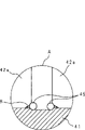
Open in flat 5-No. 41461 communiques the spy, for making sheet glass, need to cut off glass plate, but have the problem that fully to remove the smear metal that when cutting off, produces.Figure 1A and 1B are the existing operations that sheet glass is made in expression.On plate glass 42, paste adhesion thin slice 41 (Figure 1A).Then, use cutlery 43 to cut off glass 42, be separated into a plurality of sheet glass 42a (Figure 1B).Then, the sheet glass 42a that separates is peeled from adhesion thin slice 41 singly, for example use as the cover section of the assembly of semiconductor element.
Fig. 2 is the enlarged drawing of the regional A of Figure 1B.The glass of representing in Figure 1B 42 produces glass smear metal 45 when cutting off.The glass smear metal 45 that produces since electrostatic adherence on sheet glass 42a.The sheet glass 42a of glass smear metal 45 attachment states is being used under the situation of semiconductor device, and this glass smear metal 45 becomes the bad reason of semiconductor device sometimes.Therefore, need remove the glass smear metal 45 of generation, make it non-cohesive on sheet glass 42a.Therefore, carry out the method for removing glass smear metal 45 by jet or washing in the prior art, but particularly in the corner portions (area B of Fig. 2) of cut-out portion, gas or the water of removing usefulness can not arrive fully, and existence can not be removed glass smear metal 45 and residual problem fully.
Summary of the invention
The present invention proposes in view of such situation, and its purpose is to provide a kind of manufacture method that sticks on the base sheet on the thin slice of adhering, and this method can be removed the matrix smear metal that for example produces easy and substantially fully when matrixes such as cut-out glass.
Another object of the present invention provides a kind of manufacture method that sticks on the base sheet on the adhesion thin slice, and this method can be removed the dust that adheres on the film of the one side formation of base sheet.
A further object of the present invention provides a kind of manufacture method of semiconductor wafer and the manufacture method of semiconductor device, and this method can suppress because the generation of the defective products that the matrix smear metal causes.
Relate to of the present invention as semiconductor device lid and stick in the manufacture method of the base sheet on the adhesion thin slice, comprise the steps: to provide the matrix that sticks on the first adhesion thin slice; Matrix is cut into a plurality of base sheets; With the face of the base sheet that is secured at the face opposition side of first adhesion on the thin slice on paste the second adhesion thin slice.In the present invention, sticking on after the matrix of first adhesion on the thin slice cut into a plurality of base sheets, with the face of the base sheet that is secured at the face opposition side on the first adhesion thin slice on paste the second adhesion thin slice.Therefore, after doing like this, by peeling off the first adhesion thin slice from base sheet, the matrix smear metal that produces during cut-out is included in matrix smear metal that the corner portions of cut-out portion exists and is almost all removed simply under attached to first state of adhering on the thin slice.
Relate to of the present invention as semiconductor device lid and stick in the manufacture method of the base sheet on the adhesion thin slice, comprise the steps: to provide the matrix that sticks on the first adhesion thin slice; Matrix is cut into a plurality of base sheets; With the face of the base sheet that is secured at the face opposition side of first adhesion on the thin slice on paste the second adhesion thin slice; Peel off the first adhesion thin slice from base sheet.In the present invention, sticking on after the matrix of first adhesion on the thin slice cut into a plurality of base sheets, with the face of the base sheet that is secured at the face opposition side on the first adhesion thin slice on paste the second adhesion thin slice, thereafter, peel off the first adhesion thin slice from base sheet.Therefore, the matrix smear metal that produces during cut-out, the matrix smear metal that is included in the corner portions existence of cut-out portion is almost all removed under attached to the state on the first adhesion thin slice simply.
Relate to the manufacture method that sticks on the base sheet on the adhesion thin slice of the present invention, in above-mentioned manufacture method, with the face of the matrix that is secured at the face opposition side of first adhesion on the thin slice on form film, after peeling off the first adhesion thin slice, on first face that is stuck of adhesion thin slice of base sheet, paste the 3rd adhesion thin slice.In the present invention, after peeling off the first adhesion thin slice, on being stuck the face of side, the first adhesion thin slice pastes the 3rd adhesion thin slice as mentioned above.Therefore, do like this,, can under state, be removed simply attached to the second adhesion thin slice attached to the dust on the film of base sheet by peel off the second adhesion thin slice from base sheet.In addition, this second adhesion thin slice plays the function of the film of protection base sheet.
Relate to the manufacture method that sticks on the base sheet on the adhesion thin slice of the present invention, in above-mentioned manufacture method, with the face of the matrix that is secured at the face opposition side of first adhesion on the thin slice on form film, after peeling off the first adhesion thin slice, on first face that is stuck of adhesion thin slice of base sheet, paste the 3rd adhesion thin slice, peel off the second adhesion thin slice from base sheet.In the present invention, after peeling off the first adhesion thin slice, on the first adhesion thin slice is stuck the face of side, paste the 3rd adhesion thin slice as mentioned above, peel off the second adhesion thin slice from base sheet thereafter.Therefore, can under state, be removed simply attached to the dust on the film of base sheet attached to the second adhesion thin slice.
In relating to the manufacture method of semiconductor wafer of the present invention, comprise the steps: to provide the matrix that sticks on the first adhesion thin slice; Matrix is cut into a plurality of base sheets; With the face of the base sheet that is secured at the face opposition side of first adhesion on the thin slice on paste the second adhesion thin slice; Peel off the first adhesion thin slice from base sheet; After peeling off base sheet, the second adhesion thin slice sticks on the semiconductor wafer.In the present invention, sticking on after the matrix of first adhesion on the thin slice cut into a plurality of base sheets, with the face of the base sheet that is secured at the face opposition side of first adhesion on the thin slice on paste the second adhesion thin slice, thereafter, peel off the first adhesion thin slice from base sheet, the base sheet that peels from the second adhesion thin slice is cohered on semiconductor wafer.Therefore,, can on semiconductor wafer, cohere the base sheet of cling matrix smear metal hardly, so do not take place because the defective products that the matrix smear metal causes because the matrix smear metal can be removed substantially fully together with the first adhesion thin slice.
In relating to the manufacture method of semiconductor device of the present invention, comprise the steps: to provide the matrix that sticks on the first adhesion thin slice; Matrix is cut into a plurality of base sheets; With the face of the base sheet that is secured at the face opposition side of first adhesion on the thin slice on paste the second adhesion thin slice; Peel off the first adhesion thin slice from base sheet; After peeling off base sheet, the second adhesion thin slice sticks on the semiconductor wafer; This semiconductor wafer is cut into slices.In the present invention, sticking on after the matrix of first adhesion on the thin slice cut into a plurality of base sheets, with the face of the base sheet that is secured at the face opposition side of first adhesion on the thin slice on paste the second adhesion thin slice, thereafter, from base sheet peel off the first adhesion thin slice, cohere after on the semiconductor wafer cut-out semiconductor wafer from second base sheet that peel of adhesion thin slice.Therefore,, can on semiconductor wafer, cohere the base sheet of cling matrix smear metal hardly, so do not produce because the bad semiconductor device that the matrix smear metal causes because the matrix smear metal can be removed substantially fully together with the first adhesion thin slice.
In relating to the manufacture method of semiconductor device of the present invention, comprise the steps; The matrix that sticks on the first adhesion thin slice is provided; Matrix is cut into a plurality of base sheets; With the face of the base sheet that is secured at the face opposition side of first adhesion on the thin slice on paste the second adhesion thin slice; Peel off the first adhesion thin slice from base sheet; After peeling off base sheet, the second adhesion thin slice sticks on the case member of taking in semiconductor element.In the present invention, sticking on after the matrix of first adhesion on the thin slice cut into a plurality of base sheets, with the face of the base sheet that is secured at the face opposition side of first adhesion on the thin slice on paste the second adhesion thin slice, thereafter, peel off the first adhesion thin slice from base sheet, the base sheet that peels from the second adhesion thin slice is cohered taking on the case member of semiconductor element.Therefore,, can on case member, cohere the base sheet of cling matrix smear metal hardly, so do not produce because the defective products that the matrix smear metal causes because the matrix smear metal can be removed substantially fully together with the first adhesion thin slice.
In the manufacture method that sticks on the base sheet of adhesion on the thin slice of the present invention, because remove the matrix smear metal, so can easily remove most matrix smear metal by first the peeling off of thin slice of adhesion.In the manufacture method that sticks on the base sheet of adhesion on the thin slice of the present invention, because the dust of removing attached on the film of peeling off by the second adhesion thin slice, so can easily remove most dust.In the manufacture method of the manufacture method of semiconductor wafer of the present invention and semiconductor device, because can cohere the base sheet of cling matrix smear metal hardly, so can significantly suppress because the generation of the defective products that the matrix smear metal causes.
From following detailed description taken in conjunction accompanying drawing, can more fully understand above-mentioned and other purpose of the present invention and feature.
Description of drawings
Figure 1A and 1B represent to make the existing operation of sheet glass;
Fig. 2 is the enlarged drawing of the regional A of Figure 1B;
Fig. 3 A-3D represents to relate to an example of the operation of the manufacture method that sticks on the base sheet on the adhesion thin slice of the present invention;
Fig. 4 A-4F represents to relate to another example of the operation of the manufacture method that sticks on the base sheet on the adhesion thin slice of the present invention;
Fig. 5 A-5D represents to relate to the operation of the manufacture method of semiconductor wafer of the present invention;
Fig. 6 A-6E represents to relate to the example of operation of the manufacture method of semiconductor device of the present invention; And
Fig. 7 A-7D represents to relate to another example of operation of the manufacture method of semiconductor device of the present invention.
Embodiment
Accompanying drawing below with reference to the expression embodiments of the present invention specifies the present invention.In following example, describe as the situation of base sheet as matrix, use sheet glass about using plate glass.Upper and lower relations in the configuration of sheet glass and sheet glass and adhesion thin slice etc. the invention is not restricted to following execution mode.
(execution mode 1)
Fig. 3 A-3D is the figure of an example of the expression operation that relates to the manufacture method that sticks on the base sheet of adhesion on the thin slice of the present invention.On plate glass 2, paste the stickup face (Fig. 3 A) of the first adhesion thin slice 1.Then, use scribing (dicing) device to wait and cut off glass 2, be separated into a plurality of sheet glass 2a (Fig. 3 B) with cutlery 3.At this moment, as required, also can remove the glass smear metal by jet (for example nitrogen current).In addition, as long as the first adhesion thin slice 1 can be kept sufficient adhesion strength, the detergent remover of water or solution etc. is cleaned.
Then, with the face of sheet glass 2a of the stickup face opposition side of the first adhesion thin slice 1 on paste the bonding plane (Fig. 3 C) of the second adhesion thin slice 4.As mentioned above, respective rights requires 1, makes the base sheet (sheet glass 2a in this example) that sticks on the adhesion thin slice (the first adhesion thin slice 1 and the second adhesion thin slice 4 in this example).In addition, as these first adhesion thin slices 1, the second adhesion thin slice 4, the adhesion thin slice that for example can use the rayed by ultraviolet irradiation etc. that adhesion strength is reduced.Under the situation of using such adhesion thin slice, easy in order to make in the aftermentioned operation to the lift-off processing of the first adhesion thin slice 1, therefore before pasting the second adhesion thin slice 4, preferably reduce the adhesion strength of the first adhesion thin slice 1 by rayed.
Then, the first adhesion thin slice 1 is peeled off (Fig. 3 D) from sheet glass 2a.As mentioned above, respective rights requires 2, makes the base sheet (sheet glass 2a in this example) that sticks on the adhesion thin slice (the second adhesion thin slice 4 in this example).
In the present invention, by the cut-out operation of glass 2, in the glass smear metal 5 (Fig. 3 B) of its cut-out portion generation as the matrix smear metal.The glass smear metal 5 that produces is attached on the first adhesion thin slice 1.Therefore, after pasting the second adhesion thin slice 4, glass smear metal 5 is peeled off from the first adhesion thin slice 1 under attached to the state on the first adhesion thin slice 1.By doing like this, each sheet glass 2a can not separate under the state that sticks on the second adhesion thin slice 4 and scatters, and can make most of glass smear metal 5 attached to removing on the first adhesion thin slice 1.In addition, even peel off the first adhesion thin slice 1, because static glass smear metal 5 is non-cohesive can not remove on attached to sheet glass 2a under the situation of glass smear metal 5 at the first adhesion thin slice 1, also can remove glass smear metal 5 by jet for example.In addition, as long as the second adhesion thin slice 4 can be kept sufficient adhesion strength, the detergent remover of water or solution etc. is cleaned.
(execution mode 2)
Fig. 4 A-4F is the figure of another example of the expression operation that relates to the manufacture method that sticks on the base sheet of adhesion on the thin slice of the present invention.On plate glass 2, paste the stickup face (Fig. 4 A) of the first adhesion thin slice 1.On the surface of glass 2 (with the opposing face of the stickup face of the first adhesion thin slice 1), the infrared ray blocking film 6 that for example uses physical vapor deposition to form is set.Then, usefulness cutleries 3 such as use dicing device cut off the glass 2 that adheres to infrared ray blocking film 6, are separated into a plurality of sheet glass 2a (Fig. 4 B).At this moment and execution mode 1 same, as required, also can carry out jet or solution cleans.
Then, with the face of sheet glass 2a of the stickup face opposition side of the first adhesion thin slice 1 on, that is on the face of infrared ray blocking film 6, paste the bonding plane (Fig. 4 C) of the second adhesion thin slice 4.In addition, as these first adhesion thin slices 1, the second adhesion thin slice 4, the adhesion thin slice that for example can use the rayed by ultraviolet irradiation etc. that adhesion strength is reduced.Under the situation of using such adhesion thin slice, easy in order to make in the aftermentioned operation to the lift-off processing of the first adhesion thin slice 1, therefore before pasting the second adhesion thin slice 4, preferably reduce the adhesion strength of the first adhesion thin slice 1 by rayed.
Then, the first adhesion thin slice 1 is peeled off (Fig. 4 D) from sheet glass 2a.Identical with execution mode 1, after pasting the second adhesion thin slice 4, because glass smear metal 5 is peeled off from the first adhesion thin slice 1 under attached to the state on the first adhesion thin slice 1, do not scatter so each sheet glass 2a can not separate under the state that sticks on the second adhesion thin slice 4, can make most of glass smear metal 5 attached to removing on the first adhesion thin slice 1.In addition, as required, also can use jet or solution is cleaned, identical with execution mode 1.
Then, with the face of the face opposition side of the infrared ray blocking film 6 that sheet glass 2a is set on, in other words on the face that the first adhesion thin slice 1 is stuck, paste the bonding plane (Fig. 4 E) of the 3rd adhesion thin slice 7.As mentioned above, make respective rights require 3, go up the base sheet of pasting, have film (film 6 of infrared ray blocking in this example) (sheet glass 2a in this example) at adhesion thin slice (the second adhesion thin slice 4 and the 3rd adhesion thin slice 7 in this example).As the second adhesion thin slice 4, as mentioned above, for example using rayed by ultraviolet irradiation etc. to reduce under the situation of adhesion thin slice of adhesion strength, easy in order to make in the aftermentioned operation to the lift-off processing of the second adhesion thin slice 4, therefore before pasting the 3rd adhesion thin slice 7, preferably reduce the adhesion strength of the second adhesion thin slice 4 by rayed.
Then, the second adhesion thin slice 4 is peeled off (Fig. 4 F) from sheet glass 2a.As mentioned above, make respective rights require 4, go up the base sheet of pasting, have film (film 6 of infrared ray blocking in this example) (sheet glass 2a in this example) at adhesion thin slice (the 3rd adhesion thin slice 7 in this example).
Because the surface ratio of infrared ray blocking film 6 lacks flatness than glass surface, therefore adhere to dust easily.Therefore, in the sheet glass 2a that infrared ray blocking film 6 is set, consider to be attached with dust on its surface more.In execution mode 2, remove this dust.The dust on the surface of infrared ray blocking film 6 is attached on the second adhesion thin slice 4.Therefore, after pasting the 3rd adhesion thin slice 7, peel off the second adhesion thin slice 4 under attached to the state on the second adhesion thin slice 4 at dust.By doing like this, can remove attached to the most of dust on the infrared ray blocking film 6.
In addition; in above-mentioned example; the situation that infrared ray blocking film 6 is set on glass 2 (sheet glass 2a) has been described, but the film that is provided with is not limited to infrared ray blocking film, the film of other kinds such as light antireflection film, nesa coating, diaphragm also can play same effect.
(execution mode 3)
Fig. 5 A-5D is the figure of operation that expression relates to the manufacture method of semiconductor wafer of the present invention.At first, prepare to abide by above-mentioned execution mode 1 intermediates (Fig. 5 A) that make, a plurality of sheet glass 2a of stickup on the second adhesion thin slice 4.As the second adhesion thin slice 4, as mentioned above, for example can use the adhesion thin slice that reduces adhesion strength by the rayed of ultraviolet irradiation etc., under the situation of using such adhesion thin slice, in order making in the aftermentioned operation peeling off of sheet glass 2a to be handled easily, therefore preferably to reduce the adhesion strength of the second adhesion thin slice 4 in advance by rayed.
Back portion with the second adhesion thin slice 4 of lifting the corresponding sheet glass 2a that peels off object on the pin, behind the state that peels off sheet glass 2a from the second adhesion thin slice, 4 parts (Fig. 5 B), by adsorbent equipment 12 absorption sheet glass 2a, sheet glass 2a is peeled off (Fig. 5 C) from the second adhesion thin slice 4.
Thereafter, moving to the adsorbent equipment 12 of absorption sheet glass 2a in its surface, figure forms on the semiconductor wafer 14 of a plurality of gluing layers 13, carry out the contraposition of sheet glass 2a so that after sheet glass 2a coheres on semiconductor wafer 14 by gluing layer 13, remove the adsorption function of adsorbent equipment 12, cohere sheet glass 2a (Fig. 5 D).By repeating such action, corresponding with claim 5, make and to cohere a plurality of base sheets the are arranged semiconductor wafer 14 of (sheet glass 2a in this example).
In addition, though not shown, in semiconductor wafer 14, forming with sheet glass 2a in the part of cover section, form from the teeth outwards and have lenticular light accepting part, become incident light is gathered structure on the photo detector of each pixel.
In execution mode 3,, therefore almost do not have because the defective products that glass smear metal 5 causes because the sheet glass 2a of glassivation smear metal 5 is hardly cohered on semiconductor wafer 14.
(execution mode 4)
Fig. 6 A-6E is the figure of an example of the operation of the expression manufacture method that relates to semiconductor device of the present invention.Because the operation of Fig. 5 A-5D of the operation of Fig. 6 A-6D and execution mode 3 is identical,, omit their explanation so give identical number to same section.
The semiconductor wafer of in the operation of Fig. 6 A-6D, making 14, by using dicing device etc. to cut off, make respective rights and require semiconductor device (solid-state image sensor 15 in this example) (Fig. 6 E) 6, that cohere base sheet (sheet glass 2a in this example) along cut-off rule 14a.
In addition, as relating to semiconductor device of the present invention if with semiconductor storages such as solid-state image sensors such as CCD, cmos imager, EPROM etc., sheet glass constitutes the semiconductor device of cover section, then also can be the semiconductor device of any kind of.
(execution mode 5)
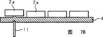
Fig. 7 A-7D is the figure of another example of the operation of the expression manufacture method that relates to semiconductor device of the present invention.Because the operation of Fig. 5 A-5C of the operation of Fig. 7 A-7C and execution mode 3 is identical,, omit their explanation so give identical number to same section.
The adsorbent equipment 12 of absorption sheet glass 2a is moved on the case member 22 of taking in the semiconductor element 21 with light accepting part, carry out the contraposition of sheet glass 2a so that after sheet glass 2a coheres on case member 22 by gluing layer 23, remove the adsorption function of adsorbent equipment 12, cohere sheet glass 2a (Fig. 7 D).Like this, make respective rights and require semiconductor device 7, that on the case member 22 of taking in semiconductor element 21, cohere base sheet (sheet glass 2a in this example).
In addition, in execution mode 3~5, about being illustrated under the situation of using the sheet glass 2a that abides by execution mode 1 manufacturing, but need not many speeches, under the situation of using the sheet glass 2a that interdicts film 6 with infrared ray that abides by execution mode 2 manufacturings, also can make semiconductor wafer or semiconductor device equally.In execution mode 3~5, under the situation of using the sheet glass 2a that interdicts film 6 with infrared ray that abides by execution mode 2 manufacturings, the illustrated second adhesion thin slice 4 among Fig. 5-7 is replaced into the 3rd adhesion thin slice 7, top configuration infrared ray blocking film 6 among the figure of illustrated sheet glass 2a in Fig. 5-7.In this case, because can nonreversible sheet glass 2a, configuration plane at the distant place configuration infrared ray blocking film 6 that leaves semiconductor wafer 14, if so be used in solid-state image pickup device, even on infrared ray blocking film 6, sneak into or adhere to dust, also can easily lower the bad generation that causes thus.
In addition, in above-mentioned example, use glass, but beyond glass, also can use the semiconductor substrate of silicon substrate etc., can be suitable for the present invention equally as matrix.As the example of the semiconductor wafer that is applicable to the semiconductor substrate that uses silicon substrate etc., can enumerate on the silicon wafer that forms function element, cohere the silicon chip that protective cover is used.As the example of the semiconductor device that is applicable to the semiconductor substrate that uses silicon substrate etc., can enumerate the device that cuts off the silicon wafer that coheres the silicon chip that its protective cover uses.
Claims (5)
1. the manufacture method of a semiconductor wafer is characterized in that, comprises the steps: to provide the glass basis that sticks on the first adhesion thin slice, and above-mentioned glass basis is cut into a plurality of glass basis sheets; Reduce the adhesion strength of the above-mentioned first adhesion thin slice by rayed; With the face of the above-mentioned glass basis sheet that is secured at the face opposition side of above-mentioned first adhesion on the thin slice on paste the second adhesion thin slice; Peel off the above-mentioned first adhesion thin slice from above-mentioned glass basis sheet, to remove attached to the glass basis smear metal on the above-mentioned first adhesion thin slice; By the cleaning of jet or washing lotion, remove attached to the glass basis smear metal on the above-mentioned glass basis sheet; Reduce the adhesion strength of the above-mentioned second adhesion thin slice by rayed; Peel off above-mentioned glass basis sheet after adhesion coating sticks on the semiconductor wafer from the above-mentioned second adhesion thin slice, above-mentioned semiconductor wafer has function element.
2. the manufacture method of semiconductor wafer as claimed in claim 1 is characterized in that, function element is a light receiving part.
3. the manufacture method of a semiconductor device is characterized in that, comprises the steps: to provide the glass basis that sticks on the first adhesion thin slice, and above-mentioned glass basis is cut into a plurality of glass basis sheets; Reduce the adhesion strength of the above-mentioned first adhesion thin slice by rayed; With the face of the above-mentioned glass basis sheet that is secured at the face opposition side of above-mentioned first adhesion on the thin slice on paste the second adhesion thin slice; Peel off the above-mentioned first adhesion thin slice from above-mentioned glass basis sheet, to remove attached to the glass basis smear metal on the above-mentioned first adhesion thin slice; By the cleaning of jet or washing lotion, remove attached to the glass basis smear metal on the above-mentioned glass basis sheet; Reduce the adhesion strength of the above-mentioned second adhesion thin slice by rayed; Peel off above-mentioned glass basis sheet after adhesion coating sticks on the semiconductor wafer from the above-mentioned second adhesion thin slice, above-mentioned semiconductor wafer has function element; Above-mentioned semiconductor wafer is cut into slices.
4. the manufacture method of semiconductor device as claimed in claim 3 is characterized in that, function element is a light receiving part.
5. the manufacture method of a semiconductor device is characterized in that, comprises the steps: to provide the glass basis that sticks on the first adhesion thin slice, and above-mentioned glass basis is cut into a plurality of glass basis sheets; Reduce the adhesion strength of the above-mentioned first adhesion thin slice by rayed; With the face of the above-mentioned glass basis sheet that is secured at the face opposition side of above-mentioned first adhesion on the thin slice on paste the second adhesion thin slice; Peel off the above-mentioned first adhesion thin slice from above-mentioned glass basis sheet, to remove attached to the glass basis smear metal on the above-mentioned first adhesion thin slice; By the cleaning of jet or washing lotion, remove attached to the glass basis smear metal on the above-mentioned glass basis sheet; Reduce the adhesion strength of the above-mentioned second adhesion thin slice by rayed; Peel off the peristome that sticks on the case member of taking in semiconductor element behind the glass basis sheet from the above-mentioned second adhesion thin slice.
Applications Claiming Priority (2)
| Application Number | Priority Date | Filing Date | Title |
|---|---|---|---|
| JP2004174721A JP3830497B2 (en) | 2004-06-11 | 2004-06-11 | Semiconductor wafer manufacturing method and semiconductor device manufacturing method |
| JP174721/04 | 2004-06-11 |
Publications (2)
| Publication Number | Publication Date |
|---|---|
| CN1716533A CN1716533A (en) | 2006-01-04 |
| CN100501910C true CN100501910C (en) | 2009-06-17 |
Family
ID=35004301
Family Applications (1)
| Application Number | Title | Priority Date | Filing Date |
|---|---|---|---|
| CNB2005100896161A Expired - Fee Related CN100501910C (en) | 2004-06-11 | 2005-06-11 | Manufacturing method for a base piece made to adhere to an adhesive sheet, for a semiconductor wafer and for a semiconductor device |
Country Status (6)
| Country | Link |
|---|---|
| US (1) | US7438780B2 (en) |
| EP (1) | EP1605521A3 (en) |
| JP (1) | JP3830497B2 (en) |
| KR (2) | KR100714778B1 (en) |
| CN (1) | CN100501910C (en) |
| TW (1) | TWI274405B (en) |
Families Citing this family (2)
| Publication number | Priority date | Publication date | Assignee | Title |
|---|---|---|---|---|
| TWI549268B (en) * | 2013-02-27 | 2016-09-11 | 精材科技股份有限公司 | Wafer packaging method |
| CN107738135A (en) * | 2017-11-24 | 2018-02-27 | 深圳市精品诚电子科技有限公司 | The method of machining eyeglass chip removal |
Family Cites Families (20)
| Publication number | Priority date | Publication date | Assignee | Title |
|---|---|---|---|---|
| USH208H (en) * | 1984-02-17 | 1987-02-03 | At&T Bell Laboratories | Packaging microminiature devices |
| IT8921420V0 (en) | 1989-07-13 | 1989-07-13 | Telettra Spa | SYSTEM AND CIRCUIT FOR THE CALCULATION OF TWO-DIMENSIONAL DISCRETE TRANSFORMED. |
| JPH03151666A (en) | 1989-11-08 | 1991-06-27 | Nec Corp | Manufacture of solid image-pickup device |
| JPH0653586B2 (en) * | 1990-03-08 | 1994-07-20 | 株式会社巴川製紙所 | Method for processing cap glass for solid-state imaging device |
| JP3165192B2 (en) * | 1991-03-28 | 2001-05-14 | 株式会社東芝 | Method for manufacturing semiconductor integrated circuit device |
| JPH0541461A (en) | 1991-08-02 | 1993-02-19 | Nippon Electric Glass Co Ltd | Manufacture of small glass panel with adhesive |
| US5591290A (en) * | 1995-01-23 | 1997-01-07 | Wallace Computer Services, Inc. | Method of making a laminate having variable adhesive properties |
| FR2764111A1 (en) * | 1997-06-03 | 1998-12-04 | Sgs Thomson Microelectronics | METHOD FOR MANUFACTURING SEMICONDUCTOR PACKAGES INCLUDING AN INTEGRATED CIRCUIT |
| JPH1140520A (en) * | 1997-07-23 | 1999-02-12 | Toshiba Corp | Method of dividing wafer and manufacture of semiconductor device |
| US6428650B1 (en) * | 1998-06-23 | 2002-08-06 | Amerasia International Technology, Inc. | Cover for an optical device and method for making same |
| JP3447602B2 (en) * | 1999-02-05 | 2003-09-16 | シャープ株式会社 | Method for manufacturing semiconductor device |
| JP3455762B2 (en) | 1999-11-11 | 2003-10-14 | カシオ計算機株式会社 | Semiconductor device and manufacturing method thereof |
| JP3906962B2 (en) * | 2000-08-31 | 2007-04-18 | リンテック株式会社 | Manufacturing method of semiconductor device |
| JP2003086540A (en) | 2001-09-07 | 2003-03-20 | Toshiba Corp | Manufacturing method of semiconductor device and manufacturing device thereof |
| JP3881888B2 (en) | 2001-12-27 | 2007-02-14 | セイコーエプソン株式会社 | Optical device manufacturing method |
| JP2003224085A (en) | 2002-01-30 | 2003-08-08 | Disco Abrasive Syst Ltd | Pickup method of semiconductor chip |
| JP2004040050A (en) | 2002-07-08 | 2004-02-05 | Toshiba Corp | Semiconductor-device manufacturing method and apparatus |
| JP2004296453A (en) | 2003-02-06 | 2004-10-21 | Sharp Corp | Solid-state imaging device, semiconductor wafer, optical device module, method of manufacturing the solid-state imaging device, and method of manufacturing the optical device module |
| JP4204368B2 (en) | 2003-03-28 | 2009-01-07 | シャープ株式会社 | Optical device module and method of manufacturing optical device module |
| JP4236594B2 (en) | 2004-01-27 | 2009-03-11 | シャープ株式会社 | Optical device module and method of manufacturing optical device module |
-
2004
- 2004-06-11 JP JP2004174721A patent/JP3830497B2/en not_active Expired - Fee Related
-
2005
- 2005-06-09 TW TW094119080A patent/TWI274405B/en not_active IP Right Cessation
- 2005-06-09 US US11/149,520 patent/US7438780B2/en active Active
- 2005-06-09 KR KR1020050049158A patent/KR100714778B1/en not_active IP Right Cessation
- 2005-06-10 EP EP05253596A patent/EP1605521A3/en not_active Withdrawn
- 2005-06-11 CN CNB2005100896161A patent/CN100501910C/en not_active Expired - Fee Related
-
2006
- 2006-11-24 KR KR1020060117211A patent/KR100768870B1/en not_active IP Right Cessation
Also Published As
| Publication number | Publication date |
|---|---|
| JP2005353921A (en) | 2005-12-22 |
| EP1605521A2 (en) | 2005-12-14 |
| EP1605521A3 (en) | 2007-08-08 |
| TW200601504A (en) | 2006-01-01 |
| KR20060132768A (en) | 2006-12-22 |
| TWI274405B (en) | 2007-02-21 |
| KR100768870B1 (en) | 2007-10-19 |
| CN1716533A (en) | 2006-01-04 |
| KR100714778B1 (en) | 2007-05-04 |
| KR20060048298A (en) | 2006-05-18 |
| US7438780B2 (en) | 2008-10-21 |
| US20050274451A1 (en) | 2005-12-15 |
| JP3830497B2 (en) | 2006-10-04 |
Similar Documents
| Publication | Publication Date | Title |
|---|---|---|
| JP5091066B2 (en) | Method for manufacturing solid-state imaging device | |
| CN1054437C (en) | Wafer-like processing after sawing dmds | |
| CN102468233B (en) | Method for manufacturing semiconductor wafer by laser cutting | |
| JP2020518133A5 (en) | ||
| KR101317983B1 (en) | Method for cutting solid-state image pickup device | |
| EP1372192B1 (en) | Method of manufacturing micro-semiconductor element | |
| CN100501910C (en) | Manufacturing method for a base piece made to adhere to an adhesive sheet, for a semiconductor wafer and for a semiconductor device | |
| CN102117861A (en) | Method for manufacturing amorphous mercury cadmium telluride monolithic integrated focal plane detector | |
| JP2009081201A (en) | Method of manufacturing backside irradiation type imaging device | |
| CN111009541A (en) | Packaging method for improving image effect and semiconductor device | |
| US9419050B2 (en) | Manufacturing method of semiconductor structure with protein tape | |
| CN102464296A (en) | Cutting separation method of MEMS structure | |
| TWI292186B (en) | Method of wafer level packaging and cutting | |
| JP5199217B2 (en) | Pellicle | |
| JPH05144938A (en) | Manufacture of solid-state image sensing device | |
| JP2006313921A (en) | Manufacturing method of substrate strip stuck on adhesive sheet | |
| TWI549268B (en) | Wafer packaging method | |
| KR101027844B1 (en) | Fabricating method for image sensor including wafer back grinding | |
| JP4328538B2 (en) | Manufacturing method of semiconductor device | |
| JPS6184062A (en) | Manufacture of detector assembly lighted from back | |
| TWI363405B (en) | Tools structure for chip redistribution and method of the same | |
| JP2005322695A (en) | Imaging device, its manufacturing process and camera module | |
| TWI226663B (en) | Glass substrate and precision finishing method thereof | |
| JP2013247175A (en) | Semiconductor device manufacturing method and semiconductor device | |
| JPH0653586B2 (en) | Method for processing cap glass for solid-state imaging device |
Legal Events
| Date | Code | Title | Description |
|---|---|---|---|
| C06 | Publication | ||
| PB01 | Publication | ||
| C10 | Entry into substantive examination | ||
| SE01 | Entry into force of request for substantive examination | ||
| C14 | Grant of patent or utility model | ||
| GR01 | Patent grant | ||
| CF01 | Termination of patent right due to non-payment of annual fee |
Granted publication date: 20090617 Termination date: 20160611 |
|
| CF01 | Termination of patent right due to non-payment of annual fee |