CN100565942C - Be used for optoelectronic semiconductor chip and manufacture method thereof - Google Patents
Be used for optoelectronic semiconductor chip and manufacture method thereof Download PDFInfo
- Publication number
- CN100565942C CN100565942C CNB018170358A CN01817035A CN100565942C CN 100565942 C CN100565942 C CN 100565942C CN B018170358 A CNB018170358 A CN B018170358A CN 01817035 A CN01817035 A CN 01817035A CN 100565942 C CN100565942 C CN 100565942C
- Authority
- CN
- China
- Prior art keywords
- semiconductor chip
- thin layer
- table top
- layer
- active area
- Prior art date
- Legal status (The legal status is an assumption and is not a legal conclusion. Google has not performed a legal analysis and makes no representation as to the accuracy of the status listed.)
- Expired - Lifetime
Links
Images


Classifications
-
- H—ELECTRICITY
- H01—ELECTRIC ELEMENTS
- H01L—SEMICONDUCTOR DEVICES NOT COVERED BY CLASS H10
- H01L33/00—Semiconductor devices with at least one potential-jump barrier or surface barrier specially adapted for light emission; Processes or apparatus specially adapted for the manufacture or treatment thereof or of parts thereof; Details thereof
- H01L33/02—Semiconductor devices with at least one potential-jump barrier or surface barrier specially adapted for light emission; Processes or apparatus specially adapted for the manufacture or treatment thereof or of parts thereof; Details thereof characterised by the semiconductor bodies
- H01L33/20—Semiconductor devices with at least one potential-jump barrier or surface barrier specially adapted for light emission; Processes or apparatus specially adapted for the manufacture or treatment thereof or of parts thereof; Details thereof characterised by the semiconductor bodies with a particular shape, e.g. curved or truncated substrate
-
- H—ELECTRICITY
- H01—ELECTRIC ELEMENTS
- H01L—SEMICONDUCTOR DEVICES NOT COVERED BY CLASS H10
- H01L33/00—Semiconductor devices with at least one potential-jump barrier or surface barrier specially adapted for light emission; Processes or apparatus specially adapted for the manufacture or treatment thereof or of parts thereof; Details thereof
- H01L33/005—Processes
- H01L33/0093—Wafer bonding; Removal of the growth substrate
-
- H—ELECTRICITY
- H01—ELECTRIC ELEMENTS
- H01L—SEMICONDUCTOR DEVICES NOT COVERED BY CLASS H10
- H01L33/00—Semiconductor devices with at least one potential-jump barrier or surface barrier specially adapted for light emission; Processes or apparatus specially adapted for the manufacture or treatment thereof or of parts thereof; Details thereof
- H01L33/02—Semiconductor devices with at least one potential-jump barrier or surface barrier specially adapted for light emission; Processes or apparatus specially adapted for the manufacture or treatment thereof or of parts thereof; Details thereof characterised by the semiconductor bodies
- H01L33/08—Semiconductor devices with at least one potential-jump barrier or surface barrier specially adapted for light emission; Processes or apparatus specially adapted for the manufacture or treatment thereof or of parts thereof; Details thereof characterised by the semiconductor bodies with a plurality of light emitting regions, e.g. laterally discontinuous light emitting layer or photoluminescent region integrated within the semiconductor body
-
- H—ELECTRICITY
- H01—ELECTRIC ELEMENTS
- H01L—SEMICONDUCTOR DEVICES NOT COVERED BY CLASS H10
- H01L33/00—Semiconductor devices with at least one potential-jump barrier or surface barrier specially adapted for light emission; Processes or apparatus specially adapted for the manufacture or treatment thereof or of parts thereof; Details thereof
- H01L33/02—Semiconductor devices with at least one potential-jump barrier or surface barrier specially adapted for light emission; Processes or apparatus specially adapted for the manufacture or treatment thereof or of parts thereof; Details thereof characterised by the semiconductor bodies
- H01L33/10—Semiconductor devices with at least one potential-jump barrier or surface barrier specially adapted for light emission; Processes or apparatus specially adapted for the manufacture or treatment thereof or of parts thereof; Details thereof characterised by the semiconductor bodies with a light reflecting structure, e.g. semiconductor Bragg reflector
-
- H—ELECTRICITY
- H01—ELECTRIC ELEMENTS
- H01L—SEMICONDUCTOR DEVICES NOT COVERED BY CLASS H10
- H01L2924/00—Indexing scheme for arrangements or methods for connecting or disconnecting semiconductor or solid-state bodies as covered by H01L24/00
- H01L2924/0001—Technical content checked by a classifier
- H01L2924/0002—Not covered by any one of groups H01L24/00, H01L24/00 and H01L2224/00
-
- H—ELECTRICITY
- H01—ELECTRIC ELEMENTS
- H01L—SEMICONDUCTOR DEVICES NOT COVERED BY CLASS H10
- H01L33/00—Semiconductor devices with at least one potential-jump barrier or surface barrier specially adapted for light emission; Processes or apparatus specially adapted for the manufacture or treatment thereof or of parts thereof; Details thereof
- H01L33/02—Semiconductor devices with at least one potential-jump barrier or surface barrier specially adapted for light emission; Processes or apparatus specially adapted for the manufacture or treatment thereof or of parts thereof; Details thereof characterised by the semiconductor bodies
- H01L33/26—Materials of the light emitting region
- H01L33/30—Materials of the light emitting region containing only elements of group III and group V of the periodic system
-
- H—ELECTRICITY
- H01—ELECTRIC ELEMENTS
- H01L—SEMICONDUCTOR DEVICES NOT COVERED BY CLASS H10
- H01L33/00—Semiconductor devices with at least one potential-jump barrier or surface barrier specially adapted for light emission; Processes or apparatus specially adapted for the manufacture or treatment thereof or of parts thereof; Details thereof
- H01L33/36—Semiconductor devices with at least one potential-jump barrier or surface barrier specially adapted for light emission; Processes or apparatus specially adapted for the manufacture or treatment thereof or of parts thereof; Details thereof characterised by the electrodes
- H01L33/40—Materials therefor
- H01L33/405—Reflective materials
Abstract
Semiconductor chip, especially radiation-emitting semiconductor chip, it has an active thin layer (2) and a carrier substrates (1) that is used for thin layer (2), form the zone (3) of a ballistic phonon in this thin layer, this substrate is arranged on being connected of thin layer (2) on that side of chip radiation direction and with this thin layer.In active thin layer (2), form at least one hole (8) from carrier substrates (1), by this hole, the boundary between carrier substrates (1) and thin layer (2) forms many table tops (4).
Description
Technical field
The present invention relates to be used for optoelectronic semiconductor chip, relate in particular to radiation-emitting semiconductor chip, it has:
-one active thin layer and especially based on In
1-x-yAl
xGa
yThe thin layer of P (wherein 0≤x≤1,0≤y≤1, x+y≤1) forms the zone of a ballistic phonon in this thin layer,
-one carrier substrates that is used for thin layer, it is arranged on being connected of this thin layer on that side of chip transmit direction and with this thin layer.
The invention still further relates to the method for making many such semiconductor chips simultaneously.
Background technology
Substrate itself is the part of semiconductor chip and is that the mechanical support layer of thin layer is the main supporting member of thin layer that this no longer includes thin layer from supporting course on that side relative with substrate.
Based on In
1-x-yAl
xGa
yThe thin layer of P (wherein 0≤x≤1,0≤y≤1, x+y≤1) means that thin layer has many layers, and they are by mixing up or unadulterated In
1-x-yAl
xGa
yP (wherein 0≤x≤1,0≤y≤1, x+y≤1) based material is made.
US5008718 and US5367580 disclose the semiconductor chip of the above-mentioned type.In order to make the semiconductor chip of the above-mentioned type, be coated with on a substrate by epitaxy method usually and apply an active semi-conductor sequence of layer.Then, on the surface of this active semi-conductor sequence of layer, fixing a carrier substrates.At least a portion that the substrate of this semiconductor layer sequence in deposit on it is removed.Being preferably between this carrier substrates and this active semi-conductor sequence of layer has a metallic reflector, makes not absorbing light of carrier substrates.
A shortcoming of this known semiconductor chip is that the metallic reflector that is arranged between carrier substrates and the active semi-conductor sequence of layer does not generally have gratifying reflectivity in short-term at wavelength.Especially when wavelength is shorter than 600 nanometers, more and more lower as the efficient of the gold of metallic reflector, because reflectivity obviously reduces.When wavelength is shorter than 600 nanometers, for example can adopt element al and Ag, their reflectivity is shorter than at wavelength and keeps more stable under the situation of 600 nanometers.
In addition, engage large tracts of land reflector such as metallic reflector and brought difficulty.In addition, because also there are sizable danger of the quality of infringement metallic reflector in the joint and the alloying of metal contact layer.
In addition, DE19807758A1 discloses a kind of section pyramid semiconductor chip, and it has an active luminous zone between Window layer on and a following Window layer.Should go up Window layer and constitute this section pyramid matrix together with this time Window layer.The tilted alignment of Window layer sidewall make light from active area on the side total reflection and almost vertically directive cut the bottom surface of playing the light-emitting area effect of pyramid shaped body.So, the part of the light that sends from active area goes out the pencil injection to the surface at semiconductor element.
Here, go out that pencil is meant and followingly should be meant such cone, be that it is made of light, the incidence angle that described light incides exit facet is less than the cirtical angle of total reflection and these light thereby not by total reflection, but directly is coupled output from semi-conducting material.Therefore, the angular aperture that goes out pencil is the twice of the cirtical angle of total reflection.Those hit the light of exit facet by total reflection with an angle bigger than the cirtical angle of total reflection in other words what go out that the pencil extension stretches.
In order to enlarge markedly light output, the prerequisite of this conception is exactly that upper and lower window has minimum thickness.Known cutting in the pyramid semiconductor element, the thickness of upper and lower Window layer is at least 50.8 microns (2millizoll).Such bed thickness is still in the scope that can accomplish.But,, then must demarcate whole dimension if improve the power of known semiconductor chip.Under these circumstances, obtained the bed thickness that can only form by extensional mode soon very bothersomely.So this known semiconductor chip can only technically be demarcated usually very bothersomely.
Summary of the invention
Based on such prior art, task of the present invention provide a kind of can according to the thin film technique manufacturing and have the semiconductor chip and a manufacture method thereof of better optical coupling output.
According to the present invention, finish above-mentioned task by semiconductor chip as described below and method.Preferred form of implementation and manufacturing method for semiconductor chips see below simultaneously.
According to a first aspect of the invention, a kind of radiation-emitting semiconductor chip is provided, it has a thin layer, in this thin layer, form the active area of a ballistic phonon, described thin layer is being provided with at least one hole on a side of the transmit direction of semiconductor chip, a plurality of table tops have been formed by described hole, make described thin layer comprise the coating of described a plurality of table top and and described table top adjacency, the degree of depth of wherein said hole is configured to make hole not disconnect described active area, thereby described active area is formed in the described coating.
According to a second aspect of the invention, provide a kind of be used for making simultaneously a plurality ofly be used for optoelectronic and the method for the semiconductor chip of a thin layer arranged, form the active area of a ballistic phonon in this thin layer, this method may further comprise the steps: make a sequence of layer epitaxial growth that has comprised the active area of described ballistic phonon on a growth substrates; In this sequence of layer, form at least one hole, make and in this sequence of layer, form a plurality of table tops, thereby make described thin layer comprise the coating of described a plurality of table top and and described table top adjacency, wherein, described hole is constructed with small depth and causes the active area of described ballistic phonon not to be disconnected, and is formed in the described coating; To be installed to by the complex that growth substrates and sequence of layer constitute on the carrier substrates, and make table top face carrier substrates, and this complex is connected with carrier substrates; An electric contact connection portion is arranged on that face relative of this sequence of layer with table top; To be divided into semiconductor chip by the complex that carrier substrates and structurized sequence of layer are constituted along separated track.
In a particularly preferred form of implementation of semiconductor chip, the hole cross section dwindles from outside to inside, in other words, internally dwindles to thin layer from the interface with carrier substrates, and the degree of depth of hole is greater than thin layer one half thickness.
Hole or advantageously cause thin layer to have seal face on the one hand on it is connected to connection side on the carrier substrates by the many table tops that hole forms, this seal face is compared very little with the entire cross section of chip.This has brought following advantage, promptly in the seal face zone that dwindles, can produce bigger local pressure, this pressure has promoted substrate and the reliable of thin layer to be connected, but simultaneously, can keep enough for a short time to exerting pressure of thin layer, so that eliminate thin layer impaired danger when being connected as much as possible with carrier substrates.
On the other hand, operational joint face increases because of hole is arranged, and this also can cause the improvement that is connected between carrier substrates and the thin layer.In addition, hole is used to hold unnecessary adhesive or scolder, and this advantageously makes it quantitatively become not too important.
In addition, advantageously provided such side by hole, promptly on these sides, part is diverted from the radiation of active area, thereby the exit facet back to carrier substrates of active thin layer is hit in this part radiation in going out pencil.Compared with prior art, in semiconductor chip of the present invention, replaced reflection on a continuous plane reflection layer in the small part that reflexes on the side of table top.
Here advantageously, the side charge into as far as possible in the thin layer in case make as much as possible from active area and radiation that directly do not hit exit facet and coupling output there so (even repeatedly) reflection promptly turn to, i.e. this part radiation is hit exit facet with an angle in going out pencil.
Experiment shows that when the half of the hole degree of depth greater than thin layer thickness, the coupling delivery efficiency obviously improves.
In a form of implementation of the present invention, the degree of depth of hole can make the active area of active thin layer be divided disconnection by hole.
Fact proved that its active area is had extra high light output by a hole that is opened in the active thin layer from fixation side by minute semiconductor chip of disconnection.Because in this case, be not only the photon of directive fixation side, and the photon of the active thin layer exit facet of at least a portion directive turns to exit facet by the reflection on the side of table top with an angle that is positioned at pencil.
Cause most of photon going out to hit exit facet in the pencil and can leave semiconductor chip in the reflection on the table top interface from active area.
In another preferred implementing form, thin layer is so to constitute, and promptly at least one track of the photon that sends from active area leads to one of them adjacent table top from that time table top.
By making the table top optical coupled, the photon that does not reflect on one of them side of former table top enters in one of them adjacent table top and is so reflected on the side of at that time table top there, and promptly this part photon hits exit facet in going out pencil.
In addition, in a favourable execution mode of the present invention, table top is equipped with concave side.
By these measures, the trend of radiation is such, and promptly they at first continue reflection on the side at a table top in reflection on the exit facet and each subsequently exit facet relatively steeplyer, thereby exit facet is finally hit in these radiation in going out pencil.
In another preferred implementing form, these table tops are covered by a reflector.
By this measure, the light radiation of all hitting the table top side is diverted the exiting side of semiconductor chip.
In a preferred implementing form, thin layer has 5-50 micron, the especially thickness of 5-25 micron.
Description of drawings
From the embodiment that describes below in conjunction with accompanying drawing, obtained other advantageous forms of implementation semiconductor chip of the present invention and the inventive method, wherein:
Fig. 1 is the cross sectional representation of semiconductor chip of the present invention;
Fig. 2 is the cross sectional representation of another embodiment of semiconductor chip of the present invention, and wherein active area is separately positioned on and cuts in the pyramid table top;
Fig. 3 is the cross sectional representation of semiconductor chip of the present invention, and this semiconductor chip is equipped with the table top with concave side;
Fig. 4 is a curve chart, and it shows the light of semiconductor chip of the present invention and exports the situation of comparing rising with the conventional semiconductors chip;
Fig. 5 is the cross sectional representation of a table top, and this table top is made of the flat truncated cone of a below and the steep truncated cone of a top;
Fig. 6 a-6d is the schematic diagram and a curve chart of the varying cross-section shape of table top, and this curve chart shows following section pyramid of coupling delivery efficiency and table top shown in Figure 5 and goes up the relation of the radius that cuts the interface between the pyramid;
Fig. 7 is a curve chart, its expression coupling delivery efficiency and the relation that is arranged on the reflectivity of the contact layer on the table top tip shown in Figure 5;
Fig. 8 is a curve chart, and it shows the relation of reflectivity of the side of coupling delivery efficiency and table top shown in Figure 5;
Fig. 9 is a curve chart, the relation of the delivery efficiency that therefrom is coupled as can be seen and the spot size in active area;
Figure 10 a-10d is the schematic diagram and a curve chart of the varying cross-section shape of a table top, and in table top, the active area height changes, and this curve chart shows the relation of the thickness of a coupling delivery efficiency and a following boundary layer;
Figure 11 is a curve chart, and it shows coupling delivery efficiency and the relation with angle of flange of the side of the table top of shape of cross section shown in Figure 10 b;
Figure 12 is another curve chart, and it shows coupling delivery efficiency and the relation with angle of flange of the table top of shape of cross section shown in Figure 10 b;
Figure 13 is a curve chart, and it shows the coupling delivery efficiency when thickness remains unchanged and the relation of active thin layer width;
Figure 14 is a curve chart, and it shows the relation that is connected the table top coating layer ranges in thickness of coupling delivery efficiency and the table top that is used for various mesa shape;
Figure 15 is the cross sectional representation of another embodiment of semiconductor chip of the present invention;
Figure 16 is the cross sectional representation of another embodiment of semiconductor chip of the present invention;
Figure 17 a-17e is the schematic diagram of process that is used to make first method of a plurality of semiconductor chips of the present invention;
Figure 18 a-18e is the schematic diagram of process that is used to make second method of a plurality of semiconductor chips of the present invention;
Figure 19 a-19e is the schematic diagram of process that is used to make third party's method of a plurality of semiconductor chips of the present invention;
Figure 20 is the vertical view of semiconductor chip of the present invention;
Figure 21 is the oblique view on the thin layer surface after forming hole;
Figure 22 is the partial enlarged drawing of Figure 21.
Embodiment
In these figure, identical or act on identical embodiment part and represent with identical Reference numeral.
The semiconductor chip that is used for light-emitting diode shown in Figure 1 has a carrier substrates 1, is coated with active thin layer 2 on this carrier substrates.For clarity sake, in Fig. 1, compare the thickness that shows active thin layer 2 large with substrate 1 thickness.Active thin layer 2 has the active area 3 of a ballistic phonon, and this active area always is formed on intermediate altitude in the table top 4.Table top 4 can become to cut pyramid or truncated cone shape.Therefore, semiconductor chip is exactly a light-emitting diode.
Insulating barrier 9 preferably has a refractive index littler than the adjacent semiconductor layer of thin layer 2.This insulating barrier also is configured for the barrier layer of metal layer 10.Replace insulating barrier 9, also can use a conductive layer.The optical property of this layer is conclusive.
In order to make semiconductor chip as shown in Figure 1, at first, the active thin layer 2 of epitaxial growth on a growth substrates.Active thin layer 2 for example can based on InGaAlP make, wherein, coating 5 at first is formed on the growth substrates, subsequently, to be higher than 10
18Cm
-3Above concentration is mixed up, and to guarantee the satisfactory electrical conductivity of coating 5, this is that promptly on the front 6 of light-emitting diode chip for backlight unit, contact site, a center 7 is enough to the active area supply of current to many table tops 4 because the satisfactory electrical conductivity of coating 5 is following preconditions.In addition, the composition of coating 5 is so to select, and promptly it is transparent to the photon that produces in active area.Usually, this can regulate the gap, forbidden band by the material composition that utilizes coating 5 and realizes.
Subsequently, be coated with on coating 5 and be covered with another layer, in this layer, form table top 4 by suitable chemical wet or chemical dry etching, these engraving methods are not the application's contents.Table top 4 preferably only is formed in the zone of establishing for semiconductor chip and is preferably in the there again only in the zone that optical coupling output can take place, rather than below thin layer 2 lip- deep contact layers 7,43,49.These zones of establishing for semiconductor chip have 400 microns square typical transverse outside dimensions.Table top 4 has such outside dimension, and promptly this outside dimension is in the bed thickness scope of active thin layer 2.Therefore, the outside dimension of table top 4 is in 10 micrometer ranges.
In another step, deposition insulating layer 9 and formation contacting portion 12 on table top 4.Subsequently, be coated with and be covered with metal layer 10.
Subsequently, active thin layer 2 number of chips according to the rules is separated.This for example realizes by Wet-type etching.
Then, the active thin layer 2 that separates for example engages to be fixed on the substrate 1 and by Wet-type etching by eutectic removes growth substrates.Then, formation contact site 7 and semiconductor chip are separated by carrier of separating substrate 1 on the open front of active thin layer 2.
Semiconductor chip shown in Figure 1 has the following advantages, and promptly the photon that is produced by active area 3 is not mapped on the semiconductor chip composition that absorbs photon, because make photon away from carrier substrates 1 by metal layer 10.Therefore, substrate is advantageously well being optimized aspect conduction and/or heat-transfer capability and/or the thermal expansion.
Another advantage is, in the semiconductor chip of Fig. 1, and overwhelming majority emission entirely on the side 13 of table top 4 of the photon that sends by active area 3.The photon of total reflection is with a big angle directive front 6 on side 13.Especially, not on side 13 reflection and a part of photon of going up full emission in front going out the pencil injection to front 6 and thereby can leave semiconductor chip.So, in the semiconductor chip of Fig. 1, replaced disclosed reflection on continuous bottom surface from prior art by the total reflection on side 13 at least in part.Therefore, the semiconductor chip of Fig. 1 is compared with the conventional semiconductors chip that does not have hole 8 and is had the light output that has almost increased twice.
Below, describe above-mentioned effect in detail in conjunction with other embodiment shown in Fig. 2,3.
Note a row light radiation, wherein term " light radiation " is not meant and is confined to certain wavelength, and is meant the method for geometrical optics that is confined to Wavelength-independent.
In the embodiment shown in Figure 2,4 one-tenth of table tops cut Pyramids and it only is fixed on the carrier substrates 1 by a contact layer 14 on table top 4 bottom surfaces 11.By contact layer 4, give active area 3 supply of current.
Because the refringence between semiconductor and the casting resin is generally up to 3.5: 1.5, so on the interface between semiconductor and the casting resin, can only be coupled from semiconductor and export light radiation, described light radiation goes out in the pencil at one injects the interface with about 16 ° angular aperture.Divide equally when injecting in the light radiation equal angles, this approximates 2% of light radiation that unit are injects.
By table top 4, turn to front 6 from the light radiation of active area 3.The effect of table top 4 is to make the light radiation of directive side 13 turn to front 6 and hit in going out pencil there, thereby described light radiation can be left semiconductor chip.In addition, light output can be optimized by size, side 13 inclination angle sizes and table top 4 height and active area 3 positions of suitable selection bottom surface 11.
A light radiation 15 shown in Figure 2, its at first total reflection and turn to front 6 therefrom on side 13.In front on 6, light radiation is going out the pencil injection to the interface and thereby can leave semiconductor chip.Not under the situation of total reflection on the side 13, light radiation 15 can be in front total reflection and retroeflection are to a disclosed reflector from prior art on 6, here, light radiation can be reflected again.In the embodiment shown in Figure 2, the reflection on traditional continuous reflection layer has been replaced by the reflection on side 13.
This also is applicable to light radiation 16, and it is at first reflecting on side 13 on the bottom surface 11 and then.Light radiation 16 is also turning to front 6 after the reflection for the second time, and there, this light radiation is hit in outgoing.Not under the situation of reflection on the side 13, light radiation 16 also can be in front on 6 total reflection and retroeflection to a backside reflection layer.
Also advantageously, table top 4 passes through coating 5 by optical coupled.Here, optical coupled is meant that at least one light radiation from thin layer 2 can surpass center line 17 ground arrive an adjacent table top 4 from the zone of one of them table top 4 zone.Hit one of them side 13 of one of them adjacent table top 4 and turn to front 6 there because carry out the light radiation 18 that optical coupled can make a side 13 that does not have directive table top 4 at that time by coating 5, here, light radiation goes out in the pencil to hit at one.So,, further increased light output by optical coupled by coating 5.
At last, figure 3 illustrates the cross section of a variant embodiment of semiconductor chip, wherein 4 one-tenth truncated cone shapes of table top with concave side 13.This side 13 project organizations have caused, one in front 6 and side 13 between come the light radiation 18 of back reflective near center line 17 time, to turn to the front gradually, going out to hit front 6 in the pencil up to it.This also is applicable to light radiation 19, and described light radiation 19 at first arrives adjacent table top 4 and arrives front 6 with a wide-angle there from separately table top 4 by coating 5.
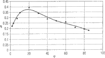
At last, figure 4 illustrates a curve chart, in this curve chart, one measure curve 20 expressions according to the light output of units concerned when the traditional light-emitting diode pulsed operation of making according to thin film technique and the correlation of operating current.Another measures curve 21 expressions according to the light output of units concerned and correlation according to the operating current of light-emitting diode embodiment illustrated in fig. 3.Can see from Fig. 4 that light output in the embodiment shown in fig. 3 approximately is the twice that does not have the output of the light of the conventional semiconductors chip of hole 8.
In order to determine the optimum shape of table top 4, a series of experiments have been carried out.Below, describe experimental result in detail in conjunction with Fig. 5-Figure 14.
At first, in conjunction with Fig. 5 the parameter that changes is described in experiment.In Fig. 5, show the shape of cross section of one of them table top 4.In the illustrated case, table top 4 is made of a following truncated cone 22 and a last truncated cone 23.Following truncated cone 22 is adjacent with coating 5 with a basal plane 24.In last truncated cone 23, form this active area 3.In addition, in Fig. 5, be provided with a contact site 25 on the bottom surface 11 that is arranged at table top 3.
The side 13 of table top 4 is made of a flange 26 of following truncated cone 22 and a flange 27 of last truncated cone 23.Physical dimension along the following truncated cone 22 at common interface 28 is so to select, and promptly flange 26 transits directly in the flange 27.
Each size that below relates to table top 4.The radius r of following truncated cone 22 basal planes 24
nExpression, the radius r at interface 28
tExpression, bottom surface 11 radius r
pExpression.In addition, table top 4 can be divided into one in the following boundary layer 29 between basal plane 24 and the active area 3 and one boundary layer 30 between active area 3 and the bottom surface 11.Here, following boundary layer 29 has thickness h
u, last boundary layer has thickness h
0The gross thickness of also representing table top with H.In all experiments, gross thickness all is set to 6 microns.Thickness h as for coating 5
w, in its all thickness h
wIn all constant experiment, it is set to 2 microns.
In Fig. 6 a-6d result of calculation has been shown, wherein the radius of bottom surface 11 is by r
pBe set to 5 microns, the radius r of basal plane 24
nBe set to 20 microns.In the shape of cross section shown in Fig. 6 a-6d, the radius r at interface 28
tBetween 6 microns-18 microns, change.
In these experiments, 3.2 refractive indexes are used to active area 3.The refractive index of following boundary layer 29, the refractive index that goes up boundary layer 30 and the refractive index of coating 5 all are 3.3.Under immovable situation, adopted to equal 0.3 contact site 25 reflectivity.Be not touched the bottom surface 11 that position 25 covers and the reflectivity of flange 26,27 and be set to 0.8.Here, reflectivity is meant the reflection coefficient relevant with energy respectively.
In addition, considered the self-absorption of active area 3 by the absorption coefficient of 10.000/cm.All experiments are undertaken by the photon circulation.Suppose that for this reason internal quantum is 0.8.Do not consider the quantum efficiency when producing photon because of the charge carrier reorganization.Therefore, the coupling delivery efficiency η that indicates in curve chart equals the photon of coupling output from semiconductor chip and the ratio of the actual photon amount that produces.Therefore, the value of the coupling delivery efficiency η that indicates must multiply by coefficient 0.8, so that obtain external efficiencies.
Also supposition, reflection on contact site 25 and flange 26,27 and angle are irrelevant.So, occur such situation in experiment, promptly at first dielectric insulation layer 9 is applied to the metal layer 10 that also replenishes mirror image on the table top 4, has underestimated its effect in experiment, this is because do not consider the total reflection that occurs in the case in experiment.
Fig. 6 c represents a curve chart, wherein, and relative radius r
tGround shows coupling delivery efficiency η with a curve 31.For relatively, also show the coupling delivery efficiency of a general thin semiconductor chip, wherein only in the photon range of DO, measure scattering.The thin-film semiconductor chip that the edge is long 300 microns has and the same extension tissue of table top 4 in truncated cone 22 down and last truncated cone 23.Suppose that semiconductor chip has a minute surface in p type district, its reflectivity is 0.72.This value is the reflectivity mean value of the usefulness coverage rate weighting of reflector and contact layer, wherein, and for the reflectivity in reflector, this value is that the coverage rate in 0.8 reflector is 0.85, for the reflectivity of contact layer, this value is 0.3, and adopts 0.15 coverage rate.
Can from Fig. 6, see, under the situation that the angle of attack of truncated cone 23 is very big on according to the shape of cross section of Fig. 6 a, coupling delivery efficiency η may not be certain to be higher than traditional thin-film led coupling delivery efficiency η, shows its coupling delivery efficiency by straight line 32 in Fig. 6 d.This also is understandable, may not be certain just to make light radiation from active area 3 with acute angle directive light-emitting area 6 because have the table top 4 of face shape of cross section smooth shown in Fig. 6 a.And exactly, this can only realize by the table top 4 with shape of cross section shown in Fig. 6 c, and in this case, coupling delivery efficiency η also almost is the twice of traditional thin-film led coupling delivery efficiency η.
In addition, tested the relation that is coupled between delivery efficiency η and contact site 25 reflectivity.For this reason, according to the albedometer of the contact site 25 coupling delivery efficiency η that lets it pass, here, the shape of cross section of table top 4 equals the shape of cross section shown in Fig. 6 b.Supposition in addition, contact site 25 covers whole bottom surface 11.Can see from Fig. 7 that the reflectivity of coupling delivery efficiency η and contact site 25 does not have much relations.So, with traditional thin-film led comparing, it seems that the semiconductor chip of table top 4 described herein, as to have the fixation side of being located at contact site 25 wanted much insensitive than antiradar reflectivity, the repeatedly reflection of exporting obviously has only fraction to carry out between bottom surface 11 and light-emitting area 6 because cause being coupled, and is that solid is carried out in table top 4.
With the relative independence of contact site 25 reflectivity is particularly advantageous, and this is because in fact, the low ohmic resistance between contact site 25 and last boundary layer 30 is generally relevant with antiradar reflectivity.Because good Ohmic contact needs atom to be diffused into from the layer that constitutes contact site 25 in the material under it.
With with the relation of contact site 25 reflectivity on the contrary, coupling delivery efficiency η is very noticeable with the relation of the reflectivity Rs of minute surface on bottom surface 11 and flange 26,27.Such result of calculation shown, this calculating is that a model by semiconductor chip carries out, and the radius of the table top 4 of this semiconductor chip is r
n=20 microns, r
t=16 microns, r
p=5 microns.
So table top 4 roughly has the shape of cross section shown in Fig. 6 b.
This result of calculation is exactly a curve shown in Figure 8 33, and it raises with reflectivity Rs increase monotonously.Point 34 expressions of drawing in the curve chart of Fig. 8 are used for the result of calculation of such semiconductor chip, promptly on this semiconductor chip, never apply specular layer, but this semiconductor chip is imbedded as in the resin that surrounds material.But occurred total reflection here, thereby compared, produced a bigger coupling delivery efficiency with semiconductor chip with specular layer.In the embodiment shown in fig. 1, situation also is so, in this embodiment, is provided with electric insulation layer between metal layer 10, also can on this electric insulation layer total reflection take place.
Fig. 9 comprises such result calculated, i.e. this calculating is to carry out having on the semiconductor chip of table top, and its radius is r
n=20 microns, r
t=16 microns, r
p=5 microns.So this table top 4 roughly has the shape of cross section shown in Fig. 6 b.Here, active area 3 is on the intermediate altitude between basal plane 24 and the bottom surface 11.In this calculating, the zone that occurs photon in its active area 3 is restricted to a hot spot, this spot diameter d
LBe plotted on the abscissa.In conjunction with the curve chart of Fig. 9, can see that the coupling delivery efficiency is hour high especially at hot spot.This means that photon is coupled particularly well at the center of active area 3 and exports.Thus, there is more weak Wai Shi effect.
In addition, tested the influence of active area 3 positions.Various shape of cross sections have been shown in Figure 10 a-10c, have wherein so changed the thickness h of boundary layer 29 down
uThickness h with last boundary layer 30
0, promptly the gross thickness H of table top remains unchanged.Figure 10 d shows result of calculation, in the figure, and with the thickness h of following boundary layer 29
uDraw out coupling delivery efficiency η relevantly.As shown in the figure, the relation of coupling delivery efficiency η and active area 3 positions is little.A preferred active area 3 that is arranged in table top 4 Lower Halves, this is that this has been avoided problem of aging and linear problem because the current density of the active area 3 of flowing through is also low thereby the current capacity of active area 3 keeps low.
In addition, flange 27 angle of attack ψ have been tested
0With flange 26 angle of attack ψ
uInfluence.Based on such shape of cross section, wherein descend truncated cone 22 to have identical angle of attack ψ respectively here, with last truncated cone 23
0, ψ
uValue.Here, the radius ψ of active area 3
0Be always 10 microns, angle of attack ψ=ψ
0=ψ
uChange.Note two kinds of situations at this.On the one hand, experiment is used for the coupling delivery efficiency η of periodic boundary condition, and wherein the intercardinal distance is 10 microns.In the curve chart of Figure 11, in curve 35, determined the result.In addition, tested the aperiodicity situation.Calculate a coupling delivery efficiency η with semiconductor chip of an independent table top 4, here, all photon coatings 5 of injecting coating 5 absorb for this reason.In Figure 11, depicted the aperiodicity situation by curve 36.As shown in figure 11,5 pairs of couplings of coating delivery efficiency η has obvious contribution.
For angle of flange ψ, also there is a best region.This zone as shown in figure 12.In basic calculation, establish radius r
pEqual 10 microns.So change the radius r of active area 3
aRadius r with basal plane 24
n, promptly the angle of attack ψ of flange 27,26 covers 1.5 °-85 ° scope.As shown in figure 12, the angle of attack ψ angular range that has a best.Angle of flange ψ should be 5 °-60 ° and preferably 10 °-40 °.When angle of attack ψ is 15 °-30 °, obtain extraordinary coupling delivery efficiency η value.
Tested the width that changes table top 4 at last which type of influence coupling delivery efficiency η has been had.Therefore here, table top 4 thickness H remain unchanged radius r
p, r
a, r
nUniformity ground extends.At the such situation of curve 37 expressions of Figure 13, i.e. the reflectivity R of contact site 25
KEqual 0.3.Another curve 38 relates to the reflectivity R of contact site 25
KEqual 0.8 situation.Curve 37,38 is all represented coupling delivery efficiency η and active area 3 diameter 2r
aRelation.25 when having high reflectance in the contact site, and coupling delivery efficiency η only reduces slightly along with the increase of active area 3 diameters.But, the reflectivity R of expression contact site 25
KThe curve 37 of low actual conditions shows that coupling delivery efficiency η significantly reduces along with the increase of active area 3 diameters.So the horizontal expansion of table top 4 is more little, η is high more for the coupling delivery efficiency.
The thickness of coating 5 is also very important to coupling delivery efficiency η.In Figure 14, with coating 5 thickness h
wShow the coupling delivery efficiency η that is used for various situations relevantly.The above-mentioned periodicity situation of curve 39 explanations.Another curve 40 relates to the aperiodicity situation, and the 3rd curve 41 relates to 300 square square semiconductor chips and passes through the interconnective situation of articulamentum.Can see from Figure 14 that the coating 5 that bed thickness increases is favourable all the more.Especially, if bed thickness h
wLess than table top 4 thickness that are 6 microns here, then this is very favourable.As a result, the degree of depth of hole 8 should be greater than half of active thin layer 2 thickness.
But, as shown in figure 14, there are many independently semiconductor chips of a table top 4 to show optimal cases respectively, because the coupling delivery efficiency is in thickness h
w=0 o'clock is the highest., independently chip has such shortcoming, and promptly its power can not arbitrarily enlarge, because also must demarcate semiconductor chip size with power.But proceed from the reality, epitaxy layer thickness is limited.This causes and can't design independently semiconductor chip for any high power.But, the semiconductor chip shown in Fig. 1-4 can almost optionally be planned, because only need improve the quantity of table top 4 according to the increase area of coating 5, so that improve the luminous power of semiconductor chip.
Another experiment is relevant with the query whether active area 3 also can be arranged in the coating 5.For this reason, calculate that to be used for the coupling delivery efficiency of conventional films light-emitting diode and to establish it be 1.The semiconductor chip that its active area 3 is located in the coating 5 has 1.25 coupling delivery efficiency with traditional thin-film led comparing.At last, for the semiconductor chip shown in Fig. 1-4, obtained 1.67 relative coupling delivery efficiency.This shows, in the time of in active area 3 is arranged on coating 5, and the raising of the delivery efficiency η that can obtain to be coupled.
Figure 15 schematically illustrates the preferred implementing form of thin-film light emitting diode chip of the present invention.Here, thin layer 2 comprises that high mixing up has Te's and about 4 micron thickness n-InGaAlP layer 2a (concentration is greater than 10
17Cm
-3And more preferably greater than 10
18Cm
-3) and mixing up of about 3.5 micron thickness the P-GaP of Mg layer 2b arranged.
Perhaps, insulating barrier 9 can be the lamination that alternately constitutes as by silicon nitride layer and silicon oxide layer.
P type district guarantees for the power supply of active area 3 by alloying AuZn contact 12, this contact be arranged on table top 4 on that face of carrier substrates 1 and pass insulating barrier 9.
Reflecting contact layer 10 is an AuZn/TiW (N)/Au layer preferably.But it also can be fully be made of Au, Al or Ag or their alloy.
In order to obtain sufficiently high mechanical stability, by engaging thin layer 2 is coated on the conductive carrier substrate 1, in this embodiment, it is attached on the n-GaAs substrate.And, on the upper surface and lower surface of carrier substrates 1, AuGe contact layer 44,45 is for example arranged.On that side of thin layer 2, for example also have a TiPtAu/AuSn layer 47 to be positioned on the AuGe contact layer 45.
On the front or coupling outlet side of chip, be provided with a central contact 7 and a metal frame 43 or another conductive pane, it is connected with central contact 7 by two unshowned conducting bridges.Central contact 7 and metal frame 43 for example comprise a TiPtAu layer and a TiAuGe layer that is arranged between this TiPtAu layer and the thin layer 2.
The strong conductivity of n-InGaAlP layer has guaranteed that required electric current enlarges.Realize for the p type district power supply of active area 3 by the contact layer 44 on carrier substrates 1 bottom surface and by crossing this carrier substrates.
For further improving optical coupling output, an optical anti coat 42 is set on the front of thin layer 2, in this embodiment, it is the Si of λ/4
3N
4Layer.
As in conjunction with Fig. 2 described, in thin layer 2, form many from the composition plane ground between carrier substrates 1 and the thin layer 2 and cut pyramid holes 8, they have obviously strengthened the optical coupling output of light-emitting diode.In this embodiment, hole 8 enough enters in the thin layer 2 deeply, thereby they have disconnected pn knot 3.But, can form hole 8, promptly they do not disconnect the pn knot so deeply yet.
Except strengthening optical coupling output, hole 8 also has such advantage, and promptly they have obviously reduced when thin layer 2 eutectics are bonded on the carrier substrates because of the different stress that occur of each material coefficient of thermal expansion coefficient.Therefore, process fail safe and processing throughput have been improved.
This is equally applicable to compensate the mechanical stress that occurs according to the different heat expansion situation when temperature raises because of loss power in semiconductor chip work.
Figure 16 schematically illustrates according to another semiconductor chip of the present invention.In this form of implementation, thin layer 2 is applied on the electric insulation carrier substrates 1, thereby is undertaken by a p contact 46 that also is arranged on except that thin layer 2 on the Au-Ge contact layer to the p type district power supply of pn knot 3.
P-InGaAlP layer 2b has 6 microns thickness, and with 1 * 10
18Cm
-3The n-InGaAlP:Te layer 2a that mixes up have 3 micron thickness.In this embodiment, the extension degree of depth of hole 8 is 5.5 microns.In this embodiment, they do not disconnect pn knot 3.
In this embodiment, for example thin layer 2 settle an optical anti coat 48 that constitutes by conduction In-Sn oxide on the front of carrier substrates 1, except improving optical coupling output, this layer also helps electric current to enlarge.So here, n layer 2a is thinner in the time of can being designed to be than employing electric insulation anti-reflection coating sometimes, needn't carry out for 2 li at thin layer uniquely because electric current enlarges.
Such electrically conductive anti-reflective coat 48 also can be used in all other forms of implementation of semiconductor chip of the present invention.In the embodiment of Figure 16, also can on the position of In-Sn oxide skin(coating) 48, use the anti-reflection coating 42 of an insulation.
Structure shown in Figure 16 also is applicable to the application scenario of adopting conductive carrier substrate 1 and is not limited to the application scenario of using electric insulation carrier substrates 1.
The structure of the form of implementation of Figure 16 has the following advantages, and promptly carrier substrates 1 especially can advantageously be optimized aspect thermal expansion and/or the heat conductivility, and needn't pay close attention to conductivity.
If desired, when handling thin layer, fill hole 8 with suitable material.
Wafer vertical cut-away schematic view in variant moment of manufacture method has shown the technical process that is used for making simultaneously many semiconductor chips of the present invention shown in Figure 17 a, the 17b.For simplicity's sake, here and when the method for key diagram 18a-Figure 19 e, also saved especially thin layer 2 and above-mentioned layer and all details thereof between carrier substrates and thin layer.
In first operation, make an active thin layer 2 grow into that (Figure 17 a) on the growth substrates 20.As mentioned above, such thin layer 2 generally has many semiconductor layers with various compositions.
Subsequently, in thin layer 2, form hole 8, so that in will carrying out the luminous zone of semiconductor chip subsequently therein, produce table top 4.This for example is to realize by suitable mask technique and anisotropic wet chemical etch (Figure 17 b).
Then, on that side of thin layer 2 with hole 8, be coated with that to be covered with reflector 9,10 (not shown at this, but for example referring to Figure 15,16) and to form contacting portion 12 on table top 4 (not shown at this, but for example referring to Figure 15,16), this side is connected with a carrier substrates wafer 21, contact layer 44,45 (Figure 17 c) is preferably arranged on the interarea of this carrier substrates wafer.
After also preferably removing growth substrates 20 fully to small part, in each of the idle face of thin layer 2 will form the surface region of semiconductor chip, be coated with and be covered with weld pad 7, a power supply frame 43 is connected with this weld pad by brace 49 (seeing Figure 20), and described power supply frame extends on the outward flange of the thin layer 2 of subsequently chip.For example, such contact layer material as mentioned above.Chip had an optical anti coat 42 at the weld pad 7 and the optical coupling output face of touching between the logical frame 70 afterwards.For this reason referring to Figure 17 d.
Before the wafer that separately is processed into like this,, as required, on the thin layer flange that occurs thus, carry out damnification etching along defiber 22 and preferably by etching branch disconnection thin layer 2.If desired, the flange of thin layer 2 can have an anti-reflection coating and/or passivation layer.
After this step, carrier substrates wafer 21 is for example divided disconnection with fractureing along defiber 22 by sawtooth or indentation, thereby forms independently semiconductor chip 23.
Therefore, the integral body of semiconductor chip forms advantageously carries out according to the form of composite crystal, in other words, wafer by minute disconnect be technical process, with chip as the final step before being installed in the housing.
The difference of method shown in method shown in Figure 18 a-18e and Figure 17 a-17e mainly is, can dispense before disjunction carrier substrates wafer 21 thin layer to be cut apart and finish in a step along defiber 22 cutting apart with cutting apart together of carrier substrates wafer 21 of thin layer 2.
The difference of method shown in method shown in Figure 19 a-19e and Figure 17 a-17e mainly is, separates thin layer 2 and carries out before making thin layer 2 and carrier substrates wafer 21 is connected.
Replace grinding and/or wet chemical etch mode, the removal of growth substrates also can be undertaken by explosion.For this reason, be preferably in and coat an absorbed layer between thin layer and the growth substrates, it has the band separation littler than growth substrates.Pass growth substrates, absorbed layer is destroyed by the laser with suitable wavelength.Be made of GaAs under the occasion of growth substrates, absorbed layer for example is made of InGaAs and laser for example is the IR laser.
In the vertical view of chip of the present invention shown in Figure 20, can see the table top 4 that produces by hole 8.Especially can see not having hole 8 in 7 zones, contact, brace 49 zones, power supply frame 43 zones with in separating the path district.These zones are that original light radiation coupling output does not just have or All Ranges seldom.In these zones, save hole and advantageously cause the quite high mechanical stability of thin layer 2.This especially produces favorable influence in 7 zones, contact, because there, when semiconductor chip being installed in the housing, generally want etching and print out closing line.
Figure 21 shows the oblique view on thin layer 2 surfaces after forming hole 8.Also can see in 7 zones 70, contact, brace 49 zones 80 and power supply frame 43 zones 90, not having table top 4 at this.
Figure 22 represents the partial enlarged drawing of Figure 21.
Claims (31)
1. radiation-emitting semiconductor chip, it has a thin layer, in this thin layer, form the active area (3) of a ballistic phonon, described thin layer is being provided with at least one hole on a side of the transmit direction of semiconductor chip, a plurality of table tops have been formed by described hole, make described thin layer comprise the coating of described a plurality of table top and and described table top adjacency, the degree of depth of wherein said hole is configured to make hole not disconnect described active area, thereby described active area is formed in the described coating.
2. semiconductor chip as claimed in claim 1 is characterized in that, the cross section of hole (8) becomes big along with leaving coating.
3. semiconductor chip as claimed in claim 1 or 2 is characterized in that, this thin layer has one based on In
1-x-yAl
xGa
yThe sequence of layer of P, wherein 0≤x≤1,0≤y≤1 and x+y≤1.
4. semiconductor chip as claimed in claim 1 or 2 is characterized in that, described table top (4) forms by a plurality of holes (8) that only form in the zone of the generation radiation that constitutes thin layer (2).
5. semiconductor chip as claimed in claim 1 or 2 is characterized in that, at least one track (18) of the photon that is sent by active area (3) one of leads to the adjacent table top (4) from each table top (4).
6. semiconductor chip as claimed in claim 4 is characterized in that, table top (4) dwindles gradually along with leaving coating.
7. semiconductor chip as claimed in claim 6 is characterized in that, table top (4) has concave side (13).
8. semiconductor chip as claimed in claim 4 is characterized in that, table top (4) becomes truncated pyramidal.
9. semiconductor chip as claimed in claim 4 is characterized in that, photon that coating (5) is sent the active area (3) by described ballistic phonon is transmission as far as possible.
10. semiconductor chip as claimed in claim 1 or 2 is characterized in that, coating (5) highly mixes up.
11. semiconductor chip as claimed in claim 1 or 2 is characterized in that, table top (4) is covered by a reflector.
12. semiconductor chip as claimed in claim 11 is characterized in that, this reflector has a metal layer (10) that is lined with an insulating barrier (9).
13. semiconductor chip as claimed in claim 1 or 2 is characterized in that, thin layer (2) has the thickness of 5-50 micron.
14. semiconductor chip as claimed in claim 13 is characterized in that, thin layer (2) has the thickness of 5-25 micron.
15. semiconductor chip as claimed in claim 1 or 2 is characterized in that, the degree of depth of described at least one hole (8) is greater than half of thin layer (2) thickness.
16. semiconductor chip as claimed in claim 1 or 2 is characterized in that, is provided with the carrier substrates that is used for described thin layer at described thin layer on a side of table top.
17. semiconductor chip as claimed in claim 16 is characterized in that, described carrier substrates (1) is conducted electricity, and has an electric interface (44) on that side of thin layer (2).
18. semiconductor chip as claimed in claim 16 is characterized in that, carrier substrates (1) be conduction or electric insulation, and on that side of thin layer (2) except that thin layer (2) an electric interface (46) in addition.
19. semiconductor chip as claimed in claim 1 or 2 is characterized in that, there is an optical anti coat (42) that is used to improve optical coupling output on the surface (6) with the opposite side of table top (4) of thin layer (2).
20. semiconductor chip as claimed in claim 19 is characterized in that, this optical anti coat (42) is made of silicon nitride.
21. semiconductor chip as claimed in claim 19 is characterized in that, this optical anti coat (42) is made of the In-Sn oxide of conduction.
22. semiconductor chip as claimed in claim 1 or 2, it is characterized in that, thin layer (2) with one or more contacts site (7,43) there is not hole (8) in the relative zone, wherein said contact site (7,43) be positioned on the side opposite of thin layer (2), and be used to apply contact material with table top (4).
23. semiconductor chip as claimed in claim 1 or 2 is characterized in that, table top (4) dwindles gradually along with leaving coating.
24. semiconductor chip as claimed in claim 23 is characterized in that, table top (4) has truncated pyramidal or truncated cone shape, and oblique side has an angle of attack ψ between 5 °-60 °, relative with the horizontal bearing of trend of thin layer (2).
25. semiconductor chip as claimed in claim 24 is characterized in that, angle of attack ψ is 10 °-40 °.
26. semiconductor chip as claimed in claim 25 is characterized in that, angle of attack ψ is 15 °-30 °.
A plurality ofly be used for optoelectronic and the method for the semiconductor chip of a thin layer (2) is arranged 27. be used for making simultaneously, form the active area (3) of a ballistic phonon in this thin layer, this method may further comprise the steps:
-on a growth substrates (20), make the sequence of layer epitaxial growth of an active area that comprises described ballistic phonon (3);
-formation at least one hole (8) in this sequence of layer, make and in this sequence of layer, form a plurality of table tops (4), thereby make described thin layer comprise the coating of described a plurality of table top and and described table top adjacency, wherein, described hole is constructed with small depth and causes the active area (3) of described ballistic phonon not to be disconnected, and is formed in the described coating;
-will be installed to by the complex that growth substrates and sequence of layer constitute on the carrier substrates (21), make table top (4) in the face of carrier substrates (21), and this complex is connected with carrier substrates (21);
-an electric contact connection portion (7,43,49) is arranged on that face relative of this sequence of layer with table top (4);
-will be divided into semiconductor chip (23) by the complex that carrier substrates (21) and structurized sequence of layer are constituted along separated track (22).
28. method as claimed in claim 27 is characterized in that, described growth substrates (20) is removed at least in part.
29., it is characterized in that, on the surface that is provided with hole (8) of described sequence of layer, be provided with at least one layer insulating (9), and go up at least one contacting portion (12) of formation at described table top (4) respectively as claim 27 or 28 described methods.
30. as claim 27 or 28 described methods, it is characterized in that,, disconnect this sequence of layer along separated track (22) connecting this sequence of layer and carrier substrates wafer (21) before.
31. method as claimed in claim 30, it is characterized in that, described growth substrates (20) was removed before articulamentum sequence and carrier substrates at least in part, disconnected this sequence of layer along separated track (22) before in an independent step in disconnection carrier substrates (21) afterwards.
Applications Claiming Priority (4)
| Application Number | Priority Date | Filing Date | Title |
|---|---|---|---|
| DE10038671A DE10038671A1 (en) | 2000-08-08 | 2000-08-08 | Optoelectronic semiconductor chip has recesses formed in active layer such that cross-sectional area of the recesses decreases with increasing depth into active layer from bonding side |
| DE10038671.7 | 2000-08-08 | ||
| DE10059532A DE10059532A1 (en) | 2000-08-08 | 2000-11-30 | Semiconductor chip for use with a luminous diode in optoelectronics, has an active layer with a zone to emit photons fixed on a fastening side on a carrier body |
| DE10059532.4 | 2000-11-30 |
Related Child Applications (1)
| Application Number | Title | Priority Date | Filing Date |
|---|---|---|---|
| CNB2007101529351A Division CN100557835C (en) | 2000-08-08 | 2001-08-08 | Be used for optoelectronic semiconductor chip and manufacture method thereof |
Publications (2)
| Publication Number | Publication Date |
|---|---|
| CN1592974A CN1592974A (en) | 2005-03-09 |
| CN100565942C true CN100565942C (en) | 2009-12-02 |
Family
ID=26006634
Family Applications (1)
| Application Number | Title | Priority Date | Filing Date |
|---|---|---|---|
| CNB018170358A Expired - Lifetime CN100565942C (en) | 2000-08-08 | 2001-08-08 | Be used for optoelectronic semiconductor chip and manufacture method thereof |
Country Status (6)
| Country | Link |
|---|---|
| US (4) | US20020017652A1 (en) |
| EP (1) | EP1307928B1 (en) |
| JP (2) | JP4230219B2 (en) |
| CN (1) | CN100565942C (en) |
| TW (1) | TW516246B (en) |
| WO (1) | WO2002013281A1 (en) |
Families Citing this family (173)
| Publication number | Priority date | Publication date | Assignee | Title |
|---|---|---|---|---|
| US6410942B1 (en) * | 1999-12-03 | 2002-06-25 | Cree Lighting Company | Enhanced light extraction through the use of micro-LED arrays |
| US20020017652A1 (en) * | 2000-08-08 | 2002-02-14 | Stefan Illek | Semiconductor chip for optoelectronics |
| EP1263058B1 (en) * | 2001-05-29 | 2012-04-18 | Toyoda Gosei Co., Ltd. | Light-emitting element |
| WO2003026355A2 (en) * | 2001-08-30 | 2003-03-27 | Osram Opto Semiconductors Gmbh | Electroluminescent body |
| DE10148227B4 (en) * | 2001-09-28 | 2015-03-05 | Osram Opto Semiconductors Gmbh | Radiation-emitting semiconductor chip, method for its production and radiation-emitting component |
| AU2003207287B2 (en) * | 2002-01-28 | 2007-12-13 | Nichia Corporation | Nitride semiconductor device having support substrate and its manufacturing method |
| KR101030068B1 (en) * | 2002-07-08 | 2011-04-19 | 니치아 카가쿠 고교 가부시키가이샤 | Method of Manufacturing Nitride Semiconductor Device and Nitride Semiconductor Device |
| DE10234977A1 (en) * | 2002-07-31 | 2004-02-12 | Osram Opto Semiconductors Gmbh | Radiation-emitting thin layer semiconductor component comprises a multiple layer structure based on gallium nitride containing an active radiation-producing layer and having a first main surface and a second main surface |
| KR101052139B1 (en) * | 2002-08-01 | 2011-07-26 | 니치아 카가쿠 고교 가부시키가이샤 | Semiconductor light-emitting device, method for manufacturing same and light-emitting apparatus using same |
| US6929966B2 (en) * | 2002-11-29 | 2005-08-16 | Osram Opto Semiconductors Gmbh | Method for producing a light-emitting semiconductor component |
| DE10307280B4 (en) * | 2002-11-29 | 2005-09-01 | Osram Opto Semiconductors Gmbh | Method for producing a light-emitting semiconductor component |
| DE10261364B4 (en) * | 2002-12-30 | 2004-12-16 | Osram Opto Semiconductors Gmbh | Process for producing a temperable multi-layer contact coating, in particular a temperable multi-layer contact metallization |
| DE10308322B4 (en) * | 2003-01-31 | 2014-11-06 | Osram Opto Semiconductors Gmbh | Method for producing an electrical contact region on a semiconductor layer and component having such a contact region |
| AU2004214891B2 (en) | 2003-02-26 | 2010-01-07 | Complete Genomics, Inc. | Random array DNA analysis by hybridization |
| DE10308866A1 (en) * | 2003-02-28 | 2004-09-09 | Osram Opto Semiconductors Gmbh | Lighting module and method for its production |
| US8063557B2 (en) * | 2003-07-04 | 2011-11-22 | Epistar Corporation | Light-emitting device having wavelength-converting materials therewithin |
| TWI330413B (en) | 2005-01-25 | 2010-09-11 | Epistar Corp | A light-emitting device |
| JP4881003B2 (en) * | 2003-09-26 | 2012-02-22 | オスラム オプト セミコンダクターズ ゲゼルシャフト ミット ベシュレンクテル ハフツング | Thin film semiconductor chip that emits radiation |
| DE102004016697B4 (en) * | 2004-02-27 | 2007-10-11 | Osram Opto Semiconductors Gmbh | A method for producing semiconductor chips, comprising a connection method comprising soldering with a solder, and semiconductor chip |
| TWI244221B (en) * | 2004-03-01 | 2005-11-21 | Epistar Corp | Micro-reflector containing flip-chip light emitting device |
| JP4868709B2 (en) * | 2004-03-09 | 2012-02-01 | 三洋電機株式会社 | Light emitting element |
| US7064356B2 (en) | 2004-04-16 | 2006-06-20 | Gelcore, Llc | Flip chip light emitting diode with micromesas and a conductive mesh |
| DE102004021175B4 (en) * | 2004-04-30 | 2023-06-29 | OSRAM Opto Semiconductors Gesellschaft mit beschränkter Haftung | Semiconductor chips for optoelectronics and methods for their manufacture |
| DE102004040277B4 (en) * | 2004-06-30 | 2015-07-30 | Osram Opto Semiconductors Gmbh | A reflective layer system having a plurality of layers for application to a III / V compound semiconductor material |
| WO2006012838A2 (en) * | 2004-07-30 | 2006-02-09 | Osram Opto Semiconductors Gmbh | Method for producing semiconductor chips using thin-film technology and a semiconductor chip produced using thin-film technology |
| US8728937B2 (en) * | 2004-07-30 | 2014-05-20 | Osram Opto Semiconductors Gmbh | Method for producing semiconductor chips using thin film technology |
| TWI442456B (en) * | 2004-08-31 | 2014-06-21 | Sophia School Corp | Light emitting element |
| DE102004046792B4 (en) * | 2004-09-27 | 2023-01-19 | OSRAM Opto Semiconductors Gesellschaft mit beschränkter Haftung | Thin film optoelectronic chip with integrated lens and method for its manufacture |
| US7352006B2 (en) * | 2004-09-28 | 2008-04-01 | Goldeneye, Inc. | Light emitting diodes exhibiting both high reflectivity and high light extraction |
| DE102004061865A1 (en) * | 2004-09-29 | 2006-03-30 | Osram Opto Semiconductors Gmbh | Process for producing a thin-film semiconductor chip |
| US20060104061A1 (en) * | 2004-11-16 | 2006-05-18 | Scott Lerner | Display with planar light source |
| DE102006002275A1 (en) | 2005-01-19 | 2006-07-20 | Osram Opto Semiconductors Gmbh | lighting device |
| JP2006235415A (en) * | 2005-02-28 | 2006-09-07 | Hitachi Displays Ltd | Lens array and display apparatus using the same |
| US20060237735A1 (en) * | 2005-04-22 | 2006-10-26 | Jean-Yves Naulin | High-efficiency light extraction structures and methods for solid-state lighting |
| KR100597166B1 (en) * | 2005-05-03 | 2006-07-04 | 삼성전기주식회사 | Flip chip light emitting diode and method of manufactureing the same |
| JP4740795B2 (en) | 2005-05-24 | 2011-08-03 | エルジー エレクトロニクス インコーポレイティド | Rod type light emitting device and manufacturing method thereof |
| DE102005033005A1 (en) * | 2005-07-14 | 2007-01-18 | Osram Opto Semiconductors Gmbh | Optoelectronic chip |
| DE102005035722B9 (en) * | 2005-07-29 | 2021-11-18 | OSRAM Opto Semiconductors Gesellschaft mit beschränkter Haftung | Optoelectronic semiconductor chip and method for its production |
| DE102005062514A1 (en) | 2005-09-28 | 2007-03-29 | Osram Opto Semiconductors Gmbh | Multi-purpose light emitting diode incorporates selective wavelength trap |
| DE102005047149A1 (en) * | 2005-09-30 | 2007-04-12 | Osram Opto Semiconductors Gmbh | Epitaxial substrate, component manufactured therewith and corresponding manufacturing methods |
| DE102005047152A1 (en) * | 2005-09-30 | 2007-04-12 | Osram Opto Semiconductors Gmbh | Epitaxial substrate, process for its preparation and method for producing a semiconductor chip |
| DE102005061346A1 (en) * | 2005-09-30 | 2007-04-05 | Osram Opto Semiconductors Gmbh | Optoelectronic semiconductor chip and production process has thin-film semiconductor body with radiation-producing active region and a mechanically stable carrier layer on the semiconductor body |
| DE102005046942A1 (en) | 2005-09-30 | 2007-04-05 | Osram Opto Semiconductors Gmbh | Method for connecting several layers made from a semiconductor material and a replacement substrate used in thin layer technology comprises using a joining layer formed by thermal compression |
| JP2007103725A (en) * | 2005-10-05 | 2007-04-19 | Toshiba Corp | Semiconductor light emitting device |
| KR101316415B1 (en) * | 2005-10-17 | 2013-10-08 | 엘지이노텍 주식회사 | Nitride semiconductor light-emitting device and manufacturing method thereof |
| JP4857733B2 (en) * | 2005-11-25 | 2012-01-18 | パナソニック電工株式会社 | Semiconductor light emitting device and manufacturing method thereof |
| KR100714123B1 (en) * | 2005-12-08 | 2007-05-02 | 한국전자통신연구원 | Silicon light emitting device |
| DE102006033894B4 (en) * | 2005-12-16 | 2019-05-09 | Osram Gmbh | Lighting device and display device with a lighting device |
| DE102006033893B4 (en) | 2005-12-16 | 2017-02-23 | Osram Opto Semiconductors Gmbh | lighting device |
| JP2007173579A (en) * | 2005-12-22 | 2007-07-05 | Matsushita Electric Works Ltd | Semiconductor light emitting device and its manufacturing method |
| US20100084679A1 (en) * | 2006-01-06 | 2010-04-08 | Epistar Corporation | Light-emitting device |
| US20080128734A1 (en) * | 2006-01-06 | 2008-06-05 | Epistar Corporation | Light-emitting device |
| KR20070088145A (en) * | 2006-02-24 | 2007-08-29 | 엘지전자 주식회사 | Light emitting diode and fabricating method thereof |
| DE102006031076A1 (en) * | 2006-03-17 | 2007-09-20 | Osram Opto Semiconductors Gmbh | Optical projection device for representation of image information, has light emitting diode chips with light decoupling surface that is optically attached to light entry surface of attached optical unit in refractive index adjustable manner |
| DE102006024220A1 (en) * | 2006-04-13 | 2007-10-18 | Osram Opto Semiconductors Gmbh | Optoelectronic semiconductor component |
| DE102006061167A1 (en) | 2006-04-25 | 2007-12-20 | Osram Opto Semiconductors Gmbh | Optoelectronic semiconductor component |
| DE102006034847A1 (en) * | 2006-04-27 | 2007-10-31 | Osram Opto Semiconductors Gmbh | Opto-electronic semiconductor chip e.g. light emitting diode chip, has contact layer, where electrical contact resistance of contact layer to connection layer is smaller than contact layer to barrier layer |
| DE102006028692B4 (en) | 2006-05-19 | 2021-09-02 | OSRAM Opto Semiconductors Gesellschaft mit beschränkter Haftung | Electrically conductive connection with an insulating connection medium |
| US20070291494A1 (en) * | 2006-06-20 | 2007-12-20 | Galli Robert D | Led reflector assembly for improving the color rendering index of the light output |
| US20080030974A1 (en) * | 2006-08-02 | 2008-02-07 | Abu-Ageel Nayef M | LED-Based Illumination System |
| KR100809236B1 (en) * | 2006-08-30 | 2008-03-05 | 삼성전기주식회사 | Polarized light emitting diode |
| DE102007004302A1 (en) | 2006-09-29 | 2008-04-03 | Osram Opto Semiconductors Gmbh | Semiconductor chip for light emitting diode, has support with two support surfaces, and semiconductor layer sequence has active area for generation of radiation |
| KR100887139B1 (en) * | 2007-02-12 | 2009-03-04 | 삼성전기주식회사 | Nitride semiconductor light emitting device and method of manufacturing the same |
| DE102007008524A1 (en) * | 2007-02-21 | 2008-08-28 | Osram Opto Semiconductors Gmbh | Radiation emitting chip with at least one semiconductor body |
| JP4896788B2 (en) * | 2007-03-28 | 2012-03-14 | 富士通株式会社 | Semiconductor light emitting device and manufacturing method thereof |
| DE102007022947B4 (en) | 2007-04-26 | 2022-05-05 | OSRAM Opto Semiconductors Gesellschaft mit beschränkter Haftung | Optoelectronic semiconductor body and method for producing such |
| US20080303033A1 (en) * | 2007-06-05 | 2008-12-11 | Cree, Inc. | Formation of nitride-based optoelectronic and electronic device structures on lattice-matched substrates |
| JP5123573B2 (en) * | 2007-06-13 | 2013-01-23 | ローム株式会社 | Semiconductor light emitting device and manufacturing method thereof |
| KR100872717B1 (en) | 2007-06-22 | 2008-12-05 | 엘지이노텍 주식회사 | Light emitting device and manufacturing method thereof |
| DE102007029391A1 (en) | 2007-06-26 | 2009-01-02 | Osram Opto Semiconductors Gmbh | Optoelectronic semiconductor chip |
| DE102007029369A1 (en) | 2007-06-26 | 2009-01-02 | Osram Opto Semiconductors Gmbh | Opto-electronic semiconductor component, has opaque material for covering conductive strips of connection carrier and areas of chip connection region and for uncovering radiation passage surface of opto-electronic semiconductor chip |
| DE102007039291A1 (en) * | 2007-08-20 | 2009-02-26 | Osram Opto Semiconductors Gmbh | Optoelectronic semiconductor module and method for producing such |
| US20090050905A1 (en) * | 2007-08-20 | 2009-02-26 | Abu-Ageel Nayef M | Highly Efficient Light-Emitting Diode |
| DE102008005344A1 (en) | 2007-09-21 | 2009-04-02 | Osram Opto Semiconductors Gmbh | Radiation-emitting component |
| DE102007046027A1 (en) | 2007-09-26 | 2009-04-02 | Osram Opto Semiconductors Gmbh | Optoelectronic semiconductor chip with a multiple quantum well structure |
| DE102007057756B4 (en) | 2007-11-30 | 2022-03-10 | OSRAM Opto Semiconductors Gesellschaft mit beschränkter Haftung | Process for producing an optoelectronic semiconductor body |
| DE102007057672A1 (en) | 2007-11-30 | 2009-06-04 | Osram Opto Semiconductors Gmbh | Optoelectronic semiconductor body e.g. thin film-LED chip, for use in headlight i.e. motor vehicle headlight, has Schottky contact formed between extension and n-type layer and operated in reverse direction during operation of active layer |
| DE102007061140A1 (en) | 2007-12-19 | 2009-06-25 | Osram Opto Semiconductors Gmbh | Optoelectronic component with cooling element |
| DE102008008599A1 (en) | 2007-12-20 | 2009-06-25 | Osram Opto Semiconductors Gmbh | Light-emitting semiconductor component has epitaxially grown semiconductor layer sequence with sublayer suitable for light generation and electrical contacts, which are contacting semiconductor layer sequence |
| DE102007062046B4 (en) | 2007-12-21 | 2023-09-07 | OSRAM Opto Semiconductors Gesellschaft mit beschränkter Haftung | Light-emitting component arrangement, light-emitting component and method for producing a plurality of light-emitting components |
| DE102008019902A1 (en) * | 2007-12-21 | 2009-06-25 | Osram Opto Semiconductors Gmbh | Optoelectronic component and production method for an optoelectronic component |
| US20090166654A1 (en) * | 2007-12-31 | 2009-07-02 | Zhiyin Gan | Light-emitting diode with increased light efficiency |
| DE102008003182A1 (en) | 2008-01-04 | 2009-07-09 | Osram Opto Semiconductors Gmbh | Optoelectronic component |
| DE102008005497A1 (en) | 2008-01-22 | 2009-07-23 | Osram Opto Semiconductors Gmbh | Optoelectronic component and method for producing an optoelectronic component and a wafer |
| DE102008006988A1 (en) | 2008-01-31 | 2009-08-06 | Osram Opto Semiconductors Gmbh | Optoelectronic component and method for producing an optoelectronic component |
| DE102008012407A1 (en) | 2008-01-31 | 2009-08-06 | Osram Opto Semiconductors Gmbh | Radiation-emitting device |
| DE102008011866B4 (en) | 2008-02-29 | 2018-05-03 | Osram Opto Semiconductors Gmbh | Light source arrangement with a semiconductor light source |
| DE102008011848A1 (en) | 2008-02-29 | 2009-09-03 | Osram Opto Semiconductors Gmbh | Optoelectronic semiconductor body and method for producing such |
| DE102008016525A1 (en) | 2008-03-31 | 2009-11-26 | Osram Opto Semiconductors Gmbh | Monolithic optoelectronic semiconductor body, useful for illumination, includes layer sequence divided into partial segments and at least three contact pads and conductor planes |
| WO2009106063A1 (en) | 2008-02-29 | 2009-09-03 | Osram Opto Semiconductors Gmbh | Monolithic, optoelectronic semi-conductor body and method for the production thereof |
| DE102008038857A1 (en) | 2008-03-31 | 2009-10-01 | Osram Opto Semiconductors Gmbh | lighting device |
| DE102008032318A1 (en) | 2008-03-31 | 2009-10-01 | Osram Opto Semiconductors Gmbh | Optoelectronic semiconductor chip and method for producing such |
| DE102008033705A1 (en) | 2008-04-07 | 2009-10-08 | Osram Opto Semiconductors Gmbh | Opto-electronic projection device, has luminescence diode chip provided as image providing element, and optical element arranged downstream to diode chip in radiation direction, where device generates predetermined image in operation |
| DE102009018603B9 (en) | 2008-04-25 | 2021-01-14 | Samsung Electronics Co., Ltd. | Lighting device and manufacturing method thereof |
| DE102008024485A1 (en) | 2008-05-21 | 2009-11-26 | Osram Opto Semiconductors Gmbh | Opto-electronic component, has carrier substrate arranged on metallization, adhesive layer arranged between metallization and carrier substrate that possesses thermal expansion coefficient |
| DE102008038852B4 (en) | 2008-06-03 | 2024-02-01 | OSRAM Opto Semiconductors Gesellschaft mit beschränkter Haftung | Method for producing an optoelectronic component and optoelectronic component |
| DE102008050538B4 (en) | 2008-06-06 | 2022-10-06 | OSRAM Opto Semiconductors Gesellschaft mit beschränkter Haftung | Optoelectronic component and method for its production |
| KR101506264B1 (en) * | 2008-06-13 | 2015-03-30 | 삼성전자주식회사 | Light emitting element, light emitting device, and fabricating method of the light emitting element |
| DE102008030751A1 (en) | 2008-06-27 | 2009-12-31 | Osram Opto Semiconductors Gmbh | Radiation-emitting semiconductor chip |
| DE102008030584A1 (en) | 2008-06-27 | 2009-12-31 | Osram Opto Semiconductors Gmbh | Method for producing an optoelectronic component and optoelectronic component |
| KR101478334B1 (en) * | 2008-06-30 | 2015-01-02 | 서울바이오시스 주식회사 | Light emitting diode and method for fabricating the same |
| US10147843B2 (en) | 2008-07-24 | 2018-12-04 | Lumileds Llc | Semiconductor light emitting device including a window layer and a light-directing structure |
| US8236582B2 (en) * | 2008-07-24 | 2012-08-07 | Philips Lumileds Lighting Company, Llc | Controlling edge emission in package-free LED die |
| DE102008035255B4 (en) | 2008-07-29 | 2021-10-07 | OSRAM Opto Semiconductors Gesellschaft mit beschränkter Haftung | Optoelectronic semiconductor component and method for producing an optoelectronic semiconductor component |
| DE102008064956B3 (en) | 2008-07-29 | 2023-08-24 | OSRAM Opto Semiconductors Gesellschaft mit beschränkter Haftung | OPTOELECTRONIC SEMICONDUCTOR DEVICE AND METHOD FOR MANUFACTURING AN OPTOELECTRONIC SEMICONDUCTOR DEVICE |
| DE102008035254A1 (en) | 2008-07-29 | 2010-02-11 | Osram Opto Semiconductors Gmbh | Optoelectronic semiconductor chip and optoelectronic component |
| DE102008038750A1 (en) * | 2008-08-12 | 2010-02-18 | Osram Opto Semiconductors Gmbh | Optoelectronic component and method for its production |
| DE102008039790B4 (en) | 2008-08-26 | 2022-05-12 | OSRAM Opto Semiconductors Gesellschaft mit beschränkter Haftung | Optoelectronic component and method for its production |
| DE102008045653B4 (en) * | 2008-09-03 | 2020-03-26 | Osram Opto Semiconductors Gmbh | Optoelectronic component |
| US7741134B2 (en) * | 2008-09-15 | 2010-06-22 | Bridgelux, Inc. | Inverted LED structure with improved light extraction |
| DE102008049398A1 (en) | 2008-09-29 | 2010-04-01 | Osram Opto Semiconductors Gmbh | Headlamp with a plurality of Lumineszenzdiodenemitern |
| DE102008050573A1 (en) * | 2008-10-06 | 2010-04-08 | Osram Opto Semiconductors Gmbh | Method for producing an optoelectronic semiconductor component and optoelectronic semiconductor component |
| DE102008051048A1 (en) | 2008-10-09 | 2010-04-15 | Osram Opto Semiconductors Gmbh | Optoelectronic semiconductor body |
| DE102008057350A1 (en) | 2008-11-14 | 2010-05-20 | Osram Opto Semiconductors Gmbh | Radiation-emitting component and method for its production |
| JP2010134217A (en) * | 2008-12-05 | 2010-06-17 | Sony Corp | Color filter, method of manufacturing the same and light emission device |
| KR101014045B1 (en) * | 2009-02-18 | 2011-02-10 | 엘지이노텍 주식회사 | Light emitting device and method for fabricating the same |
| TWI404233B (en) * | 2009-03-31 | 2013-08-01 | Epistar Corp | A photoelectronic element and the manufacturing method thereof |
| JP5650716B2 (en) | 2009-04-03 | 2015-01-07 | オスラム オプト セミコンダクターズ ゲゼルシャフト ミット ベシュレンクテル ハフツングOsram Opto Semiconductors GmbH | Optoelectronic component manufacturing method, optoelectronic component, and component layout having a plurality of optoelectronic components |
| JP2011029612A (en) * | 2009-06-24 | 2011-02-10 | Toyoda Gosei Co Ltd | Group iii nitride semiconductor light emitting element |
| DE102009032486A1 (en) * | 2009-07-09 | 2011-01-13 | Osram Opto Semiconductors Gmbh | Optoelectronic component |
| WO2011014490A2 (en) * | 2009-07-30 | 2011-02-03 | 3M Innovative Properties Company | Pixelated led |
| KR101007077B1 (en) * | 2009-11-06 | 2011-01-10 | 엘지이노텍 주식회사 | Light emitting device, light emitting device package and method for fabricating the same |
| DE102009054555A1 (en) | 2009-12-11 | 2011-06-16 | Osram Opto Semiconductors Gmbh | Optoelectronic semiconductor chip and method for producing an optoelectronic semiconductor chip |
| DE102009054784A1 (en) | 2009-12-16 | 2011-06-22 | Osram Gesellschaft mit beschränkter Haftung, 81543 | Semiconductor chip and method of manufacturing a semiconductor chip |
| KR101106151B1 (en) * | 2009-12-31 | 2012-01-20 | 서울옵토디바이스주식회사 | Light emitting device and method of fabricating the same |
| US8283676B2 (en) * | 2010-01-21 | 2012-10-09 | Siphoton Inc. | Manufacturing process for solid state lighting device on a conductive substrate |
| JP5733594B2 (en) * | 2010-02-18 | 2015-06-10 | スタンレー電気株式会社 | Semiconductor light emitting device |
| DE102010002204A1 (en) | 2010-02-22 | 2011-08-25 | OSRAM Opto Semiconductors GmbH, 93055 | Semiconductor diode and method for producing a semiconductor diode |
| KR101014155B1 (en) | 2010-03-10 | 2011-02-10 | 엘지이노텍 주식회사 | Light emitting device, method for fabricating the light emitting device and light emitting device package |
| DE102010003112A1 (en) | 2010-03-22 | 2011-09-22 | Osram Opto Semiconductors Gmbh | Method for controlling formation of boundary face between metal film and semiconductor layer of thin film semiconductor component, involves comparing reflectance image of reflected infrared radiation with expected reflectance image |
| DE102010014667A1 (en) | 2010-04-12 | 2011-10-13 | Osram Opto Semiconductors Gmbh | LED chip with current spreading layer |
| JP2011233783A (en) * | 2010-04-28 | 2011-11-17 | Mitsubishi Heavy Ind Ltd | Semiconductor light-emitting device, protection film thereof, and its manufacturing method |
| US8154042B2 (en) * | 2010-04-29 | 2012-04-10 | Koninklijke Philips Electronics N V | Light emitting device with trenches and a top contact |
| KR20120006410A (en) | 2010-07-12 | 2012-01-18 | 엘지이노텍 주식회사 | Light emitting device and method for menufacturing the same |
| DE102010027679A1 (en) | 2010-07-20 | 2012-01-26 | Osram Opto Semiconductors Gmbh | Optoelectronic component |
| CN102386319B (en) | 2010-08-30 | 2015-10-14 | 晶元光电股份有限公司 | Light-emitting component |
| TW201216508A (en) * | 2010-10-06 | 2012-04-16 | Chi Mei Lighting Tech Corp | Light-emitting diode device and manufacturing method thereof |
| DE102010054068A1 (en) | 2010-12-10 | 2012-06-14 | Osram Opto Semiconductors Gmbh | Method for producing an optoelectronic component and component |
| TWI435481B (en) * | 2011-02-18 | 2014-04-21 | Genesis Photonics Inc | Light emitting diode device |
| DE102011012264A1 (en) | 2011-02-24 | 2012-08-30 | Osram Opto Semiconductors Gmbh | Optoelectronic semiconductor component for use as flash light source in e.g. camera, has wavelength conversion element converting parts of UV light into conversion light with spectral components in specific wavelength range |
| DE102011012262A1 (en) | 2011-02-24 | 2012-08-30 | Osram Opto Semiconductors Gmbh | Optoelectronic semiconductor component and method for producing an optoelectronic semiconductor component |
| JP2012044232A (en) * | 2011-12-02 | 2012-03-01 | Toshiba Corp | Semiconductor light emitting device |
| JP5806608B2 (en) * | 2011-12-12 | 2015-11-10 | 株式会社東芝 | Semiconductor light emitting device |
| JP5953155B2 (en) * | 2012-02-24 | 2016-07-20 | スタンレー電気株式会社 | Semiconductor light emitting device |
| DE102012103159A1 (en) | 2012-04-12 | 2013-10-17 | Osram Opto Semiconductors Gmbh | Radiation emitting device, transparent material and filler particles and their production process |
| DE102012104363A1 (en) | 2012-05-21 | 2013-11-21 | Osram Opto Semiconductors Gmbh | Optoelectronic component and method for its production |
| DE102012106812A1 (en) | 2012-07-26 | 2014-01-30 | Osram Opto Semiconductors Gmbh | Casting of optoelectronic component e.g. light-emitting diode, involves applying composition comprising crosslinkable silicone compound to optoelectronic component, irradiating with ultraviolet radiation, and curing coated composition |
| JP6052962B2 (en) | 2012-08-03 | 2016-12-27 | スタンレー電気株式会社 | Semiconductor light emitting device |
| KR101997243B1 (en) * | 2012-09-13 | 2019-07-08 | 엘지이노텍 주식회사 | Light emtting device and lighting system |
| JP5462333B1 (en) | 2012-09-21 | 2014-04-02 | 株式会社東芝 | Semiconductor light emitting device and manufacturing method thereof |
| KR102037865B1 (en) | 2013-02-01 | 2019-10-30 | 삼성전자주식회사 | Semiconductor light emitting device and method thereof |
| US9178109B2 (en) | 2013-02-17 | 2015-11-03 | Tien Yang Wang | Semiconductor light-emitting device and method of manufacturing the same |
| JP2014042062A (en) * | 2013-10-31 | 2014-03-06 | Future Light Limited Liability Company | Light-emitting element |
| US9768345B2 (en) | 2013-12-20 | 2017-09-19 | Apple Inc. | LED with current injection confinement trench |
| DE102014114194B4 (en) * | 2014-09-30 | 2023-10-19 | OSRAM Opto Semiconductors Gesellschaft mit beschränkter Haftung | Optoelectronic semiconductor chip and method for its production |
| CN107210337B (en) | 2014-11-06 | 2021-06-29 | 亮锐控股有限公司 | Light emitting device with trench under top contact |
| US9870927B2 (en) * | 2015-04-02 | 2018-01-16 | Microsoft Technology Licensing, Llc | Free-edge semiconductor chip bending |
| KR102554702B1 (en) * | 2015-08-25 | 2023-07-13 | 쑤저우 레킨 세미컨덕터 컴퍼니 리미티드 | Light emittimng device and light emitting device including the same |
| US11018180B2 (en) * | 2015-10-09 | 2021-05-25 | Shenzhen Xpectvision Technology Co., Ltd. | Packaging methods of semiconductor x-ray detectors |
| DE102015117662B4 (en) | 2015-10-16 | 2021-07-22 | OSRAM Opto Semiconductors Gesellschaft mit beschränkter Haftung | Optoelectronic semiconductor chip and method for manufacturing an optoelectronic semiconductor chip |
| CN105720140A (en) * | 2016-03-03 | 2016-06-29 | 映瑞光电科技(上海)有限公司 | GaN-based LED (Light-Emitting Diode) vertical chip structure and preparation method |
| CN105870264A (en) * | 2016-03-03 | 2016-08-17 | 映瑞光电科技(上海)有限公司 | GaN-based LED perpendicular chip structure with inverted pyramid type side wall and preparation method therefor |
| JP7083230B2 (en) * | 2016-05-10 | 2022-06-10 | ローム株式会社 | Semiconductor light emitting device |
| DE102016115907A1 (en) | 2016-08-26 | 2018-03-01 | Osram Opto Semiconductors Gmbh | Optoelectronic component and method for producing an optoelectronic component |
| CN106299084B (en) * | 2016-08-30 | 2018-10-16 | 开发晶照明(厦门)有限公司 | LED encapsulation structure |
| CN109037263A (en) * | 2017-06-09 | 2018-12-18 | 美商晶典有限公司 | Micro- light-emitting diode display module and its manufacturing method with light-transmitting substrate |
| JP7079106B2 (en) * | 2018-01-24 | 2022-06-01 | シャープ株式会社 | Image display element and manufacturing method of image display element |
| US20230155057A1 (en) | 2020-04-08 | 2023-05-18 | Ams-Osram International Gmbh | Semiconductor Component and Process for Manufacturing a Semiconductor Component |
| DE102020114884A1 (en) | 2020-06-04 | 2021-12-09 | OSRAM Opto Semiconductors Gesellschaft mit beschränkter Haftung | RADIATION-EMITTING COMPONENT AND METHOD FOR MANUFACTURING A RADIATION-EMITTING COMPONENT |
| KR20220157450A (en) * | 2020-06-11 | 2022-11-29 | 엘지전자 주식회사 | Semiconductor light emitting device and display device using the same |
| DE102020116871A1 (en) | 2020-06-26 | 2021-12-30 | OSRAM Opto Semiconductors Gesellschaft mit beschränkter Haftung | OPTOELECTRONIC SEMICONDUCTOR CHIP |
| DE102020125056A1 (en) | 2020-09-25 | 2022-03-31 | OSRAM Opto Semiconductors Gesellschaft mit beschränkter Haftung | OPTOELECTRONIC DEVICE AND METHOD FOR MANUFACTURING OPTOELECTRONIC DEVICE |
| CN112864293A (en) * | 2021-02-24 | 2021-05-28 | 江苏大学 | Deep ultraviolet LED chip with vertical structure and manufacturing method thereof |
Family Cites Families (33)
| Publication number | Priority date | Publication date | Assignee | Title |
|---|---|---|---|---|
| DE1589099C3 (en) | 1967-09-09 | 1975-08-28 | Siemens Ag, 1000 Berlin Und 8000 Muenchen | Lighting arrangement |
| JPS5310840B2 (en) * | 1972-05-04 | 1978-04-17 | ||
| US4039890A (en) * | 1974-08-16 | 1977-08-02 | Monsanto Company | Integrated semiconductor light-emitting display array |
| JPS52124885A (en) * | 1976-04-12 | 1977-10-20 | Matsushita Electric Ind Co Ltd | Semiconductor light emitting device |
| DE2926803A1 (en) * | 1979-07-03 | 1981-02-12 | Licentia Gmbh | ELECTROLUMINESCENCE ARRANGEMENT |
| NZ201460A (en) * | 1981-08-17 | 1986-11-12 | Allware Agencies Ltd | Multipurpose microprocessor controlled heating and cooling fan |
| JPS5892751U (en) * | 1981-12-17 | 1983-06-23 | 三洋電機株式会社 | light emitting diode element |
| JPS61183986A (en) * | 1985-02-08 | 1986-08-16 | Toshiba Corp | Manufacture of semiconductor light emitting device |
| JPH0752779B2 (en) * | 1987-12-09 | 1995-06-05 | 日立電線株式会社 | Light emitting diode array |
| US5087949A (en) | 1989-06-27 | 1992-02-11 | Hewlett-Packard Company | Light-emitting diode with diagonal faces |
| US5008718A (en) | 1989-12-18 | 1991-04-16 | Fletcher Robert M | Light-emitting diode with an electrically conductive window |
| JPH0463478A (en) * | 1990-07-03 | 1992-02-28 | Sanyo Electric Co Ltd | Sic light emitting device |
| JP3149030B2 (en) * | 1991-06-13 | 2001-03-26 | 富士通株式会社 | Semiconductor quantum box device and method of manufacturing the same |
| US5309001A (en) | 1991-11-25 | 1994-05-03 | Sharp Kabushiki Kaisha | Light-emitting diode having a surface electrode of a tree-like form |
| JPH05327012A (en) * | 1992-05-15 | 1993-12-10 | Sanyo Electric Co Ltd | Silicon carbide light emitting diode |
| JPH06151955A (en) * | 1992-10-29 | 1994-05-31 | Victor Co Of Japan Ltd | Semiconductor light emitting element |
| JPH06318731A (en) * | 1993-03-12 | 1994-11-15 | Sharp Corp | Semiconductor light emitting device |
| US5376580A (en) | 1993-03-19 | 1994-12-27 | Hewlett-Packard Company | Wafer bonding of light emitting diode layers |
| US5385632A (en) * | 1993-06-25 | 1995-01-31 | At&T Laboratories | Method for manufacturing integrated semiconductor devices |
| JP3158869B2 (en) * | 1993-06-30 | 2001-04-23 | 日立電線株式会社 | Light emitting diode and method of manufacturing the same |
| TW253999B (en) | 1993-06-30 | 1995-08-11 | Hitachi Cable | |
| US5621225A (en) * | 1996-01-18 | 1997-04-15 | Motorola | Light emitting diode display package |
| GB9603052D0 (en) * | 1996-02-14 | 1996-04-10 | Philips Electronics Nv | Image sensor |
| US6229160B1 (en) | 1997-06-03 | 2001-05-08 | Lumileds Lighting, U.S., Llc | Light extraction from a semiconductor light-emitting device via chip shaping |
| EP0905797B1 (en) | 1997-09-29 | 2010-02-10 | OSRAM Opto Semiconductors GmbH | Semiconductor light source and method of fabrication |
| US6091085A (en) * | 1998-02-19 | 2000-07-18 | Agilent Technologies, Inc. | GaN LEDs with improved output coupling efficiency |
| EP0977063A1 (en) * | 1998-07-28 | 2000-02-02 | Interuniversitair Micro-Elektronica Centrum Vzw | A socket and a system for optoelectronic interconnection and a method of fabricating such socket and system |
| DE19911717A1 (en) * | 1999-03-16 | 2000-09-28 | Osram Opto Semiconductors Gmbh | Monolithic electroluminescent device, especially an LED chip, has a row of emission zones individually associated with decoupling elements for decoupling radiation from the device |
| US6410942B1 (en) | 1999-12-03 | 2002-06-25 | Cree Lighting Company | Enhanced light extraction through the use of micro-LED arrays |
| US6486499B1 (en) * | 1999-12-22 | 2002-11-26 | Lumileds Lighting U.S., Llc | III-nitride light-emitting device with increased light generating capability |
| US20020017652A1 (en) * | 2000-08-08 | 2002-02-14 | Stefan Illek | Semiconductor chip for optoelectronics |
| US6727167B2 (en) * | 2000-10-13 | 2004-04-27 | Emcore Corporation | Method of making an aligned electrode on a semiconductor structure |
| US6455878B1 (en) * | 2001-05-15 | 2002-09-24 | Lumileds Lighting U.S., Llc | Semiconductor LED flip-chip having low refractive index underfill |
-
2000
- 2000-12-27 US US09/750,004 patent/US20020017652A1/en not_active Abandoned
-
2001
- 2001-08-08 WO PCT/DE2001/003033 patent/WO2002013281A1/en active Application Filing
- 2001-08-08 CN CNB018170358A patent/CN100565942C/en not_active Expired - Lifetime
- 2001-08-08 TW TW090119347A patent/TW516246B/en not_active IP Right Cessation
- 2001-08-08 EP EP01984505.6A patent/EP1307928B1/en not_active Expired - Lifetime
- 2001-08-08 JP JP2002518539A patent/JP4230219B2/en not_active Expired - Lifetime
- 2001-08-08 US US10/344,308 patent/US7109527B2/en not_active Expired - Lifetime
-
2003
- 2003-01-17 US US10/346,605 patent/US6995030B2/en not_active Expired - Lifetime
-
2006
- 2006-04-12 US US11/403,006 patent/US20060180820A1/en not_active Abandoned
-
2007
- 2007-03-12 JP JP2007061973A patent/JP5215575B2/en not_active Expired - Lifetime
Also Published As
| Publication number | Publication date |
|---|---|
| US20040084682A1 (en) | 2004-05-06 |
| CN1592974A (en) | 2005-03-09 |
| EP1307928B1 (en) | 2014-12-31 |
| US20020017652A1 (en) | 2002-02-14 |
| US20030141496A1 (en) | 2003-07-31 |
| US7109527B2 (en) | 2006-09-19 |
| TW516246B (en) | 2003-01-01 |
| JP2004506331A (en) | 2004-02-26 |
| US6995030B2 (en) | 2006-02-07 |
| JP2007189242A (en) | 2007-07-26 |
| EP1307928A1 (en) | 2003-05-07 |
| WO2002013281A1 (en) | 2002-02-14 |
| JP5215575B2 (en) | 2013-06-19 |
| US20060180820A1 (en) | 2006-08-17 |
| JP4230219B2 (en) | 2009-02-25 |
Similar Documents
| Publication | Publication Date | Title |
|---|---|---|
| CN100565942C (en) | Be used for optoelectronic semiconductor chip and manufacture method thereof | |
| US10312422B2 (en) | Light emitting devices with optical elements and bonding layers | |
| TWI459586B (en) | Light emitting devices with improved light extraction efficiency | |
| KR100745229B1 (en) | Improved light extraction from a semiconductor light-emitting device via chip shaping | |
| US7268371B2 (en) | Light extraction from a semiconductor light emitting device via chip shaping | |
| JP5232592B2 (en) | Formation of optical elements in light emitting devices to improve light extraction rate | |
| US20070018184A1 (en) | Light emitting diodes with high light extraction and high reflectivity | |
| US20020030194A1 (en) | Light emitting diodes with improved light extraction efficiency | |
| CN100557835C (en) | Be used for optoelectronic semiconductor chip and manufacture method thereof |
Legal Events
| Date | Code | Title | Description |
|---|---|---|---|
| C06 | Publication | ||
| PB01 | Publication | ||
| C10 | Entry into substantive examination | ||
| SE01 | Entry into force of request for substantive examination | ||
| C14 | Grant of patent or utility model | ||
| GR01 | Patent grant | ||
| CX01 | Expiry of patent term | ||
| CX01 | Expiry of patent term |
Granted publication date: 20091202 |