CN100568101C - Lithographic equipment and device making method - Google Patents
Lithographic equipment and device making method Download PDFInfo
- Publication number
- CN100568101C CN100568101C CNB2003101233284A CN200310123328A CN100568101C CN 100568101 C CN100568101 C CN 100568101C CN B2003101233284 A CNB2003101233284 A CN B2003101233284A CN 200310123328 A CN200310123328 A CN 200310123328A CN 100568101 C CN100568101 C CN 100568101C
- Authority
- CN
- China
- Prior art keywords
- substrate
- seal member
- edge seal
- liquid
- edge
- Prior art date
- Legal status (The legal status is an assumption and is not a legal conclusion. Google has not performed a legal analysis and makes no representation as to the accuracy of the status listed.)
- Expired - Lifetime
Links
- 238000000034 method Methods 0.000 title description 15
- 239000000758 substrate Substances 0.000 claims abstract description 213
- 239000007788 liquid Substances 0.000 claims abstract description 125
- 230000005855 radiation Effects 0.000 claims description 35
- 238000000059 patterning Methods 0.000 claims description 11
- 238000010276 construction Methods 0.000 claims description 5
- 238000005304 joining Methods 0.000 claims description 4
- 239000000203 mixture Substances 0.000 claims description 4
- 239000004615 ingredient Substances 0.000 claims description 3
- 238000003384 imaging method Methods 0.000 abstract description 14
- 230000001066 destructive effect Effects 0.000 abstract description 2
- 238000007789 sealing Methods 0.000 description 23
- 238000007654 immersion Methods 0.000 description 18
- 230000005540 biological transmission Effects 0.000 description 15
- 239000000463 material Substances 0.000 description 15
- 239000007789 gas Substances 0.000 description 12
- 230000002209 hydrophobic effect Effects 0.000 description 11
- 239000012530 fluid Substances 0.000 description 9
- 230000003287 optical effect Effects 0.000 description 9
- 230000007246 mechanism Effects 0.000 description 7
- 238000011049 filling Methods 0.000 description 6
- 239000003292 glue Substances 0.000 description 6
- 230000033001 locomotion Effects 0.000 description 6
- 230000008859 change Effects 0.000 description 5
- 239000011248 coating agent Substances 0.000 description 5
- 238000000576 coating method Methods 0.000 description 5
- 239000000835 fiber Substances 0.000 description 5
- 238000012545 processing Methods 0.000 description 5
- XLYOFNOQVPJJNP-UHFFFAOYSA-N water Substances O XLYOFNOQVPJJNP-UHFFFAOYSA-N 0.000 description 5
- 230000000694 effects Effects 0.000 description 4
- 230000002349 favourable effect Effects 0.000 description 4
- 239000011521 glass Substances 0.000 description 4
- 230000008569 process Effects 0.000 description 4
- XUIMIQQOPSSXEZ-UHFFFAOYSA-N Silicon Chemical compound [Si] XUIMIQQOPSSXEZ-UHFFFAOYSA-N 0.000 description 3
- 239000004809 Teflon Substances 0.000 description 3
- 229920006362 Teflon® Polymers 0.000 description 3
- 238000013461 design Methods 0.000 description 3
- 238000004519 manufacturing process Methods 0.000 description 3
- 229910052710 silicon Inorganic materials 0.000 description 3
- 239000010703 silicon Substances 0.000 description 3
- 239000006094 Zerodur Substances 0.000 description 2
- 230000009471 action Effects 0.000 description 2
- 230000008901 benefit Effects 0.000 description 2
- 238000005516 engineering process Methods 0.000 description 2
- 239000010408 film Substances 0.000 description 2
- 230000005484 gravity Effects 0.000 description 2
- 230000003760 hair shine Effects 0.000 description 2
- 230000006872 improvement Effects 0.000 description 2
- 210000003205 muscle Anatomy 0.000 description 2
- 230000010363 phase shift Effects 0.000 description 2
- 239000004033 plastic Substances 0.000 description 2
- 230000001105 regulatory effect Effects 0.000 description 2
- 239000004065 semiconductor Substances 0.000 description 2
- 229920002379 silicone rubber Polymers 0.000 description 2
- 229920000049 Carbon (fiber) Polymers 0.000 description 1
- 239000004593 Epoxy Substances 0.000 description 1
- 229910000831 Steel Inorganic materials 0.000 description 1
- -1 as prime Substances 0.000 description 1
- 238000000429 assembly Methods 0.000 description 1
- 230000000712 assembly Effects 0.000 description 1
- 239000002585 base Substances 0.000 description 1
- 238000005452 bending Methods 0.000 description 1
- 239000004917 carbon fiber Substances 0.000 description 1
- 230000000739 chaotic effect Effects 0.000 description 1
- 238000005520 cutting process Methods 0.000 description 1
- 238000009826 distribution Methods 0.000 description 1
- 230000005489 elastic deformation Effects 0.000 description 1
- 230000005670 electromagnetic radiation Effects 0.000 description 1
- 238000005530 etching Methods 0.000 description 1
- 238000001914 filtration Methods 0.000 description 1
- 230000006870 function Effects 0.000 description 1
- 229910010272 inorganic material Inorganic materials 0.000 description 1
- 239000011147 inorganic material Substances 0.000 description 1
- 238000009434 installation Methods 0.000 description 1
- 238000011068 loading method Methods 0.000 description 1
- 230000004807 localization Effects 0.000 description 1
- 238000003754 machining Methods 0.000 description 1
- 230000005381 magnetic domain Effects 0.000 description 1
- 238000012423 maintenance Methods 0.000 description 1
- 239000011159 matrix material Substances 0.000 description 1
- 238000005259 measurement Methods 0.000 description 1
- QSHDDOUJBYECFT-UHFFFAOYSA-N mercury Chemical compound [Hg] QSHDDOUJBYECFT-UHFFFAOYSA-N 0.000 description 1
- 229910052753 mercury Inorganic materials 0.000 description 1
- VNWKTOKETHGBQD-UHFFFAOYSA-N methane Chemical compound C VNWKTOKETHGBQD-UHFFFAOYSA-N 0.000 description 1
- 230000003647 oxidation Effects 0.000 description 1
- 238000007254 oxidation reaction Methods 0.000 description 1
- 230000008447 perception Effects 0.000 description 1
- 238000001259 photo etching Methods 0.000 description 1
- 238000007747 plating Methods 0.000 description 1
- 238000005498 polishing Methods 0.000 description 1
- 229920001343 polytetrafluoroethylene Polymers 0.000 description 1
- 239000004810 polytetrafluoroethylene Substances 0.000 description 1
- 230000036316 preload Effects 0.000 description 1
- 238000002360 preparation method Methods 0.000 description 1
- 239000010453 quartz Substances 0.000 description 1
- 230000011514 reflex Effects 0.000 description 1
- 230000000717 retained effect Effects 0.000 description 1
- 238000000926 separation method Methods 0.000 description 1
- 238000007493 shaping process Methods 0.000 description 1
- VYPSYNLAJGMNEJ-UHFFFAOYSA-N silicon dioxide Inorganic materials O=[Si]=O VYPSYNLAJGMNEJ-UHFFFAOYSA-N 0.000 description 1
- 230000003068 static effect Effects 0.000 description 1
- 239000010959 steel Substances 0.000 description 1
- 230000001360 synchronised effect Effects 0.000 description 1
- 239000010409 thin film Substances 0.000 description 1
- 230000009466 transformation Effects 0.000 description 1
- 238000007514 turning Methods 0.000 description 1
Images


Classifications
-
- G—PHYSICS
- G03—PHOTOGRAPHY; CINEMATOGRAPHY; ANALOGOUS TECHNIQUES USING WAVES OTHER THAN OPTICAL WAVES; ELECTROGRAPHY; HOLOGRAPHY
- G03F—PHOTOMECHANICAL PRODUCTION OF TEXTURED OR PATTERNED SURFACES, e.g. FOR PRINTING, FOR PROCESSING OF SEMICONDUCTOR DEVICES; MATERIALS THEREFOR; ORIGINALS THEREFOR; APPARATUS SPECIALLY ADAPTED THEREFOR
- G03F7/00—Photomechanical, e.g. photolithographic, production of textured or patterned surfaces, e.g. printing surfaces; Materials therefor, e.g. comprising photoresists; Apparatus specially adapted therefor
- G03F7/70—Microphotolithographic exposure; Apparatus therefor
- G03F7/70216—Mask projection systems
- G03F7/70341—Details of immersion lithography aspects, e.g. exposure media or control of immersion liquid supply
-
- G—PHYSICS
- G03—PHOTOGRAPHY; CINEMATOGRAPHY; ANALOGOUS TECHNIQUES USING WAVES OTHER THAN OPTICAL WAVES; ELECTROGRAPHY; HOLOGRAPHY
- G03F—PHOTOMECHANICAL PRODUCTION OF TEXTURED OR PATTERNED SURFACES, e.g. FOR PRINTING, FOR PROCESSING OF SEMICONDUCTOR DEVICES; MATERIALS THEREFOR; ORIGINALS THEREFOR; APPARATUS SPECIALLY ADAPTED THEREFOR
- G03F7/00—Photomechanical, e.g. photolithographic, production of textured or patterned surfaces, e.g. printing surfaces; Materials therefor, e.g. comprising photoresists; Apparatus specially adapted therefor
- G03F7/20—Exposure; Apparatus therefor
-
- G—PHYSICS
- G03—PHOTOGRAPHY; CINEMATOGRAPHY; ANALOGOUS TECHNIQUES USING WAVES OTHER THAN OPTICAL WAVES; ELECTROGRAPHY; HOLOGRAPHY
- G03F—PHOTOMECHANICAL PRODUCTION OF TEXTURED OR PATTERNED SURFACES, e.g. FOR PRINTING, FOR PROCESSING OF SEMICONDUCTOR DEVICES; MATERIALS THEREFOR; ORIGINALS THEREFOR; APPARATUS SPECIALLY ADAPTED THEREFOR
- G03F7/00—Photomechanical, e.g. photolithographic, production of textured or patterned surfaces, e.g. printing surfaces; Materials therefor, e.g. comprising photoresists; Apparatus specially adapted therefor
- G03F7/70—Microphotolithographic exposure; Apparatus therefor
- G03F7/70691—Handling of masks or workpieces
- G03F7/707—Chucks, e.g. chucking or un-chucking operations or structural details
-
- G—PHYSICS
- G03—PHOTOGRAPHY; CINEMATOGRAPHY; ANALOGOUS TECHNIQUES USING WAVES OTHER THAN OPTICAL WAVES; ELECTROGRAPHY; HOLOGRAPHY
- G03F—PHOTOMECHANICAL PRODUCTION OF TEXTURED OR PATTERNED SURFACES, e.g. FOR PRINTING, FOR PROCESSING OF SEMICONDUCTOR DEVICES; MATERIALS THEREFOR; ORIGINALS THEREFOR; APPARATUS SPECIALLY ADAPTED THEREFOR
- G03F7/00—Photomechanical, e.g. photolithographic, production of textured or patterned surfaces, e.g. printing surfaces; Materials therefor, e.g. comprising photoresists; Apparatus specially adapted therefor
- G03F7/70—Microphotolithographic exposure; Apparatus therefor
- G03F7/708—Construction of apparatus, e.g. environment aspects, hygiene aspects or materials
- G03F7/7085—Detection arrangement, e.g. detectors of apparatus alignment possibly mounted on wafers, exposure dose, photo-cleaning flux, stray light, thermal load
-
- G—PHYSICS
- G03—PHOTOGRAPHY; CINEMATOGRAPHY; ANALOGOUS TECHNIQUES USING WAVES OTHER THAN OPTICAL WAVES; ELECTROGRAPHY; HOLOGRAPHY
- G03F—PHOTOMECHANICAL PRODUCTION OF TEXTURED OR PATTERNED SURFACES, e.g. FOR PRINTING, FOR PROCESSING OF SEMICONDUCTOR DEVICES; MATERIALS THEREFOR; ORIGINALS THEREFOR; APPARATUS SPECIALLY ADAPTED THEREFOR
- G03F7/00—Photomechanical, e.g. photolithographic, production of textured or patterned surfaces, e.g. printing surfaces; Materials therefor, e.g. comprising photoresists; Apparatus specially adapted therefor
- G03F7/70—Microphotolithographic exposure; Apparatus therefor
- G03F7/708—Construction of apparatus, e.g. environment aspects, hygiene aspects or materials
- G03F7/70858—Environment aspects, e.g. pressure of beam-path gas, temperature
- G03F7/70866—Environment aspects, e.g. pressure of beam-path gas, temperature of mask or workpiece
Abstract
A kind of lithographic projection apparatus of the space full of liquid between final element of projection system and substrate is disclosed.Edge seal member 17,117 at least in part around substrate W or other in the destructive liquid loss when preventing that marginal portion when substrate is by imaging or irradiation of the object on the base station WT.
Description
Technical field
The present invention relates to a kind of lithographic projection apparatus, comprising:
Be used to provide the radiating system of radiation projecting beam;
Be used to support the supporting construction of patterning device, described patterning device is used for according to desirable pattern projecting beam being carried out composition;
Be used to keep the base station of substrate;
Be used for patterned light beam is projected projection system in the target portion of substrate.
Be used for filling the final element of described projection system at least in part and being placed on the liquid-supplying system in the space between the object on the described base station with liquid.
Background technology
Term used herein " patterning device " should broadly be interpreted as giving the radiation laser beam of incident to give the parts in patterned cross section, and wherein said pattern is consistent with the pattern that will form in the target portion of substrate; Also use term " light valve " herein.Usually, described pattern corresponding with the specific function layer of the device that in target portion, forms such as integrated circuit or other device (as hereinafter).The example of this patterning device comprises:
The ■ mask.The notion of mask is known in photoetching.It comprises the mask-type as binary type, alternating phase-shift type and attenuating phase-shift type, and various hybrid mask types.The layout of this mask in radiation laser beam makes the radiation of inciding on the mask can be according to the pattern on the mask and optionally by transmission (under the situation of transmission mask) or be reflected (under the situation of reflection mask).Under the situation of using mask, supporting construction generally is a mask platform, and it can guarantee that mask is maintained at the ideal position in the incident beam, and this can move relative to light beam if desired.
The program control reflection mirror array of ■.An example of this equipment is the matrix-addressable surface with a viscoelasticity key-course and a reflecting surface.The theoretical foundation of this device is that the addressed areas of (for example) reflecting surface reflects incident light as diffraction light, but not addressed areas reflects incident light as non-diffracted light.With a suitable light filter, the described non-diffracted light of filtering only keeps diffraction light from beam reflected; In this manner, light beam produces pattern according to the addressing pattern of matrix-addressable surface.Another embodiment of program control reflection mirror array utilizes the arranged of tiny mirror, by using suitable internal field, perhaps by using piezoelectric actuator device, makes that each catoptron can be independently about an inclination.Moreover catoptron is a matrix-addressable, and addressed mirrors reflexes on the non-addressed mirrors with the radiation laser beam of different directions with incident thus; In this manner, the addressing pattern according to the matrix-addressable catoptron carries out composition to folded light beam.Can carry out this required matrix addressing with suitable electronic installation.In above-mentioned two kinds of situations, patterning device can comprise one or more program control reflection mirror array.The more information of reflection mirror array can obtain from for example U.S. Pat 5,296,891, U.S. Pat 5,523,193, PCT patented claim WO 98/38597 and WO 98/33096, and these documents are here introduced as reference.In the situation of program control reflection mirror array, described supporting construction can be framework or worktable, for example described structure can be as required fix or movably.
The program control LCD array of ■, for example by U.S. Pat 5,229, the 872 this structures that provide, it is here introduced as reference.As mentioned above, supporting construction can be framework or worktable in this case, for example described structure can be as required fix or movably.
For the sake of simplicity, the remainder of this paper is an example with mask and mask platform specifically under certain situation; , the General Principle of being discussed in such example should be applicable to the patterning device of above-mentioned more wide region.
Lithographic apparatus can be used for for example manufacturing of integrated circuit (IC).In this case, patterning device can produce the circuit pattern corresponding to an individual course of IC, and this pattern can be imaged in the target portion of the substrate (silicon wafer) that has applied radiation-sensitive materials (resist) layer (for example comprising one or more chip).General, single wafer will comprise the whole grid of adjacent target portion, and this adjacent target portion is by optical projection system radiation in succession one by one.Adopting the mask on the mask platform to carry out in the device of composition at present, two kinds of dissimilar machines are arranged.One class light last of the twelve Earthly Branches projection arrangement is, by with whole mask pattern single exposures in target portion and each target portion of radiation; The so-called wafer stepper of this device.Another kind of device (so-called substep scanister) by scan successively in the given reference direction in projecting beam lower edge (" scanning " direction) mask pattern, and the while edge come each target portion of radiation with the parallel or antiparallel direction synchronous scanning of this direction base station; Because in general, optical projection system has a magnification M (usually<1), is to the M of mask bench scanning speed doubly to the scan velocity V of base station therefore.Can be about more information from for example obtaining document conduct reference here introducing in the U.S. Pat 6,046,729 as lithographic equipment described herein.
With in the manufacture method of lithographic apparatus, (for example in mask) pattern is imaged in the substrate that is covered by one deck radiation-sensitive materials (resist) to small part.Before this image-forming step, can carry out various processing to substrate, as prime, coating resist and soft baking.After exposure, can carry out other processing to substrate, as postexposure bake (PEB), develop, toast firmly and measure/check imaging features.Based on this series of process, the individual layer of the device of for example IC is formed pattern.This patterned layer can be carried out any different processing then, injects (doping), plating, oxidation, chemical-mechanical polishing etc. as etching, ion and finishes all required processing of an individual layer.Multilayer repeats Overall Steps or its variation to each new layer so if desired.Finally, in substrate (wafer) device array appears.Adopt for example cutting or sawed-off technology that these devices are separated from each other then, individual devices can be installed on the carrier, is connected with pin etc.Further information about these steps can be from for example Peter van Zant's
" little The type integrated circuit chip is made: the semiconductor machining practice is crossed the threshold(Microchip Fabrication:A Practical Guideto Semiconductor Processing) " the middle acquisition of a book (third edition, McGraw Hill PublishingCo, 1997, ISBN 0-07-067250-4), introduce as reference here.
For simplicity, optical projection system is called " lens " hereinafter; , this term should broadly be interpreted as comprising various types of optical projection systems, comprises for example dioptrics device, reflective optics, and catadioptric system.Radiating system can also comprise the functional unit according to arbitrary design in these kind of designs, and this functional unit is used for guiding, shaping or control radiation projecting beam, and this parts also can jointly or individually be called " lens " hereinafter.In addition, lithographic equipment can have two or more base station (and/or two or more mask platform).In this " multi-stag " device, can walk abreast and use these additional stations, perhaps can on one or more platform, carry out preparation process, and one or more other be used for exposure.For example in U.S. Pat 5,969,441 and WO98/40791 in the secondary light engraving device described, here as with reference to introducing.
Proposed the substrate in the lithographic projection apparatus is immersed in and a kind ofly had in the comparison high refractive index liquid, such as water, so that it fills the space between final element of projection system and the substrate.The purpose of doing like this is because exposed radiation has shorter wavelength in liquid, thereby can be to littler characteristic imaging.(effective NA that also effect of liquid can be regarded as the raising system.)
But, substrate or substrate and base station are submerged in the liquid tank (referring to for example US4,509,852, here all be incorporated herein by reference) mean in the scan exposure process and must quicken big quantity of fluid.This motor that need add or more powerful, and the turbulent flow in the liquid can cause bad and unpredictable influence.
A kind of solution of proposition be for liquid-supplying system only between the regional area and final element of projection system and substrate of substrate (usually substrate have bigger surface area) than the final element of projection system liquid is provided.A kind of method that is suitable for this scheme that has proposed is open in WO99/49504, here all is incorporated herein by reference.Shown in Figure 22 and 23, liquid is supplied in the substrate by at least one water filling port IN, preferably along the direction of motion of substrate with respect to final element, and is discharged by at least one freeing port OUT after below projection system.That is to say, when substrate below element of edge-directions X scanning, liquid element+the X side supplies with and discharges in-X side.Figure 23 illustrates liquid by water filling port IN supply and by the schematic device of the freeing port OUT that is connected to low pressure source in the opposite side discharge of element.In the example of Figure 22, liquid is supplied with respect to the direction of motion of final element along substrate, although and need not be this situation.The various location of placing around final element and the entrance and exit of quantity all are acceptables, and the example that four groups of inlet both sides that provide with regular fashion around final element all have outlet is shown among Figure 23.
The puzzlement meeting of a large amount of fluid loss of liquid-supplying system occurs with this system, also can appear at any other following system: horizontal on basal edge the time in the marginal portion of substrate by imaging and regional area, provide liquid between the final element of only based regional area of this system and projection system and the substrate.
Summary of the invention
An object of the present invention is to provide a kind of in the process of exposed substrate marginal portion the minimum lithographic projection apparatus of liquid loss of feed system.
According to the present invention, the lithographic equipment that this paper begins to describe in the paragraph can be realized this purpose and other purpose, it is characterized in that described base station also comprise be used at least in part around object edge and be used to provide towards described projection system basically with the edge seal member of the first type surface of object first type surface coplane, and liquid-supplying system provides liquid for the regional area of described object and/or described edge seal member and/or substrate.
If object is substrate, edge seal member is used for around the position of using placement substrate on the base station, for example around the chuck or the projection platform that keep substrate.Like this, the substrate closely edge of joining edge containment member is placed, and makes when basal edge is mobile below projection lens, owing to there is not big gap to make the flow of liquid mistake, this space does not have unexpected liquid loss.Edge seal member is can be with base station in aggregates or can install movably with respect to the remainder of base station.Under latter event, can be arranged to make gap between edge seal member and the object to change and/or the height of the first type surface of edge seal member can change to adapt to the variation of object height or thickness, promptly with the first type surface of guaranteeing edge seal member basically with the first type surface coplane of object.This object also can be a sensor, as the projection fibers sensor.
Preferably, base station also comprise be used for optical axis direction and edge seal member and object in abutting connection with or partly overlapping clearance seal member.For example, the edge seal member that produces owing to the mismatch (needing to adapt to the subtle change of basal diameter) of the outer intermarginal size of edge seal member inner edge and substrate like this can be used the covering of clearance seal member with the gap between the substrate (as object).This has further reduced the amount of liquid that enters the gap between edge seal member and the substrate and lose.Preferably, the clearance seal member contacts with first type surface, thereby across the gap between edge seal member and the object.
If the clearance seal member has inner edge and outer rim, at least one edge is taper, and the thickness of clearance seal member is reduced to the edge of clearance seal member towards the direction away from edge seal member or object.This helps liquid-supplying system to move the gap of crossing between object and the edge seal member reposefully.
A kind ofly keep mode in position to provide the base station that has vacuum ports at the first type surface of described edge seal member movably the clearance seal member.
It is to provide the base station that has towards the hydrophobic layer of described edge seal member and object edge part at edge seal member and object with respect to the opposite side of projection system that another kind makes the minimized method of the amount of liquid that spills into gap between edge seal member and the object.Such hydrophobic layer can be any material that demonstrates hydrophobic property, for example, and teflon, silicon rubber or other plastic material.Usually preferred inorganic coating is because they have better radiation resistance than organic coating.Preferably, liquid has and the contact angle of hydrophobic layer greater than 90 °, and this has reduced liquid and has been seeped into chance in the gap.
The method of another kind of realization above-mentioned purpose is the lithographic equipment that begins to describe in the paragraph as this paper by providing, it is characterized in that described base station also comprises at least in part the edge seal member around object edge, and one extend across the gap between described edge seal member and the object and with the contacted additional edge seal member of object.
Like this, the gap between edge seal member and the object is closed, so that the gap that does not have the liquid of feed system for liquid to pass through between edge seal member and object.If particularly additional edge seal member is resilient, just can realize better sealing between additional edge seal member and the object.
Preferably, the additional edge seal member of elasticity is installed on the edge seal member and has away from described edge seal member, final and be connected to the port of vacuum source in abutting connection with the additional edge seal member of elasticity, like this, when starting described vacuum source, the additional edge seal member of described elasticity can upward deflect to contact against object, and the masterpiece that produces owing to vacuum source is used on the object, thereby forms the sealing between additional edge seal member of described elasticity and the object.This makes that can drive the additional edge seal member of elasticity makes it contact with object and can not drive and make the elastic edge containment member leave object.The excellent sealing between additional edge seal member of elasticity and the object is guaranteed in the application of vacuum.
In another embodiment, the additional edge seal member of elasticity is placed between edge seal member and the object, and have one with the first type surface of edge seal member and the object plane of coplane basically.Like this, can the sealing the margin containment member and object between the gap make to have only a spot of liquid can enter this gap.Preferably, the additional edge seal member of elasticity can be made on object first type surface facing surfaces and contact object, and advantageously effectively applies the power that makes object leave object table when object remains on the object table.Like this, especially, if object is substrate, the additional edge seal member of elasticity helps substrate to remove from base station after exposure.
In the lithographic equipment that this paper begins to describe in the paragraph, the method of another kind of fluid loss problem at the object edge part provides the base station that has at least in part around the edge seal member of object edge, and is placed to vacuum ports or liquid that vacuum or liquid are provided in the gap of opposite side between described edge seal member and object of described projection system and supplies with port.
If liquid-supplying system does not have liquid can find the passage that enters the gap between edge seal member and the object from the space between projection lens and the object, because this gap is by liquid filling.If select to use vacuum, any liquid of the passage that enters this gap that finds will be eliminated and reclaim.When the air seal member of liquid-supplying system was used for liquid remained on space between projection lens and the object, it was favourable that vacuum feed is provided.This is because vacuum feed can not only be removed the liquid that all enter the gap, and can remove all gases from the air seal member.
In addition, radial inside that is placed on vacuum ports of passage advantageously, this passage is connected to gas source, can set up when the energized gas body source like this from described passage to described vacuum source to extraradial air-flow.Such air-flow can be used for guaranteeing that the liquid of the non-submergence side of any arrival object is trapped in the air-flow and to vacuum source transmits.
According to the present invention, the lithographic equipment that this paper begins to describe in the paragraph also can be realized purpose of the present invention, it is characterized in that described base station also comprises intermediate plate that is used to be supported between described projection system and the object and the stayed surface that does not contact with object.
Like this, the physical dimension of intermediate plate can be bigger than object, and for example, in object edge part imaging process, liquid-supplying system is positioned at the center section of intermediate plate, therefore do not have the liquid loss problem by marginal gap.Use such system, it also is possible that the base station with the transmission image-position sensor (TIS) that is used for the perception light beam is provided, and wherein intermediate plate is orientable between sensor and described projection system.Therefore, for the transmission image-position sensor, the light beam when surveying with substrate by imaging under the same terms is possible.Advantage is that therefore this will may locate base station more accurately, so that projection fibers correctly focuses in the substrate.
According to the present invention, the lithographic equipment that this paper begins to describe in the paragraph also can be realized purpose of the present invention, it is characterized in that, also comprise a member, and the edge is extended away from described base station and the kapillary between the described final element of described member and described projection system along the liquid-supplying system of at least a portion extension on the border in described space between final element of described projection system and the described base station.
Like this, before destructive liquid loss occurrence, because liquid is crossed over capillary assisting in the gap, bigger gap can be across on object edge.
Preferably, coated inside capillaceous is hydrophobic, and last of the twelve Earthly Branches device comprises the device that is used for applying potential difference (potential difference) between the described liquid in described space and described kapillary.Like this, though bigger gap also can cross over for avoiding liquid loss.
According to another aspect of the present invention, a kind of device making method also is provided, may further comprise the steps:
One substrate to small part covering one deck radiation-sensitive materials is provided;
Utilize radiating system that the radiation projecting beam is provided;
Utilize patterning device to make the xsect of projecting beam have pattern;
Has the patterned radiation laser beam of projection in the target portion of this layer radiation-sensitive materials;
Be provided for filling at least in part the liquid in the space between the final element of projection system that uses in the object that is placed on the base station and the described projection step;
It is characterized in that following any one: provide one around at least a portion of object edge and have and the object first type surface edge seal member of the first type surface of coplane basically, wherein, described liquid offers the regional area of described object and/or edge seal member, or
Provide one at least in part around the edge seal member of object edge, with an additional edge seal member that contacts with object across the gap extension between edge seal member and object and maintenance, or
Provide one at least in part around the edge seal member of object edge, and provide vacuum or liquid in the gap of opposite side between edge seal member and object of object and described projection system, or
An intermediate plate is placed in space between object and the final element of projection system, in its both sides liquid is arranged all, or
A member that extends along at least a portion on the border in the space between final element of projection system and the described base station is provided, and is provided at the kapillary that extends away from base station between member and the final element of projection system.
In this application, device of the present invention specifically is used to make IC, but should clearly understand these devices may have other application.For example, it can be used for the guiding of making integrated optics system, being used for magnetic domain memory and check pattern, LCD panel, thin-film head or the like.It should be appreciated by those skilled in the art that, in this interchangeable purposes scope, any term " marking-off plate " in instructions, the use of " wafer " or " chip " should be thought respectively can be by more common term " mask ", and " substrate " and " target portion " replaces.
In presents, the term of use " radiation " and " light beam " comprise all types of electromagnetic radiation, comprise UV radiation (for example have 365,248,193,157 or the wavelength of 126nm).
Description of drawings
Only by way of example, describe embodiment of the present invention with reference to the accompanying drawings now, wherein:
Fig. 1 represents the lithographic projection apparatus according to one embodiment of the invention;
Fig. 2 represents the liquid reservoir of first embodiment of the invention;
Fig. 3 is similar to Fig. 2, illustrates according to the edge seal member on the base station of one embodiment of the invention;
Fig. 4 represents second embodiment of the invention;
Fig. 5 represents the another kind of form of second embodiment of the invention;
Fig. 6 represents the details of second embodiment of the invention;
Fig. 7 a-d represents four kinds of forms of third embodiment of the invention;
Fig. 8 a represents first kind of form of fourth embodiment of the invention;
Fig. 8 b represents second kind of form of fourth embodiment of the invention;
Fig. 8 c represents the third form of fourth embodiment of the invention;
Fig. 9 represents first kind of form details on the other hand of fourth embodiment of the invention;
Figure 10 represents fifth embodiment of the invention;
Figure 11 represents sixth embodiment of the invention;
Figure 12 represents the substrate of seventh embodiment of the invention and the planimetric map of edge seal member;
Figure 13 represents the xsect of seventh embodiment of the invention;
Figure 14 represents the details of seventh embodiment of the invention;
Figure 15 represents the details that the another kind of the 7th embodiment is provided with;
Figure 16 represents eighth embodiment of the invention;
Figure 17 represents ninth embodiment of the invention;
Figure 18 represents tenth embodiment of the invention;
Figure 19 represents eleventh embodiment of the invention;
Figure 20 represents twelveth embodiment of the invention;
Figure 21 represents thriteenth embodiment of the invention;
Figure 22 represents another liquid-supplying system according to one embodiment of the invention;
Figure 23 represents the planimetric map of the system of Figure 22.
Corresponding in the drawings Reference numeral is represented corresponding parts.
Detailed description of preferred embodiments
Embodiment 1
Fig. 1 has schematically shown a lithographic apparatus of the present invention's one specific embodiments.This device comprises:
Radiating system Ex, IL is used to provide radiation projecting beam PB (for example EUV radiation), and in this object lesson, this radiating system also comprises a radiation source LA;
First Target Station (mask platform) MT is provided with the mask holder that is used to keep mask MA (for example marking-off plate), and be used for this mask is connected with respect to pinpoint first locating device of object PL;
Second Target Station (base station) WT is provided with the substrate holder that is used to keep substrate W (for example applying the silicon wafer of resist), and be used for substrate is connected with respect to pinpoint second locating device of object PL;
Projection system (" lens ") PL (for example reflector group) is used for the radiant section of mask MA is imaged on the C of target portion (for example comprising one or more chips) of substrate W.
As noted here, this device belongs to transmission-type (for example having transmission mask)., in general, it can also be a reflection-type (for example having reflection mask) for example.In addition, this device can utilize the patterning device of other kind, as the above-mentioned program control reflection mirror array type that relates to.
Radiation source LA (for example producing laser or discharge plasma source) produces radiation laser beam.This light beam shines on irradiation system (irradiator) IL directly or after passing across regulating device as beam expander Ex again.Irradiator IL comprises regulating device AM, and the outer and/or interior radially scope that is used to set beam intensity (is called σ-outer and σ-Nei) usually.In addition, it generally comprises various other assemblies, as integrator IN and condenser CO.In this manner, the light beam PB that shines on the mask MA has ideal uniform degree and intensity distributions at its xsect.
Should note, radiation source LA among Fig. 1 can place the housing (for example often being this situation) of lithographic projection apparatus when radiation source LA is mercury lamp, but also can be away from lithographic projection apparatus, the radiation laser beam of its generation is guided in this device by the help of suitable directional mirror (for example by); The sort of situation of back normally when light source LA is excimer laser.The present invention and claim comprise this two kinds of schemes.
Light beam PB intersects with the mask MA that remains on the mask table MT then.After being horizontally through mask MA, light beam PB scioptics PL, these lens focus on light beam PB on the C of target portion of substrate W.Assisting down of second locating device (with interferometric measuring means IF), base station WT can accurately move, for example the different C of target portion in location in the light path of light beam PB.Similarly, for example after machinery takes out mask MA from the mask storehouse or in scan period, can use first locating device that the light path of the relative light beam PB of mask MA is accurately located.Usually, with long stroke module (coarse localization) that does not clearly show among Fig. 1 and short stroke module (accurately location), can realize moving of Target Station MT, WT., in wafer stepper (relative with the substep scanister), mask table MT can be connected with the short stroke actuating device, and is perhaps fixing.
Shown device can use according to two kinds of different modes:
1. in step mode, it is motionless that mask table MT keeps substantially, and whole mask images is once throwed (i.e. single " sudden strain of a muscle ") to the C of target portion.Base station WT moves along x and/or y direction then, so that the different C of target portion can be shone by light beam PB.
2. in scan pattern, be identical situation substantially, but the C of target portion that is given is not exposed in single " sudden strain of a muscle ".The substitute is, mask table MT moves with speed v along given direction (so-called " direction of scanning, for example y direction "), so that projecting beam PB scans whole mask images; Simultaneously, base station WT moves with speed V=Mv simultaneously along identical or opposite direction, and wherein M is the magnification (M=1/4 or 1/5 usually) of lens PL.In this mode, sizable target C of portion that can expose, and do not sacrifice resolution.
Fig. 2 is illustrated in projection system PL and the liquid reservoir between the substrate W on the base station WT 10.Liquid reservoir 10 has been full of by what inlet/outlet delivery pipe 13 provided and has had comparison high refractive index liquid 11, for example water.Liquid has the radiation that makes projection fibers and have shorter wavelength in liquid than in air or vacuum, can differentiate the effect of littler feature.As everyone knows, the resolving limit of projection system especially, is determined by the wavelength of projection fibers and the numerical aperture of system.The existence of liquid also can be regarded as and improved the effective numerical aperture.In addition, to the numerical aperture of determining, liquid is effective to increasing the depth of field.
Liquid reservoir 10 forms around the projection lens PL image field substrate W is formed preferred contactless sealing, thereby confined liquid is filled the space between the final element of the substrate first type surface of projection system PL and projection system PL.Liquid reservoir is by being placed on the final element of projection lens PL below and forming around the containment member 12 of this element.Like this, liquid-supplying system only provides liquid on the regional area of substrate.Containment member 12 is formed for the part with the liquid-supplying system in space between final element of liquid filling projection system and the substrate.Liquid enters below the projection lens and the space within containment member 12.Containment member 12 extends on the projection lens base member slightly, and liquid increases on the final element so that the fluid cushion district to be provided.Containment member 12 has the inward flange that tightly meets the shape of projection system or its final element in the top, can be for example circular.Tightly meet the shape of image field at the bottom inward flange, although rectangle for example is not must be like this.Containment member is static basically with respect to projection system on the XY plane, although may there be some relative motion of Z direction (optical axis direction).Between containment member and substrate surface, form sealing.The preferred noncontact of sealing seals and can be air seal.
By air locking 16 liquid 11 is enclosed in the liquid reservoir 10.As shown in Figure 2, air locking is the noncontact sealing, i.e. air seal.Air seal is formed by gas, forms as air or artificial air, and under pressure, via inlet 15 gaps that offer between containment member 12 and the substrate W, and by first outlet, 14 discharges.Be arranged on the overvoltage of gas access 15, the level of vacuum of first outlet 14 or the geometric configuration in low pressure and gap, thereby have inside high-speed air flow sealing liquid 11 towards the device optical axis.As use any sealing, some liquid overflow probably, for example above first outlet 14.
Figure 22 and Figure 23 have also represented the liquid reservoir that limits of final element by inlet IN, outlet OUT, substrate W and projection lens PL.Liquid-supplying system as Fig. 2, comprise that the liquid-supplying system represented among inlet IN and outlet Figure 22 of OUT and Figure 23 supplies to liquid on the first type surface of substrate in the regional area between final element of projection system and the substrate, and can bear liquid loss at basal edge.
Thereby here as embodiment, liquid-supplying system can comprise the liquid-supplying system that relates to described in Fig. 2, Figure 22 and Figure 23.
When the imaging of the marginal portion of substrate W, the fluid Supplying apparatus shown in Fig. 2,22 and 23 will go wrong.This is that a constraint wall (substrate W) (bottom parts as shown in the figure) of liquid-supplying system is removed, thereby immersion liquid is overflowed because when below the substrate W edge is positioned at projection system PL.But the present invention can use the liquid-supplying system of any other type.
Fig. 3 be illustrated in the liquid-supplying system immersion liquid do not have crushing loss the time, the how imaging of the marginal portion of substrate W.This realizes by a cover plate or edge seal member 17 are provided on base station WT.Edge seal member 17 have basically with the upper major surface coplane of substrate W and closely with top (as shown in the figure) first type surface of the tight adjacency in edge of substrate W, like this, when basal edge is mobile under projection lens PL, there is not unexpected liquid loss.Some liquid losses of immersing the gap still can take place.Certainly, exist the total be shown in Fig. 2 and 3 to be squeezed the setting of location, make the two lower surface of edge seal member and substrate towards projection system and coplane basically.Thereby first type surface rather than upper surface towards projection system PL are regarded in these surfaces.Here upper surface of mentioning and lower surface also can suitably be regarded lower surface and the upper surface in inversion is provided with respectively as.
Fluid Supplying apparatus (as liquid reservoir 10) with this system can be positioned on the edge of substrate W and even can leave substrate W fully.This makes that the marginal portion of substrate W can imaging.
Second embodiment is shown in Fig. 4~6, and is same or similar with first embodiment except that describing below.
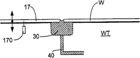
In the embodiment of Figure 4 and 5, an edge liquid-supplying system provides liquid via port 40 to liquid reservoir 30.Liquid in the liquid reservoir 30 can be identical with the immersion liquid in the liquid-supplying system.Liquid reservoir 30 is located at a substrate W side relative with projection lens, and the edge of the edge of adjacent substrate W and edge seal member 17,117.In Fig. 5, edge seal member 17 is made up of an element that separates with base station WT, otherwise in Fig. 4, edge seal member 117 is provided by base station WT part in aggregates.Can clearly be seen that from Fig. 4 substrate W is supported on the base station WT by a so-called projection platform 20.Projection platform 20 comprises substrate W support a plurality of outshots thereon.By for example vacuum source, thereby the upper surface that substrate is drawn onto base station WT keeps substrate W in position.By using liquid reservoir 30, when the imaging of the edge of substrate W, (promptly when the liquid in the liquid-supplying system under the projection lens is horizontally through basal edge), liquid can not be from liquid-supplying system spills into gap between edge seal member 17,117 and the substrate W, because this space full of liquid.
The mechanism 170 that remainder with respect to base station WT moves edge seal member 17 that is used for that is shown among Fig. 5 explains at Fig. 6.Mobile by this way edge seal member 17 is because the first type surface that can make its first type surface and substrate W coplane basically.This makes liquid-supplying system easy motion on the substrate W marginal portion, so that the bottom inner periphery of liquid-supplying system can move and makes its part be placed on the first type surface of substrate W and part is placed on the first type surface of edge seal member 17.
A horizon sensor (not shown) is used to survey the relative height of substrate W and edge seal member 17 first type surfaces.Based on the result of horizon sensor, transmit and control signal to the height of actuator 171 with the first type surface of adjustment edge seal member 17.Closed-loop actuators also can be used for this purpose.
When wedge-like part 172 as shown in Figure 6 left and when moving right, its top surface 175 (the wedge-like surface that tilts with respect to the first type surface of edge seal member 17) contact is fixed on the lower inclined surface of the additional wedge-like member 173 of edge seal member 17 bottoms.When wedge-like member 172 left and when moving right, edge seal member 17 reduces respectively and raises to prevent that edge seal member 17 from moving at the moving direction of wedge-like member 172.A little biasing of 17 basad WT of edge seal member is essential.
Clearly, additional wedge-like member 173 can replace with another kind of shape, for example the rhabodoid of placing perpendicular to the moving direction of wedge-like member 172.If the friction factor between wedge-like member 172 and the additional wedge-like member 173 is greater than the tangent value of the angle of wedge, then actuator 170 Braking mode mean that the power of need not puts on wedge-like member 172 to keep it in position.This is favourable, because when actuator 170 does not activate, this system will be stable.The precision of mechanism 170 is in several approximately micron dimensions.
Especially, under edge seal member 117 and base station WT situation in aggregates, mechanism can be used for adjusting the height of the member of substrate W or support base W, and the first type surface that makes edge seal member 17,117 and substrate is coplane basically.
Embodiment 3
The 3rd embodiment is shown among Fig. 7, and same or similar with first embodiment except that describing below.
Contact and base station WT edge seal member 117 in aggregates is described this embodiment.But this embodiment is equally applicable to the edge seal member 17 that can move with respect to base station WT.In this embodiment, edge seal member 17 has with the upper surface of substrate first type surface coplane optional, still, is preferred.The vacuum ports 46 that is connected to vacuum source is positioned at the bottom, and the marginal portion of joining edge containment member 117 and in the marginal portion of substrate W to the opposite side adjacent substrate W of projection system.Preferably, port 46 be annular and form by continuous groove, still, can be discontinuous, many discontinuous openings promptly are set in circular pattern.This embodiment can only pass through the vacuum work that port 46 is supplied with the simplest form.But,, can improve basic idea by the base station WT that is shown specifically as in Fig. 7 a of first kind of form representing the 3rd embodiment is provided.
The part 48 of base station WT is extended to internal radiation from the edge of edge seal member 117 is positioned at below the substrate W its opposite side at the relative projection system of substrate.Any immersion liquid by the gap seepage between part 48 and the substrate W is attracted to vacuum source via port 46.Passage 42 also under substrate W towards the vacuum source internal radiation and be connected to gas source.This gas can be pressure greater than the gas of atmospheric pressure or passage 42 simply to atmosphere opening.Be created between the part 48 of base station WT below the substrate W and the projection platform 20 below the substrate W to extraradial air-flow.(projection platform 20 has its oneself vacuum source so that substrate is kept in position).Because this air-flow, the liquid that overflows between any edge seal member 117 and the substrate W all is attracted to the annular and separation chamber 44 that is connected with the vacuum source fluid, and (xsect is approximately 3 * 3mm).Compartment 44 is to the open ring-type port 47 in gap and be connected between the port 46 of vacuum source.Compartment helps to set up evenly flowing around circumference.Passage 42 is connected to continuous annular groove (being shown the expansion of pipe).The groove of compartment 44, port 47 and/or passage 42 need not be ring-type and can be other suitable shape or configuration.
In a feasible embodiment, the part 48 of base station WT and the gap between the substrate W are 100 μ m magnitudes (although can not have the gap, be zero) at the most, because capillarity prevents that the liquid of high flow rate from passing the gap.The height of the part 45 of base station WT between groove that is connected to passage 42 and compartment 44 is the distance (representing with distance D 1 among Fig. 7) between the top of the bottom of substrate W and part 45, be typically 100 μ m magnitudes, the selection of distance make in the zone flow velocity at least the balanced air-flow of 1m/s can reach the pressure loss and be lower than 0.5bar.Such setting guarantees only to have the liquid of considerably less (if having) to pass clearance D 1 and little interference projection platform 20.Other numerical value also can.
The first kind of form that is shown in the 3rd embodiment among Fig. 7 a can be born the outwards approximately deflection of 10mm of substrate W.Can be as seen from Figure 7, this zone is all less than supporting, even as mentioned above, part 45 can extend to support base W place below the substrate W.But in more outside radius, the capillary force of water still can make the edge deflection of substrate W between the part 48 of the weight of substrate W and substrate W and base station WT.Significantly, this is harmful to.The solution of this problem is shown among Fig. 7 b-d of second to the 4th kind of form representing the 3rd embodiment.Identical Reference numeral is used for representing identical feature.
In second kind of form shown in Fig. 7 b, part 48 has at least one group and is positioned at around the joint (burl) 348 (according to circular pattern) of also close substrate W surrounding edge.Disperse because save 348, immersion liquid still can be between part 48 and substrate W seepage, but the weight of substrate W is supported by at least one group of joint 348.Preferably, joint 348 has the height littler than the joint of projection platform 20, projection platform 20 save the difference of power downward on the substrate W that compensation is caused by the vacuum 22 of projection platform 20 with respect near the power of substrate W coboundary joint 348.Must consider the hardness that saves during calculating, and if the low-expansion glass such as the Zerodur that save preferred use make, so, joint must be than the joint of projection platform 20 low about 80nm.The preferably about 20 μ m in gap between part 48 and the substrate W bottom.
In the form of Fig. 7 b, the shape of part 45 and first kind of form similar.But selectable joint 345 with ring-type or circular pattern is positioned on the part 45.The discontinuous characteristic of joint 345 makes the gas from passage 42 be inhaled into compartment 44.These joints 345 also hang down about 80nm than the joint of projection platform 20.Preferably, save clearance D 1 about 50 μ m of 345.Joint 345 can be formed by projection platform 20, and need not the ingredient into base station WT.
Can clearly be seen that from two kinds of forms of above-mentioned the 3rd embodiment the air impervious structure that is formed by passage 42 and 47 can be formed by base station WT fully, perhaps form by projection platform 20 fully that perhaps the combination by the two forms.Fig. 7 c and 7d illustrate two kinds of forms in addition of the 3rd embodiment.Fig. 7 c illustrates the third form that is formed air impervious the 3rd embodiment by the member of projection platform 20.The part 45 of first and second kinds of forms is formed by the annulus 2045 of projection platform, and the part 48 of first and second kinds of forms is formed by the annulus 2048 of projection platform 20. Passage 2042 and 2047 is equivalent to 42 and 47, forms between part 20,2045 and 2048.But only some air-flow passes two passages 2042 and 2047; As shown in the figure, some air-flow is below projection platform 20, and effectively the immersion liquid of obstruction seepage under projection platform 20 outer rims further enters.Such setting is favourable, because all essential accurate dimensions all form on projection platform 20, and base station WT does not comprise the groove of any complexity.
In Fig. 7 d of the 4th kind of form that the 3rd embodiment is shown, there is not access road 42, air-flow enters ring port 47 from projection platform 20.The advantage of this form is, because projection platform 20 does not need its oneself vacuum source, experiences more pressure stable between substrate W and projection platform 20.In addition, no longer need necessary additional channels 2047 in the third form, only need passage 2042.Like this, single vacuum source all is effective to removing the seepage immersion liquid and keeping substrate in position.Below projection platform 20, may need a gas source (the perhaps more common vacuum ports of base station below projection platform 20 can be used for this purpose), like this, can set up outside air-flow.
Clearly, just can make up the different characteristic of every kind of form of the 3rd embodiment as long as realize from the projection platform to extraradial air-flow to vacuum 46.
Embodiment 4
The 4th embodiment is shown among Fig. 8 and Fig. 9, and is same or similar with first embodiment except that describing below.
Contact and base station WT edge seal member 117 in aggregates is described this embodiment.But this embodiment is equally applicable to the edge seal member 17 that can move with respect to base station WT.
In the first kind of form of this embodiment shown in Fig. 8 a, additional edge seal member 500 is used for the gap between cross-over connection edge seal member 117 and the substrate W.Should additional edge seal member be installed on edge seal member 117.Additional edge seal member 500 is adhered to movably and is resisted against and substrate W first type surface apparent surface.In this embodiment, additional edge seal member 500 can be the elastic edge containment member of activatable contact substrate W lower surface.When elastic edge containment member 500 was inoperative, elastic edge containment member 500 left substrate and falls under action of gravity.The mode that realizes this action is shown among Fig. 9, and describes hereinafter.
Additional edge seal member 500 will can not prevent that probably the immersion liquid of all liq feed system from entering the space below the substrate W, therefore, in some or the form of ownership of this embodiment, the edge of joining edge containment member 117 and substrate W provides a port 46 that is connected to low pressure source below substrate W.Certainly, identical among the region design below the substrate and the 3rd embodiment.
Identical system is used in sensor rather than the substrate W on the base station, for example transmission image-position sensor (TIS).Under the situation of using sensor, because sensor does not move, edge seal member 500 can for good and all be attached to sensor, for example uses glue.
In addition, edge seal member 500 can be arranged to engage with the top surface (surface nearest with projection system) rather than the basal surface of object.Equally, additional edge seal member 500 can be attached to or keep to the side the top surface of containment member 117 rather than as shown in Fig. 8 a below edge seal member 117.
Second kind of form of this embodiment is shown among Fig. 8 b.Two additional edge seal member 500a, 500b have been used.Identical in the first edge seal member 500a and the first kind of form.The second edge seal member 500b is installed on base station 20, promptly below substrate W and its free end extend to external radiation from its mounting points.The second additional edge seal member 500b clamps the first additional edge seal member 500a against substrate W.Pressure gas can be used for making the second additional edge seal member 500b distortion or moves the second additional edge seal member 500b.
The third form of this embodiment is shown among Fig. 8 c.The third form is clamped the second edge seal member 500d except that the first additional basad W of edge seal member 500c, and is identical with second kind of form.This has been avoided, for example the demand of the pressure gas of second kind of form.
Be appreciated that this embodiment also will work under the situation that only has second additional edge seal member 500b, the 500d that connect or be not connected to vacuum.
Now, with the various methods that make additional edge seal member 500,500a, 500b, 500c, 500d distortion of first kind of formal description of contact embodiment.
As can be seen from Figure 9, passage 510 forms at the bearing of trend of the additional edge seal member 500 of elasticity (circle of preferred annular), and, one or more discrete ports are arranged at the upper surface that adds edge seal member towards the elasticity of projection system and substrate W bottom surface.By vacuum source 515 being connected to pipe 510, suction can make elasticity add edge seal member adjacent substrate W.When vacuum source 515 disconnected connection or closes, the additional edge seal member 500 of elasticity fell the position that is shown in broken lines among Fig. 9 to present under gravity and/or the pressure effect from port 46.
In another embodiment, the mechanical preload of additional edge seal member 500 usefulness of elasticity forms, make and to be placed on the projection platform 20 and elasticity when adding edge seal member 500 elastic deformations when substrate, the additional edge seal member 500 contact substrate W of elasticity, like this, the additional basad W of edge seal member of elasticity applies a power that makes progress, thereby forms sealing.
In another embodiment, the additional edge seal member 500 of elasticity is subjected to overvoltage that the gas-pressurized by port 46 produces and against substrate W.
The additional edge seal member 500 of elasticity can by any flexible, radioresistance and anti-immersion liquid, nonpollution material makes, for example, steel, glass such as Al
2O
3, stupalith such as SiC, silicon, teflon, low-expansion glass (as Zerodur (TM) or ULE (TM)), carbon fiber in epoxy or quartz, and typically thickness is 10~500 μ m, preferred 30~200 μ m are perhaps if glass then is 50~150 μ m.With the additional edge seal member 500 of the elasticity of this material and these sizes, the special pressure that need be applied to pipe 510 is approximately 0.1~0.6bar.
Embodiment 5
The 5th embodiment is shown among Figure 10, and is same or similar with first embodiment except that describing below.
This embodiment is in conjunction with describing with base station WT edge seal member 117 in aggregates.But this embodiment is equally applicable to the edge seal member 17 that can move with respect to base station WT.
In the 5th embodiment, fill with additional edge seal member 50 in the gap between edge seal member 117 and the substrate W.Should additional edge seal member be to have and the first type surface of substrate W and the edge seal member 117 additional edge seal member 50 of elasticity of the top surface of coplane basically.The additional edge seal member 50 of this elasticity is made by compliant material (compliant material), like this, can adapt to the subtle change of substrate W diameter and substrate W thickness by the deflection of the additional edge seal member 50 of elasticity.When the liquid in the liquid-supplying system at projection lens during below by basal edge, liquid can not overflow between substrate W, the additional edge seal member 50 of elasticity and edge seal member 117 because the edge of these elements tightly mutually against.In addition, because the top surface of the additional edge seal member 50 of the first type surface of substrate W and edge seal member 117 and elasticity is coplane basically, not chaotic through out-of-date liquid-supplying system running on the edge of liquid in substrate W, like this, in liquid-supplying system, do not produce perturbed force.
As can be seen from Figure 10, the additional edge seal member 50 of elasticity contacts with the substrate surface relative with the substrate W first type surface in the marginal portion.This contact has two kinds of effects.The first, improved the hydraulic seal between additional edge seal member 50 of elasticity and substrate W.The second, the additional edge seal member 50 of elasticity applies the power away from projection platform 20 directions on substrate W.When substrate W remained on the base station WT by for example pull of vacuum, substrate can remain on the base station reliably.But when closing vacuum source or not connecting vacuum source, the power that is produced on substrate W by the additional edge seal member 50 of elasticity promotes substrate W effectively and leaves base station WT, thereby has assisted the loading and the unloading of substrate W.
The additional edge seal member 50 of elasticity is made by the material such as the PTFE of radioresistance and anti-immersion liquid.
Embodiment 6
Figure 11 illustrates sixth embodiment of the invention, and this embodiment is same or similar with first embodiment except that describing below.
This embodiment is in conjunction with describing with base station WT edge seal member 117 in aggregates.But this embodiment is equally applicable to the edge seal member 17 that can move with respect to base station WT.
The 6th embodiment illustrate projection platform 20 be how with substrate W and edge seal member 117 between liquid-supplying system separate.This be by the edge of substrate W with substrate W is remained on the base station WT and and the vacuum that is associated in of projection platform 20 between place an opening that is exposed to atmosphere 65 and finish.
Embodiment 7
With reference to Figure 12~15 seventh embodiment of the present invention is described below.The 7th embodiment is same or similar with first embodiment except that describing below.
In the 7th embodiment, as shown in figure 12, edge seal member 17 is for having the annular greater than the center pit of circular-base W diameter.As long as the center pit of edge seal member 17 is greater than the external diameter of substrate W, the shape of substrate W and edge seal member 17 can change.Like this, edge seal member 17 can adapt to the substrate W diameter variation.
Can clearly be seen that from Figure 14 edge seal member 17 both can move in the main surface plane of substrate W, preferably can move in Z direction (promptly installing optical axis direction) again.Like this, edge seal member 17 can move to the edge of substrate W when needed, and has the height on the surface, top (master) of having proofreaied and correct, and the first type surface that makes its first type surface and substrate W is near coplane.This makes liquid-supplying system that immersion liquid is contained in its liquid reservoir effectively, even when to the edge imaging of substrate W.
Equally, being shown among Figure 14 is the outshot 175 that has with the top surface of edge seal member 17 first type surface coplanes, i.e. the overhanging adjacent substrate W in the edge of the first type surface of edge seal member 17 makes the optical axis extending of this teat branching unit.As can be seen from Figure 14, this makes the gap between the first type surface of substrate W and edge seal member 17 minimize, even when the edge of substrate W slight bending (edge of substrate W is not orthogonal to first type surface).
The another kind of method of improving and reducing the gap between edge seal member 17 and the substrate W is between the edge of close substrate W and the substrate W additional (elasticity) edge seal member 177 to be set in edge seal member 17, is shown among Figure 15.Outshot 175 can be arranged or do not have outshot 175.Added resilience edge seal member 177 can be around the edge deformation of substrate W, so that form the sealing closely of substrate W.This added resilience edge seal member 177 is attached to edge seal member 17.This added resilience edge seal member 177 has basically the upper surface with the first type surface coplane of substrate W and edge seal member 17.
Embodiment 8
Figure 16 illustrates eighth embodiment of the invention, and this embodiment is same or similar with first embodiment except that describing below.
This embodiment is in conjunction with describing with base station WT edge seal member 117 in aggregates.But this embodiment is equally applicable to the edge seal member 17 that can move with respect to base station WT.
As can be seen from Figure 16, the 8th embodiment comprises an additional edge seal member 100 that is used for the gap between cross-over connection edge seal member 117 and the substrate W.In this case, additional edge seal member 100 be on the first type surface of substrate W and edge seal member 117 with clearance seal member across the gap between substrate W and the edge seal member 117.Therefore, if substrate W is circular, clearance seal member 100 also will be circular (annular).
Advantageously, clearance seal member 100 has the tapered edge 110 that the thickness of clearance seal member 100 reduces to the edge.This transformation gradually up to clearance seal member 100 maximum ga(u)ges guarantee when liquid-supplying system by clearance seal member 100 on the time reduce the liquid-supplying system disturbance.
Identical encapsulating method can be used for for example sensor of other object, as the transmission image-position sensor.In this case, owing to do not need movement of objects, clearance sealing device 100 can be with not pasting (at arbitrary end) in position by dissolved gum in immersion liquid.Paste the abutment that selectively is positioned at edge seal member 117, object and clearance sealing device 100.
In addition, clearance sealing device 100 can be positioned at below the object and overhang on the edge seal member 117.If desired, this object also can be made and to dangle.
No matter clearance sealing device 100 is on object or below object, can have the passage that runs through its setting from a surface opening that contacts with edge seal member 117 to another surface opening that contacts with object.By an opening that links to each other in the liquid mode with vacuum 105 is set, clearance sealing device 100 just can be firmly held in suitable position.
Embodiment 9
With reference to Figure 17 the 9th embodiment is described below.The solution that is shown among Figure 17 has been avoided some problem about the marginal portion of imaging substrate W, makes simultaneously under the condition identical with substrate W with projection lens PL irradiation transmission image-position sensor (TIS).
The 9th embodiment adopts the liquid-supplying system of describing about first embodiment.But be not, but by intermediate plate 210 confined liquids between liquid-supplying system and substrate W with in the liquid-supplying system of immersion liquid its bottom side is limited in projection lens with substrate W below.Space 222,215 between intermediate plate 210 and TIS220 and substrate W is full of liquid 111 also.These can be by by two separated space liquid-supplying systems of port 230,240 separately, as shown in the figure, and perhaps by finishing by the same space liquid-supplying system of port 230,240.Like this, the space 220 between the space 215 between substrate W and the intermediate plate 210 and transmission image-position sensor 220 and intermediate plate 210 is full of liquid all, and substrate W can be shone under identical condition with the transmission image-position sensor.Part 200 provides a stayed surface or has been used for keeping by vacuum source the surface of intermediate plate in position.
This intermediate plate 210 is made such size, makes it cover substrate W and transmission image-position sensor 220 simultaneously.Like this, even when the imaging of the edge of substrate W or when below the transmission image-position sensor is positioned at projection lens PL, do not have the edge need pass liquid-supplying system yet.The top surface of transmission image-position sensor 220 and substrate W be coplane basically.
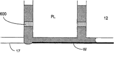
Figure 18 illustrates a kind of improvement that is applied to the liquid-supplying system of any other embodiment described herein, and this improvement has increased the size in the gap that immersion liquid can be crossed over before unexpected liquid loss effectively.
Between liquid-supplying system (for example containment member 12) and projection lens PL, a plurality of kapillaries 600 are arranged.These kapillaries extend generally upward, promptly away from substrate W.If radius capillaceous is r, can provide by following formula by the fluid film thickness h that kapillary supports:
Wherein, σ is an interfacial tension, and θ is liquid and intercapillary contact angle, and ρ is a fluid density.Like this, become on the occasion of (that is, it is hydrophobic that inside surface capillaceous is for example become by coating) by making cos θ, kapillary can be supported on and highly be a part of liquid of h on the gap, thereby crosses over bigger gap.
By between hydrophobic coating kapillary and liquid, applying voltage, cos θ can be reduced to and be approximately zero and make flow of liquid pass freely through kapillary 600 (according to above-mentioned formula), like this, by keeping capillary pipe length low, liquid can be removed the liquid-supplying system below projection lens at short notice.This helps keeping liquid clean.When the imaging of the edge of substrate W, can remove voltage and make liquid cross over the gap.In order to lift fluid film from substrate W, suggestion is with hydrophobic material coated substrate edge (perhaps when base material itself when being hydrophobic, can remove the resist on the substrate W edge).
All the foregoing descriptions can be used for sealing around the substrate W edge.Other object on base station WT also can seal with similar mode, for example comprise sensor and/or the sensor of mark, for example transmission image-position sensor, integral lens interferometer and scanner (Wavefront sensor) and point sensor plate with the projection fibers irradiation of passing liquid.These objects also comprise sensor and/or the mask with non-projection radiation bundle irradiation, for example measurement of the level and alignment sensor and/or mark.Under these circumstances, this liquid-supplying system can feed fluid to cover all objects.Embodiment above any may be used to this purpose.In some cases, do not need from base station WT remove object be because, form contrast with substrate W, sensor does not need to remove from base station.Under these circumstances, top embodiment can suitably improve (for example, sealing can need not to move).
Each embodiment can suitably combine with one or more other embodiment.In addition, the liquid-supplying system that is applied to not have in Fig. 2 and Figure 19 and 20 edge seal member 17,117 simply that each embodiment (with the combination of any suitable embodiment) equally can be reasonable and/or suitable.
The shape of edge seal member 117 and sensor 220 top outermost edges can be different.For example, provide a drape edge containment member 117 or even the outer rim of the sensor 220 that dangles be favourable.Perhaps, sensor 220 outside top angles are useful.
Figure 19 illustrates the 11 embodiment, and is identical with first embodiment except that describing below.
In the 11 embodiment, the object on base station WT is a sensor 220, as transmission image-position sensor (TIS).In order to prevent that immersion liquid from leaking into below the sensor 220, between edge seal member 117 and sensor 220, place one can not be dissolved in immersion liquid and with the nonreactive glue 700 of immersion liquid.In use, this glue is submerged the liquid covering.
With reference to Figure 20 and 21 the 12 embodiment is described.In the 12 embodiment, what be sealed to base station WT is sensor 220.In being shown in two kinds of forms of Figure 20 and 21, vacuum 46 is set in abutting connection with having the open channel 47 that is used to remove the liquid in gap between any edge that passes edge seal member 117 and substrate 220 and the gap of chamber 44.
In form shown in Figure 20, vacuum 46 be arranged on object 220 among the base station WT overhang below.Passage 47 is arranged in the outshot that base station WT inwardly dangles.Glue drips 700 and optionally is placed on the innermost edge of outshot between base station WT and the object 220.If there is not glue to drip 700, promote the sealing in gap between sensor 220 and the base station WT from object 220 following air-flows.
In the form of Figure 21, vacuum 46, compartment 44 and passage 47 are arranged in the object 220 self, below outstanding forward edge seal member 117.Equally, be chosen in that passage 47 radial outside placement glue drip between object 220 and the base station WT.
Below describe specific embodiments of the invention, be appreciated that the present invention except that above-mentioned, can adopt other modes to implement.Especially, the present invention can also be applied to other liquid-supplying system, especially the localized liquid district system.If use the containment member solution, can use the another kind sealing that is different from air seal.This explanation is not intended to limit the present invention.
Claims (11)
1. lithographic projection apparatus comprises:
Be used to support the supporting construction of patterning device, described patterning device is used for according to desirable pattern radiation laser beam being carried out composition;
Be used to keep the base station of substrate;
Be used for patterned light beam is projected projection system in the target portion of substrate.
Be used for the partially filled at least described projection system of liquid and described substrate or be placed on the described base station sensor or with the liquid-supplying system in described substrate and described sensor space between the two;
It is characterized in that, described base station also comprises to the edge of small part around described substrate, or the edge of described sensor, the edge seal member at the edge of perhaps described substrate and described sensor, and be arranged in a side direction described edge seal member and the described substrate relative with described projection system, or with described sensor, perhaps provide the vacuum ports of vacuum or liquid or liquid to supply with port with described substrate and described sensor gap between the two, wherein said base station also comprises a radial passage that is arranged on described vacuum ports inside, described passage is connected to gas source, can set up when the energized gas body source like this from described passage to described vacuum source to extraradial air-flow.
2. lithographic projection apparatus as claimed in claim 1, wherein the joint that contacts with described substrate distributes radially in described passage outside and in vacuum ports inside.
3. lithographic projection apparatus as claimed in claim 1, wherein said base station also are included in and stretch out below described substrate or described sensor or described substrate and the described sensor and in the outside radial part of described vacuum ports.
4. lithographic projection apparatus as claimed in claim 3, wherein said part has and extends upwardly to described substrate or to described sensor or to described substrate and described sensor, thereby supports the ingredient of described substrate or described sensor or described substrate and described sensor at least in part.
5. as each described lithographic projection apparatus in the claim 2 to 4, wherein said joint and/or part and/or ingredient are parts that supports the projection platform of described substrate.
6. as each described lithographic projection apparatus in the claim 1 to 4, also comprise by described vacuum ports link to each other in the liquid mode with described gap and with described base station that described vacuum source links to each other in the liquid mode in compartment.
7. as each described lithographic projection apparatus in the claim 1 to 4, wherein said vacuum ports is a ring-type.
8. as each described lithographic projection apparatus in the claim 1 to 4, wherein said vacuum ports is discontinuous.
9. as any one described lithographic projection apparatus among the claim 1-4, wherein said vacuum ports is continuous.
10. as each described lithographic projection apparatus in the claim 1 to 4, wherein said vacuum ports is set to the marginal portion of joining edge containment member.
11. as each described lithographic projection apparatus in the claim 1 to 4, the wherein said edge seal member or the first or second additional edge seal member are around pasting described substrate around described substrate or the described sensor, or described sensor, perhaps described substrate and described sensor, the wherein said first additional edge seal member be installed on edge seal member and the described edge seal member of cross-over connection and described substrate or and described sensor between the gap, described second adds that edge seal member is installed on described base station and its free end extends to external radiation from its mounting points.
Applications Claiming Priority (4)
| Application Number | Priority Date | Filing Date | Title |
|---|---|---|---|
| EP02257822 | 2002-11-12 | ||
| EP02257822.3 | 2002-11-12 | ||
| EP03253636.9 | 2003-06-09 | ||
| EP03253636 | 2003-06-09 |
Related Child Applications (1)
| Application Number | Title | Priority Date | Filing Date |
|---|---|---|---|
| CN2009102060966A Division CN101713932B (en) | 2002-11-12 | 2003-11-11 | Lithographic apparatus and device manufacturing method |
Publications (2)
| Publication Number | Publication Date |
|---|---|
| CN1501175A CN1501175A (en) | 2004-06-02 |
| CN100568101C true CN100568101C (en) | 2009-12-09 |
Family
ID=32852221
Family Applications (2)
| Application Number | Title | Priority Date | Filing Date |
|---|---|---|---|
| CN2009102060966A Expired - Lifetime CN101713932B (en) | 2002-11-12 | 2003-11-11 | Lithographic apparatus and device manufacturing method |
| CNB2003101233284A Expired - Lifetime CN100568101C (en) | 2002-11-12 | 2003-11-11 | Lithographic equipment and device making method |
Family Applications Before (1)
| Application Number | Title | Priority Date | Filing Date |
|---|---|---|---|
| CN2009102060966A Expired - Lifetime CN101713932B (en) | 2002-11-12 | 2003-11-11 | Lithographic apparatus and device manufacturing method |
Country Status (6)
| Country | Link |
|---|---|
| US (10) | US7199858B2 (en) |
| JP (4) | JP3953460B2 (en) |
| KR (1) | KR100588124B1 (en) |
| CN (2) | CN101713932B (en) |
| SG (1) | SG121819A1 (en) |
| TW (1) | TWI251127B (en) |
Families Citing this family (367)
| Publication number | Priority date | Publication date | Assignee | Title |
|---|---|---|---|---|
| US7240679B2 (en) * | 2002-09-30 | 2007-07-10 | Lam Research Corporation | System for substrate processing with meniscus, vacuum, IPA vapor, drying manifold |
| DE60335595D1 (en) * | 2002-11-12 | 2011-02-17 | Asml Netherlands Bv | Immersion lithographic apparatus and method of making a device |
| US7110081B2 (en) * | 2002-11-12 | 2006-09-19 | Asml Netherlands B.V. | Lithographic apparatus and device manufacturing method |
| CN101713932B (en) * | 2002-11-12 | 2012-09-26 | Asml荷兰有限公司 | Lithographic apparatus and device manufacturing method |
| US7372541B2 (en) * | 2002-11-12 | 2008-05-13 | Asml Netherlands B.V. | Lithographic apparatus and device manufacturing method |
| US9482966B2 (en) * | 2002-11-12 | 2016-11-01 | Asml Netherlands B.V. | Lithographic apparatus and device manufacturing method |
| JP3977324B2 (en) * | 2002-11-12 | 2007-09-19 | エーエスエムエル ネザーランズ ビー.ブイ. | Lithographic apparatus |
| US10503084B2 (en) | 2002-11-12 | 2019-12-10 | Asml Netherlands B.V. | Lithographic apparatus and device manufacturing method |
| SG121822A1 (en) * | 2002-11-12 | 2006-05-26 | Asml Netherlands Bv | Lithographic apparatus and device manufacturing method |
| EP1571698A4 (en) * | 2002-12-10 | 2006-06-21 | Nikon Corp | Exposure apparatus, exposure method and method for manufacturing device |
| US7948604B2 (en) * | 2002-12-10 | 2011-05-24 | Nikon Corporation | Exposure apparatus and method for producing device |
| EP1571694A4 (en) * | 2002-12-10 | 2008-10-15 | Nikon Corp | Exposure apparatus and method for manufacturing device |
| SG150388A1 (en) | 2002-12-10 | 2009-03-30 | Nikon Corp | Exposure apparatus and method for producing device |
| US7242455B2 (en) * | 2002-12-10 | 2007-07-10 | Nikon Corporation | Exposure apparatus and method for producing device |
| SG2011031200A (en) * | 2002-12-10 | 2014-09-26 | Nippon Kogaku Kk | Exposure apparatus and device manufacturing method |
| JP4352874B2 (en) * | 2002-12-10 | 2009-10-28 | 株式会社ニコン | Exposure apparatus and device manufacturing method |
| USRE46433E1 (en) * | 2002-12-19 | 2017-06-13 | Asml Netherlands B.V. | Method and device for irradiating spots on a layer |
| DE10261775A1 (en) | 2002-12-20 | 2004-07-01 | Carl Zeiss Smt Ag | Device for the optical measurement of an imaging system |
| KR20180126102A (en) * | 2003-02-26 | 2018-11-26 | 가부시키가이샤 니콘 | Exposure apparatus and method, and method of producing apparatus |
| KR101345474B1 (en) * | 2003-03-25 | 2013-12-27 | 가부시키가이샤 니콘 | Exposure system and device production method |
| ATE426914T1 (en) * | 2003-04-07 | 2009-04-15 | Nikon Corp | EXPOSURE APPARATUS AND METHOD FOR PRODUCING AN APPARATUS |
| KR20110104084A (en) | 2003-04-09 | 2011-09-21 | 가부시키가이샤 니콘 | Immersion lithography fluid control system |
| KR101346406B1 (en) | 2003-04-09 | 2014-01-02 | 가부시키가이샤 니콘 | Exposure method and apparatus, and device manufacturing method |
| EP1611482B1 (en) * | 2003-04-10 | 2015-06-03 | Nikon Corporation | Run-off path to collect liquid for an immersion lithography apparatus |
| JP4656057B2 (en) * | 2003-04-10 | 2011-03-23 | 株式会社ニコン | Electro-osmotic element for immersion lithography equipment |
| EP1611486B1 (en) * | 2003-04-10 | 2016-03-16 | Nikon Corporation | Environmental system including a transport region for an immersion lithography apparatus |
| WO2004090634A2 (en) * | 2003-04-10 | 2004-10-21 | Nikon Corporation | Environmental system including vaccum scavange for an immersion lithography apparatus |
| WO2004092830A2 (en) * | 2003-04-11 | 2004-10-28 | Nikon Corporation | Liquid jet and recovery system for immersion lithography |
| SG139736A1 (en) | 2003-04-11 | 2008-02-29 | Nikon Corp | Apparatus having an immersion fluid system configured to maintain immersion fluid in a gap adjacent an optical assembly |
| SG2013077797A (en) * | 2003-04-11 | 2017-02-27 | Nippon Kogaku Kk | Cleanup method for optics in immersion lithography |
| KR101369582B1 (en) | 2003-04-17 | 2014-03-04 | 가부시키가이샤 니콘 | Optical arrangement of autofocus elements for use with immersion lithography |
| TWI295414B (en) | 2003-05-13 | 2008-04-01 | Asml Netherlands Bv | Lithographic apparatus and device manufacturing method |
| CN100437358C (en) * | 2003-05-15 | 2008-11-26 | 株式会社尼康 | Exposure apparatus and device manufacturing method |
| TWI470671B (en) | 2003-05-23 | 2015-01-21 | 尼康股份有限公司 | Exposure method and exposure apparatus, and device manufacturing method |
| TW201806001A (en) | 2003-05-23 | 2018-02-16 | 尼康股份有限公司 | Exposure device and device manufacturing method |
| KR20110110320A (en) * | 2003-05-28 | 2011-10-06 | 가부시키가이샤 니콘 | Exposure method, exposure device, and device manufacturing method |
| TWI442694B (en) * | 2003-05-30 | 2014-06-21 | Asml Netherlands Bv | Lithographic apparatus and device manufacturing method |
| US7213963B2 (en) | 2003-06-09 | 2007-05-08 | Asml Netherlands B.V. | Lithographic apparatus and device manufacturing method |
| EP1486827B1 (en) | 2003-06-11 | 2011-11-02 | ASML Netherlands B.V. | Lithographic apparatus and device manufacturing method |
| US7317504B2 (en) * | 2004-04-08 | 2008-01-08 | Asml Netherlands B.V. | Lithographic apparatus and device manufacturing method |
| KR101290021B1 (en) | 2003-06-13 | 2013-07-30 | 가부시키가이샤 니콘 | Exposure method, substrate stage, exposure apparatus and method for manufacturing device |
| KR101931923B1 (en) | 2003-06-19 | 2018-12-21 | 가부시키가이샤 니콘 | Exposure device and device producing method |
| US6867844B2 (en) | 2003-06-19 | 2005-03-15 | Asml Holding N.V. | Immersion photolithography system and method using microchannel nozzles |
| US6809794B1 (en) * | 2003-06-27 | 2004-10-26 | Asml Holding N.V. | Immersion photolithography system and method using inverted wafer-projection optics interface |
| DE60321779D1 (en) * | 2003-06-30 | 2008-08-07 | Asml Netherlands Bv | Lithographic apparatus and method for making an article |
| JP2007527615A (en) * | 2003-07-01 | 2007-09-27 | 株式会社ニコン | Method of using isotope specific fluid as optical element |
| EP2466382B1 (en) * | 2003-07-08 | 2014-11-26 | Nikon Corporation | Wafer table for immersion lithography |
| KR101296501B1 (en) | 2003-07-09 | 2013-08-13 | 가부시키가이샤 니콘 | Exposure apparatus and method for manufacturing device |
| EP1643543B1 (en) * | 2003-07-09 | 2010-11-24 | Nikon Corporation | Exposure apparatus and method for manufacturing device |
| WO2005006415A1 (en) | 2003-07-09 | 2005-01-20 | Nikon Corporation | Exposure apparatus and method for manufacturing device |
| US7738074B2 (en) | 2003-07-16 | 2010-06-15 | Asml Netherlands B.V. | Lithographic apparatus and device manufacturing method |
| EP1500982A1 (en) | 2003-07-24 | 2005-01-26 | ASML Netherlands B.V. | Lithographic apparatus and device manufacturing method |
| JP4524669B2 (en) | 2003-07-25 | 2010-08-18 | 株式会社ニコン | Projection optical system inspection method and inspection apparatus |
| US7326522B2 (en) | 2004-02-11 | 2008-02-05 | Asml Netherlands B.V. | Device manufacturing method and a substrate |
| CN102043350B (en) | 2003-07-28 | 2014-01-29 | 株式会社尼康 | Exposure apparatus, device manufacturing method, and control method of exposure apparatus |
| EP1503244A1 (en) | 2003-07-28 | 2005-02-02 | ASML Netherlands B.V. | Lithographic projection apparatus and device manufacturing method |
| US7779781B2 (en) | 2003-07-31 | 2010-08-24 | Asml Netherlands B.V. | Lithographic apparatus and device manufacturing method |
| KR101769722B1 (en) | 2003-08-21 | 2017-08-18 | 가부시키가이샤 니콘 | Exposure apparatus, exposure method, and device producing method |
| SG133590A1 (en) | 2003-08-26 | 2007-07-30 | Nikon Corp | Optical element and exposure device |
| US8149381B2 (en) | 2003-08-26 | 2012-04-03 | Nikon Corporation | Optical element and exposure apparatus |
| CN101303536B (en) * | 2003-08-29 | 2011-02-09 | 株式会社尼康 | Exposure apparatus and device producing method |
| TWI263859B (en) | 2003-08-29 | 2006-10-11 | Asml Netherlands Bv | Lithographic apparatus and device manufacturing method |
| TWI622083B (en) * | 2003-08-29 | 2018-04-21 | Nikon Corp | Exposure apparatus, liquid removal method, and component manufacturing method |
| TWI245163B (en) | 2003-08-29 | 2005-12-11 | Asml Netherlands Bv | Lithographic apparatus and device manufacturing method |
| EP2261740B1 (en) | 2003-08-29 | 2014-07-09 | ASML Netherlands BV | Lithographic apparatus |
| EP3223074A1 (en) | 2003-09-03 | 2017-09-27 | Nikon Corporation | Apparatus and method for immersion lithography for recovering fluid |
| CN100394244C (en) * | 2003-09-03 | 2008-06-11 | 株式会社尼康 | Apparatus and method for providing fluid for immersion lithography |
| JP4444920B2 (en) * | 2003-09-19 | 2010-03-31 | 株式会社ニコン | Exposure apparatus and device manufacturing method |
| EP2312395B1 (en) * | 2003-09-29 | 2015-05-13 | Nikon Corporation | Exposure apparatus, exposure method, and method for producing a device |
| US7158211B2 (en) * | 2003-09-29 | 2007-01-02 | Asml Netherlands B.V. | Lithographic apparatus and device manufacturing method |
| EP1519231B1 (en) * | 2003-09-29 | 2005-12-21 | ASML Netherlands B.V. | Lithographic apparatus and device manufacturing method |
| EP1672682A4 (en) | 2003-10-08 | 2008-10-15 | Zao Nikon Co Ltd | Substrate transporting apparatus and method, exposure apparatus and method, and device producing method |
| EP1672681B8 (en) | 2003-10-08 | 2011-09-21 | Miyagi Nikon Precision Co., Ltd. | Exposure apparatus, substrate carrying method, exposure method, and method for producing device |
| JP2005136364A (en) * | 2003-10-08 | 2005-05-26 | Zao Nikon Co Ltd | Substrate carrying device, exposure device and device manufacturing method |
| TWI598934B (en) | 2003-10-09 | 2017-09-11 | Nippon Kogaku Kk | Exposure apparatus, exposure method, and device manufacturing method |
| EP1524557A1 (en) * | 2003-10-15 | 2005-04-20 | ASML Netherlands B.V. | Lithographic apparatus and device manufacturing method |
| EP1524558A1 (en) * | 2003-10-15 | 2005-04-20 | ASML Netherlands B.V. | Lithographic apparatus and device manufacturing method |
| TWI609409B (en) | 2003-10-28 | 2017-12-21 | 尼康股份有限公司 | Optical illumination device, exposure device, exposure method and device manufacturing method |
| US7352433B2 (en) | 2003-10-28 | 2008-04-01 | Asml Netherlands B.V. | Lithographic apparatus and device manufacturing method |
| US7411653B2 (en) * | 2003-10-28 | 2008-08-12 | Asml Netherlands B.V. | Lithographic apparatus |
| JP2005159322A (en) * | 2003-10-31 | 2005-06-16 | Nikon Corp | Surface plate, stage apparatus, exposure device and exposing method |
| EP1679737A4 (en) | 2003-10-31 | 2008-01-30 | Nikon Corp | Exposure apparatus and device producing method |
| JP4295712B2 (en) | 2003-11-14 | 2009-07-15 | エーエスエムエル ネザーランズ ビー.ブイ. | Lithographic apparatus and apparatus manufacturing method |
| TWI612338B (en) | 2003-11-20 | 2018-01-21 | 尼康股份有限公司 | Optical illuminating apparatus, exposure device, exposure method, and device manufacturing method |
| EP1695148B1 (en) * | 2003-11-24 | 2015-10-28 | Carl Zeiss SMT GmbH | Immersion objective |
| US7545481B2 (en) | 2003-11-24 | 2009-06-09 | Asml Netherlands B.V. | Lithographic apparatus and device manufacturing method |
| JP4513534B2 (en) * | 2003-12-03 | 2010-07-28 | 株式会社ニコン | Exposure apparatus, exposure method, and device manufacturing method |
| CN1890779B (en) * | 2003-12-03 | 2011-06-08 | 株式会社尼康 | Exposure apparatus, exposure method, device producing method |
| KR20170107102A (en) | 2003-12-03 | 2017-09-22 | 가부시키가이샤 니콘 | Exposure apparatus, exposure method, device producing method, and optical component |
| JP2005175016A (en) * | 2003-12-08 | 2005-06-30 | Canon Inc | Substrate holding device, exposure device using the same, and method of manufacturing device |
| JPWO2005057635A1 (en) * | 2003-12-15 | 2007-07-05 | 株式会社ニコン | Projection exposure apparatus, stage apparatus, and exposure method |
| EP1699073B1 (en) | 2003-12-15 | 2010-12-08 | Nikon Corporation | Stage system, exposure apparatus and exposure method |
| US20070081133A1 (en) * | 2004-12-14 | 2007-04-12 | Niikon Corporation | Projection exposure apparatus and stage unit, and exposure method |
| WO2005059977A1 (en) * | 2003-12-16 | 2005-06-30 | Nikon Corporation | Stage apparatus, exposure apparatus, and exposure method |
| US7394521B2 (en) * | 2003-12-23 | 2008-07-01 | Asml Netherlands B.V. | Lithographic apparatus and device manufacturing method |
| US7589818B2 (en) * | 2003-12-23 | 2009-09-15 | Asml Netherlands B.V. | Lithographic apparatus, alignment apparatus, device manufacturing method, and a method of converting an apparatus |
| JP2005191394A (en) * | 2003-12-26 | 2005-07-14 | Canon Inc | Exposing method and equipment |
| EP1703548B1 (en) * | 2004-01-05 | 2010-05-12 | Nikon Corporation | Exposure apparatus, exposure method, and device producing method |
| JP4572539B2 (en) * | 2004-01-19 | 2010-11-04 | 株式会社ニコン | Exposure apparatus, exposure method, and device manufacturing method |
| JP4843503B2 (en) * | 2004-01-20 | 2011-12-21 | カール・ツァイス・エスエムティー・ゲーエムベーハー | Microlithographic projection exposure apparatus and measuring apparatus for projection lens |
| US7589822B2 (en) | 2004-02-02 | 2009-09-15 | Nikon Corporation | Stage drive method and stage unit, exposure apparatus, and device manufacturing method |
| KR101227211B1 (en) | 2004-02-03 | 2013-01-28 | 가부시키가이샤 니콘 | Exposure apparatus and method of producing device |
| WO2005076324A1 (en) * | 2004-02-04 | 2005-08-18 | Nikon Corporation | Exposure apparatus, exposure method, and device producing method |
| TW201809727A (en) | 2004-02-06 | 2018-03-16 | 日商尼康股份有限公司 | Polarization changing device |
| US7050146B2 (en) | 2004-02-09 | 2006-05-23 | Asml Netherlands B.V. | Lithographic apparatus and device manufacturing method |
| US20070030467A1 (en) * | 2004-02-19 | 2007-02-08 | Nikon Corporation | Exposure apparatus, exposure method, and device fabricating method |
| WO2005081290A1 (en) * | 2004-02-19 | 2005-09-01 | Nikon Corporation | Exposure apparatus and method of producing the device |
| US20070166639A1 (en) * | 2004-02-20 | 2007-07-19 | Takayuki Araki | Laminated resist used for immersion lithography |
| JP4973754B2 (en) * | 2004-03-04 | 2012-07-11 | 株式会社ニコン | Exposure method, exposure apparatus, and device manufacturing method |
| JP4622340B2 (en) * | 2004-03-04 | 2011-02-02 | 株式会社ニコン | Exposure apparatus and device manufacturing method |
| JP2005259870A (en) * | 2004-03-10 | 2005-09-22 | Nikon Corp | Substrate retainer, stage device, exposing device and exposing method |
| KR101250155B1 (en) | 2004-03-25 | 2013-04-05 | 가부시키가이샤 니콘 | Exposure apparatus and method for manufacturing device |
| WO2005093792A1 (en) * | 2004-03-25 | 2005-10-06 | Nikon Corporation | Exposure equipment, exposure method and device manufacturing method |
| US7034917B2 (en) * | 2004-04-01 | 2006-04-25 | Asml Netherlands B.V. | Lithographic apparatus, device manufacturing method and device manufactured thereby |
| JP2005302880A (en) * | 2004-04-08 | 2005-10-27 | Canon Inc | Immersion aligner |
| US7898642B2 (en) * | 2004-04-14 | 2011-03-01 | Asml Netherlands B.V. | Lithographic apparatus and device manufacturing method |
| US7379159B2 (en) | 2004-05-03 | 2008-05-27 | Asml Netherlands B.V. | Lithographic apparatus and device manufacturing method |
| US8054448B2 (en) * | 2004-05-04 | 2011-11-08 | Nikon Corporation | Apparatus and method for providing fluid for immersion lithography |
| US7616383B2 (en) | 2004-05-18 | 2009-11-10 | Asml Netherlands B.V. | Lithographic apparatus and device manufacturing method |
| US7486381B2 (en) * | 2004-05-21 | 2009-02-03 | Asml Netherlands B.V. | Lithographic apparatus and device manufacturing method |
| KR101264936B1 (en) * | 2004-06-04 | 2013-05-15 | 가부시키가이샤 니콘 | Exposure apparatus exposure method and device producing method |
| JP4517341B2 (en) * | 2004-06-04 | 2010-08-04 | 株式会社ニコン | Exposure apparatus, nozzle member, and device manufacturing method |
| KR101368523B1 (en) | 2004-06-04 | 2014-02-27 | 칼 짜이스 에스엠테 게엠베하 | System for measuring the image quality of an optical imaging system |
| CN102290364B (en) | 2004-06-09 | 2016-01-13 | 尼康股份有限公司 | Base plate keeping device, the exposure device possessing it, manufacturing method |
| JP4826146B2 (en) * | 2004-06-09 | 2011-11-30 | 株式会社ニコン | Exposure apparatus and device manufacturing method |
| CN101819386B (en) * | 2004-06-09 | 2013-10-09 | 尼康股份有限公司 | Exposure apparatus and device manufacturing method |
| US8373843B2 (en) | 2004-06-10 | 2013-02-12 | Nikon Corporation | Exposure apparatus, exposure method, and method for producing device |
| US8717533B2 (en) * | 2004-06-10 | 2014-05-06 | Nikon Corporation | Exposure apparatus, exposure method, and method for producing device |
| EP2624282B1 (en) | 2004-06-10 | 2017-02-08 | Nikon Corporation | Immersion exposure apparatus and method, and methods for producing a device |
| US8508713B2 (en) * | 2004-06-10 | 2013-08-13 | Nikon Corporation | Exposure apparatus, exposure method, and method for producing device |
| SG153820A1 (en) | 2004-06-10 | 2009-07-29 | Nikon Corp | Exposure apparatus, exposure method, and device producing method |
| JP5130609B2 (en) * | 2004-06-10 | 2013-01-30 | 株式会社ニコン | Exposure apparatus, exposure method, and device manufacturing method |
| US20070222959A1 (en) * | 2004-06-10 | 2007-09-27 | Nikon Corporation | Exposure apparatus, exposure method, and method for producing device |
| US7481867B2 (en) * | 2004-06-16 | 2009-01-27 | Edwards Limited | Vacuum system for immersion photolithography |
| EP3255652B1 (en) * | 2004-06-21 | 2018-07-25 | Nikon Corporation | Exposure apparatus, exposure method and device manufacturing method |
| KR101330922B1 (en) | 2004-06-21 | 2013-11-18 | 가부시키가이샤 니콘 | Exposure equipment and device manufacturing method |
| US8698998B2 (en) * | 2004-06-21 | 2014-04-15 | Nikon Corporation | Exposure apparatus, method for cleaning member thereof, maintenance method for exposure apparatus, maintenance device, and method for producing device |
| US7517639B2 (en) | 2004-06-23 | 2009-04-14 | Taiwan Semiconductor Manufacturing Co., Ltd. | Seal ring arrangements for immersion lithography systems |
| US7501226B2 (en) * | 2004-06-23 | 2009-03-10 | Taiwan Semiconductor Manufacturing Co., Ltd. | Immersion lithography system with wafer sealing mechanisms |
| US7463330B2 (en) | 2004-07-07 | 2008-12-09 | Asml Netherlands B.V. | Lithographic apparatus and device manufacturing method |
| DE102004033208B4 (en) * | 2004-07-09 | 2010-04-01 | Vistec Semiconductor Systems Gmbh | Device for inspecting a microscopic component with an immersion objective |
| EP1780772B1 (en) * | 2004-07-12 | 2009-09-02 | Nikon Corporation | Exposure equipment and device manufacturing method |
| US7161663B2 (en) * | 2004-07-22 | 2007-01-09 | Asml Netherlands B.V. | Lithographic apparatus |
| EP3267257B1 (en) * | 2004-08-03 | 2019-02-13 | Nikon Corporation | Exposure apparatus, exposure method, and method for producing device |
| US7304715B2 (en) | 2004-08-13 | 2007-12-04 | Asml Netherlands B.V. | Lithographic apparatus and device manufacturing method |
| KR20070048164A (en) * | 2004-08-18 | 2007-05-08 | 가부시키가이샤 니콘 | Exposure apparatus and device manufacturing method |
| US7701550B2 (en) * | 2004-08-19 | 2010-04-20 | Asml Netherlands B.V. | Lithographic apparatus and device manufacturing method |
| US20060044533A1 (en) * | 2004-08-27 | 2006-03-02 | Asmlholding N.V. | System and method for reducing disturbances caused by movement in an immersion lithography system |
| US20070252970A1 (en) * | 2004-09-01 | 2007-11-01 | Nikon Corporation | Substrate Holder, Stage Apparatus, and Exposure Apparatus |
| WO2006030910A1 (en) * | 2004-09-17 | 2006-03-23 | Nikon Corporation | Substrate for exposure, exposure method and device manufacturing method |
| SG188899A1 (en) * | 2004-09-17 | 2013-04-30 | Nikon Corp | Substrate holding device, exposure apparatus, and device manufacturing method |
| US7522261B2 (en) * | 2004-09-24 | 2009-04-21 | Asml Netherlands B.V. | Lithographic apparatus and device manufacturing method |
| US7355674B2 (en) * | 2004-09-28 | 2008-04-08 | Asml Netherlands B.V. | Lithographic apparatus, device manufacturing method and computer program product |
| US7894040B2 (en) * | 2004-10-05 | 2011-02-22 | Asml Netherlands B.V. | Lithographic apparatus and device manufacturing method |
| US7209213B2 (en) * | 2004-10-07 | 2007-04-24 | Asml Netherlands B.V. | Lithographic apparatus and device manufacturing method |
| US7456929B2 (en) * | 2004-10-15 | 2008-11-25 | Nikon Corporation | Exposure apparatus and device manufacturing method |
| JP4625673B2 (en) * | 2004-10-15 | 2011-02-02 | 株式会社東芝 | Exposure method and exposure apparatus |
| US7119876B2 (en) * | 2004-10-18 | 2006-10-10 | Asml Netherlands B.V. | Lithographic apparatus and device manufacturing method |
| US7379155B2 (en) | 2004-10-18 | 2008-05-27 | Asml Netherlands B.V. | Lithographic apparatus and device manufacturing method |
| WO2006047127A1 (en) * | 2004-10-21 | 2006-05-04 | Saint-Gobain Ceramics & Plastics, Inc. | Optical lens elements, semiconductor lithographic patterning apparatus, and methods for processing semiconductor devices |
| CN101866113B (en) * | 2004-10-26 | 2013-04-24 | 株式会社尼康 | Method of processing substrate, exposure device and method of manufacturing device |
| JP4848956B2 (en) | 2004-11-01 | 2011-12-28 | 株式会社ニコン | Exposure apparatus, exposure method, and device manufacturing method |
| US7583357B2 (en) | 2004-11-12 | 2009-09-01 | Asml Netherlands B.V. | Lithographic apparatus and device manufacturing method |
| US7414699B2 (en) * | 2004-11-12 | 2008-08-19 | Asml Netherlands B.V. | Lithographic apparatus and device manufacturing method |
| US7423720B2 (en) | 2004-11-12 | 2008-09-09 | Asml Netherlands B.V. | Lithographic apparatus and device manufacturing method |
| US7251013B2 (en) | 2004-11-12 | 2007-07-31 | Asml Netherlands B.V. | Lithographic apparatus and device manufacturing method |
| US7411657B2 (en) | 2004-11-17 | 2008-08-12 | Asml Netherlands B.V. | Lithographic apparatus and device manufacturing method |
| TWI393170B (en) * | 2004-11-18 | 2013-04-11 | 尼康股份有限公司 | A position measuring method, a position control method, a measuring method, a loading method, an exposure method, an exposure apparatus, and a device manufacturing method |
| US7230681B2 (en) * | 2004-11-18 | 2007-06-12 | International Business Machines Corporation | Method and apparatus for immersion lithography |
| US7362412B2 (en) * | 2004-11-18 | 2008-04-22 | International Business Machines Corporation | Method and apparatus for cleaning a semiconductor substrate in an immersion lithography system |
| EP1814146A4 (en) * | 2004-11-19 | 2009-02-11 | Nikon Corp | Maintenance method, exposure method, exposure apparatus, and device producing method |
| US7145630B2 (en) * | 2004-11-23 | 2006-12-05 | Asml Netherlands B.V. | Lithographic apparatus and device manufacturing method |
| US7256121B2 (en) * | 2004-12-02 | 2007-08-14 | Texas Instruments Incorporated | Contact resistance reduction by new barrier stack process |
| US7161654B2 (en) * | 2004-12-02 | 2007-01-09 | Asml Netherlands B.V. | Lithographic apparatus and device manufacturing method |
| US7446850B2 (en) * | 2004-12-03 | 2008-11-04 | Asml Netherlands B.V. | Lithographic apparatus and device manufacturing method |
| US7196770B2 (en) * | 2004-12-07 | 2007-03-27 | Asml Netherlands B.V. | Prewetting of substrate before immersion exposure |
| US7248334B2 (en) * | 2004-12-07 | 2007-07-24 | Asml Netherlands B.V. | Sensor shield |
| US7397533B2 (en) * | 2004-12-07 | 2008-07-08 | Asml Netherlands B.V. | Lithographic apparatus and device manufacturing method |
| US7365827B2 (en) | 2004-12-08 | 2008-04-29 | Asml Netherlands B.V. | Lithographic apparatus and device manufacturing method |
| US7352440B2 (en) | 2004-12-10 | 2008-04-01 | Asml Netherlands B.V. | Substrate placement in immersion lithography |
| KR101939525B1 (en) * | 2004-12-15 | 2019-01-16 | 가부시키가이샤 니콘 | Substrate holding apparatus, exposure apparatus and device manufacturing method |
| US7403261B2 (en) * | 2004-12-15 | 2008-07-22 | Asml Netherlands B.V. | Lithographic apparatus and device manufacturing method |
| JP2006173527A (en) * | 2004-12-20 | 2006-06-29 | Sony Corp | Exposure equipment |
| US7880860B2 (en) * | 2004-12-20 | 2011-02-01 | Asml Netherlands B.V. | Lithographic apparatus and device manufacturing method |
| US7528931B2 (en) | 2004-12-20 | 2009-05-05 | Asml Netherlands B.V. | Lithographic apparatus and device manufacturing method |
| US7405805B2 (en) | 2004-12-28 | 2008-07-29 | Asml Netherlands B.V. | Lithographic apparatus and device manufacturing method |
| US7491661B2 (en) * | 2004-12-28 | 2009-02-17 | Asml Netherlands B.V. | Device manufacturing method, top coat material and substrate |
| US20060147821A1 (en) | 2004-12-30 | 2006-07-06 | Asml Netherlands B.V. | Lithographic apparatus and device manufacturing method |
| US7450217B2 (en) * | 2005-01-12 | 2008-11-11 | Asml Netherlands B.V. | Exposure apparatus, coatings for exposure apparatus, lithographic apparatus, device manufacturing method, and device manufactured thereby |
| DE602006012746D1 (en) | 2005-01-14 | 2010-04-22 | Asml Netherlands Bv | Lithographic apparatus and manufacturing method |
| SG124351A1 (en) | 2005-01-14 | 2006-08-30 | Asml Netherlands Bv | Lithographic apparatus and device manufacturing method |
| JP2006202825A (en) * | 2005-01-18 | 2006-08-03 | Jsr Corp | Immersion type exposure device |
| WO2006078292A1 (en) * | 2005-01-21 | 2006-07-27 | Nikon Corporation | Offset partial ring seal in immersion lithographic system |
| US20090262316A1 (en) * | 2005-01-31 | 2009-10-22 | Nikon Corporation | Exposure apparatus and method for producing device |
| US8692973B2 (en) * | 2005-01-31 | 2014-04-08 | Nikon Corporation | Exposure apparatus and method for producing device |
| CN102360170B (en) | 2005-02-10 | 2014-03-12 | Asml荷兰有限公司 | Immersion liquid, exposure apparatus, and exposure process |
| US20070258068A1 (en) * | 2005-02-17 | 2007-11-08 | Hiroto Horikawa | Exposure Apparatus, Exposure Method, and Device Fabricating Method |
| US8018573B2 (en) * | 2005-02-22 | 2011-09-13 | Asml Netherlands B.V. | Lithographic apparatus and device manufacturing method |
| US7224431B2 (en) * | 2005-02-22 | 2007-05-29 | Asml Netherlands B.V. | Lithographic apparatus and device manufacturing method |
| US7378025B2 (en) | 2005-02-22 | 2008-05-27 | Asml Netherlands B.V. | Fluid filtration method, fluid filtered thereby, lithographic apparatus and device manufacturing method |
| JP2006270057A (en) * | 2005-02-28 | 2006-10-05 | Canon Inc | Aligner |
| US7282701B2 (en) * | 2005-02-28 | 2007-10-16 | Asml Netherlands B.V. | Sensor for use in a lithographic apparatus |
| US7428038B2 (en) * | 2005-02-28 | 2008-09-23 | Asml Netherlands B.V. | Lithographic apparatus, device manufacturing method and apparatus for de-gassing a liquid |
| US7324185B2 (en) | 2005-03-04 | 2008-01-29 | Asml Netherlands B.V. | Lithographic apparatus and device manufacturing method |
| US7684010B2 (en) * | 2005-03-09 | 2010-03-23 | Asml Netherlands B.V. | Lithographic apparatus, device manufacturing method, seal structure, method of removing an object and a method of sealing |
| TWI424260B (en) * | 2005-03-18 | 2014-01-21 | 尼康股份有限公司 | A board member, a substrate holding device, an exposure apparatus and an exposure method, and a device manufacturing method |
| US7330238B2 (en) * | 2005-03-28 | 2008-02-12 | Asml Netherlands, B.V. | Lithographic apparatus, immersion projection apparatus and device manufacturing method |
| US7411654B2 (en) | 2005-04-05 | 2008-08-12 | Asml Netherlands B.V. | Lithographic apparatus and device manufacturing method |
| USRE43576E1 (en) | 2005-04-08 | 2012-08-14 | Asml Netherlands B.V. | Dual stage lithographic apparatus and device manufacturing method |
| US7291850B2 (en) * | 2005-04-08 | 2007-11-06 | Asml Netherlands B.V. | Lithographic apparatus and device manufacturing method |
| US20060232753A1 (en) * | 2005-04-19 | 2006-10-19 | Asml Holding N.V. | Liquid immersion lithography system with tilted liquid flow |
| EP1876635A4 (en) | 2005-04-25 | 2010-06-30 | Nikon Corp | Exposure method, exposure apparatus and device manufacturing method |
| JP4752320B2 (en) * | 2005-04-28 | 2011-08-17 | 株式会社ニコン | Substrate holding apparatus and exposure apparatus, substrate holding method, exposure method, and device manufacturing method |
| EP1876637A4 (en) | 2005-04-28 | 2010-01-27 | Nikon Corp | Exposure method, exposure apparatus and device manufacturing method |
| US8248577B2 (en) * | 2005-05-03 | 2012-08-21 | Asml Netherlands B.V. | Lithographic apparatus and device manufacturing method |
| US7317507B2 (en) * | 2005-05-03 | 2008-01-08 | Asml Netherlands B.V. | Lithographic apparatus and device manufacturing method |
| US7433016B2 (en) | 2005-05-03 | 2008-10-07 | Asml Netherlands B.V. | Lithographic apparatus and device manufacturing method |
| KR101504765B1 (en) | 2005-05-12 | 2015-03-30 | 가부시키가이샤 니콘 | Projection optical system, exposure apparatus and exposure method |
| JP2006339448A (en) | 2005-06-02 | 2006-12-14 | Canon Inc | Exposure device with photodetection unit |
| JP4708876B2 (en) * | 2005-06-21 | 2011-06-22 | キヤノン株式会社 | Immersion exposure equipment |
| US7751027B2 (en) | 2005-06-21 | 2010-07-06 | Asml Netherlands B.V. | Lithographic apparatus and device manufacturing method |
| US7652746B2 (en) * | 2005-06-21 | 2010-01-26 | Asml Netherlands B.V. | Lithographic apparatus and device manufacturing method |
| US7468779B2 (en) * | 2005-06-28 | 2008-12-23 | Asml Netherlands B.V. | Lithographic apparatus and device manufacturing method |
| US7834974B2 (en) | 2005-06-28 | 2010-11-16 | Asml Netherlands B.V. | Lithographic apparatus and device manufacturing method |
| US7474379B2 (en) * | 2005-06-28 | 2009-01-06 | Asml Netherlands B.V. | Lithographic apparatus and device manufacturing method |
| US7170583B2 (en) * | 2005-06-29 | 2007-01-30 | Asml Netherlands B.V. | Lithographic apparatus immersion damage control |
| US7535644B2 (en) * | 2005-08-12 | 2009-05-19 | Asml Netherlands B.V. | Lens element, lithographic apparatus, device manufacturing method, and device manufactured thereby |
| US8054445B2 (en) * | 2005-08-16 | 2011-11-08 | Asml Netherlands B.V. | Lithographic apparatus and device manufacturing method |
| US7751026B2 (en) * | 2005-08-25 | 2010-07-06 | Nikon Corporation | Apparatus and method for recovering fluid for immersion lithography |
| US7357768B2 (en) * | 2005-09-22 | 2008-04-15 | William Marshall | Recliner exerciser |
| US8202460B2 (en) * | 2005-09-22 | 2012-06-19 | International Business Machines Corporation | Microelectronic substrate having removable edge extension element |
| JP3997244B2 (en) * | 2005-10-04 | 2007-10-24 | キヤノン株式会社 | Exposure apparatus and device manufacturing method |
| JP3997245B2 (en) * | 2005-10-04 | 2007-10-24 | キヤノン株式会社 | Exposure apparatus and device manufacturing method |
| US7411658B2 (en) | 2005-10-06 | 2008-08-12 | Asml Netherlands B.V. | Lithographic apparatus and device manufacturing method |
| JP4125315B2 (en) * | 2005-10-11 | 2008-07-30 | キヤノン株式会社 | Exposure apparatus and device manufacturing method |
| JP2007123525A (en) * | 2005-10-27 | 2007-05-17 | Toshiba Corp | Immersion exposure device and manufacturing method of semiconductor device |
| KR20080066836A (en) * | 2005-11-09 | 2008-07-16 | 가부시키가이샤 니콘 | Exposure apparatus, exposure method and device manufacturing method |
| US7656501B2 (en) * | 2005-11-16 | 2010-02-02 | Asml Netherlands B.V. | Lithographic apparatus |
| US7864292B2 (en) * | 2005-11-16 | 2011-01-04 | Asml Netherlands B.V. | Lithographic apparatus and device manufacturing method |
| US7804577B2 (en) | 2005-11-16 | 2010-09-28 | Asml Netherlands B.V. | Lithographic apparatus |
| US7633073B2 (en) * | 2005-11-23 | 2009-12-15 | Asml Netherlands B.V. | Lithographic apparatus and device manufacturing method |
| US7773195B2 (en) * | 2005-11-29 | 2010-08-10 | Asml Holding N.V. | System and method to increase surface tension and contact angle in immersion lithography |
| US8125610B2 (en) * | 2005-12-02 | 2012-02-28 | ASML Metherlands B.V. | Method for preventing or reducing contamination of an immersion type projection apparatus and an immersion type lithographic apparatus |
| US20070124987A1 (en) * | 2005-12-05 | 2007-06-07 | Brown Jeffrey K | Electronic pest control apparatus |
| KR100768849B1 (en) * | 2005-12-06 | 2007-10-22 | 엘지전자 주식회사 | Power supply apparatus and method for line conection type fuel cell system |
| TWI406321B (en) | 2005-12-08 | 2013-08-21 | 尼康股份有限公司 | A substrate holding device, an exposure apparatus, an exposure method, and an element manufacturing method |
| US7420194B2 (en) * | 2005-12-27 | 2008-09-02 | Asml Netherlands B.V. | Lithographic apparatus and substrate edge seal |
| US7839483B2 (en) * | 2005-12-28 | 2010-11-23 | Asml Netherlands B.V. | Lithographic apparatus, device manufacturing method and a control system |
| US7649611B2 (en) | 2005-12-30 | 2010-01-19 | Asml Netherlands B.V. | Lithographic apparatus and device manufacturing method |
| WO2007083592A1 (en) * | 2006-01-17 | 2007-07-26 | Nikon Corporation | Substrate holding apparatus, exposure apparatus, and device production method |
| US7446859B2 (en) * | 2006-01-27 | 2008-11-04 | International Business Machines Corporation | Apparatus and method for reducing contamination in immersion lithography |
| JP2007201252A (en) * | 2006-01-27 | 2007-08-09 | Canon Inc | Exposure apparatus, and device manufacturing method |
| US20070177119A1 (en) * | 2006-02-02 | 2007-08-02 | Keiko Chiba | Exposure apparatus and device manufacturing method |
| US20070182943A1 (en) * | 2006-02-06 | 2007-08-09 | Francis Goodwin | Debris apparatus, system, and method |
| US7787101B2 (en) * | 2006-02-16 | 2010-08-31 | International Business Machines Corporation | Apparatus and method for reducing contamination in immersion lithography |
| US7893047B2 (en) * | 2006-03-03 | 2011-02-22 | Arch Chemicals, Inc. | Biocide composition comprising pyrithione and pyrrole derivatives |
| US8045134B2 (en) | 2006-03-13 | 2011-10-25 | Asml Netherlands B.V. | Lithographic apparatus, control system and device manufacturing method |
| US7310132B2 (en) * | 2006-03-17 | 2007-12-18 | Asml Netherlands B.V. | Lithographic apparatus and device manufacturing method |
| US7760324B2 (en) * | 2006-03-20 | 2010-07-20 | Asml Netherlands B.V. | Lithographic apparatus and device manufacturing method |
| JP2007266074A (en) * | 2006-03-27 | 2007-10-11 | Toshiba Corp | Fabrication process of semiconductor device and oil immersion lithography system |
| US8027019B2 (en) | 2006-03-28 | 2011-09-27 | Asml Netherlands B.V. | Lithographic apparatus and device manufacturing method |
| JP2007266504A (en) | 2006-03-29 | 2007-10-11 | Canon Inc | Exposure device |
| EP1843206B1 (en) * | 2006-04-06 | 2012-09-05 | ASML Netherlands B.V. | Lithographic apparatus and device manufacturing method |
| US9477158B2 (en) | 2006-04-14 | 2016-10-25 | Asml Netherlands B.V. | Lithographic apparatus and device manufacturing method |
| DE102006021797A1 (en) | 2006-05-09 | 2007-11-15 | Carl Zeiss Smt Ag | Optical imaging device with thermal damping |
| US8144305B2 (en) * | 2006-05-18 | 2012-03-27 | Asml Netherlands B.V. | Lithographic apparatus and device manufacturing method |
| US7969548B2 (en) * | 2006-05-22 | 2011-06-28 | Asml Netherlands B.V. | Lithographic apparatus and lithographic apparatus cleaning method |
| EP2034514A4 (en) * | 2006-05-22 | 2012-01-11 | Nikon Corp | Exposure method and apparatus, maintenance method, and device manufacturing method |
| US20070273856A1 (en) * | 2006-05-25 | 2007-11-29 | Nikon Corporation | Apparatus and methods for inhibiting immersion liquid from flowing below a substrate |
| JP2008034801A (en) * | 2006-06-30 | 2008-02-14 | Canon Inc | Exposure apparatus and device manufacturing method |
| JP5151981B2 (en) | 2006-08-30 | 2013-02-27 | 株式会社ニコン | Exposure apparatus and device manufacturing method |
| JP5029611B2 (en) * | 2006-09-08 | 2012-09-19 | 株式会社ニコン | Cleaning member, cleaning method, exposure apparatus, and device manufacturing method |
| US7946303B2 (en) * | 2006-09-29 | 2011-05-24 | Lam Research Corporation | Carrier for reducing entrance and/or exit marks left by a substrate-processing meniscus |
| US20080100812A1 (en) * | 2006-10-26 | 2008-05-01 | Nikon Corporation | Immersion lithography system and method having a wafer chuck made of a porous material |
| US8253922B2 (en) | 2006-11-03 | 2012-08-28 | Taiwan Semiconductor Manufacturing Company, Ltd. | Immersion lithography system using a sealed wafer bath |
| US8208116B2 (en) | 2006-11-03 | 2012-06-26 | Taiwan Semiconductor Manufacturing Company, Ltd. | Immersion lithography system using a sealed wafer bath |
| US8237085B2 (en) * | 2006-11-17 | 2012-08-07 | Semiconductor Energy Laboratory Co., Ltd. | Beam homogenizer, laser irradiation apparatus, and laser irradiation method |
| US8045135B2 (en) * | 2006-11-22 | 2011-10-25 | Asml Netherlands B.V. | Lithographic apparatus with a fluid combining unit and related device manufacturing method |
| US8013975B2 (en) * | 2006-12-01 | 2011-09-06 | Nikon Corporation | Exposure apparatus, exposure method, and method for producing device |
| US20080156356A1 (en) | 2006-12-05 | 2008-07-03 | Nikon Corporation | Cleaning liquid, cleaning method, liquid generating apparatus, exposure apparatus, and device fabricating method |
| US8634053B2 (en) | 2006-12-07 | 2014-01-21 | Asml Netherlands B.V. | Lithographic apparatus and device manufacturing method |
| US9632425B2 (en) | 2006-12-07 | 2017-04-25 | Asml Holding N.V. | Lithographic apparatus, a dryer and a method of removing liquid from a surface |
| US7791709B2 (en) * | 2006-12-08 | 2010-09-07 | Asml Netherlands B.V. | Substrate support and lithographic process |
| US20080137055A1 (en) * | 2006-12-08 | 2008-06-12 | Asml Netherlands B.V. | Lithographic apparatus and device manufacturing method |
| US8416383B2 (en) * | 2006-12-13 | 2013-04-09 | Asml Netherlands B.V. | Lithographic apparatus and method |
| US8634052B2 (en) * | 2006-12-13 | 2014-01-21 | Asml Netherlands B.V. | Lithographic apparatus and method involving a ring to cover a gap between a substrate and a substrate table |
| JP2008147577A (en) * | 2006-12-13 | 2008-06-26 | Canon Inc | Exposure apparatus, and method of manufacturing device |
| US7755740B2 (en) * | 2007-02-07 | 2010-07-13 | Canon Kabushiki Kaisha | Exposure apparatus |
| US8817226B2 (en) | 2007-02-15 | 2014-08-26 | Asml Holding N.V. | Systems and methods for insitu lens cleaning using ozone in immersion lithography |
| US8654305B2 (en) | 2007-02-15 | 2014-02-18 | Asml Holding N.V. | Systems and methods for insitu lens cleaning in immersion lithography |
| US20080198348A1 (en) * | 2007-02-20 | 2008-08-21 | Nikon Corporation | Apparatus and methods for minimizing force variation from immersion liquid in lithography systems |
| US7692765B2 (en) * | 2007-02-21 | 2010-04-06 | Asml Netherlands B.V. | Lithographic apparatus and method of removing liquid |
| US8760621B2 (en) | 2007-03-12 | 2014-06-24 | Asml Netherlands B.V. | Lithographic apparatus and method |
| US8237911B2 (en) | 2007-03-15 | 2012-08-07 | Nikon Corporation | Apparatus and methods for keeping immersion fluid adjacent to an optical assembly during wafer exchange in an immersion lithography machine |
| US9013672B2 (en) * | 2007-05-04 | 2015-04-21 | Asml Netherlands B.V. | Cleaning device, a lithographic apparatus and a lithographic apparatus cleaning method |
| US8011377B2 (en) | 2007-05-04 | 2011-09-06 | Asml Netherlands B.V. | Cleaning device and a lithographic apparatus cleaning method |
| US8947629B2 (en) * | 2007-05-04 | 2015-02-03 | Asml Netherlands B.V. | Cleaning device, a lithographic apparatus and a lithographic apparatus cleaning method |
| US7866330B2 (en) * | 2007-05-04 | 2011-01-11 | Asml Netherlands B.V. | Cleaning device, a lithographic apparatus and a lithographic apparatus cleaning method |
| JP2009033111A (en) | 2007-05-28 | 2009-02-12 | Nikon Corp | Exposure device, device manufacturing method, cleaning device, and cleaning method and exposure method |
| US8514365B2 (en) * | 2007-06-01 | 2013-08-20 | Asml Netherlands B.V. | Lithographic apparatus and device manufacturing method |
| US20080304025A1 (en) * | 2007-06-08 | 2008-12-11 | Taiwan Semiconductor Manufacturing Company, Ltd. | Apparatus and method for immersion lithography |
| US8264662B2 (en) * | 2007-06-18 | 2012-09-11 | Taiwan Semiconductor Manufacturing Company, Ltd. | In-line particle detection for immersion lithography |
| US20090009733A1 (en) * | 2007-07-06 | 2009-01-08 | Canon Kabushiki Kaisha | Exposure apparatus |
| TWI541615B (en) * | 2007-07-13 | 2016-07-11 | 瑪波微影Ip公司 | Method of exchanging a wafer in a lithography apparatus |
| US8705010B2 (en) | 2007-07-13 | 2014-04-22 | Mapper Lithography Ip B.V. | Lithography system, method of clamping and wafer table |
| JP4961299B2 (en) | 2007-08-08 | 2012-06-27 | キヤノン株式会社 | Exposure apparatus and device manufacturing method |
| US8144309B2 (en) * | 2007-09-05 | 2012-03-27 | Asml Netherlands B.V. | Imprint lithography |
| US8681308B2 (en) | 2007-09-13 | 2014-03-25 | Asml Netherlands B.V. | Lithographic apparatus and device manufacturing method |
| US8451427B2 (en) | 2007-09-14 | 2013-05-28 | Nikon Corporation | Illumination optical system, exposure apparatus, optical element and manufacturing method thereof, and device manufacturing method |
| NL1035942A1 (en) * | 2007-09-27 | 2009-03-30 | Asml Netherlands Bv | Lithographic Apparatus and Method of Cleaning a Lithographic Apparatus. |
| JP5267029B2 (en) | 2007-10-12 | 2013-08-21 | 株式会社ニコン | Illumination optical apparatus, exposure apparatus, and device manufacturing method |
| CN101681123B (en) | 2007-10-16 | 2013-06-12 | 株式会社尼康 | Illumination optical system, exposure apparatus, and device manufacturing method |
| SG10201602750RA (en) | 2007-10-16 | 2016-05-30 | Nikon Corp | Illumination Optical System, Exposure Apparatus, And Device Manufacturing Method |
| US8379187B2 (en) | 2007-10-24 | 2013-02-19 | Nikon Corporation | Optical unit, illumination optical apparatus, exposure apparatus, and device manufacturing method |
| US9116346B2 (en) | 2007-11-06 | 2015-08-25 | Nikon Corporation | Illumination apparatus, illumination method, exposure apparatus, and device manufacturing method |
| NL1036186A1 (en) * | 2007-12-03 | 2009-06-04 | Asml Netherlands Bv | Lithographic apparatus and device manufacturing method. |
| NL1036187A1 (en) * | 2007-12-03 | 2009-06-04 | Asml Netherlands Bv | Lithographic apparatus and device manufacturing method. |
| NL1036194A1 (en) * | 2007-12-03 | 2009-06-04 | Asml Netherlands Bv | Lithographic apparatus and device manufacturing method. |
| NL1036211A1 (en) | 2007-12-03 | 2009-06-04 | Asml Netherlands Bv | Lithographic Apparatus and Device Manufacturing Method. |
| JP5369443B2 (en) | 2008-02-05 | 2013-12-18 | 株式会社ニコン | Stage apparatus, exposure apparatus, exposure method, and device manufacturing method |
| US20090218743A1 (en) * | 2008-02-29 | 2009-09-03 | Nikon Corporation | Substrate holding apparatus, exposure apparatus, exposing method, device fabricating method, plate member, and wall |
| KR101448152B1 (en) * | 2008-03-26 | 2014-10-07 | 삼성전자주식회사 | Distance measuring sensor having vertical photogate and three dimensional color image sensor having the same |
| NL1036709A1 (en) * | 2008-04-24 | 2009-10-27 | Asml Netherlands Bv | Lithographic apparatus and a method of operating the apparatus. |
| CN101910817B (en) | 2008-05-28 | 2016-03-09 | 株式会社尼康 | Lamp optical system, exposure device and device making method |
| JP5097166B2 (en) * | 2008-05-28 | 2012-12-12 | エーエスエムエル ネザーランズ ビー.ブイ. | Lithographic apparatus and method of operating the apparatus |
| NL1036924A1 (en) | 2008-06-02 | 2009-12-03 | Asml Netherlands Bv | Substrate table, lithographic apparatus and device manufacturing method. |
| EP2131242A1 (en) * | 2008-06-02 | 2009-12-09 | ASML Netherlands B.V. | Substrate table, lithographic apparatus and device manufacturing method |
| NL2003363A (en) * | 2008-09-10 | 2010-03-15 | Asml Netherlands Bv | Lithographic apparatus, method of manufacturing an article for a lithographic apparatus and device manufacturing method. |
| NL2003470A (en) * | 2008-10-07 | 2010-04-08 | Asml Netherlands Bv | Lithographic apparatus and device manufacturing method. |
| US8477284B2 (en) * | 2008-10-22 | 2013-07-02 | Nikon Corporation | Apparatus and method to control vacuum at porous material using multiple porous materials |
| US8634055B2 (en) * | 2008-10-22 | 2014-01-21 | Nikon Corporation | Apparatus and method to control vacuum at porous material using multiple porous materials |
| NL2003575A (en) * | 2008-10-29 | 2010-05-03 | Asml Netherlands Bv | Lithographic apparatus and device manufacturing method. |
| NL2003638A (en) | 2008-12-03 | 2010-06-07 | Asml Netherlands Bv | Lithographic apparatus and device manufacturing method. |
| EP2196857A3 (en) * | 2008-12-09 | 2010-07-21 | ASML Netherlands BV | Lithographic apparatus and device manufacturing method |
| JP2010140958A (en) * | 2008-12-09 | 2010-06-24 | Canon Inc | Exposure apparatus, and device manufacturing method |
| NL2004807A (en) | 2009-06-30 | 2011-01-04 | Asml Netherlands Bv | Substrate table for a lithographic apparatus, litographic apparatus, method of using a substrate table and device manufacturing method. |
| US8913230B2 (en) * | 2009-07-02 | 2014-12-16 | Canon Nanotechnologies, Inc. | Chucking system with recessed support feature |
| CN102725673B (en) * | 2009-08-07 | 2016-03-09 | 卡尔蔡司Smt有限责任公司 | There is the manufacture method of the catoptron of at least two minute surfaces, for the catoptron of the projection exposure of micro-lithography and projection exposure |
| NL2005126A (en) * | 2009-09-21 | 2011-03-22 | Asml Netherlands Bv | Lithographic apparatus, coverplate and device manufacturing method. |
| NL2005207A (en) * | 2009-09-28 | 2011-03-29 | Asml Netherlands Bv | Heat pipe, lithographic apparatus and device manufacturing method. |
| NL1038213C2 (en) * | 2010-03-04 | 2012-10-08 | Mapper Lithography Ip Bv | Substrate support structure, clamp preparation unit, and lithography system. |
| NL2006244A (en) * | 2010-03-16 | 2011-09-19 | Asml Netherlands Bv | Lithographic apparatus, cover for use in a lithographic apparatus and method for designing a cover for use in a lithographic apparatus. |
| NL2006203A (en) * | 2010-03-16 | 2011-09-19 | Asml Netherlands Bv | Cover for a substrate table, substrate table for a lithographic apparatus, lithographic apparatus, and device manufacturing method. |
| EP2381310B1 (en) | 2010-04-22 | 2015-05-06 | ASML Netherlands BV | Fluid handling structure and lithographic apparatus |
| JP5313293B2 (en) | 2010-05-19 | 2013-10-09 | エーエスエムエル ネザーランズ ビー.ブイ. | Lithographic apparatus, fluid handling structure used in lithographic apparatus, and device manufacturing method |
| NL2007768A (en) | 2010-12-14 | 2012-06-18 | Asml Netherlands Bv | Substrate holder, lithographic apparatus, device manufacturing method, and method of manufacturing a substrate holder. |
| JP2012134290A (en) * | 2010-12-21 | 2012-07-12 | Nikon Corp | Exposure equipment, stage manufacturing method of the same, and device manufacturing method |
| NL2007802A (en) | 2010-12-21 | 2012-06-25 | Asml Netherlands Bv | A substrate table, a lithographic apparatus and a device manufacturing method. |
| NL2008979A (en) | 2011-07-11 | 2013-01-14 | Asml Netherlands Bv | A fluid handling structure, a lithographic apparatus and a device manufacturing method. |
| NL2008980A (en) | 2011-07-11 | 2013-01-14 | Asml Netherlands Bv | A fluid handling structure, a lithographic apparatus and a device manufacturing method. |
| JP5778093B2 (en) | 2011-08-10 | 2015-09-16 | エーエスエムエル ネザーランズ ビー.ブイ. | Substrate table assembly, immersion lithographic apparatus and device manufacturing method |
| CN104412164B (en) * | 2012-05-29 | 2017-09-12 | Asml荷兰有限公司 | Support meanss, lithographic equipment and device making method |
| JP6006406B2 (en) | 2012-05-29 | 2016-10-12 | エーエスエムエル ネザーランズ ビー.ブイ. | Object holder and lithographic apparatus |
| JP2014045090A (en) * | 2012-08-27 | 2014-03-13 | Toshiba Corp | Immersion exposure apparatus |
| JP6171293B2 (en) * | 2012-09-13 | 2017-08-02 | 株式会社ニコン | Exposure apparatus and device manufacturing method |
| US9177849B2 (en) * | 2012-12-18 | 2015-11-03 | Intermolecular, Inc. | Chuck for mounting a semiconductor wafer for liquid immersion processing |
| US10361097B2 (en) | 2012-12-31 | 2019-07-23 | Globalwafers Co., Ltd. | Apparatus for stressing semiconductor substrates |
| JP6400120B2 (en) * | 2014-12-12 | 2018-10-03 | キヤノン株式会社 | Substrate holding device, lithographic apparatus, and article manufacturing method |
| NL2017699A (en) | 2015-12-08 | 2017-06-14 | Asml Netherlands Bv | A Substrate Table, A Lithographic Apparatus And A Method Of Operating A Lithographic Apparatus |
| WO2017102162A1 (en) * | 2015-12-15 | 2017-06-22 | Asml Netherlands B.V. | A substrate holder, a lithographic apparatus and method of manufacturing devices |
| NL2018653A (en) | 2016-05-12 | 2017-11-15 | Asml Netherlands Bv | Extraction body for lithographic apparatus |
| US10978332B2 (en) * | 2016-10-05 | 2021-04-13 | Prilit Optronics, Inc. | Vacuum suction apparatus |
| JP6477793B2 (en) * | 2017-07-05 | 2019-03-06 | 株式会社ニコン | Exposure apparatus and device manufacturing method |
| NL2021663A (en) | 2017-10-12 | 2019-04-17 | Asml Netherlands Bv | Substrate holder for use in a lithographic apparatus |
| US10907787B2 (en) | 2018-10-18 | 2021-02-02 | Marche International Llc | Light engine and method of simulating a flame |
| CN112304572B (en) * | 2019-07-30 | 2022-01-28 | 华为技术有限公司 | Wavefront calibration method and device |
| WO2023143909A1 (en) * | 2022-01-31 | 2023-08-03 | Asml Netherlands B.V. | Substrate table, lithographic apparatus, sticker, cover ring and method of operating a lithographic apparatus |
Family Cites Families (305)
| Publication number | Priority date | Publication date | Assignee | Title |
|---|---|---|---|---|
| DE221563C (en) | ||||
| DE242880C (en) | ||||
| DE206607C (en) | ||||
| DE224448C (en) | ||||
| GB1242527A (en) | 1967-10-20 | 1971-08-11 | Kodak Ltd | Optical instruments |
| US3573975A (en) | 1968-07-10 | 1971-04-06 | Ibm | Photochemical fabrication process |
| US4280054A (en) | 1979-04-30 | 1981-07-21 | Varian Associates, Inc. | X-Y Work table |
| ATE1462T1 (en) | 1979-07-27 | 1982-08-15 | Werner W. Dr. Tabarelli | OPTICAL LITHOGRAPHY PROCESS AND DEVICE FOR COPYING A PATTERN ONTO A SEMICONDUCTOR DISC. |
| JPS5645021A (en) | 1979-09-19 | 1981-04-24 | Hitachi Ltd | Moving apparatus |
| FR2474708B1 (en) | 1980-01-24 | 1987-02-20 | Dme | HIGH-RESOLUTION MICROPHOTOLITHOGRAPHY PROCESS |
| US4396164A (en) * | 1980-04-11 | 1983-08-02 | Minolta Camera Kabushiki Kaisha | Easy loading mechanism for cameras |
| JPS5754317A (en) | 1980-09-19 | 1982-03-31 | Hitachi Ltd | Method and device for forming pattern |
| US4346164A (en) | 1980-10-06 | 1982-08-24 | Werner Tabarelli | Photolithographic method for the manufacture of integrated circuits |
| US4509852A (en) * | 1980-10-06 | 1985-04-09 | Werner Tabarelli | Apparatus for the photolithographic manufacture of integrated circuit elements |
| JPS57117238A (en) * | 1981-01-14 | 1982-07-21 | Nippon Kogaku Kk <Nikon> | Exposing and baking device for manufacturing integrated circuit with illuminometer |
| US4390273A (en) | 1981-02-17 | 1983-06-28 | Censor Patent-Und Versuchsanstalt | Projection mask as well as a method and apparatus for the embedding thereof and projection printing system |
| JPS57153433A (en) | 1981-03-18 | 1982-09-22 | Hitachi Ltd | Manufacturing device for semiconductor |
| JPS58202448A (en) | 1982-05-21 | 1983-11-25 | Hitachi Ltd | Exposing device |
| DD206607A1 (en) | 1982-06-16 | 1984-02-01 | Mikroelektronik Zt Forsch Tech | METHOD AND DEVICE FOR ELIMINATING INTERFERENCE EFFECTS |
| JPS5919912A (en) | 1982-07-26 | 1984-02-01 | Hitachi Ltd | Immersion distance holding device |
| DD242880A1 (en) | 1983-01-31 | 1987-02-11 | Kuch Karl Heinz | DEVICE FOR PHOTOLITHOGRAPHIC STRUCTURAL TRANSMISSION |
| DD221563A1 (en) | 1983-09-14 | 1985-04-24 | Mikroelektronik Zt Forsch Tech | IMMERSIONS OBJECTIVE FOR THE STEP-BY-STEP PROJECTION IMAGING OF A MASK STRUCTURE |
| DD224448A1 (en) | 1984-03-01 | 1985-07-03 | Zeiss Jena Veb Carl | DEVICE FOR PHOTOLITHOGRAPHIC STRUCTURAL TRANSMISSION |
| JPS6265326A (en) | 1985-09-18 | 1987-03-24 | Hitachi Ltd | Exposure device |
| JPS6265326U (en) | 1985-10-16 | 1987-04-23 | ||
| JPS62121417A (en) | 1985-11-22 | 1987-06-02 | Hitachi Ltd | Liquid-immersion objective lens device |
| JPS62121417U (en) | 1986-01-24 | 1987-08-01 | ||
| JPS63157419A (en) | 1986-12-22 | 1988-06-30 | Toshiba Corp | Fine pattern transfer apparatus |
| JPS63157419U (en) | 1987-03-31 | 1988-10-14 | ||
| US5040020A (en) | 1988-03-31 | 1991-08-13 | Cornell Research Foundation, Inc. | Self-aligned, high resolution resonant dielectric lithography |
| US5523193A (en) | 1988-05-31 | 1996-06-04 | Texas Instruments Incorporated | Method and apparatus for patterning and imaging member |
| JPH0228312A (en) * | 1988-07-18 | 1990-01-30 | Nikon Corp | Aligner |
| JPH03209479A (en) | 1989-09-06 | 1991-09-12 | Sanee Giken Kk | Exposure method |
| DE59105735D1 (en) | 1990-05-02 | 1995-07-20 | Fraunhofer Ges Forschung | EXPOSURE DEVICE. |
| US5121256A (en) | 1991-03-14 | 1992-06-09 | The Board Of Trustees Of The Leland Stanford Junior University | Lithography system employing a solid immersion lens |
| JPH04305917A (en) | 1991-04-02 | 1992-10-28 | Nikon Corp | Adhesion type exposure device |
| JPH04305915A (en) | 1991-04-02 | 1992-10-28 | Nikon Corp | Adhesion type exposure device |
| US5243195A (en) | 1991-04-25 | 1993-09-07 | Nikon Corporation | Projection exposure apparatus having an off-axis alignment system and method of alignment therefor |
| JP3218478B2 (en) | 1992-09-04 | 2001-10-15 | 株式会社ニコン | Projection exposure apparatus and method |
| JPH0562877A (en) | 1991-09-02 | 1993-03-12 | Yasuko Shinohara | Optical system for lsi manufacturing contraction projection aligner by light |
| US6078380A (en) * | 1991-10-08 | 2000-06-20 | Nikon Corporation | Projection exposure apparatus and method involving variation and correction of light intensity distributions, detection and control of imaging characteristics, and control of exposure |
| US5229872A (en) | 1992-01-21 | 1993-07-20 | Hughes Aircraft Company | Exposure device including an electrically aligned electronic mask for micropatterning |
| JPH05251544A (en) | 1992-03-05 | 1993-09-28 | Fujitsu Ltd | Conveyor |
| JPH05304072A (en) | 1992-04-08 | 1993-11-16 | Nec Corp | Manufacture of semiconductor device |
| JPH06124873A (en) | 1992-10-09 | 1994-05-06 | Canon Inc | Liquid-soaking type projection exposure apparatus |
| JP2753930B2 (en) * | 1992-11-27 | 1998-05-20 | キヤノン株式会社 | Immersion type projection exposure equipment |
| JP2520833B2 (en) * | 1992-12-21 | 1996-07-31 | 東京エレクトロン株式会社 | Immersion type liquid treatment device |
| JP3747958B2 (en) | 1995-04-07 | 2006-02-22 | 株式会社ニコン | Catadioptric optics |
| JPH07220990A (en) | 1994-01-28 | 1995-08-18 | Hitachi Ltd | Pattern forming method and exposure apparatus therefor |
| US5528118A (en) * | 1994-04-01 | 1996-06-18 | Nikon Precision, Inc. | Guideless stage with isolated reaction stage |
| US5874820A (en) * | 1995-04-04 | 1999-02-23 | Nikon Corporation | Window frame-guided stage mechanism |
| US5517344A (en) | 1994-05-20 | 1996-05-14 | Prime View Hk Limited | System for protection of drive circuits formed on a substrate of a liquid crystal display |
| US5633968A (en) * | 1994-07-18 | 1997-05-27 | Sheem; Sang K. | Face-lock interconnection means for optical fibers and other optical components and manufacturing methods of the same |
| US5623853A (en) * | 1994-10-19 | 1997-04-29 | Nikon Precision Inc. | Precision motion stage with single guide beam and follower stage |
| JPH08171054A (en) | 1994-12-16 | 1996-07-02 | Nikon Corp | Reflection refraction optical system |
| JPH08316125A (en) | 1995-05-19 | 1996-11-29 | Hitachi Ltd | Method and apparatus for projection exposing |
| JPH08316124A (en) | 1995-05-19 | 1996-11-29 | Hitachi Ltd | Method and apparatus for projection exposing |
| JP3287761B2 (en) | 1995-06-19 | 2002-06-04 | 日本電信電話株式会社 | Vacuum suction equipment and processing equipment |
| US5883704A (en) | 1995-08-07 | 1999-03-16 | Nikon Corporation | Projection exposure apparatus wherein focusing of the apparatus is changed by controlling the temperature of a lens element of the projection optical system |
| JPH09184787A (en) | 1995-12-28 | 1997-07-15 | Olympus Optical Co Ltd | Analysis/evaluation device for optical lens |
| EP0824722B1 (en) | 1996-03-06 | 2001-07-25 | Asm Lithography B.V. | Differential interferometer system and lithographic step-and-scan apparatus provided with such a system |
| KR970067585A (en) | 1996-03-25 | 1997-10-13 | 오노 시게오 | Measurement method of projection characteristics and projection exposure method |
| JPH1020195A (en) | 1996-06-28 | 1998-01-23 | Nikon Corp | Cata-dioptric system |
| US6104687A (en) | 1996-08-26 | 2000-08-15 | Digital Papyrus Corporation | Method and apparatus for coupling an optical lens to a disk through a coupling medium having a relatively high index of refraction |
| JPH1092728A (en) | 1996-09-11 | 1998-04-10 | Canon Inc | Device for holding substrate and aligner using the same |
| US5825043A (en) | 1996-10-07 | 1998-10-20 | Nikon Precision Inc. | Focusing and tilting adjustment system for lithography aligner, manufacturing apparatus or inspection apparatus |
| JPH10135316A (en) | 1996-10-28 | 1998-05-22 | Sony Corp | Vacuum chucking method for thin substrate and vacuum chuck table apparatus therefor |
| JPH10160582A (en) | 1996-12-02 | 1998-06-19 | Nikon Corp | Interferometer for measuring transmitted wave front |
| JP2000505958A (en) | 1996-12-24 | 2000-05-16 | コーニンクレッカ フィリップス エレクトロニクス エヌ ヴィ | Two-dimensional balance positioning device having two article holders and lithographic device having this positioning device |
| KR100459813B1 (en) | 1997-01-29 | 2004-12-04 | 마이크로닉 레이저 시스템즈 에이비 | Method and apparatus for the production of a structure by focused laser radiation on a photosensitively coated substrate |
| JP3612920B2 (en) | 1997-02-14 | 2005-01-26 | ソニー株式会社 | Exposure apparatus for producing an optical recording medium master |
| SE509062C2 (en) | 1997-02-28 | 1998-11-30 | Micronic Laser Systems Ab | Data conversion method for a multi-beam laser printer for very complex microcolytographic designs |
| USRE40043E1 (en) | 1997-03-10 | 2008-02-05 | Asml Netherlands B.V. | Positioning device having two object holders |
| JPH10255319A (en) | 1997-03-12 | 1998-09-25 | Hitachi Maxell Ltd | Master disk exposure device and method therefor |
| JP3747566B2 (en) | 1997-04-23 | 2006-02-22 | 株式会社ニコン | Immersion exposure equipment |
| JP3817836B2 (en) | 1997-06-10 | 2006-09-06 | 株式会社ニコン | EXPOSURE APPARATUS, ITS MANUFACTURING METHOD, EXPOSURE METHOD, AND DEVICE MANUFACTURING METHOD |
| JPH1116816A (en) * | 1997-06-25 | 1999-01-22 | Nikon Corp | Projection aligner, method for exposure with the device, and method for manufacturing circuit device using the device |
| US5900354A (en) | 1997-07-03 | 1999-05-04 | Batchelder; John Samuel | Method for optical inspection and lithography |
| JP3495891B2 (en) | 1997-10-22 | 2004-02-09 | 株式会社湯山製作所 | Pharmaceutical division packaging device |
| JPH11176727A (en) | 1997-12-11 | 1999-07-02 | Nikon Corp | Projection aligner |
| EP1039511A4 (en) | 1997-12-12 | 2005-03-02 | Nikon Corp | Projection exposure method and projection aligner |
| KR20010034274A (en) | 1998-01-29 | 2001-04-25 | 오노 시게오 | Illumination meter and exposure system |
| JPH11239758A (en) | 1998-02-26 | 1999-09-07 | Dainippon Screen Mfg Co Ltd | Substrate treatment apparatus |
| AU2747999A (en) * | 1998-03-26 | 1999-10-18 | Nikon Corporation | Projection exposure method and system |
| US5997963A (en) | 1998-05-05 | 1999-12-07 | Ultratech Stepper, Inc. | Microchamber |
| KR100604120B1 (en) | 1998-05-19 | 2006-07-24 | 가부시키가이샤 니콘 | Aberration measuring instrument and measuring method, projection exposure apparatus provided with the instrument and device-manufacturing method using the measuring method, and exposure method |
| JP2000058436A (en) | 1998-08-11 | 2000-02-25 | Nikon Corp | Projection aligner and exposure method |
| JP2000097616A (en) | 1998-09-22 | 2000-04-07 | Nikon Corp | Interferometer |
| US6333775B1 (en) | 1999-01-13 | 2001-12-25 | Euv Llc | Extreme-UV lithography vacuum chamber zone seal |
| JP3796369B2 (en) | 1999-03-24 | 2006-07-12 | キヤノン株式会社 | Projection exposure system with interferometer |
| TWI242111B (en) | 1999-04-19 | 2005-10-21 | Asml Netherlands Bv | Gas bearings for use in vacuum chambers and their application in lithographic projection apparatus |
| TW552480B (en) | 1999-04-19 | 2003-09-11 | Asml Netherlands Bv | Moveable support in a vacuum chamber and its application in lithographic projection apparatus |
| US6809802B1 (en) | 1999-08-19 | 2004-10-26 | Canon Kabushiki Kaisha | Substrate attracting and holding system for use in exposure apparatus |
| EP1137054B1 (en) | 1999-09-20 | 2006-03-15 | Nikon Corporation | Exposure system comprising a parallel link mechaniam and exposure method |
| JP4504479B2 (en) | 1999-09-21 | 2010-07-14 | オリンパス株式会社 | Immersion objective lens for microscope |
| JP2001118773A (en) | 1999-10-18 | 2001-04-27 | Nikon Corp | Stage device and exposure system |
| KR100773165B1 (en) | 1999-12-24 | 2007-11-02 | 가부시키가이샤 에바라 세이사꾸쇼 | Semiconductor wafer processing apparatus and processing method |
| US7187503B2 (en) * | 1999-12-29 | 2007-03-06 | Carl Zeiss Smt Ag | Refractive projection objective for immersion lithography |
| US6995930B2 (en) * | 1999-12-29 | 2006-02-07 | Carl Zeiss Smt Ag | Catadioptric projection objective with geometric beam splitting |
| US6494955B1 (en) | 2000-02-15 | 2002-12-17 | Applied Materials, Inc. | Ceramic substrate support |
| JP2001242300A (en) * | 2000-03-02 | 2001-09-07 | Sony Corp | Electron beam irradiation device |
| JP2001272604A (en) | 2000-03-27 | 2001-10-05 | Olympus Optical Co Ltd | Immersion objective lens and optical device using the same |
| US20020041377A1 (en) * | 2000-04-25 | 2002-04-11 | Nikon Corporation | Aerial image measurement method and unit, optical properties measurement method and unit, adjustment method of projection optical system, exposure method and apparatus, making method of exposure apparatus, and device manufacturing method |
| WO2001084241A1 (en) | 2000-05-03 | 2001-11-08 | Silicon Valley Group, Inc. | Non-contact seal using purge gas |
| JP2001358056A (en) | 2000-06-15 | 2001-12-26 | Canon Inc | Exposure apparatus |
| TW591653B (en) | 2000-08-08 | 2004-06-11 | Koninkl Philips Electronics Nv | Method of manufacturing an optically scannable information carrier |
| JP4692862B2 (en) | 2000-08-28 | 2011-06-01 | 株式会社ニコン | Inspection apparatus, exposure apparatus provided with the inspection apparatus, and method for manufacturing microdevice |
| JP2002071513A (en) | 2000-08-28 | 2002-03-08 | Nikon Corp | Interferometer for immersion microscope objective and evaluation method of the immersion microscope objective |
| TW497013B (en) | 2000-09-07 | 2002-08-01 | Asm Lithography Bv | Method for calibrating a lithographic projection apparatus and apparatus capable of applying such a method |
| JP4112790B2 (en) | 2000-09-25 | 2008-07-02 | 英二 安田 | Forming means for forming futon ridges and construction method using the same |
| JP2002170754A (en) | 2000-11-30 | 2002-06-14 | Nikon Corp | Exposure system, method of detecting optical characteristic, and exposure method |
| JP2002170765A (en) | 2000-12-04 | 2002-06-14 | Nikon Corp | Stage system and exposure system |
| KR100866818B1 (en) | 2000-12-11 | 2008-11-04 | 가부시키가이샤 니콘 | Projection optical system and exposure apparatus comprising the same |
| US7526158B2 (en) | 2001-02-07 | 2009-04-28 | University Of Rochester | System and method for high resolution optical imaging, data storage, lithography, and inspection |
| EP1231513A1 (en) | 2001-02-08 | 2002-08-14 | Asm Lithography B.V. | Lithographic projection apparatus with adjustable focal surface |
| EP1231514A1 (en) | 2001-02-13 | 2002-08-14 | Asm Lithography B.V. | Measurement of wavefront aberrations in a lithographic projection apparatus |
| US20060285100A1 (en) | 2001-02-13 | 2006-12-21 | Nikon Corporation | Exposure apparatus and exposure method, and device manufacturing method |
| JP4921644B2 (en) * | 2001-02-27 | 2012-04-25 | オリンパス株式会社 | Wavefront measuring apparatus and wavefront measuring method |
| US20020123040A1 (en) * | 2001-03-01 | 2002-09-05 | Feldman Sanford H. | Novel guinea pig adenovirus antigen |
| JP2002296005A (en) | 2001-03-29 | 2002-10-09 | Nikon Corp | Aligning method, point diffraction interference measuring instrument, and high-accuracy projection lens manufacturing method using the same instrument |
| WO2002091078A1 (en) | 2001-05-07 | 2002-11-14 | Massachusetts Institute Of Technology | Methods and apparatus employing an index matching medium |
| US6598974B2 (en) | 2001-05-08 | 2003-07-29 | Johnson & Johnson Vision Care, Inc. | Method and apparatus for measuring wavefront aberrations |
| JP2002358556A (en) | 2001-05-31 | 2002-12-13 | Omron Corp | Medium counter and paper sheet processor |
| US6600547B2 (en) | 2001-09-24 | 2003-07-29 | Nikon Corporation | Sliding seal |
| US6801301B2 (en) | 2001-10-12 | 2004-10-05 | Canon Kabushiki Kaisha | Exposure apparatus |
| EP1446703A2 (en) | 2001-11-07 | 2004-08-18 | Applied Materials, Inc. | Optical spot grid array printer |
| US6842256B2 (en) | 2001-11-15 | 2005-01-11 | Zygo Corporation | Compensating for effects of variations in gas refractivity in interferometers |
| JP2003158173A (en) * | 2001-11-20 | 2003-05-30 | Oki Electric Ind Co Ltd | Wafer holder |
| US6730175B2 (en) | 2002-01-22 | 2004-05-04 | Applied Materials, Inc. | Ceramic substrate support |
| DE10229818A1 (en) | 2002-06-28 | 2004-01-15 | Carl Zeiss Smt Ag | Focus detection method and imaging system with focus detection system |
| US7092069B2 (en) * | 2002-03-08 | 2006-08-15 | Carl Zeiss Smt Ag | Projection exposure method and projection exposure system |
| DE10210899A1 (en) | 2002-03-08 | 2003-09-18 | Zeiss Carl Smt Ag | Refractive projection lens for immersion lithography |
| TWI278721B (en) | 2002-04-09 | 2007-04-11 | Nikon Corp | Exposure method, exposure apparatus, and manufacturing method of device |
| JP3958993B2 (en) | 2002-05-14 | 2007-08-15 | 東京エレクトロン株式会社 | Liquid processing apparatus and liquid processing method |
| US20040011780A1 (en) | 2002-07-22 | 2004-01-22 | Applied Materials, Inc. | Method for achieving a desired process uniformity by modifying surface topography of substrate heater |
| TWI242691B (en) | 2002-08-23 | 2005-11-01 | Nikon Corp | Projection optical system and method for photolithography and exposure apparatus and method using same |
| US7092231B2 (en) * | 2002-08-23 | 2006-08-15 | Asml Netherlands B.V. | Chuck, lithographic apparatus and device manufacturing method |
| US7093375B2 (en) * | 2002-09-30 | 2006-08-22 | Lam Research Corporation | Apparatus and method for utilizing a meniscus in substrate processing |
| US6988326B2 (en) | 2002-09-30 | 2006-01-24 | Lam Research Corporation | Phobic barrier meniscus separation and containment |
| US7383843B2 (en) * | 2002-09-30 | 2008-06-10 | Lam Research Corporation | Method and apparatus for processing wafer surfaces using thin, high velocity fluid layer |
| US6954993B1 (en) * | 2002-09-30 | 2005-10-18 | Lam Research Corporation | Concentric proximity processing head |
| US7367345B1 (en) | 2002-09-30 | 2008-05-06 | Lam Research Corporation | Apparatus and method for providing a confined liquid for immersion lithography |
| US6788477B2 (en) | 2002-10-22 | 2004-09-07 | Taiwan Semiconductor Manufacturing Co., Ltd. | Apparatus for method for immersion lithography |
| SG121822A1 (en) * | 2002-11-12 | 2006-05-26 | Asml Netherlands Bv | Lithographic apparatus and device manufacturing method |
| JP3977324B2 (en) | 2002-11-12 | 2007-09-19 | エーエスエムエル ネザーランズ ビー.ブイ. | Lithographic apparatus |
| CN101713932B (en) | 2002-11-12 | 2012-09-26 | Asml荷兰有限公司 | Lithographic apparatus and device manufacturing method |
| US9482966B2 (en) * | 2002-11-12 | 2016-11-01 | Asml Netherlands B.V. | Lithographic apparatus and device manufacturing method |
| US7110081B2 (en) | 2002-11-12 | 2006-09-19 | Asml Netherlands B.V. | Lithographic apparatus and device manufacturing method |
| DE60335595D1 (en) * | 2002-11-12 | 2011-02-17 | Asml Netherlands Bv | Immersion lithographic apparatus and method of making a device |
| CN101349876B (en) * | 2002-11-12 | 2010-12-01 | Asml荷兰有限公司 | Immersion lithographic apparatus and device manufacturing method |
| DE10253679A1 (en) | 2002-11-18 | 2004-06-03 | Infineon Technologies Ag | Optical arrangement used in the production of semiconductor components comprises a lens system arranged behind a mask, and a medium having a specified refractive index lying between the mask and the lens system |
| SG131766A1 (en) * | 2002-11-18 | 2007-05-28 | Asml Netherlands Bv | Lithographic apparatus and device manufacturing method |
| TWI255971B (en) * | 2002-11-29 | 2006-06-01 | Asml Netherlands Bv | Lithographic apparatus and device manufacturing method |
| DE10258718A1 (en) | 2002-12-09 | 2004-06-24 | Carl Zeiss Smt Ag | Projection lens, in particular for microlithography, and method for tuning a projection lens |
| SG150388A1 (en) | 2002-12-10 | 2009-03-30 | Nikon Corp | Exposure apparatus and method for producing device |
| EP1571698A4 (en) | 2002-12-10 | 2006-06-21 | Nikon Corp | Exposure apparatus, exposure method and method for manufacturing device |
| US6992750B2 (en) | 2002-12-10 | 2006-01-31 | Canon Kabushiki Kaisha | Exposure apparatus and method |
| SG2011031200A (en) | 2002-12-10 | 2014-09-26 | Nippon Kogaku Kk | Exposure apparatus and device manufacturing method |
| JP4232449B2 (en) | 2002-12-10 | 2009-03-04 | 株式会社ニコン | Exposure method, exposure apparatus, and device manufacturing method |
| AU2003302831A1 (en) | 2002-12-10 | 2004-06-30 | Nikon Corporation | Exposure method, exposure apparatus and method for manufacturing device |
| JP4529433B2 (en) | 2002-12-10 | 2010-08-25 | 株式会社ニコン | Exposure apparatus, exposure method, and device manufacturing method |
| WO2004053957A1 (en) | 2002-12-10 | 2004-06-24 | Nikon Corporation | Surface position detection apparatus, exposure method, and device porducing method |
| EP1571694A4 (en) | 2002-12-10 | 2008-10-15 | Nikon Corp | Exposure apparatus and method for manufacturing device |
| KR101157002B1 (en) | 2002-12-10 | 2012-06-21 | 가부시키가이샤 니콘 | Exposure apparatus and method for manufacturing device |
| DE10257766A1 (en) | 2002-12-10 | 2004-07-15 | Carl Zeiss Smt Ag | Method for setting a desired optical property of a projection lens and microlithographic projection exposure system |
| JP4352874B2 (en) | 2002-12-10 | 2009-10-28 | 株式会社ニコン | Exposure apparatus and device manufacturing method |
| WO2004053950A1 (en) | 2002-12-10 | 2004-06-24 | Nikon Corporation | Exposure apparatus and method for manufacturing device |
| KR20050085026A (en) | 2002-12-10 | 2005-08-29 | 가부시키가이샤 니콘 | Optical device and projection exposure apparatus using such optical device |
| WO2004055803A1 (en) | 2002-12-13 | 2004-07-01 | Koninklijke Philips Electronics N.V. | Liquid removal in a method and device for irradiating spots on a layer |
| USRE46433E1 (en) | 2002-12-19 | 2017-06-13 | Asml Netherlands B.V. | Method and device for irradiating spots on a layer |
| ATE335272T1 (en) | 2002-12-19 | 2006-08-15 | Koninkl Philips Electronics Nv | METHOD AND ARRANGEMENT FOR IRRADIATION OF A LAYER USING A LIGHT POINT |
| US7010958B2 (en) * | 2002-12-19 | 2006-03-14 | Asml Holding N.V. | High-resolution gas gauge proximity sensor |
| US7112727B2 (en) * | 2002-12-20 | 2006-09-26 | Peotec Seeds S.R.L. | Mutant allele of tomato |
| US6781670B2 (en) | 2002-12-30 | 2004-08-24 | Intel Corporation | Immersion lithography |
| TWI247339B (en) | 2003-02-21 | 2006-01-11 | Asml Holding Nv | Lithographic printing with polarized light |
| US6943941B2 (en) | 2003-02-27 | 2005-09-13 | Asml Netherlands B.V. | Stationary and dynamic radial transverse electric polarizer for high numerical aperture systems |
| US7206059B2 (en) | 2003-02-27 | 2007-04-17 | Asml Netherlands B.V. | Stationary and dynamic radial transverse electric polarizer for high numerical aperture systems |
| US7029832B2 (en) | 2003-03-11 | 2006-04-18 | Samsung Electronics Co., Ltd. | Immersion lithography methods using carbon dioxide |
| US20050164522A1 (en) | 2003-03-24 | 2005-07-28 | Kunz Roderick R. | Optical fluids, and systems and methods of making and using the same |
| KR20110104084A (en) | 2003-04-09 | 2011-09-21 | 가부시키가이샤 니콘 | Immersion lithography fluid control system |
| JP4656057B2 (en) | 2003-04-10 | 2011-03-23 | 株式会社ニコン | Electro-osmotic element for immersion lithography equipment |
| EP1611482B1 (en) | 2003-04-10 | 2015-06-03 | Nikon Corporation | Run-off path to collect liquid for an immersion lithography apparatus |
| WO2004090634A2 (en) | 2003-04-10 | 2004-10-21 | Nikon Corporation | Environmental system including vaccum scavange for an immersion lithography apparatus |
| EP1611486B1 (en) | 2003-04-10 | 2016-03-16 | Nikon Corporation | Environmental system including a transport region for an immersion lithography apparatus |
| WO2004092830A2 (en) | 2003-04-11 | 2004-10-28 | Nikon Corporation | Liquid jet and recovery system for immersion lithography |
| SG2013077797A (en) | 2003-04-11 | 2017-02-27 | Nippon Kogaku Kk | Cleanup method for optics in immersion lithography |
| SG139736A1 (en) | 2003-04-11 | 2008-02-29 | Nikon Corp | Apparatus having an immersion fluid system configured to maintain immersion fluid in a gap adjacent an optical assembly |
| KR101369582B1 (en) | 2003-04-17 | 2014-03-04 | 가부시키가이샤 니콘 | Optical arrangement of autofocus elements for use with immersion lithography |
| JP4146755B2 (en) | 2003-05-09 | 2008-09-10 | 松下電器産業株式会社 | Pattern formation method |
| JP4025683B2 (en) | 2003-05-09 | 2007-12-26 | 松下電器産業株式会社 | Pattern forming method and exposure apparatus |
| TWI295414B (en) * | 2003-05-13 | 2008-04-01 | Asml Netherlands Bv | Lithographic apparatus and device manufacturing method |
| EP1477856A1 (en) | 2003-05-13 | 2004-11-17 | ASML Netherlands B.V. | Lithographic apparatus and device manufacturing method |
| TW201806001A (en) | 2003-05-23 | 2018-02-16 | 尼康股份有限公司 | Exposure device and device manufacturing method |
| US6995833B2 (en) | 2003-05-23 | 2006-02-07 | Canon Kabushiki Kaisha | Projection optical system, exposure apparatus, and device manufacturing method |
| JP2005277363A (en) | 2003-05-23 | 2005-10-06 | Nikon Corp | Exposure device and device manufacturing method |
| JP5143331B2 (en) | 2003-05-28 | 2013-02-13 | 株式会社ニコン | Exposure method, exposure apparatus, and device manufacturing method |
| KR20110110320A (en) | 2003-05-28 | 2011-10-06 | 가부시키가이샤 니콘 | Exposure method, exposure device, and device manufacturing method |
| TWI442694B (en) * | 2003-05-30 | 2014-06-21 | Asml Netherlands Bv | Lithographic apparatus and device manufacturing method |
| US7213963B2 (en) * | 2003-06-09 | 2007-05-08 | Asml Netherlands B.V. | Lithographic apparatus and device manufacturing method |
| EP1486827B1 (en) * | 2003-06-11 | 2011-11-02 | ASML Netherlands B.V. | Lithographic apparatus and device manufacturing method |
| US7317504B2 (en) | 2004-04-08 | 2008-01-08 | Asml Netherlands B.V. | Lithographic apparatus and device manufacturing method |
| JP4054285B2 (en) | 2003-06-12 | 2008-02-27 | 松下電器産業株式会社 | Pattern formation method |
| JP4084710B2 (en) | 2003-06-12 | 2008-04-30 | 松下電器産業株式会社 | Pattern formation method |
| KR101290021B1 (en) * | 2003-06-13 | 2013-07-30 | 가부시키가이샤 니콘 | Exposure method, substrate stage, exposure apparatus and method for manufacturing device |
| US6867844B2 (en) | 2003-06-19 | 2005-03-15 | Asml Holding N.V. | Immersion photolithography system and method using microchannel nozzles |
| KR101931923B1 (en) * | 2003-06-19 | 2018-12-21 | 가부시키가이샤 니콘 | Exposure device and device producing method |
| JP4029064B2 (en) | 2003-06-23 | 2008-01-09 | 松下電器産業株式会社 | Pattern formation method |
| JP4084712B2 (en) | 2003-06-23 | 2008-04-30 | 松下電器産業株式会社 | Pattern formation method |
| JP2005019616A (en) * | 2003-06-25 | 2005-01-20 | Canon Inc | Immersion type exposure apparatus |
| JP4343597B2 (en) * | 2003-06-25 | 2009-10-14 | キヤノン株式会社 | Exposure apparatus and device manufacturing method |
| US6809794B1 (en) | 2003-06-27 | 2004-10-26 | Asml Holding N.V. | Immersion photolithography system and method using inverted wafer-projection optics interface |
| JP3862678B2 (en) | 2003-06-27 | 2006-12-27 | キヤノン株式会社 | Exposure apparatus and device manufacturing method |
| EP1491956B1 (en) | 2003-06-27 | 2006-09-06 | ASML Netherlands B.V. | Lithographic apparatus and device manufacturing method |
| EP1498778A1 (en) * | 2003-06-27 | 2005-01-19 | ASML Netherlands B.V. | Lithographic apparatus and device manufacturing method |
| EP1494074A1 (en) * | 2003-06-30 | 2005-01-05 | ASML Netherlands B.V. | Lithographic apparatus and device manufacturing method |
| JP2007527615A (en) | 2003-07-01 | 2007-09-27 | 株式会社ニコン | Method of using isotope specific fluid as optical element |
| EP2466382B1 (en) * | 2003-07-08 | 2014-11-26 | Nikon Corporation | Wafer table for immersion lithography |
| US7738074B2 (en) * | 2003-07-16 | 2010-06-15 | Asml Netherlands B.V. | Lithographic apparatus and device manufacturing method |
| US7384149B2 (en) | 2003-07-21 | 2008-06-10 | Asml Netherlands B.V. | Lithographic projection apparatus, gas purging method and device manufacturing method and purge gas supply system |
| EP1500982A1 (en) * | 2003-07-24 | 2005-01-26 | ASML Netherlands B.V. | Lithographic apparatus and device manufacturing method |
| JP4524669B2 (en) * | 2003-07-25 | 2010-08-18 | 株式会社ニコン | Projection optical system inspection method and inspection apparatus |
| US7006209B2 (en) | 2003-07-25 | 2006-02-28 | Advanced Micro Devices, Inc. | Method and apparatus for monitoring and controlling imaging in immersion lithography systems |
| US7326522B2 (en) * | 2004-02-11 | 2008-02-05 | Asml Netherlands B.V. | Device manufacturing method and a substrate |
| EP1503244A1 (en) * | 2003-07-28 | 2005-02-02 | ASML Netherlands B.V. | Lithographic projection apparatus and device manufacturing method |
| US7175968B2 (en) * | 2003-07-28 | 2007-02-13 | Asml Netherlands B.V. | Lithographic apparatus, device manufacturing method and a substrate |
| US7884964B2 (en) * | 2003-08-05 | 2011-02-08 | Xerox Corporation | Methods and systems for controlling out-of-gamut memory and index colors |
| US7061578B2 (en) | 2003-08-11 | 2006-06-13 | Advanced Micro Devices, Inc. | Method and apparatus for monitoring and controlling imaging in immersion lithography systems |
| US7579135B2 (en) * | 2003-08-11 | 2009-08-25 | Taiwan Semiconductor Manufacturing Company, Ltd. | Lithography apparatus for manufacture of integrated circuits |
| US7700267B2 (en) * | 2003-08-11 | 2010-04-20 | Taiwan Semiconductor Manufacturing Company, Ltd. | Immersion fluid for immersion lithography, and method of performing immersion lithography |
| US7085075B2 (en) | 2003-08-12 | 2006-08-01 | Carl Zeiss Smt Ag | Projection objectives including a plurality of mirrors with lenses ahead of mirror M3 |
| US6844206B1 (en) | 2003-08-21 | 2005-01-18 | Advanced Micro Devices, Llp | Refractive index system monitor and control for immersion lithography |
| CN101303536B (en) | 2003-08-29 | 2011-02-09 | 株式会社尼康 | Exposure apparatus and device producing method |
| US7070915B2 (en) * | 2003-08-29 | 2006-07-04 | Tokyo Electron Limited | Method and system for drying a substrate |
| US6954256B2 (en) * | 2003-08-29 | 2005-10-11 | Asml Netherlands B.V. | Gradient immersion lithography |
| US7014966B2 (en) * | 2003-09-02 | 2006-03-21 | Advanced Micro Devices, Inc. | Method and apparatus for elimination of bubbles in immersion medium in immersion lithography systems |
| EP3223074A1 (en) | 2003-09-03 | 2017-09-27 | Nikon Corporation | Apparatus and method for immersion lithography for recovering fluid |
| JP3870182B2 (en) * | 2003-09-09 | 2007-01-17 | キヤノン株式会社 | Exposure apparatus and device manufacturing method |
| US6961186B2 (en) * | 2003-09-26 | 2005-11-01 | Takumi Technology Corp. | Contact printing using a magnified mask image |
| EP2312395B1 (en) | 2003-09-29 | 2015-05-13 | Nikon Corporation | Exposure apparatus, exposure method, and method for producing a device |
| US7369217B2 (en) * | 2003-10-03 | 2008-05-06 | Micronic Laser Systems Ab | Method and device for immersion lithography |
| US7678527B2 (en) * | 2003-10-16 | 2010-03-16 | Intel Corporation | Methods and compositions for providing photoresist with improved properties for contacting liquids |
| US20070105050A1 (en) | 2003-11-05 | 2007-05-10 | Dsm Ip Assets B.V. | Method and apparatus for producing microchips |
| US7924397B2 (en) * | 2003-11-06 | 2011-04-12 | Taiwan Semiconductor Manufacturing Company, Ltd. | Anti-corrosion layer on objective lens for liquid immersion lithography applications |
| EP1695148B1 (en) | 2003-11-24 | 2015-10-28 | Carl Zeiss SMT GmbH | Immersion objective |
| US7545481B2 (en) | 2003-11-24 | 2009-06-09 | Asml Netherlands B.V. | Lithographic apparatus and device manufacturing method |
| JP4188810B2 (en) * | 2003-11-26 | 2008-12-03 | 富士フイルム株式会社 | Mobile device with camera |
| US7125652B2 (en) | 2003-12-03 | 2006-10-24 | Advanced Micro Devices, Inc. | Immersion lithographic process using a conforming immersion medium |
| JP2005175016A (en) | 2003-12-08 | 2005-06-30 | Canon Inc | Substrate holding device, exposure device using the same, and method of manufacturing device |
| WO2005059654A1 (en) | 2003-12-15 | 2005-06-30 | Carl Zeiss Smt Ag | Objective as a microlithography projection objective with at least one liquid lens |
| WO2005106589A1 (en) | 2004-05-04 | 2005-11-10 | Carl Zeiss Smt Ag | Microlithographic projection exposure apparatus and immersion liquid therefore |
| KR101200654B1 (en) | 2003-12-15 | 2012-11-12 | 칼 짜이스 에스엠티 게엠베하 | Projection objective having a high aperture and a planar end surface |
| US7460206B2 (en) | 2003-12-19 | 2008-12-02 | Carl Zeiss Smt Ag | Projection objective for immersion lithography |
| WO2005059645A2 (en) | 2003-12-19 | 2005-06-30 | Carl Zeiss Smt Ag | Microlithography projection objective with crystal elements |
| US20050185269A1 (en) | 2003-12-19 | 2005-08-25 | Carl Zeiss Smt Ag | Catadioptric projection objective with geometric beam splitting |
| US7394521B2 (en) | 2003-12-23 | 2008-07-01 | Asml Netherlands B.V. | Lithographic apparatus and device manufacturing method |
| US7589818B2 (en) * | 2003-12-23 | 2009-09-15 | Asml Netherlands B.V. | Lithographic apparatus, alignment apparatus, device manufacturing method, and a method of converting an apparatus |
| US7119884B2 (en) | 2003-12-24 | 2006-10-10 | Asml Netherlands B.V. | Lithographic apparatus and device manufacturing method |
| US20050147920A1 (en) * | 2003-12-30 | 2005-07-07 | Chia-Hui Lin | Method and system for immersion lithography |
| US7088422B2 (en) * | 2003-12-31 | 2006-08-08 | International Business Machines Corporation | Moving lens for immersion optical lithography |
| JP4371822B2 (en) * | 2004-01-06 | 2009-11-25 | キヤノン株式会社 | Exposure equipment |
| JP4429023B2 (en) * | 2004-01-07 | 2010-03-10 | キヤノン株式会社 | Exposure apparatus and device manufacturing method |
| US20050153424A1 (en) * | 2004-01-08 | 2005-07-14 | Derek Coon | Fluid barrier with transparent areas for immersion lithography |
| CN102207609B (en) * | 2004-01-14 | 2013-03-20 | 卡尔蔡司Smt有限责任公司 | Catadioptric projection objective |
| KR101233879B1 (en) | 2004-01-16 | 2013-02-15 | 칼 짜이스 에스엠티 게엠베하 | Polarization-modulating optical element |
| WO2005069078A1 (en) | 2004-01-19 | 2005-07-28 | Carl Zeiss Smt Ag | Microlithographic projection exposure apparatus with immersion projection lens |
| JP4843503B2 (en) | 2004-01-20 | 2011-12-21 | カール・ツァイス・エスエムティー・ゲーエムベーハー | Microlithographic projection exposure apparatus and measuring apparatus for projection lens |
| US7026259B2 (en) * | 2004-01-21 | 2006-04-11 | International Business Machines Corporation | Liquid-filled balloons for immersion lithography |
| US7391501B2 (en) * | 2004-01-22 | 2008-06-24 | Intel Corporation | Immersion liquids with siloxane polymer for immersion lithography |
| WO2005074606A2 (en) | 2004-02-03 | 2005-08-18 | Rochester Institute Of Technology | Method of photolithography using a fluid and a system thereof |
| JP4018647B2 (en) | 2004-02-09 | 2007-12-05 | キヤノン株式会社 | Projection exposure apparatus and device manufacturing method |
| US7050146B2 (en) * | 2004-02-09 | 2006-05-23 | Asml Netherlands B.V. | Lithographic apparatus and device manufacturing method |
| WO2005076084A1 (en) | 2004-02-09 | 2005-08-18 | Carl Zeiss Smt Ag | Projection objective for a microlithographic projection exposure apparatus |
| KR101115111B1 (en) | 2004-02-13 | 2012-04-16 | 칼 짜이스 에스엠티 게엠베하 | Projection objective for amicrolithographic projection exposure apparatus |
| KR20070012371A (en) | 2004-02-18 | 2007-01-25 | 코닝 인코포레이티드 | Catadioptric imaging system for high numerical aperture imaging with deep ultraviolet light |
| US20050205108A1 (en) * | 2004-03-16 | 2005-09-22 | Taiwan Semiconductor Manufacturing Co., Ltd. | Method and system for immersion lithography lens cleaning |
| US7027125B2 (en) * | 2004-03-25 | 2006-04-11 | International Business Machines Corporation | System and apparatus for photolithography |
| US7084960B2 (en) * | 2004-03-29 | 2006-08-01 | Intel Corporation | Lithography using controlled polarization |
| US7034917B2 (en) * | 2004-04-01 | 2006-04-25 | Asml Netherlands B.V. | Lithographic apparatus, device manufacturing method and device manufactured thereby |
| US7227619B2 (en) * | 2004-04-01 | 2007-06-05 | Asml Netherlands B.V. | Lithographic apparatus and device manufacturing method |
| US7295283B2 (en) * | 2004-04-02 | 2007-11-13 | Asml Netherlands B.V. | Lithographic apparatus and device manufacturing method |
| WO2005098504A1 (en) | 2004-04-08 | 2005-10-20 | Carl Zeiss Smt Ag | Imaging system with mirror group |
| US7898642B2 (en) | 2004-04-14 | 2011-03-01 | Asml Netherlands B.V. | Lithographic apparatus and device manufacturing method |
| US7271878B2 (en) | 2004-04-22 | 2007-09-18 | International Business Machines Corporation | Wafer cell for immersion lithography |
| US7244665B2 (en) | 2004-04-29 | 2007-07-17 | Micron Technology, Inc. | Wafer edge ring structures and methods of formation |
| US7379159B2 (en) | 2004-05-03 | 2008-05-27 | Asml Netherlands B.V. | Lithographic apparatus and device manufacturing method |
| US8054448B2 (en) | 2004-05-04 | 2011-11-08 | Nikon Corporation | Apparatus and method for providing fluid for immersion lithography |
| US7091502B2 (en) | 2004-05-12 | 2006-08-15 | Taiwan Semiconductor Manufacturing, Co., Ltd. | Apparatus and method for immersion lithography |
| KR20170028451A (en) | 2004-05-17 | 2017-03-13 | 칼 짜이스 에스엠티 게엠베하 | Catadioptric projection objective with intermediate images |
| US7616383B2 (en) | 2004-05-18 | 2009-11-10 | Asml Netherlands B.V. | Lithographic apparatus and device manufacturing method |
| US7486381B2 (en) | 2004-05-21 | 2009-02-03 | Asml Netherlands B.V. | Lithographic apparatus and device manufacturing method |
| EP1759248A1 (en) | 2004-06-04 | 2007-03-07 | Carl Zeiss SMT AG | Projection system with compensation of intensity variatons and compensation element therefor |
| KR101368523B1 (en) | 2004-06-04 | 2014-02-27 | 칼 짜이스 에스엠테 게엠베하 | System for measuring the image quality of an optical imaging system |
| CN102290364B (en) | 2004-06-09 | 2016-01-13 | 尼康股份有限公司 | Base plate keeping device, the exposure device possessing it, manufacturing method |
| US7532310B2 (en) * | 2004-10-22 | 2009-05-12 | Asml Netherlands B.V. | Apparatus, method for supporting and/or thermally conditioning a substrate, a support table, and a chuck |
| US7411657B2 (en) | 2004-11-17 | 2008-08-12 | Asml Netherlands B.V. | Lithographic apparatus and device manufacturing method |
| US7420194B2 (en) * | 2005-12-27 | 2008-09-02 | Asml Netherlands B.V. | Lithographic apparatus and substrate edge seal |
| WO2007083592A1 (en) | 2006-01-17 | 2007-07-26 | Nikon Corporation | Substrate holding apparatus, exposure apparatus, and device production method |
| US7760324B2 (en) | 2006-03-20 | 2010-07-20 | Asml Netherlands B.V. | Lithographic apparatus and device manufacturing method |
| DE112008003277T5 (en) | 2007-12-06 | 2011-01-05 | Shin-Etsu Handotai Co., Ltd. | Susceptor for vapor phase growth and vapor phase growth device |
| NL1036835A1 (en) | 2008-05-08 | 2009-11-11 | Asml Netherlands Bv | Lithographic Apparatus and Method. |
| JP5251544B2 (en) | 2009-01-27 | 2013-07-31 | 日本電気株式会社 | Image processing apparatus, image processing method, and image processing program |
| US20120196242A1 (en) | 2011-01-27 | 2012-08-02 | Applied Materials, Inc. | Substrate support with heater and rapid temperature change |
| US10242890B2 (en) | 2011-08-08 | 2019-03-26 | Applied Materials, Inc. | Substrate support with heater |
| US20130087309A1 (en) | 2011-10-11 | 2013-04-11 | Applied Materials, Inc. | Substrate support with temperature control |
| CN105917459A (en) | 2014-02-07 | 2016-08-31 | 应用材料公司 | Chucking capability for bowed wafers on DSA |
-
2003
- 2003-11-11 CN CN2009102060966A patent/CN101713932B/en not_active Expired - Lifetime
- 2003-11-11 TW TW092131520A patent/TWI251127B/en not_active IP Right Cessation
- 2003-11-11 SG SG200306759A patent/SG121819A1/en unknown
- 2003-11-11 CN CNB2003101233284A patent/CN100568101C/en not_active Expired - Lifetime
- 2003-11-11 JP JP2003417260A patent/JP3953460B2/en not_active Expired - Fee Related
- 2003-11-11 KR KR1020030079619A patent/KR100588124B1/en active IP Right Grant
- 2003-11-12 US US10/705,804 patent/US7199858B2/en not_active Expired - Lifetime
-
2006
- 2006-06-08 US US11/448,990 patent/US7593092B2/en active Active
-
2007
- 2007-02-26 US US11/710,408 patent/US7593093B2/en not_active Expired - Lifetime
- 2007-03-14 JP JP2007065471A patent/JP4553913B2/en not_active Expired - Fee Related
-
2009
- 2009-07-30 US US12/512,754 patent/US9057967B2/en active Active
-
2010
- 2010-02-02 US US12/698,938 patent/US8472002B2/en not_active Expired - Fee Related
- 2010-04-27 JP JP2010102149A patent/JP5005793B2/en not_active Expired - Fee Related
- 2010-08-04 US US12/850,472 patent/US8558989B2/en not_active Expired - Fee Related
-
2012
- 2012-02-10 JP JP2012027270A patent/JP5400910B2/en not_active Expired - Fee Related
-
2015
- 2015-04-30 US US14/701,236 patent/US9366972B2/en not_active Expired - Lifetime
-
2016
- 2016-06-09 US US15/178,522 patent/US9740107B2/en not_active Expired - Fee Related
-
2017
- 2017-07-18 US US15/653,435 patent/US10191389B2/en not_active Expired - Fee Related
-
2018
- 2018-12-21 US US16/229,102 patent/US10788755B2/en not_active Expired - Lifetime
Also Published As
Similar Documents
| Publication | Publication Date | Title |
|---|---|---|
| CN100568101C (en) | Lithographic equipment and device making method | |
| CN1573564B (en) | Lithographic apparatus and device manufacturing method | |
| CN100451832C (en) | Lithographic apparatus and device manufacturing method | |
| CN100507721C (en) | Lithographic apparatus and device manufacturing method | |
| US9195153B2 (en) | Lithographic apparatus and device manufacturing method | |
| CN101470360B (en) | Immersion lithographic apparatus and device manufacturing method | |
| CN101604122B (en) | Lithographic apparatus and device manufacturing method | |
| EP1420300B1 (en) | Lithographic apparatus and device manufacturing method | |
| US7034917B2 (en) | Lithographic apparatus, device manufacturing method and device manufactured thereby | |
| US8115905B2 (en) | Lithographic apparatus and device manufacturing method | |
| EP1429188A2 (en) | Lithographic apparatus and device manufacturing method | |
| US20110134400A1 (en) | Exposure apparatus, liquid immersion member, and device manufacturing method |
Legal Events
| Date | Code | Title | Description |
|---|---|---|---|
| C06 | Publication | ||
| PB01 | Publication | ||
| C10 | Entry into substantive examination | ||
| SE01 | Entry into force of request for substantive examination | ||
| C14 | Grant of patent or utility model | ||
| GR01 | Patent grant | ||
| CX01 | Expiry of patent term |
Granted publication date: 20091209 |
|
| CX01 | Expiry of patent term |