CN101803023B - Semiconductor device - Google Patents
Semiconductor device Download PDFInfo
- Publication number
- CN101803023B CN101803023B CN200880106479XA CN200880106479A CN101803023B CN 101803023 B CN101803023 B CN 101803023B CN 200880106479X A CN200880106479X A CN 200880106479XA CN 200880106479 A CN200880106479 A CN 200880106479A CN 101803023 B CN101803023 B CN 101803023B
- Authority
- CN
- China
- Prior art keywords
- diffusion layer
- grid
- distribution
- row
- channel mos
- Prior art date
- Legal status (The legal status is an assumption and is not a legal conclusion. Google has not performed a legal analysis and makes no representation as to the accuracy of the status listed.)
- Active
Links
- 239000004065 semiconductor Substances 0.000 title claims abstract description 647
- 238000009792 diffusion process Methods 0.000 claims abstract description 365
- 238000009826 distribution Methods 0.000 claims description 241
- 239000000758 substrate Substances 0.000 claims description 49
- 229910052751 metal Inorganic materials 0.000 claims description 36
- 239000002184 metal Substances 0.000 claims description 36
- 229920005591 polysilicon Polymers 0.000 claims description 26
- 229910021420 polycrystalline silicon Inorganic materials 0.000 claims description 25
- 230000008878 coupling Effects 0.000 abstract 3
- 238000010168 coupling process Methods 0.000 abstract 3
- 238000005859 coupling reaction Methods 0.000 abstract 3
- 230000010354 integration Effects 0.000 abstract 1
- 238000004519 manufacturing process Methods 0.000 description 196
- VYPSYNLAJGMNEJ-UHFFFAOYSA-N Silicium dioxide Chemical compound O=[Si]=O VYPSYNLAJGMNEJ-UHFFFAOYSA-N 0.000 description 50
- 229910052814 silicon oxide Inorganic materials 0.000 description 50
- XUIMIQQOPSSXEZ-UHFFFAOYSA-N Silicon Chemical compound [Si] XUIMIQQOPSSXEZ-UHFFFAOYSA-N 0.000 description 19
- 229920002120 photoresistant polymer Polymers 0.000 description 19
- 229910052710 silicon Inorganic materials 0.000 description 19
- 239000010703 silicon Substances 0.000 description 19
- 230000015572 biosynthetic process Effects 0.000 description 12
- 238000005530 etching Methods 0.000 description 10
- 150000004767 nitrides Chemical class 0.000 description 8
- 230000003647 oxidation Effects 0.000 description 7
- 238000007254 oxidation reaction Methods 0.000 description 7
- 238000010586 diagram Methods 0.000 description 4
- 238000002347 injection Methods 0.000 description 4
- 239000007924 injection Substances 0.000 description 4
- -1 ion implantation Chemical compound 0.000 description 4
- 238000005468 ion implantation Methods 0.000 description 4
- 238000005516 engineering process Methods 0.000 description 3
- 238000000034 method Methods 0.000 description 3
- 125000006850 spacer group Chemical group 0.000 description 3
- ZOXJGFHDIHLPTG-UHFFFAOYSA-N Boron Chemical compound [B] ZOXJGFHDIHLPTG-UHFFFAOYSA-N 0.000 description 2
- PXHVJJICTQNCMI-UHFFFAOYSA-N Nickel Chemical compound [Ni] PXHVJJICTQNCMI-UHFFFAOYSA-N 0.000 description 2
- 229910052796 boron Inorganic materials 0.000 description 2
- 150000002739 metals Chemical class 0.000 description 2
- 101100373011 Drosophila melanogaster wapl gene Proteins 0.000 description 1
- OAICVXFJPJFONN-UHFFFAOYSA-N Phosphorus Chemical compound [P] OAICVXFJPJFONN-UHFFFAOYSA-N 0.000 description 1
- 229910052785 arsenic Inorganic materials 0.000 description 1
- RQNWIZPPADIBDY-UHFFFAOYSA-N arsenic atom Chemical compound [As] RQNWIZPPADIBDY-UHFFFAOYSA-N 0.000 description 1
- 238000006243 chemical reaction Methods 0.000 description 1
- 229910017052 cobalt Inorganic materials 0.000 description 1
- 239000010941 cobalt Substances 0.000 description 1
- GUTLYIVDDKVIGB-UHFFFAOYSA-N cobalt atom Chemical compound [Co] GUTLYIVDDKVIGB-UHFFFAOYSA-N 0.000 description 1
- 238000010276 construction Methods 0.000 description 1
- 239000012535 impurity Substances 0.000 description 1
- 230000005764 inhibitory process Effects 0.000 description 1
- 229910052914 metal silicate Inorganic materials 0.000 description 1
- 229910052759 nickel Inorganic materials 0.000 description 1
- 210000004483 pasc Anatomy 0.000 description 1
- 229910052698 phosphorus Inorganic materials 0.000 description 1
- 239000011574 phosphorus Substances 0.000 description 1
- 238000001020 plasma etching Methods 0.000 description 1
- 238000005498 polishing Methods 0.000 description 1
- 239000000126 substance Substances 0.000 description 1
Images


Classifications
-
- H—ELECTRICITY
- H01—ELECTRIC ELEMENTS
- H01L—SEMICONDUCTOR DEVICES NOT COVERED BY CLASS H10
- H01L27/00—Devices consisting of a plurality of semiconductor or other solid-state components formed in or on a common substrate
- H01L27/02—Devices consisting of a plurality of semiconductor or other solid-state components formed in or on a common substrate including semiconductor components specially adapted for rectifying, oscillating, amplifying or switching and having at least one potential-jump barrier or surface barrier; including integrated passive circuit elements with at least one potential-jump barrier or surface barrier
- H01L27/04—Devices consisting of a plurality of semiconductor or other solid-state components formed in or on a common substrate including semiconductor components specially adapted for rectifying, oscillating, amplifying or switching and having at least one potential-jump barrier or surface barrier; including integrated passive circuit elements with at least one potential-jump barrier or surface barrier the substrate being a semiconductor body
- H01L27/08—Devices consisting of a plurality of semiconductor or other solid-state components formed in or on a common substrate including semiconductor components specially adapted for rectifying, oscillating, amplifying or switching and having at least one potential-jump barrier or surface barrier; including integrated passive circuit elements with at least one potential-jump barrier or surface barrier the substrate being a semiconductor body including only semiconductor components of a single kind
- H01L27/085—Devices consisting of a plurality of semiconductor or other solid-state components formed in or on a common substrate including semiconductor components specially adapted for rectifying, oscillating, amplifying or switching and having at least one potential-jump barrier or surface barrier; including integrated passive circuit elements with at least one potential-jump barrier or surface barrier the substrate being a semiconductor body including only semiconductor components of a single kind including field-effect components only
- H01L27/088—Devices consisting of a plurality of semiconductor or other solid-state components formed in or on a common substrate including semiconductor components specially adapted for rectifying, oscillating, amplifying or switching and having at least one potential-jump barrier or surface barrier; including integrated passive circuit elements with at least one potential-jump barrier or surface barrier the substrate being a semiconductor body including only semiconductor components of a single kind including field-effect components only the components being field-effect transistors with insulated gate
- H01L27/092—Devices consisting of a plurality of semiconductor or other solid-state components formed in or on a common substrate including semiconductor components specially adapted for rectifying, oscillating, amplifying or switching and having at least one potential-jump barrier or surface barrier; including integrated passive circuit elements with at least one potential-jump barrier or surface barrier the substrate being a semiconductor body including only semiconductor components of a single kind including field-effect components only the components being field-effect transistors with insulated gate complementary MIS field-effect transistors
-
- H—ELECTRICITY
- H01—ELECTRIC ELEMENTS
- H01L—SEMICONDUCTOR DEVICES NOT COVERED BY CLASS H10
- H01L21/00—Processes or apparatus adapted for the manufacture or treatment of semiconductor or solid state devices or of parts thereof
- H01L21/70—Manufacture or treatment of devices consisting of a plurality of solid state components formed in or on a common substrate or of parts thereof; Manufacture of integrated circuit devices or of parts thereof
- H01L21/77—Manufacture or treatment of devices consisting of a plurality of solid state components or integrated circuits formed in, or on, a common substrate
- H01L21/78—Manufacture or treatment of devices consisting of a plurality of solid state components or integrated circuits formed in, or on, a common substrate with subsequent division of the substrate into plural individual devices
- H01L21/82—Manufacture or treatment of devices consisting of a plurality of solid state components or integrated circuits formed in, or on, a common substrate with subsequent division of the substrate into plural individual devices to produce devices, e.g. integrated circuits, each consisting of a plurality of components
- H01L21/822—Manufacture or treatment of devices consisting of a plurality of solid state components or integrated circuits formed in, or on, a common substrate with subsequent division of the substrate into plural individual devices to produce devices, e.g. integrated circuits, each consisting of a plurality of components the substrate being a semiconductor, using silicon technology
- H01L21/8232—Field-effect technology
- H01L21/8234—MIS technology, i.e. integration processes of field effect transistors of the conductor-insulator-semiconductor type
- H01L21/8238—Complementary field-effect transistors, e.g. CMOS
- H01L21/823828—Complementary field-effect transistors, e.g. CMOS with a particular manufacturing method of the gate conductors, e.g. particular materials, shapes
- H01L21/82385—Complementary field-effect transistors, e.g. CMOS with a particular manufacturing method of the gate conductors, e.g. particular materials, shapes gate conductors with different shapes, lengths or dimensions
-
- H—ELECTRICITY
- H01—ELECTRIC ELEMENTS
- H01L—SEMICONDUCTOR DEVICES NOT COVERED BY CLASS H10
- H01L21/00—Processes or apparatus adapted for the manufacture or treatment of semiconductor or solid state devices or of parts thereof
- H01L21/70—Manufacture or treatment of devices consisting of a plurality of solid state components formed in or on a common substrate or of parts thereof; Manufacture of integrated circuit devices or of parts thereof
- H01L21/77—Manufacture or treatment of devices consisting of a plurality of solid state components or integrated circuits formed in, or on, a common substrate
- H01L21/78—Manufacture or treatment of devices consisting of a plurality of solid state components or integrated circuits formed in, or on, a common substrate with subsequent division of the substrate into plural individual devices
- H01L21/82—Manufacture or treatment of devices consisting of a plurality of solid state components or integrated circuits formed in, or on, a common substrate with subsequent division of the substrate into plural individual devices to produce devices, e.g. integrated circuits, each consisting of a plurality of components
- H01L21/822—Manufacture or treatment of devices consisting of a plurality of solid state components or integrated circuits formed in, or on, a common substrate with subsequent division of the substrate into plural individual devices to produce devices, e.g. integrated circuits, each consisting of a plurality of components the substrate being a semiconductor, using silicon technology
- H01L21/8232—Field-effect technology
- H01L21/8234—MIS technology, i.e. integration processes of field effect transistors of the conductor-insulator-semiconductor type
- H01L21/8238—Complementary field-effect transistors, e.g. CMOS
- H01L21/823878—Complementary field-effect transistors, e.g. CMOS isolation region manufacturing related aspects, e.g. to avoid interaction of isolation region with adjacent structure
-
- H—ELECTRICITY
- H01—ELECTRIC ELEMENTS
- H01L—SEMICONDUCTOR DEVICES NOT COVERED BY CLASS H10
- H01L21/00—Processes or apparatus adapted for the manufacture or treatment of semiconductor or solid state devices or of parts thereof
- H01L21/70—Manufacture or treatment of devices consisting of a plurality of solid state components formed in or on a common substrate or of parts thereof; Manufacture of integrated circuit devices or of parts thereof
- H01L21/77—Manufacture or treatment of devices consisting of a plurality of solid state components or integrated circuits formed in, or on, a common substrate
- H01L21/78—Manufacture or treatment of devices consisting of a plurality of solid state components or integrated circuits formed in, or on, a common substrate with subsequent division of the substrate into plural individual devices
- H01L21/82—Manufacture or treatment of devices consisting of a plurality of solid state components or integrated circuits formed in, or on, a common substrate with subsequent division of the substrate into plural individual devices to produce devices, e.g. integrated circuits, each consisting of a plurality of components
- H01L21/822—Manufacture or treatment of devices consisting of a plurality of solid state components or integrated circuits formed in, or on, a common substrate with subsequent division of the substrate into plural individual devices to produce devices, e.g. integrated circuits, each consisting of a plurality of components the substrate being a semiconductor, using silicon technology
- H01L21/8232—Field-effect technology
- H01L21/8234—MIS technology, i.e. integration processes of field effect transistors of the conductor-insulator-semiconductor type
- H01L21/8238—Complementary field-effect transistors, e.g. CMOS
- H01L21/823885—Complementary field-effect transistors, e.g. CMOS with a particular manufacturing method of vertical transistor structures, i.e. with channel vertical to the substrate surface
-
- H—ELECTRICITY
- H01—ELECTRIC ELEMENTS
- H01L—SEMICONDUCTOR DEVICES NOT COVERED BY CLASS H10
- H01L21/00—Processes or apparatus adapted for the manufacture or treatment of semiconductor or solid state devices or of parts thereof
- H01L21/70—Manufacture or treatment of devices consisting of a plurality of solid state components formed in or on a common substrate or of parts thereof; Manufacture of integrated circuit devices or of parts thereof
- H01L21/77—Manufacture or treatment of devices consisting of a plurality of solid state components or integrated circuits formed in, or on, a common substrate
- H01L21/78—Manufacture or treatment of devices consisting of a plurality of solid state components or integrated circuits formed in, or on, a common substrate with subsequent division of the substrate into plural individual devices
- H01L21/82—Manufacture or treatment of devices consisting of a plurality of solid state components or integrated circuits formed in, or on, a common substrate with subsequent division of the substrate into plural individual devices to produce devices, e.g. integrated circuits, each consisting of a plurality of components
- H01L21/84—Manufacture or treatment of devices consisting of a plurality of solid state components or integrated circuits formed in, or on, a common substrate with subsequent division of the substrate into plural individual devices to produce devices, e.g. integrated circuits, each consisting of a plurality of components the substrate being other than a semiconductor body, e.g. being an insulating body
-
- H—ELECTRICITY
- H01—ELECTRIC ELEMENTS
- H01L—SEMICONDUCTOR DEVICES NOT COVERED BY CLASS H10
- H01L29/00—Semiconductor devices adapted for rectifying, amplifying, oscillating or switching, or capacitors or resistors with at least one potential-jump barrier or surface barrier, e.g. PN junction depletion layer or carrier concentration layer; Details of semiconductor bodies or of electrodes thereof ; Multistep manufacturing processes therefor
- H01L29/66—Types of semiconductor device ; Multistep manufacturing processes therefor
- H01L29/68—Types of semiconductor device ; Multistep manufacturing processes therefor controllable by only the electric current supplied, or only the electric potential applied, to an electrode which does not carry the current to be rectified, amplified or switched
- H01L29/76—Unipolar devices, e.g. field effect transistors
- H01L29/772—Field effect transistors
- H01L29/78—Field effect transistors with field effect produced by an insulated gate
- H01L29/786—Thin film transistors, i.e. transistors with a channel being at least partly a thin film
- H01L29/78642—Vertical transistors
-
- H—ELECTRICITY
- H01—ELECTRIC ELEMENTS
- H01L—SEMICONDUCTOR DEVICES NOT COVERED BY CLASS H10
- H01L2924/00—Indexing scheme for arrangements or methods for connecting or disconnecting semiconductor or solid-state bodies as covered by H01L24/00
- H01L2924/0001—Technical content checked by a classifier
- H01L2924/0002—Not covered by any one of groups H01L24/00, H01L24/00 and H01L2224/00
Abstract
A semiconductor device consisting of at least two stages of high integration high speed CMOS inverter coupling circuit employing an SGT where the gate width of a pMOS is two time as wide as the gate width of an nMOS. The semiconductor device comprises a CMOS inverter coupling circuit coupling two stages or more of CMOS inverters. The first CMOS inverter consists of pMOS SGTs of first row first column and second row first column, and an nMOS SGT of first row second column, the second CMOS inverter consists of pMOS SGTs of first row third column and second row third column, and an nMOS SGT of second row second column. An output terminal, which is wired to connect the drain diffusion layer of SGTs of first row first column and second row first column with the drain diffusion layer of SGT of first row second column by an insular semiconductor lower layer, is connected with an input terminal, which is wired to connect the gate of SGTs of first row third column and second row third column with the gate of SGT of second row second column.
Description
Technical field
The present invention relates to a kind of semiconductor device.
Background technology
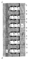
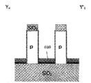
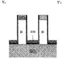
In semiconductor integrated circuit, especially use the integrated circuit of MOS transistor constantly highly integrated.Be accompanied by that this is highly integrated, wherein employed MOS transistor then miniaturization proceeds to nanometer (nano) field.The basic circuit of digital circuit is Nverter circuit (inverter circuit); If during the miniaturization of the MOS transistor of this Nverter circuit of formation; The inhibition difficulty that leakage current (1eak current) is then arranged; The reduction of the reliability that generation causes because of hot carrier effect (hot carrier effect), and because the requirement that necessary current amount is guaranteed and can't reduce the problem of the occupied area of circuit.In order to address this is that; Proposed a kind ofly source electrode (source), grid (gate), drain electrode (drain) to be disposed at vertical direction for substrate; Grid is the Surrounding Gate Transistor (SGT) (all around gate transistor) of the structure of encirclement island semiconductor layer, and the CMOS Nverter circuit (CMOS inverter circuit) (for example patent documentation 1, patent documentation 2, patent documentation 3) that proposes a kind of SGT of use.
Two sections CMOS reversers that the output of first reverser of the known SGT of demonstration use is imported into second reverser are in Fig. 1 (non-patent literature 1).And, show that profile is in Fig. 2.First reverser is to be made up of two pMOS SGT 01,02, a nMOS SGT 03.Second reverser is to be made up of two pMOS SGT 04,05, two nMOS SGT 06,07.In two sections CMOS reversers that use known SGT, be to use first power supply supply distribution Vss, second source to supply with the SGT that distribution Vcc supplies with via the diffusion layer of silicon substrate through contact terminal (contact).That is, the power line of nMOS, pMOS be disposed at the substrate that disposes nMOS, pMOS on the side of bottom of area of grid in regional different zones.The resistance of the metal wiring that the resistance of diffusion layer and power supply are supplied with is compared very big.Increase if first power supply is supplied with the resistance of distribution Vss, second source supply distribution Vcc, the source voltage that then is applied to nMOS SGT also increases than the first supply voltage Vss, and the source voltage that is applied to pMOS SGT also reduces than second source voltage vcc.If the source voltage of nMOS SGT also increases than the first supply voltage Vss, then the drive current of nMOS SGT descends.If the source voltage of pMOS SGT also reduces than second source voltage vcc, then the drive current of pMOS SGT reduces.If transistorized drive current reduces, then the speed that discharges and recharges of the electric capacity of the lead-out terminal of reverser reduces.If the speed that discharges and recharges of the electric capacity of the lead-out terminal of reverser reduces, then increase the time of delay of reverser.Therefore, carry out metal wiring through a plurality of contact terminals, apply the source electrode of first supply voltage Vss to the nMOS SGT, apply the source electrode of second source voltage vcc to pMOS SGT at diffusion layer.
And known SGT CMOS reverser is at the diffusion layer that drains contact terminal to be set, and is connected in metal wiring, is used as the output of first reverser.Be connected in the grid of the polysilicon (polysilicon) of the input of second reverser through contact terminal by the metal wiring of the output of first reverser.
That is, in using two sections CMOS reversers of known substrate ground connection type SGT, the ratio of the shared area of contact terminal is big in the circuit occupied area.And, if supplying with the resistance of distribution Vss, second source supply distribution Vcc, first power supply increases, then increase the time of delay of reverser.
And, because of the mobility (mobility) of hole (hole) mobility half the of electronics, so the wide need of the transistorized grid of pMOS are made as the wide twice of the transistorized grid of nMOS in Nverter circuit.
[patent documentation 1] japanese kokai publication hei 2-71556
[patent documentation 2] japanese kokai publication hei 2-188966
[patent documentation 3] japanese kokai publication hei 3-145761
[non-patent literature 1] S.Watanabe, K.Tsuchida, D.Takashima, Y.Oowaki, A.Nitayama; K.Hieda, H.Takato, K.Sunouchi, F.Horiguchi; K.Ohuchi, F.Masuoka, H.Hara, " A Novel Circuit Technology with Surrounding Gate Transistors (SGT ' s) for Ultra High Density DRAM ' s "; IEEE JSSC, Vol.30, No.9,1995.
Summary of the invention
(problem that invention institute desire solves)
Therefore; The object of the invention is for providing a kind of semiconductor device; Make first power supply supply with the area that distribution Vss and second source supply with distribution Vcc by use and reduce, reduce the CMOS reverser combined circuit formation at least two section or more of resistance with high integrated, the high speed of the SGT of the twice that the wide grid that is made as nMOS SGT of the grid of pMOS SGT is wide.
(means that are used to deal with problems)
In order to solve said problem, the present invention provides a kind of semiconductor device, possesses the CMOS reverser combined circuit of the CMOS reverser of combination more than at least two sections;
Said CMOS reverser combined circuit comprises a CMOS reverser and the 2nd CMOS reverser, by two sections CMOS reversers of the MOS transistor formation that on substrate, is arranged in two row (row), three row (column);
Each of first row and tertial MOS transistor is p raceway groove (channel) MOS transistor;
Each of the MOS transistor of secondary series is the n channel MOS transistor;
Each of said p channel MOS transistor and n channel MOS transistor has substrate, and drain electrode, grid, source electrode are disposed at vertical direction, and grid surrounds the structure of island semiconductor layer;
A said CMOS reverser comprises:
Two p channel MOS transistors of first row;
One side's of secondary series n channel MOS transistor;
The input terminal of the one CMOS reverser is with the mode distribution of the grid of two p channel MOS transistors of the grid of the said side's that interconnects secondary series n channel MOS transistor and first row;
The lead-out terminal of the one CMOS reverser is with the mode distribution of the drain diffusion layer of two p channel MOS transistors of the drain diffusion layer of the said side's that interconnects secondary series through the island semiconductor lower layer n channel MOS transistor and first row;
First power supply that the one CMOS reverser is used is supplied with distribution, and distribution is on the source diffusion layer of a said side's of secondary series n channel MOS transistor; And
The second source that the one CMOS reverser is used is supplied with distribution, and distribution is on the source diffusion layer of two p channel MOS transistors of first row;
Said the 2nd CMOS reverser comprises:
Tertial two p channel MOS transistors;
The opposing party's of the secondary series different n channel MOS transistor with the said side's of secondary series n channel MOS transistor;
The input terminal of the 2nd CMOS reverser is with the mode distribution of the grid of the grid of said the opposing party's of interconnecting secondary series n channel MOS transistor and tertial two p channel MOS transistors;
The lead-out terminal of the 2nd CMOS reverser is with the mode distribution of the drain diffusion layer of the drain diffusion layer of said the opposing party's of interconnecting secondary series through the island semiconductor lower layer n channel MOS transistor and tertial two p channel MOS transistors;
First power supply that the 2nd CMOS reverser is used is supplied with distribution, and distribution is on the source diffusion layer of said the opposing party's of secondary series n channel MOS transistor; And
Second source is supplied with distribution, and distribution is on the source diffusion layer of tertial two p channel MOS transistors;
It is on the source diffusion layer of the n of secondary series channel MOS transistor, to interconnect that first power supply that first power supply supply distribution that a said CMOS reverser is used and the 2nd CMOS reverser are used is supplied with distribution;
The lead-out terminal of the one CMOS reverser is the input terminal that is connected in the 2nd CMOS reverser.
In preferred mode of the present invention, a kind of semiconductor device is provided, said CMOS reverser combined circuit possesses at the CMOS reverser of arranging 2 * N section of N (N is more than 2) said two sections CMOS reversers on the substrate in line direction;
The lead-out terminal of each CMOS reverser is connected in the input terminal of the CMOS reverser that is adjacent to this lead-out terminal;
Each bar that the second source of distribution on the source diffusion layer of 4 adjoining p channel MOS transistors supplied with distribution is on the source diffusion layer, to interconnect.
In other preferred mode, a kind of semiconductor device is provided, said CMOS reverser combined circuit possesses in that the said CMOS reverser more than two sections is arranged with the CMOS reverser of M (M is more than 2) at column direction in line direction to the major general on the substrate;
On the source diffusion layer of each p channel MOS transistor, interconnect the second source that each the had supply distribution of ranking in a M said CMOS reverser of column direction;
The second source that each had that on the source diffusion layer of each p channel MOS transistor, interconnects M said the 2nd CMOS reverser that is arranged in column direction is supplied with distribution;
First power supply that each had that on the source diffusion layer of each n channel MOS transistor, interconnects a M said CMOS reverser that is arranged in column direction is supplied with distribution, is supplied with distribution with first power supply that each had of the M that is arranged in column direction said the 2nd a CMOS reverser.
And; In other preferred mode; A kind of semiconductor device is provided; Said CMOS reverser combined circuit possesses is arranging N (N is more than 2) said two sections CMOS reversers in line direction on the substrate, and arranges the CMOS reverser of M (M is more than 2) said two sections CMOS reversers in column direction;
Spread all over column direction reciprocally connects first power supply supply distribution of the CMOS reverser that is arranged in column direction continuously on the source diffusion layer of n channel MOS transistor each bar;
Spread all over column direction reciprocally connects the second source supply distribution of the CMOS reverser that is arranged in column direction continuously on the source diffusion layer of p channel MOS transistor each bar;
The second source supply distribution that is adjacent to the CMOS reverser of line direction more reciprocally connects on the source diffusion layer at the p channel MOS transistor in line direction;
The lead-out terminal of each CMOS reverser is the input terminal that is connected in the CMOS reverser that is adjacent to line direction.
In other words, the present invention is a kind of semiconductor device, possesses the CMOS reverser combined circuit of the CMOS reverser of combination more than at least two sections, is the semiconductor device that is made up of the CMOS reverser combined circuit more than at least two sections that following member constitutes:
The one CMOS reverser is the CMOS reverser that has like lower member:
The n channel semiconductor devices of the first row secondary series has for substrate drain electrode, grid, source electrode is disposed at vertical direction, and grid surrounds the structure of island semiconductor layer;
The p channel semiconductor devices of first row first row has for substrate drain electrode, grid, source electrode is disposed at vertical direction, and grid surrounds the structure of island semiconductor layer;
The p channel semiconductor devices of second row first row has for substrate drain electrode, grid, source electrode is disposed at vertical direction, and grid surrounds the structure of island semiconductor layer;
The input terminal of the one CMOS reverser, the mode distribution of the grid of the p channel semiconductor devices that is listed as with grid and first row first row and second row first of the n channel semiconductor devices that interconnects the first row secondary series;
The lead-out terminal of the one CMOS reverser, the mode distribution of the drain diffusion layer of the p channel semiconductor devices that is listed as with drain diffusion layer and first row first row and second row first of the n channel semiconductor devices that interconnects the first row secondary series through the island semiconductor lower layer;
First power supply is supplied with distribution Vss, is connected in the source diffusion layer of the n channel semiconductor devices of the first row secondary series; And
Second source is supplied with distribution Vcc, is connected in the source diffusion layer of the p channel semiconductor devices of first row, first row and second row, first row;
The 2nd CMOS reverser is the CMOS reverser that has like lower member:
The n channel semiconductor devices of the second row secondary series has for substrate drain electrode, grid, source electrode is disposed at vertical direction, and grid surrounds the structure of island semiconductor layer;
The tertial p channel semiconductor devices of first row has substrate, drain electrode, grid, source electrode are disposed at vertical direction, and grid surrounds the structure of island semiconductor layer;
The tertial p channel semiconductor devices of second row has for substrate drain electrode, grid, source electrode are disposed at vertical direction, and grid surrounds the structure of island semiconductor layer;
The input terminal of the 2nd CMOS reverser is with the grid of the n channel semiconductor devices that interconnects the second row secondary series and the mode distribution of the grid of first row the 3rd row and the second capable tertial p channel semiconductor devices;
The lead-out terminal of the 2nd CMOS reverser is with the mode distribution of drain diffusion layer with the drain diffusion layer of first row the 3rd row and the second capable tertial p channel semiconductor devices of the n channel semiconductor devices that interconnects the second row secondary series through the island semiconductor lower layer;
First power supply is supplied with distribution Vss, is connected in the source diffusion layer of the n channel semiconductor devices of the second row secondary series; And
Second source is supplied with distribution Vcc, is connected in the source diffusion layer of first row the 3rd row and the tertial p channel semiconductor devices of second row;
The lead-out terminal of the one CMOS reverser is connected in the input terminal of the 2nd CMOS reverser;
And this CMOS reverser combined circuit more than at least two sections is to be made up of following institute:
First power supply of source diffusion layer that is connected in the n channel semiconductor devices of a CMOS reverser is supplied with distribution Vss;
First power supply of source diffusion layer that is connected in the n channel semiconductor devices of the 2nd CMOS reverser is supplied with distribution Vss;
The second source of source diffusion layer that is connected in two p channel semiconductor devices of a CMOS reverser is supplied with distribution Vcc; And
The second source of source diffusion layer that is connected in two p channel semiconductor devices of the 2nd CMOS reverser is supplied with distribution Vcc.
And, be the semiconductor device that constitutes by the CMOS reverser combined circuit more than at least 4 sections that following member constitutes:
The one CMOS reverser is the CMOS reverser that has like lower member:
The n channel semiconductor devices of the first row secondary series has for substrate drain electrode, grid, source electrode is disposed at vertical direction, and grid surrounds the structure of island semiconductor layer;
The p channel semiconductor devices of first row first row has for substrate drain electrode, grid, source electrode is disposed at vertical direction, and grid surrounds the structure of island semiconductor layer;
The p channel semiconductor devices of second row first row has for substrate drain electrode, grid, source electrode is disposed at vertical direction, and grid surrounds the structure of island semiconductor layer;
The input terminal of the one CMOS reverser, the mode distribution of the grid of the p channel semiconductor devices that is listed as with grid and the first row secondary series and second row first of the n channel semiconductor devices that interconnects the first row secondary series;
The lead-out terminal of the one CMOS reverser, the mode distribution of the drain diffusion layer of the p channel semiconductor devices that is listed as with drain diffusion layer and the first row secondary series and second row first of the n channel semiconductor devices that interconnects the first row secondary series through the island semiconductor lower layer;
First power supply is supplied with distribution Vss, is connected in the source diffusion layer of the n channel semiconductor devices of the first row secondary series; And
Second source is supplied with distribution Vcc, is connected in the source diffusion layer of the p channel semiconductor devices of first row, first row and second row, first row;
The 2nd CMOS reverser is the CMOS reverser that has like lower member:
The n channel semiconductor devices of the second row secondary series has for substrate drain electrode, grid, source electrode is disposed at vertical direction, and grid surrounds the structure of island semiconductor layer;
The tertial p channel semiconductor devices of first row has for substrate drain electrode, grid, source electrode are disposed at vertical direction, and grid surrounds the structure of island semiconductor layer;
The tertial p channel semiconductor devices of second row has for substrate drain electrode, grid, source electrode are disposed at vertical direction, and grid surrounds the structure of island semiconductor layer;
The input terminal of the 2nd CMOS reverser is with the grid of the n channel semiconductor devices that interconnects the second row secondary series and the mode distribution of the grid of first row the 3rd row and the second capable tertial p channel semiconductor devices;
The lead-out terminal of the 2nd CMOS reverser is with the mode distribution of drain diffusion layer with the drain diffusion layer of first row the 3rd row and the second capable tertial p channel semiconductor devices of the n channel semiconductor devices that interconnects the second row secondary series through the island semiconductor lower layer;
First power supply is supplied with distribution Vss, is connected in the source diffusion layer of the n channel semiconductor devices of the second row secondary series; And
Second source is supplied with distribution Vcc, is connected in the source diffusion layer of first row the 3rd row and the tertial p channel semiconductor devices of second row;
The 3rd CMOS reverser is the CMOS reverser that has like lower member:
The n channel semiconductor devices of first row the 5th row has for substrate drain electrode, grid, source electrode is disposed at vertical direction, and grid surrounds the structure of island semiconductor layer;
The p channel semiconductor devices of first row the 4th row has for substrate drain electrode, grid, source electrode is disposed at vertical direction, and grid surrounds the structure of island semiconductor layer;
The p channel semiconductor devices of second row the 4th row has for substrate drain electrode, grid, source electrode is disposed at vertical direction, and grid surrounds the structure of island semiconductor layer;
The input terminal of the 3rd CMOS reverser, the mode distribution of the grid of the p channel semiconductor devices that is listed as with grid and first row the 4th row and second row the 4th of the n channel semiconductor devices that interconnects first row the 5th row;
The lead-out terminal of the 3rd CMOS reverser, the mode distribution of the drain diffusion layer of the p channel semiconductor devices that is listed as with drain diffusion layer and first row the 4th row and second row the 4th of the n channel semiconductor devices that interconnects first row the 5th row through the island semiconductor lower layer;
First power supply is supplied with distribution Vss, is connected in the source diffusion layer of the n channel semiconductor devices of first row the 5th row; And
Second source is supplied with distribution Vcc, is connected in the source diffusion layer of the p channel semiconductor devices of first row the 4th row and second row the 4th row;
The 4th CMOS reverser is the CMOS reverser that has like lower member:
The n channel semiconductor devices of second row the 5th row has for substrate drain electrode, grid, source electrode is disposed at vertical direction, and grid surrounds the structure of island semiconductor layer;
The p channel semiconductor devices of first row the 6th row has for substrate drain electrode, grid, source electrode is disposed at vertical direction, and grid surrounds the structure of island semiconductor layer;
The p channel semiconductor devices of second row the 6th row has for substrate drain electrode, grid, source electrode is disposed at vertical direction, and grid surrounds the structure of island semiconductor layer;
The input terminal of the 4th CMOS reverser, the mode distribution of the grid of the p channel semiconductor devices that is listed as with grid and first row the 6th row and second row the 6th of the n channel semiconductor devices that interconnects second row the 5th row;
The lead-out terminal of the 4th CMOS reverser, the mode distribution of the drain diffusion layer of the p channel semiconductor devices that is listed as with drain diffusion layer and first row the 6th row and second row the 6th of the n channel semiconductor devices that interconnects second row the 5th row through the island semiconductor lower layer;
First power supply is supplied with distribution Vss, is connected in the source diffusion layer of the n channel semiconductor devices of second row the 5th row; And
Second source is supplied with distribution Vcc, is connected in the source diffusion layer of the p channel semiconductor devices of first row the 6th row and second row the 6th row;
The lead-out terminal of the one CMOS reverser is connected in the input terminal of the 2nd CMOS reverser;
The lead-out terminal of the 2nd CMOS reverser is connected in the input terminal of the 3rd CMOS reverser;
The lead-out terminal of the 3rd CMOS reverser is connected in the input terminal of the 4th CMOS reverser;
And this CMOS reverser combined circuit more than at least 4 sections is to be made up of following institute:
First power supply of source diffusion layer that is connected in the n channel semiconductor devices of a CMOS reverser is supplied with distribution Vss;
First power supply of source diffusion layer that is connected in the n channel semiconductor devices of the 2nd CMOS reverser is supplied with distribution Vss;
First power supply of source diffusion layer that is connected in the n channel semiconductor devices of the 3rd CMOS reverser is supplied with distribution Vss;
First power supply of source diffusion layer that is connected in the n channel semiconductor devices of the 4th CMOS reverser is supplied with distribution Vss;
The second source of source diffusion layer that is connected in two p channel semiconductor devices of a CMOS reverser is supplied with distribution Vcc;
The second source of source diffusion layer that is connected in two p channel semiconductor devices of the 2nd CMOS reverser is supplied with distribution Vcc;
The second source of source diffusion layer that is connected in two p channel semiconductor devices of the 3rd CMOS reverser is supplied with distribution Vcc;
The second source of source diffusion layer that is connected in two p channel semiconductor devices of the 4th CMOS reverser is supplied with distribution Vcc.
And in preferred mode of the present invention, a kind of n channel semiconductor devices (being the n channel MOS transistor) is in said semiconductor device, to be used, and this n channel MOS transistor is to constitute in the following manner:
Have for substrate drain electrode, grid, source electrode are disposed at vertical direction, and grid surrounds the structure of island semiconductor layer;
Be formed with insulating film layer up and down at grid;
Through the island semiconductor lower layer, the polysilicon distribution surrounds the part of drain diffusion layer;
Have drain diffusion layer, polysilicon distribution, grid, source diffusion layer by the structure of self-aligned metal silicate (salicide) change;
On the source diffusion layer, be formed with metal wiring.
And in other preferred mode of the present invention, a kind of p channel semiconductor devices (being the p channel MOS transistor) is in said semiconductor device, to be used, and this p channel MOS transistor is to constitute in the following manner:
Have for substrate drain electrode, grid, source electrode are disposed at vertical direction, and grid surrounds the structure of island semiconductor layer;
Be formed with insulating film layer up and down at grid;
Through the island semiconductor lower layer, the polysilicon distribution surrounds the part of drain diffusion layer;
Have drain diffusion layer, polysilicon distribution, grid, source diffusion layer by the structure of self-aligned metal silicateization;
On the source diffusion layer, be formed with metal wiring.
(invention effect)
In two sections CMOS reversers that use known SGT, use the first supply voltage Vss and second source voltage vcc to be supplied to the SGT of the diffusion layer of silicon substrate via contact terminal.That is, the power supply of nMOS SGT, pMOS SGT supply with distribution be disposed at the substrate that disposes nMOS, pMOS on the side of bottom of area of grid in regional different zones.
With respect to this, first power supply of being supplied with by nMOS SGT, pMOS SGT two sides' top is supplied with distribution Vss and second source is supplied with distribution Vcc because of having in the present invention, and possesses following member:
First power supply is supplied with distribution Vss, is connected in the source diffusion layer of the n channel semiconductor devices of first reverser;
First power supply is supplied with distribution Vss, is connected in the source diffusion layer of the n channel semiconductor devices of second reverser;
Second source is supplied with distribution Vcc, is connected in the source diffusion layer of two p channel semiconductor devices of first reverser; And
Second source is supplied with distribution Vcc, is connected in the source diffusion layer of two p channel semiconductor devices of second reverser;
Reduce so first power supply is supplied with the area of distribution Vss and second source supply distribution Vcc, can obtain the semiconductor device that constitutes by the high integrated CMOS reverser combined circuit that uses SGT.
And first power supply of being supplied with by nMOS SGT, pMOS SGT two sides' top is supplied with distribution Vss, second source is supplied with distribution Vcc because of having, and possesses following member:
First power supply is supplied with distribution Vss, is connected in the source diffusion layer of the n channel semiconductor devices of first reverser;
First power supply is supplied with distribution Vss, is connected in the source diffusion layer of the n channel semiconductor devices of second reverser;
Second source is supplied with distribution Vcc, is connected in the source diffusion layer of two p channel semiconductor devices of first reverser; And
Second source is supplied with distribution Vcc, is connected in the source diffusion layer of two p channel semiconductor devices of second reverser;
Reduce so first power supply is supplied with the resistance that distribution Vss and second source supply with distribution Vcc, can obtain the semiconductor device that the CMOS reverser combined circuit by the high speed of use SGT constitutes.
Because of having the lead-out terminal distribution of drain diffusion layer distribution that interconnects drain diffusion layer and the p channel semiconductor devices of n channel semiconductor devices through the island semiconductor lower layer, so member that need not be following:
The contact terminal that uses in order to the drain diffusion layer that connects the n channel semiconductor devices and metal wiring;
The contact terminal that uses in order to the drain diffusion layer that connects the p channel semiconductor devices and metal wiring; And
In order to connect the metal wiring of each contact terminal;
Can obtain the semiconductor device that constitutes by the high integrated CMOS reverser combined circuit that uses SGT.
And; Because of the pMOS SGT with first reverser is disposed at first row, first row and second row, first row; NMOS SGT is disposed at the first row secondary series; The pMOS SGT of second reverser is disposed at first row the 3rd row and second row the 3rd row, nMOS SGT is disposed at the second row secondary series, so can obtain the semiconductor device that the high integrated CMOS reverser combined circuit by use SGT constitutes.
Description of drawings
Fig. 1 (a) reaches layout and the equivalent electric circuit that (b) is to use two sections CMOS reversers of known SGT.
Fig. 2 (a) to (c) is to use the layout and the profile of two sections CMOS reversers of known SGT.
Fig. 3 is the layout of the semiconductor device relevant with the present invention.
Fig. 4 is the profile of X1-X ' 1 profile among Fig. 3 of the corresponding semiconductor device relevant with the present invention.
Fig. 5 is the profile of X2-X ' 2 profiles among Fig. 3 of the corresponding semiconductor device relevant with the present invention.
Fig. 6 is the profile of Y1-Y ' 1 profile among Fig. 3 of the corresponding semiconductor device relevant with the present invention.
Fig. 7 is the profile of Y2-Y ' 2 profiles among Fig. 3 of the corresponding semiconductor device relevant with the present invention.
Fig. 8 is the layout of the semiconductor device relevant with the present invention.
Fig. 9 is the profile of X1-X ' 1 profile among Fig. 8 of the corresponding semiconductor device relevant with the present invention.
Figure 10 is the profile of X2-X ' 2 profiles among Fig. 8 of the corresponding semiconductor device relevant with the present invention.
Figure 11 is the profile of X3-X ' 3 profiles among Fig. 8 of the corresponding semiconductor device relevant with the present invention.
Figure 12 is the profile of X4-X ' 4 profiles among Fig. 8 of the corresponding semiconductor device relevant with the present invention.
Figure 13 is the profile of X5-X ' 5 profiles among Fig. 8 of the corresponding semiconductor device relevant with the present invention.
Figure 14 is the profile of X6-X ' 6 profiles among Fig. 8 of the corresponding semiconductor device relevant with the present invention.
Figure 15 is the profile of Y1-Y ' 1 profile among Fig. 8 of the corresponding semiconductor device relevant with the present invention.
Figure 16 is the profile of Y2-Y ' 2 profiles among Fig. 8 of the corresponding semiconductor device relevant with the present invention.
Figure 17 is X1-X ' the 1 section artwork that shows the manufacturing example of the semiconductor device relevant with the present invention.
Figure 18 is X2-X ' the 2 section artworks that show the manufacturing example of the semiconductor device relevant with the present invention.
Figure 19 is Y1-Y ' the 1 section artwork that shows the manufacturing example of the semiconductor device relevant with the present invention.
Figure 20 is Y2-Y ' the 2 section artworks that show the manufacturing example of the semiconductor device relevant with the present invention.
Figure 21 is X1-X ' the 1 section artwork that shows the manufacturing example of the semiconductor device relevant with the present invention.
Figure 22 is X2-X ' the 2 section artworks that show the manufacturing example of the semiconductor device relevant with the present invention.
Figure 23 is Y1-Y ' the 1 section artwork that shows the manufacturing example of the semiconductor device relevant with the present invention.
Figure 24 is Y2-Y ' the 2 section artworks that show the manufacturing example of the semiconductor device relevant with the present invention.
Figure 25 is X1-X ' the 1 section artwork that shows the manufacturing example of the semiconductor device relevant with the present invention.
Figure 26 is X2-X ' the 2 section artworks that show the manufacturing example of the semiconductor device relevant with the present invention.
Figure 27 is Y1-Y ' the 1 section artwork that shows the manufacturing example of the semiconductor device relevant with the present invention.
Figure 28 is Y2-Y ' the 2 section artworks that show the manufacturing example of the semiconductor device relevant with the present invention.
Figure 29 is X1-X ' the 1 section artwork that shows the manufacturing example of the semiconductor device relevant with the present invention.
Figure 30 is X2-X ' the 2 section artworks that show the manufacturing example of the semiconductor device relevant with the present invention.
Figure 31 is Y1-Y ' the 1 section artwork that shows the manufacturing example of the semiconductor device relevant with the present invention.
Figure 32 is Y2-Y ' the 2 section artworks that show the manufacturing example of the semiconductor device relevant with the present invention.
Figure 33 is X1-X ' the 1 section artwork that shows the manufacturing example of the semiconductor device relevant with the present invention.
Figure 34 is X2-X ' the 2 section artworks that show the manufacturing example of the semiconductor device relevant with the present invention.
Figure 35 is Y1-Y ' the 1 section artwork that shows the manufacturing example of the semiconductor device relevant with the present invention.
Figure 36 is Y2-Y ' the 2 section artworks that show the manufacturing example of the semiconductor device relevant with the present invention.
Figure 37 is X1-X ' the 1 section artwork that shows the manufacturing example of the semiconductor device relevant with the present invention.
Figure 38 is X2-X ' the 2 section artworks that show the manufacturing example of the semiconductor device relevant with the present invention.
Figure 39 is Y1-Y ' the 1 section artwork that shows the manufacturing example of the semiconductor device relevant with the present invention.
Figure 40 is Y2-Y ' the 2 section artworks that show the manufacturing example of the semiconductor device relevant with the present invention.
Figure 41 is X1-X ' the 1 section artwork that shows the manufacturing example of the semiconductor device relevant with the present invention.
Figure 42 is X2-X ' the 2 section artworks that show the manufacturing example of the semiconductor device relevant with the present invention.
Figure 43 is Y1-Y ' the 1 section artwork that shows the manufacturing example of the semiconductor device relevant with the present invention.
Figure 44 is Y2-Y ' the 2 section artworks that show the manufacturing example of the semiconductor device relevant with the present invention.
Figure 45 is X1-X ' the 1 section artwork that shows the manufacturing example of the semiconductor device relevant with the present invention.
Figure 46 is X2-X ' the 2 section artworks that show the manufacturing example of the semiconductor device relevant with the present invention.
Figure 47 is Y1-Y ' the 1 section artwork that shows the manufacturing example of the semiconductor device relevant with the present invention.
Figure 48 is Y2-Y ' the 2 section artworks that show the manufacturing example of the semiconductor device relevant with the present invention.
Figure 49 is X1-X ' the 1 section artwork that shows the manufacturing example of the semiconductor device relevant with the present invention.
Figure 50 is X2-X ' the 2 section artworks that show the manufacturing example of the semiconductor device relevant with the present invention.
Figure 51 is Y1-Y ' the 1 section artwork that shows the manufacturing example of the semiconductor device relevant with the present invention.
Figure 52 is Y2-Y ' the 2 section artworks that show the manufacturing example of the semiconductor device relevant with the present invention.
Figure 53 is X1-X ' the 1 section artwork that shows the manufacturing example of the semiconductor device relevant with the present invention.
Figure 54 is X2-X ' the 2 section artworks that show the manufacturing example of the semiconductor device relevant with the present invention.
Figure 55 is Y1-Y ' the 1 section artwork that shows the manufacturing example of the semiconductor device relevant with the present invention.
Figure 56 is Y2-Y ' the 2 section artworks that show the manufacturing example of the semiconductor device relevant with the present invention.
Figure 57 is X1-X ' the 1 section artwork that shows the manufacturing example of the semiconductor device relevant with the present invention.
Figure 58 is X2-X ' the 2 section artworks that show the manufacturing example of the semiconductor device relevant with the present invention.
Figure 59 is Y1-Y ' the 1 section artwork that shows the manufacturing example of the semiconductor device relevant with the present invention.
Figure 60 is Y2-Y ' the 2 section artworks that show the manufacturing example of the semiconductor device relevant with the present invention.
Figure 61 is X1-X ' the 1 section artwork that shows the manufacturing example of the semiconductor device relevant with the present invention.
Figure 62 is X2-X ' the 2 section artworks that show the manufacturing example of the semiconductor device relevant with the present invention.
Figure 63 is Y1-Y ' the 1 section artwork that shows the manufacturing example of the semiconductor device relevant with the present invention.
Figure 64 is Y2-Y ' the 2 section artworks that show the manufacturing example of the semiconductor device relevant with the present invention.
Figure 65 is X1-X ' the 1 section artwork that shows the manufacturing example of the semiconductor device relevant with the present invention.
Figure 66 is X2-X ' the 2 section artworks that show the manufacturing example of the semiconductor device relevant with the present invention.
Figure 67 is Y1-Y ' the 1 section artwork that shows the manufacturing example of the semiconductor device relevant with the present invention.
Figure 68 is Y2-Y ' the 2 section artworks that show the manufacturing example of the semiconductor device relevant with the present invention.
Figure 69 is X1-X ' the 1 section artwork that shows the manufacturing example of the semiconductor device relevant with the present invention.
Figure 70 is X2-X ' the 2 section artworks that show the manufacturing example of the semiconductor device relevant with the present invention.
Figure 71 is Y1-Y ' the 1 section artwork that shows the manufacturing example of the semiconductor device relevant with the present invention.
Figure 72 is Y2-Y ' the 2 section artworks that show the manufacturing example of the semiconductor device relevant with the present invention.
Figure 73 is X1-X ' the 1 section artwork that shows the manufacturing example of the semiconductor device relevant with the present invention.
Figure 74 is X2-X ' the 2 section artworks that show the manufacturing example of the semiconductor device relevant with the present invention.
Figure 75 is Y1-Y ' the 1 section artwork that shows the manufacturing example of the semiconductor device relevant with the present invention.
Figure 76 is Y2-Y ' the 2 section artworks that show the manufacturing example of the semiconductor device relevant with the present invention.
Figure 77 is X1-X ' the 1 section artwork that shows the manufacturing example of the semiconductor device relevant with the present invention.
Figure 78 is X2-X ' the 2 section artworks that show the manufacturing example of the semiconductor device relevant with the present invention.
Figure 79 is Y1-Y ' the 1 section artwork that shows the manufacturing example of the semiconductor device relevant with the present invention.
Figure 80 is Y2-Y ' the 2 section artworks that show the manufacturing example of the semiconductor device relevant with the present invention.
Figure 81 is X1-X ' the 1 section artwork that shows the manufacturing example of the semiconductor device relevant with the present invention.
Figure 82 is X2-X ' the 2 section artworks that show the manufacturing example of the semiconductor device relevant with the present invention.
Figure 83 is Y1-Y ' the 1 section artwork that shows the manufacturing example of the semiconductor device relevant with the present invention.
Figure 84 is Y2-Y ' the 2 section artworks that show the manufacturing example of the semiconductor device relevant with the present invention.
Figure 85 is X1-X ' the 1 section artwork that shows the manufacturing example of the semiconductor device relevant with the present invention.
Figure 86 is X2-X ' the 2 section artworks that show the manufacturing example of the semiconductor device relevant with the present invention.
Figure 87 is Y1-Y ' the 1 section artwork that shows the manufacturing example of the semiconductor device relevant with the present invention.
Figure 88 is Y2-Y ' the 2 section artworks that show the manufacturing example of the semiconductor device relevant with the present invention.
Figure 89 is X1-X ' the 1 section artwork that shows the manufacturing example of the semiconductor device relevant with the present invention.
Figure 90 is X2-X ' the 2 section artworks that show the manufacturing example of the semiconductor device relevant with the present invention.
Figure 91 is Y1-Y ' the 1 section artwork that shows the manufacturing example of the semiconductor device relevant with the present invention.
Figure 92 is Y2-Y ' the 2 section artworks that show the manufacturing example of the semiconductor device relevant with the present invention.
Figure 93 is X1-X ' the 1 section artwork that shows the manufacturing example of the semiconductor device relevant with the present invention.
Figure 94 is X2-X ' the 2 section artworks that show the manufacturing example of the semiconductor device relevant with the present invention.
Figure 95 is Y1-Y ' the 1 section artwork that shows the manufacturing example of the semiconductor device relevant with the present invention.
Figure 96 is Y2-Y ' the 2 section artworks that show the manufacturing example of the semiconductor device relevant with the present invention.
Figure 97 is X1-X ' the 1 section artwork that shows the manufacturing example of the semiconductor device relevant with the present invention.
Figure 98 is X2-X ' the 2 section artworks that show the manufacturing example of the semiconductor device relevant with the present invention.
Figure 99 is Y1-Y ' the 1 section artwork that shows the manufacturing example of the semiconductor device relevant with the present invention.
Figure 100 is Y2-Y ' the 2 section artworks that show the manufacturing example of the semiconductor device relevant with the present invention.
Figure 101 is X1-X ' the 1 section artwork that shows the manufacturing example of the semiconductor device relevant with the present invention.
Figure 102 is X2-X ' the 2 section artworks that show the manufacturing example of the semiconductor device relevant with the present invention.
Figure 103 is Y1-Y ' the 1 section artwork that shows the manufacturing example of the semiconductor device relevant with the present invention.
Figure 104 is Y2-Y ' the 2 section artworks that show the manufacturing example of the semiconductor device relevant with the present invention.
Figure 105 is X1-X ' the 1 section artwork that shows the manufacturing example of the semiconductor device relevant with the present invention.
Figure 106 is X2-X ' the 2 section artworks that show the manufacturing example of the semiconductor device relevant with the present invention.
Figure 107 is Y1-Y ' the 1 section artwork that shows the manufacturing example of the semiconductor device relevant with the present invention.
Figure 108 is Y2-Y ' the 2 section artworks that show the manufacturing example of the semiconductor device relevant with the present invention.
Figure 109 is X1-X ' the 1 section artwork that shows the manufacturing example of the semiconductor device relevant with the present invention.
Figure 110 is X2-X ' the 2 section artworks that show the manufacturing example of the semiconductor device relevant with the present invention.
Figure 111 is Y1-Y ' the 1 section artwork that shows the manufacturing example of the semiconductor device relevant with the present invention.
Figure 112 is Y2-Y ' the 2 section artworks that show the manufacturing example of the semiconductor device relevant with the present invention.
Figure 113 is X1-X ' the 1 section artwork that shows the manufacturing example of the semiconductor device relevant with the present invention.
Figure 114 is X2-X ' the 2 section artworks that show the manufacturing example of the semiconductor device relevant with the present invention.
Figure 115 is Y1-Y ' the 1 section artwork that shows the manufacturing example of the semiconductor device relevant with the present invention.
Figure 116 is Y2-Y ' the 2 section artworks that show the manufacturing example of the semiconductor device relevant with the present invention.
Figure 117 is X1-X ' the 1 section artwork that shows the manufacturing example of the semiconductor device relevant with the present invention.
Figure 118 is X2-X ' the 2 section artworks that show the manufacturing example of the semiconductor device relevant with the present invention.
Figure 119 is Y1-Y ' the 1 section artwork that shows the manufacturing example of the semiconductor device relevant with the present invention.
Figure 120 is Y2-Y ' the 2 section artworks that show the manufacturing example of the semiconductor device relevant with the present invention.
Figure 121 is X1-X ' the 1 section artwork that shows the manufacturing example of the semiconductor device relevant with the present invention.
Figure 122 is X2-X ' the 2 section artworks that show the manufacturing example of the semiconductor device relevant with the present invention.
Figure 123 is Y1-Y ' the 1 section artwork that shows the manufacturing example of the semiconductor device relevant with the present invention.
Figure 124 is Y2-Y ' the 2 section artworks that show the manufacturing example of the semiconductor device relevant with the present invention.
Figure 125 is X1-X ' the 1 section artwork that shows the manufacturing example of the semiconductor device relevant with the present invention.
Figure 126 is X2-X ' the 2 section artworks that show the manufacturing example of the semiconductor device relevant with the present invention.
Figure 127 is Y1-Y ' the 1 section artwork that shows the manufacturing example of the semiconductor device relevant with the present invention.
Figure 128 is Y2-Y ' the 2 section artworks that show the manufacturing example of the semiconductor device relevant with the present invention.
Figure 129 is X1-X ' the 1 section artwork that shows the manufacturing example of the semiconductor device relevant with the present invention.
Figure 130 is X2-X ' the 2 section artworks that show the manufacturing example of the semiconductor device relevant with the present invention.
Figure 131 is Y1-Y ' the 1 section artwork that shows the manufacturing example of the semiconductor device relevant with the present invention.
Figure 132 is Y2-Y ' the 2 section artworks that show the manufacturing example of the semiconductor device relevant with the present invention.
Figure 133 is X1-X ' the 1 section artwork that shows the manufacturing example of the semiconductor device relevant with the present invention.
Figure 134 is X2-X ' the 2 section artworks that show the manufacturing example of the semiconductor device relevant with the present invention.
Figure 135 is Y1-Y ' the 1 section artwork that shows the manufacturing example of the semiconductor device relevant with the present invention.
Figure 136 is Y2-Y ' the 2 section artworks that show the manufacturing example of the semiconductor device relevant with the present invention.
Figure 137 is X1-X ' the 1 section artwork that shows the manufacturing example of the semiconductor device relevant with the present invention.
Figure 138 is X2-X ' the 2 section artworks that show the manufacturing example of the semiconductor device relevant with the present invention.
Figure 139 is Y1-Y ' the 1 section artwork that shows the manufacturing example of the semiconductor device relevant with the present invention.
Figure 140 is Y2-Y ' the 2 section artworks that show the manufacturing example of the semiconductor device relevant with the present invention.
Figure 141 is X1-X ' the 1 section artwork that shows the manufacturing example of the semiconductor device relevant with the present invention.
Figure 142 is X2-X ' the 2 section artworks that show the manufacturing example of the semiconductor device relevant with the present invention.
Figure 143 is Y1-Y ' the 1 section artwork that shows the manufacturing example of the semiconductor device relevant with the present invention.
Figure 144 is Y2-Y ' the 2 section artworks that show the manufacturing example of the semiconductor device relevant with the present invention.
Figure 145 is X1-X ' the 1 section artwork that shows the manufacturing example of the semiconductor device relevant with the present invention.
Figure 146 is X2-X ' the 2 section artworks that show the manufacturing example of the semiconductor device relevant with the present invention.
Figure 147 is Y1-Y ' the 1 section artwork that shows the manufacturing example of the semiconductor device relevant with the present invention.
Figure 148 is Y2-Y ' the 2 section artworks that show the manufacturing example of the semiconductor device relevant with the present invention.
Figure 149 is X1-X ' the 1 section artwork that shows the manufacturing example of the semiconductor device relevant with the present invention.
Figure 150 is X2-X ' the 2 section artworks that show the manufacturing example of the semiconductor device relevant with the present invention.
Figure 151 is Y1-Y ' the 1 section artwork that shows the manufacturing example of the semiconductor device relevant with the present invention.
Figure 152 is Y2-Y ' the 2 section artworks that show the manufacturing example of the semiconductor device relevant with the present invention.
Figure 153 is X1-X ' the 1 section artwork that shows the manufacturing example of the semiconductor device relevant with the present invention.
Figure 154 is X2-X ' the 2 section artworks that show the manufacturing example of the semiconductor device relevant with the present invention.
Figure 155 is Y1-Y ' the 1 section artwork that shows the manufacturing example of the semiconductor device relevant with the present invention.
Figure 156 is Y2-Y ' the 2 section artworks that show the manufacturing example of the semiconductor device relevant with the present invention.
Figure 157 is X1-X ' the 1 section artwork that shows the manufacturing example of the semiconductor device relevant with the present invention.
Figure 158 is X2-X ' the 2 section artworks that show the manufacturing example of the semiconductor device relevant with the present invention.
Figure 159 is Y1-Y ' the 1 section artwork that shows the manufacturing example of the semiconductor device relevant with the present invention.
Figure 160 is Y2-Y ' the 2 section artworks that show the manufacturing example of the semiconductor device relevant with the present invention.
Figure 161 is X1-X ' the 1 section artwork that shows the manufacturing example of the semiconductor device relevant with the present invention.
Figure 162 is X2-X ' the 2 section artworks that show the manufacturing example of the semiconductor device relevant with the present invention.
Figure 163 is Y1-Y ' the 1 section artwork that shows the manufacturing example of the semiconductor device relevant with the present invention.
Figure 164 is Y2-Y ' the 2 section artworks that show the manufacturing example of the semiconductor device relevant with the present invention.
Figure 165 is X1-X ' the 1 section artwork that shows the manufacturing example of the semiconductor device relevant with the present invention.
Figure 166 is X2-X ' the 2 section artworks that show the manufacturing example of the semiconductor device relevant with the present invention.
Figure 167 is Y1-Y ' the 1 section artwork that shows the manufacturing example of the semiconductor device relevant with the present invention.
Figure 168 is Y2-Y ' the 2 section artworks that show the manufacturing example of the semiconductor device relevant with the present invention.
Figure 169 is X1-X ' the 1 section artwork that shows the manufacturing example of the semiconductor device relevant with the present invention.
Figure 170 is X2-X ' the 2 section artworks that show the manufacturing example of the semiconductor device relevant with the present invention.
Figure 171 is Y1-Y ' the 1 section artwork that shows the manufacturing example of the semiconductor device relevant with the present invention.
Figure 172 is Y2-Y ' the 2 section artworks that show the manufacturing example of the semiconductor device relevant with the present invention.
Figure 173 is X1-X ' the 1 section artwork that shows the manufacturing example of the semiconductor device relevant with the present invention.
Figure 174 is X2-X ' the 2 section artworks that show the manufacturing example of the semiconductor device relevant with the present invention.
Figure 175 is Y1-Y ' the 1 section artwork that shows the manufacturing example of the semiconductor device relevant with the present invention.
Figure 176 is Y2-Y ' the 2 section artworks that show the manufacturing example of the semiconductor device relevant with the present invention.
Figure 177 is X1-X ' the 1 section artwork that shows the manufacturing example of the semiconductor device relevant with the present invention.
Figure 178 is X2-X ' the 2 section artworks that show the manufacturing example of the semiconductor device relevant with the present invention.
Figure 179 is Y1-Y ' the 1 section artwork that shows the manufacturing example of the semiconductor device relevant with the present invention.
Figure 180 is Y2-Y ' the 2 section artworks that show the manufacturing example of the semiconductor device relevant with the present invention.
Figure 181 is X1-X ' the 1 section artwork that shows the manufacturing example of the semiconductor device relevant with the present invention.
Figure 182 is X2-X ' the 2 section artworks that show the manufacturing example of the semiconductor device relevant with the present invention.
Figure 183 is Y1-Y ' the 1 section artwork that shows the manufacturing example of the semiconductor device relevant with the present invention.
Figure 184 is Y2-Y ' the 2 section artworks that show the manufacturing example of the semiconductor device relevant with the present invention.
Figure 185 is X1-X ' the 1 section artwork that shows the manufacturing example of the semiconductor device relevant with the present invention.
Figure 186 is X2-X ' the 2 section artworks that show the manufacturing example of the semiconductor device relevant with the present invention.
Figure 187 is Y1-Y ' the 1 section artwork that shows the manufacturing example of the semiconductor device relevant with the present invention.
Figure 188 is Y2-Y ' the 2 section artworks that show the manufacturing example of the semiconductor device relevant with the present invention.
Figure 189 is X1-X ' the 1 section artwork that shows the manufacturing example of the semiconductor device relevant with the present invention.
Figure 190 is X2-X ' the 2 section artworks that show the manufacturing example of the semiconductor device relevant with the present invention.
Figure 191 is Y1-Y ' the 1 section artwork that shows the manufacturing example of the semiconductor device relevant with the present invention.
Figure 192 is Y2-Y ' the 2 section artworks that show the manufacturing example of the semiconductor device relevant with the present invention.
Figure 193 is X1-X ' the 1 section artwork that shows the manufacturing example of the semiconductor device relevant with the present invention.
Figure 194 is X2-X ' the 2 section artworks that show the manufacturing example of the semiconductor device relevant with the present invention.
Figure 195 is Y1-Y ' the 1 section artwork that shows the manufacturing example of the semiconductor device relevant with the present invention.
Figure 196 is Y2-Y ' the 2 section artworks that show the manufacturing example of the semiconductor device relevant with the present invention.
Figure 197 is X1-X ' the 1 section artwork that shows the manufacturing example of the semiconductor device relevant with the present invention.
Figure 198 is X2-X ' the 2 section artworks that show the manufacturing example of the semiconductor device relevant with the present invention.
Figure 199 is Y1-Y ' the 1 section artwork that shows the manufacturing example of the semiconductor device relevant with the present invention.
Figure 200 is Y2-Y ' the 2 section artworks that show the manufacturing example of the semiconductor device relevant with the present invention.
Figure 20 1 is X1-X ' the 1 section artwork that shows the manufacturing example of the semiconductor device relevant with the present invention.
Figure 20 2 is X2-X ' the 2 section artworks that show the manufacturing example of the semiconductor device relevant with the present invention.
Figure 20 3 is Y1-Y ' the 1 section artworks that show the manufacturing example of the semiconductor device relevant with the present invention.
Figure 20 4 is Y2-Y ' the 2 section artworks that show the manufacturing example of the semiconductor device relevant with the present invention.
Figure 20 5 is X1-X ' the 1 section artworks that show the manufacturing example of the semiconductor device relevant with the present invention.
Figure 20 6 is X2-X ' the 2 section artworks that show the manufacturing example of the semiconductor device relevant with the present invention.
Figure 20 7 is Y1-Y ' the 1 section artworks that show the manufacturing example of the semiconductor device relevant with the present invention.
Figure 20 8 is Y2-Y ' the 2 section artworks that show the manufacturing example of the semiconductor device relevant with the present invention.
Figure 20 9 is X1-X ' the 1 section artworks that show the manufacturing example of the semiconductor device relevant with the present invention.
Figure 21 0 is X2-X ' the 2 section artworks that show the manufacturing example of the semiconductor device relevant with the present invention.
Figure 21 1 is Y1-Y ' the 1 section artwork that shows the manufacturing example of the semiconductor device relevant with the present invention.
Figure 21 2 is Y2-Y ' the 2 section artworks that show the manufacturing example of the semiconductor device relevant with the present invention.
Description of reference numerals in the above-mentioned accompanying drawing is following:
1、2、4、5pMOS?SGT 3、6、7nMOS?SGT
8,108 silicon oxide films
9,13,16,20,24,27,31,35,38,42,46,49,109,113,116,120,124,127,131,135,138,142,146,149,209,213,216,220,224,227,231,235,238,242,246,249,309,313,316,320,324,327,331,335,338,342,346,349 drain diffusion layer
10,14,17,21,25,28,32,36,39,43,47,50,110,114,117,121,125,128,132,136,139,143,147,150,210,214,217,221,225,228,232,236,239,243,247,250,310,314,317,321,325,328,332,336,339,343,347,350 island semiconductor layers
11,15,18,22,26,29,33,37,40,44,48,51,111,115,118,122,126,129,133,137,140,144,148,151,211,215,218,222,226,229,233,237,240,244,248,251,311,315,318,322,326,329,333,337,340,344,348,351 source diffusion layers
12,23,34,45,112,123,134,145,212,223,234,245,312,323,334,345 grids
19, the lead-out terminal distribution of 30,41,52,119,130,141,152,219,230,241,252,319,330,341,352 island semiconductor lower layers
53,54,55,153,154,155,253,254,255,353,354,355 contact terminals
56,58,60,156,158,160 second sources are supplied with distribution Vcc
57,59,157,159 first power supplys are supplied with distribution Vss
500 silicon
501,538,558,569,577 oxide-films
502,503,504,509,510,534,535,536,537,554,555,556,557,559,563,564,565,566,567,570,572,573,574,575,576 photoresists
505,506,507,508 p type silicon
511,512,513,514,515,516,517,518 n type silicon
519,539,553 nitride films
520,533,552 polysilicons
521,522,523,524,525,526,527,528,529,530,531,532 side wall spacer
540,541,542,543,544,545,546,547,548,549,550,551 grid oxidation films
560,561,562 contact holes, 568,571 metals
Embodiment
Below, record and narrate the present invention according to embodiment shown in the drawings.In addition, the present invention is not limited by this embodiment.
The layout (layout) and the profile construction that show the semiconductor device relevant with the present invention respectively are in Fig. 3, Fig. 4, Fig. 5, Fig. 6, Fig. 7.
In the present embodiment; On silicon oxide film 8, be formed with the lead-out terminal distribution 19 and drain diffusion layer 9 of island semiconductor lower layer; Be formed with island semiconductor layer 10 above that; Be formed with source diffusion layer 11 on the top of this island semiconductor layer 10, on the channel region of the sidewall that is clipped by drain diffusion layer and source diffusion layer, be formed with the grid 12 that forms across gate insulating film, form the n channel semiconductor devices (n channel MOS transistor) of first row (row) secondary series (column).
And; On silicon oxide film 8, be formed with island semiconductor bottom distribution 19, drain diffusion layer 13; Be formed with island semiconductor layer 14 above that; Be formed with source diffusion layer 15 on the top of this island semiconductor layer 14, on the channel region of the sidewall that is clipped by drain diffusion layer and source diffusion layer, be formed with the grid 12 that forms across gate insulating film, form the p channel semiconductor devices (p channel MOS transistor) of first row, first row.And; On silicon oxide film 8, be formed with island semiconductor bottom distribution 19 and drain diffusion layer 16; Be formed with island semiconductor layer 17 above that; Be formed with source diffusion layer 18 on the top of this island semiconductor layer 17, on the channel region of the sidewall that is clipped by drain diffusion layer and source diffusion layer, be formed with the grid 12 that forms across gate insulating film, form the p channel semiconductor devices of second row, first row.
Be formed with first reverser through said two p channel semiconductor devices and a n channel semiconductor devices.
And; On silicon oxide film 8, be formed with the lead-out terminal distribution 30 and drain diffusion layer 20 of island semiconductor lower layer; Be formed with island semiconductor layer 21 above that; Be formed with source diffusion layer 22 on the top of this island semiconductor layer 21, on the channel region of the sidewall that is clipped by drain diffusion layer and source diffusion layer, be formed with the grid 23 that forms across gate insulating film, form the n channel semiconductor devices of the second row secondary series.
And; On silicon oxide film 8, be formed with island semiconductor bottom distribution 30 and drain diffusion layer 27; Be formed with island semiconductor layer 28 above that; Be formed with source diffusion layer 29 on the top of this island semiconductor layer 28, on the channel region of the sidewall that is clipped by drain diffusion layer and source diffusion layer, be formed with the grid 23 that forms across gate insulating film, form the tertial p channel semiconductor devices of first row.And; On silicon oxide film 8, be formed with island semiconductor bottom distribution 30 and drain diffusion layer 24; Be formed with island semiconductor layer 25 above that; Be formed with source diffusion layer 26 on the top of this island semiconductor layer 25, on the channel region of the sidewall that is clipped by drain diffusion layer and source diffusion layer, be formed with the grid 23 that forms across gate insulating film, form the tertial p channel semiconductor devices of second row.
Be formed with second reverser through said two p channel semiconductor devices and a n channel semiconductor devices.
And; On silicon oxide film 8, be formed with the lead-out terminal distribution 41 and drain diffusion layer 31 of island semiconductor lower layer; Be formed with island semiconductor layer 32 above that; Be formed with source diffusion layer 33 on the top of this island semiconductor layer 32, on the channel region of the sidewall that is clipped by drain diffusion layer and source diffusion layer, be formed with the grid 34 that forms across gate insulating film, form the n channel semiconductor devices of first row the 5th row.
And; On silicon oxide film 8, be formed with island semiconductor bottom distribution 41 and drain diffusion layer 38; Be formed with island semiconductor layer 39 above that; Be formed with source diffusion layer 40 on the top of this island semiconductor layer 39, on the channel region of the sidewall that is clipped by drain diffusion layer and source diffusion layer, be formed with the grid 34 that forms across gate insulating film, form the p channel semiconductor devices of first row the 4th row.And; On silicon oxide film 8, be formed with island semiconductor bottom distribution 41 and drain diffusion layer 35; Be formed with island semiconductor layer 36 above that; Be formed with source diffusion layer 37 on the top of this island semiconductor layer 36, on the channel region of the sidewall that is clipped by drain diffusion layer and source diffusion layer, be formed with the grid 34 that forms across gate insulating film, form the p channel semiconductor devices of second row the 4th row.
Be formed with the 3rd reverser through said two p channel semiconductor devices and a n channel semiconductor devices.
And; On silicon oxide film 8, be formed with the lead-out terminal distribution 52 and drain diffusion layer 42 of island semiconductor lower layer; Be formed with island semiconductor layer 43 above that; Be formed with source diffusion layer 44 on the top of this island semiconductor layer 43, on the channel region of the sidewall that is clipped by drain diffusion layer and source diffusion layer, be formed with the grid 45 that forms across gate insulating film, form the n channel semiconductor devices of second row the 5th row.
And; On silicon oxide film 8, be formed with island semiconductor bottom distribution 52 and drain diffusion layer 49; Be formed with island semiconductor layer 50 above that; Be formed with source diffusion layer 51 on the top of this island semiconductor layer 50, on the channel region of the sidewall that is clipped by drain diffusion layer and source diffusion layer, be formed with the grid 45 that forms across gate insulating film, form the p channel semiconductor devices of first row the 6th row.And; On silicon oxide film 8, be formed with island semiconductor bottom distribution 52 and drain diffusion layer 46; Be formed with island semiconductor layer 47 above that; Be formed with source diffusion layer 48 on the top of this island semiconductor layer 47, on the channel region of the sidewall that is clipped by drain diffusion layer and source diffusion layer, be formed with the grid 45 that forms across gate insulating film, form the p channel semiconductor devices of second row the 6th row.
Be formed with the 4th reverser through said two p channel semiconductor devices and a n channel semiconductor devices.
On the source diffusion layer 11,22 of the n channel semiconductor devices of first reverser and second reverser, be formed with first power supply and supply with distribution Vss57; On the source diffusion layer 33,44 of the n channel semiconductor devices of the 3rd reverser and the 4th reverser, be formed with first power supply and supply with distribution Vss59; On the source diffusion layer 15,18 of the first reverser p channel semiconductor devices, be formed with second source and supply with distribution Vcc56; On the source diffusion layer 29,26,40,37 of the p channel semiconductor devices of second reverser and the 3rd reverser, be formed with second source and supply with distribution Vcc58; On the source diffusion layer 48,51 of the 4th reverser p channel semiconductor devices, be formed with second source and supply with distribution Vcc60.
For the lead-out terminal distribution 19 of the lower layer that connects the grid 23 and first reverser, and be formed with contact terminal 53.
For the lead-out terminal distribution 30 of the lower layer that connects the grid 34 and second reverser, and be formed with contact terminal 54.
For the lead-out terminal distribution 41 of the lower layer that connects grid 45 and the 3rd reverser, and be formed with contact terminal 55.
In described CMOS reverser combined circuit, p channel MOS transistor and n channel MOS transistor are on substrate, to spread all over line direction to be disposed at same column separately.And it is that the MOS transistor of identical raceway groove constitutes on its source diffusion layer each other and interconnects that power supply is supplied with distribution.Therefore, can shorten power supply and supply with the wiring distance that distribution is used, can reduce the resistance that causes by distribution, realize circuit at a high speed.And, because of need not the zone different with the configuring area of MOS transistor being located in the zone that the supply of the power supply on substrate distribution is used, so can realize than known also high integrated CMOS reverser combined circuit.
And, in an embodiment, be disposed at first row, first row and second row, first row through pMOS SGT with first reverser, nMOS SGT is disposed at the first row secondary series, form first reverser of first row, first row; Be disposed at first row the 3rd row and second row the 3rd row through pMOS SGT, nMOS SGT is disposed at the second row secondary series, form second reverser of the first row secondary series second reverser; Be disposed at first row the 4th row and second row the 4th row through pMOS SGT, nMOS SGT is disposed at first row the 5th row, form tertial the 3rd reverser of first row the 3rd reverser; Be disposed at first row the 6th row and second row the 6th row through pMOS SGT, nMOS SGT is disposed at second row the 5th row, form the 4th reverser of first row the 4th row the 4th reverser; Though be the CMOS reverser combined circuit that shows delegation's four row, as shown in Figure 8, be disposed at more than two row, two row CMOS reverser also passable.
Fig. 8 is the CMOS reverser combined circuit at triplex row four row configuration CMOS reversers.
Fig. 9 is X1-X ' 1 profile of Fig. 8.
Figure 10 is X2-X ' 2 profiles of Fig. 8.
Figure 11 is X3-X ' 3 profiles of Fig. 8.
Figure 12 is X4-X ' 4 profiles of Fig. 8.
Figure 13 is X5-X ' 5 profiles of Fig. 8.
Figure 14 is X6-X ' 6 profiles of Fig. 8.
Figure 15 is Y1-Y ' 1 profile of Fig. 8.
Figure 16 is Y2-Y ' 2 profiles of Fig. 8.
In the present embodiment; On silicon oxide film 108, be formed with the lead-out terminal distribution 119 and drain diffusion layer 109 of island semiconductor lower layer; Be formed with island semiconductor layer 110 above that; Be formed with source diffusion layer 111 on the top of this island semiconductor layer 110, on the channel region of the sidewall that is clipped by drain diffusion layer and source diffusion layer, be formed with the grid 112 that forms across gate insulating film, form the n channel semiconductor devices of the first row secondary series.
And; On silicon oxide film 108, be formed with island semiconductor bottom distribution 119 and drain diffusion layer 113; Be formed with island semiconductor layer 114 above that; Be formed with source diffusion layer 115 on the top of this island semiconductor layer 114, on the channel region of the sidewall that is clipped by drain diffusion layer and source diffusion layer, be formed with the grid 112 that forms across gate insulating film, form the p channel semiconductor devices of first row, first row.And; On silicon oxide film 108, be formed with island semiconductor bottom distribution 119 and drain diffusion layer 116; Be formed with island semiconductor layer 117 above that; Be formed with source diffusion layer 118 on the top of this island semiconductor layer 117, on the channel region of the sidewall that is clipped by drain diffusion layer and source diffusion layer, be formed with the grid 112 that forms across gate insulating film, form the p channel semiconductor devices of second row, first row.
Be formed with the reverser that first row first is listed as through said two p channel semiconductor devices and a n channel semiconductor devices.
And; On silicon oxide film 108, be formed with the lead-out terminal distribution 130 and drain diffusion layer 120 of island semiconductor lower layer; Be formed with island semiconductor layer 121 above that; Be formed with source diffusion layer 122 on the top of this island semiconductor layer 121, on the channel region of the sidewall that is clipped by drain diffusion layer and source diffusion layer, be formed with the grid 123 that forms across gate insulating film, form the n channel semiconductor devices of the second row secondary series.
And; On silicon oxide film 108, be formed with island semiconductor bottom distribution 130 and drain diffusion layer 127; Be formed with island semiconductor layer 128 above that; Be formed with source diffusion layer 129 on the top of this island semiconductor layer 128, on the channel region of the sidewall that is clipped by drain diffusion layer and source diffusion layer, be formed with the grid 123 that forms across gate insulating film, form the tertial p channel semiconductor devices of first row.And; On silicon oxide film 108, be formed with island semiconductor bottom distribution 130 and drain diffusion layer 124; Be formed with island semiconductor layer 125 above that; Be formed with source diffusion layer 126 on the top of this island semiconductor layer 125, on the channel region of the sidewall that is clipped by drain diffusion layer and source diffusion layer, be formed with the grid 123 that forms across gate insulating film, form the tertial p channel semiconductor devices of second row.
Be formed with the reverser of the first row secondary series through said two p channel semiconductor devices and n channel semiconductor devices.
And; On silicon oxide film 108, be formed with the lead-out terminal distribution 141 and drain diffusion layer 131 of island semiconductor lower layer; Be formed with island semiconductor layer 132 above that; Be formed with source diffusion layer 133 on the top of this island semiconductor layer 132, on the channel region of the sidewall that is clipped by drain diffusion layer and source diffusion layer, be formed with the grid 134 that forms across gate insulating film, form the n channel semiconductor devices of first row the 5th row.
And; On silicon oxide film 108, be formed with island semiconductor bottom distribution 141 and drain diffusion layer 138; Be formed with island semiconductor layer 139 above that; Be formed with source diffusion layer 140 on the top of this island semiconductor layer 139, on the channel region of the sidewall that is clipped by drain diffusion layer and source diffusion layer, be formed with the grid 134 that forms across gate insulating film, form the p channel semiconductor devices of first row the 4th row.And; On silicon oxide film 108, be formed with island semiconductor bottom distribution 141 and drain diffusion layer 135; Be formed with island semiconductor layer 136 above that; Be formed with source diffusion layer 137 on the top of this island semiconductor layer 136, on the channel region of the sidewall that is clipped by drain diffusion layer and source diffusion layer, be formed with the grid 134 that forms across gate insulating film, form the p channel semiconductor devices of second row the 4th row.
Be formed with the tertial reverser of first row through said two p channel semiconductor devices and a n channel semiconductor devices.
And; On silicon oxide film 108, be formed with the lead-out terminal distribution 152 and drain diffusion layer 142 of island semiconductor lower layer; Be formed with island semiconductor layer 143 above that; Be formed with source diffusion layer 144 on the top of this island semiconductor layer 143, on the channel region of the sidewall that is clipped by drain diffusion layer and source diffusion layer, be formed with the grid 145 that forms across gate insulating film, form the n channel semiconductor devices of second row the 5th row.
And; On silicon oxide film 108, be formed with island semiconductor bottom distribution 152 and drain diffusion layer 149; Be formed with island semiconductor layer 150 above that; Be formed with source diffusion layer 151 on the top of this island semiconductor layer 150, on the channel region of the sidewall that is clipped by drain diffusion layer and source diffusion layer, be formed with the grid 145 that forms across gate insulating film, form the p channel semiconductor devices of first row the 6th row.And; On silicon oxide film 108, be formed with island semiconductor bottom distribution 152 and drain diffusion layer 146; Be formed with island semiconductor layer 147 above that; Be formed with source diffusion layer 148 on the top of this island semiconductor layer 147, on the channel region of the sidewall that is clipped by drain diffusion layer and source diffusion layer, be formed with the grid 145 that forms across gate insulating film, form the p channel semiconductor devices of second row the 6th row.
Be formed with the reverser that first row the 4th is listed as through said two p channel semiconductor devices and a n channel semiconductor devices.
On the source diffusion layer 111,122 of the reverser of first row first row and the n channel semiconductor devices of the reverser of the first row secondary series, be formed with first power supply supply distribution Vss157; On the source diffusion layer 133,144 of the tertial reverser of first row and the n channel semiconductor devices of the reverser of first row the 4th row, be formed with first power supply supply distribution Vss159; On the source diffusion layer 115,118 of the p channel semiconductor devices of the reverser of first row first row, be formed with second source and supply with distribution Vcc156; On the source diffusion layer 129,126,140,137 of p channel semiconductor devices of the reverser of the first row secondary series and the tertial reverser of first row, be formed with second source supply distribution Vcc158; On the source diffusion layer 148,151 of the p channel semiconductor devices of the reverser of first row the 4th row, be formed with second source and supply with distribution Vcc160.
For the lead-out terminal distribution 119 of the lower layer of the reverser that connects grid 123 and first row first row, and be formed with contact terminal 153.
For the lead-out terminal distribution 130 of lower layer of the reverser that connects the grid 134 and the first row secondary series, and be formed with contact terminal 154.
In order to connect the lead-out terminal distribution 141 of lower layer of grid 145 and the tertial reverser of first row, and be formed with contact terminal 155.
And; On silicon oxide film 108, be formed with the lead-out terminal distribution 219 and drain diffusion layer 209 of island semiconductor lower layer; Be formed with island semiconductor layer 210 above that; Be formed with source diffusion layer 211 on the top of this island semiconductor layer 210, on the channel region of the sidewall that is clipped by drain diffusion layer and source diffusion layer, be formed with the grid 212 that forms across gate insulating film, form the n channel semiconductor devices of the third line secondary series.
And; On silicon oxide film 108, be formed with island semiconductor bottom distribution 219 and drain diffusion layer 213; Be formed with island semiconductor layer 214 above that; Be formed with source diffusion layer 215 on the top of this island semiconductor layer 214, on the channel region of the sidewall that is clipped by drain diffusion layer and source diffusion layer, be formed with the grid 212 that forms across gate insulating film, form the p channel semiconductor devices of the third line first row.And; On silicon oxide film 108, be formed with island semiconductor bottom distribution 219 and drain diffusion layer 216; Be formed with island semiconductor layer 217 above that; Be formed with source diffusion layer 218 on the top of this island semiconductor layer 217, on the channel region of the sidewall that is clipped by drain diffusion layer and source diffusion layer, be formed with the grid 212 that forms across gate insulating film, form the p channel semiconductor devices of fourth line first row.
Be formed with the reverser that second row first is listed as through said two p channel semiconductor devices and a n channel semiconductor devices.
And; On silicon oxide film 108, be formed with the lead-out terminal distribution 230 and drain diffusion layer 220 of island semiconductor lower layer; Be formed with island semiconductor layer 221 above that; Be formed with source diffusion layer 222 on the top of this island semiconductor layer 221, on the channel region of the sidewall that is clipped by drain diffusion layer and source diffusion layer, be formed with the grid 223 that forms across gate insulating film, form the n channel semiconductor devices of fourth line secondary series.
And; On silicon oxide film 108, be formed with island semiconductor bottom distribution 230 and drain diffusion layer 227; Be formed with island semiconductor layer 228 above that; Be formed with source diffusion layer 229 on the top of this island semiconductor layer 228, on the channel region of the sidewall that is clipped by drain diffusion layer and source diffusion layer, be formed with the grid 223 that forms across gate insulating film, form the tertial p channel semiconductor devices of the third line.And; On silicon oxide film 108, be formed with island semiconductor bottom distribution 230 and drain diffusion layer 224; Be formed with island semiconductor layer 225 above that; Be formed with source diffusion layer 226 on the top of this island semiconductor layer 225, on the channel region of the sidewall that is clipped by drain diffusion layer and source diffusion layer, be formed with the grid 223 that forms across gate insulating film, form the tertial p channel semiconductor devices of fourth line.
Be formed with the reverser of the second row secondary series through said two p channel semiconductor devices and n channel semiconductor devices.
And; On silicon oxide film 108, be formed with the lead-out terminal distribution 241 and drain diffusion layer 231 of island semiconductor lower layer; Be formed with island semiconductor layer 232 above that; Be formed with source diffusion layer 233 on the top of this island semiconductor layer 232, on the channel region of the sidewall that is clipped by drain diffusion layer and source diffusion layer, be formed with the grid 234 that forms across gate insulating film, form the n channel semiconductor devices of the third line the 5th row.
And; On silicon oxide film 108, be formed with island semiconductor bottom distribution 241 and drain diffusion layer 238; Be formed with island semiconductor layer 239 above that; Be formed with source diffusion layer 240 on the top of this island semiconductor layer 239, on the channel region of the sidewall that is clipped by drain diffusion layer and source diffusion layer, be formed with the grid 234 that forms across gate insulating film, form the p channel semiconductor devices of the third line the 4th row.And; On silicon oxide film 108, be formed with island semiconductor bottom distribution 241 and drain diffusion layer 235; Be formed with island semiconductor layer 236 above that; Be formed with source diffusion layer 237 on the top of this island semiconductor layer 236, on the channel region of the sidewall that is clipped by drain diffusion layer and source diffusion layer, be formed with the grid 234 that forms across gate insulating film, form the p channel semiconductor devices of fourth line the 4th row.
Be formed with the tertial reverser of second row through said two p channel semiconductor devices and a n channel semiconductor devices.
And; On silicon oxide film 108, be formed with the lead-out terminal distribution 252 and drain diffusion layer 242 of island semiconductor lower layer; Be formed with island semiconductor layer 243 above that; Be formed with source diffusion layer 244 on the top of this island semiconductor layer 243, on the channel region of the sidewall that is clipped by drain diffusion layer and source diffusion layer, be formed with the grid 245 that forms across gate insulating film, form the n channel semiconductor devices of fourth line the 5th row.
And; On silicon oxide film 108, be formed with island semiconductor bottom distribution 252 and drain diffusion layer 249; Be formed with island semiconductor layer 250 above that; Be formed with source diffusion layer 251 on the top of this island semiconductor layer 250, on the channel region of the sidewall that is clipped by drain diffusion layer and source diffusion layer, be formed with the grid 245 that forms across gate insulating film, form the p channel semiconductor devices of the third line the 6th row.And; On silicon oxide film 108, be formed with island semiconductor bottom distribution 252 and drain diffusion layer 246; Be formed with island semiconductor layer 247 above that; Be formed with source diffusion layer 248 on the top of this island semiconductor layer 247, on the channel region of the sidewall that is clipped by drain diffusion layer and source diffusion layer, be formed with the grid 245 that forms across gate insulating film, form the p channel semiconductor devices of fourth line the 6th row.
Be formed with the reverser that second row the 4th is listed as through said two p channel semiconductor devices and a n channel semiconductor devices.
On the source diffusion layer 211,222 of the reverser of second row first row and the n channel semiconductor devices of the reverser of the second row secondary series, be formed with first power supply supply distribution Vss157; On the source diffusion layer 233,244 of the tertial reverser of second row and the n channel semiconductor devices of the reverser of second row the 4th row, be formed with first power supply supply distribution Vss159; On the source diffusion layer 215,218 of the p channel semiconductor devices of the reverser of second row first row, be formed with second source and supply with distribution Vcc156; On the source diffusion layer 229,226,240,237 of p channel semiconductor devices of the reverser of the second row secondary series and the tertial reverser of second row, be formed with second source supply distribution Vcc158; On the source diffusion layer 248,251 of the p channel semiconductor devices of the reverser of second row the 4th row, be formed with second source and supply with distribution Vcc160.
For the lead-out terminal distribution 219 of the lower layer of the reverser that connects grid 223 and second row first row, and be formed with contact terminal 253.
For the lead-out terminal distribution 230 of lower layer of the reverser that connects the grid 234 and the second row secondary series, and be formed with contact terminal 254.
In order to connect the lead-out terminal distribution 241 of lower layer of grid 245 and the tertial reverser of second row, and be formed with contact terminal 255.
And; On silicon oxide film 108, be formed with the lead-out terminal distribution 319 and drain diffusion layer 309 of island semiconductor lower layer; Be formed with island semiconductor layer 310 above that; Be formed with source diffusion layer 311 on the top of this island semiconductor layer 310, on the channel region of the sidewall that is clipped by drain diffusion layer and source diffusion layer, be formed with the grid 312 that forms across gate insulating film, form the n channel semiconductor devices of fifth line secondary series.
And; On silicon oxide film 108, be formed with island semiconductor bottom distribution 319 and drain diffusion layer 313; Be formed with island semiconductor layer 314 above that; Be formed with source diffusion layer 315 on the top of this island semiconductor layer 314, on the channel region of the sidewall that is clipped by drain diffusion layer and source diffusion layer, be formed with the grid 312 that forms across gate insulating film, form the p channel semiconductor devices of fifth line first row.And; On silicon oxide film 108, be formed with island semiconductor bottom distribution 319 and drain diffusion layer 316; Be formed with island semiconductor layer 317 above that; Be formed with source diffusion layer 318 on the top of this island semiconductor layer 317, on the channel region of the sidewall that is clipped by drain diffusion layer and source diffusion layer, be formed with the grid 312 that forms across gate insulating film, form the p channel semiconductor devices of the 6th row first row.
Be formed with the reverser that the third line first is listed as through said two p channel semiconductor devices and a n channel semiconductor devices.
And; On silicon oxide film 108, be formed with the lead-out terminal distribution 330 and drain diffusion layer 320 of island semiconductor lower layer; Be formed with island semiconductor layer 321 above that; Be formed with source diffusion layer 322 on the top of this island semiconductor layer 321, on the channel region of the sidewall that is clipped by drain diffusion layer and source diffusion layer, be formed with the grid 323 that forms across gate insulating film, form the n channel semiconductor devices of the 6th row secondary series.
And; On silicon oxide film 108, be formed with island semiconductor bottom distribution 330 and drain diffusion layer 327; Be formed with island semiconductor layer 328 above that; Be formed with source diffusion layer 329 on the top of this island semiconductor layer 328, on the channel region of the sidewall that is clipped by drain diffusion layer and source diffusion layer, be formed with the grid 323 that forms across gate insulating film, form the tertial p channel semiconductor devices of fifth line.And; On silicon oxide film 108, be formed with island semiconductor bottom distribution 330 and drain diffusion layer 324; Be formed with island semiconductor layer 325 above that; Be formed with source diffusion layer 326 on the top of this island semiconductor layer 325, on the channel region of the sidewall that is clipped by drain diffusion layer and source diffusion layer, be formed with the grid 323 that forms across gate insulating film, form the tertial p channel semiconductor devices of the 6th row.
Be formed with the reverser of the third line secondary series through said two p channel semiconductor devices and n channel semiconductor devices.
And; On silicon oxide film 108, be formed with the lead-out terminal distribution 341 and drain diffusion layer 331 of island semiconductor lower layer; Be formed with island semiconductor layer 332 above that; Be formed with source diffusion layer 333 on the top of this island semiconductor layer 332, on the channel region of the sidewall that is clipped by drain diffusion layer and source diffusion layer, be formed with the grid 334 that forms across gate insulating film, form the n channel semiconductor devices of fifth line the 5th row.
And; On silicon oxide film 108, be formed with island semiconductor bottom distribution 341 and drain diffusion layer 338; Be formed with island semiconductor layer 339 above that; Be formed with source diffusion layer 340 on the top of this island semiconductor layer 339, on the channel region of the sidewall that is clipped by drain diffusion layer and source diffusion layer, be formed with the grid 334 that forms across gate insulating film, form the p channel semiconductor devices of fifth line the 4th row.And; On silicon oxide film 108, be formed with island semiconductor bottom distribution 341 and drain diffusion layer 335; Be formed with island semiconductor layer 336 above that; Be formed with source diffusion layer 337 on the top of this island semiconductor layer 336, on the channel region of the sidewall that is clipped by drain diffusion layer and source diffusion layer, be formed with the grid 334 that forms across gate insulating film, form the p channel semiconductor devices of the 6th row the 4th row.
Be formed with the tertial reverser of the third line through said two p channel semiconductor devices and a n channel semiconductor devices.
And; On silicon oxide film 108, be formed with the lead-out terminal distribution 352 and drain diffusion layer 342 of island semiconductor lower layer; Be formed with island semiconductor layer 343 above that; Be formed with source diffusion layer 344 on the top of this island semiconductor layer 343, on the channel region of the sidewall that is clipped by drain diffusion layer and source diffusion layer, be formed with the grid 345 that forms across gate insulating film, form the n channel semiconductor devices of the 6th row the 5th row.
And; On silicon oxide film 108, be formed with island semiconductor bottom distribution 352 and drain diffusion layer 349; Be formed with island semiconductor layer 350 above that; Be formed with source diffusion layer 351 on the top of this island semiconductor layer 350, on the channel region of the sidewall that is clipped by drain diffusion layer and source diffusion layer, be formed with the grid 345 that forms across gate insulating film, form the p channel semiconductor devices of fifth line the 6th row.And; On silicon oxide film 108, be formed with island semiconductor bottom distribution 352 and drain diffusion layer 346; Be formed with island semiconductor layer 347 above that; Be formed with source diffusion layer 348 on the top of this island semiconductor layer 347, on the channel region of the sidewall that is clipped by drain diffusion layer and source diffusion layer, be formed with the grid 345 that forms across gate insulating film, form the p channel semiconductor devices of the 6th row the 6th row.
Be formed with the reverser that the third line the 4th is listed as through said two p channel semiconductor devices and a n channel semiconductor devices.
On the source diffusion layer 311,322 of the reverser of the third line first row and the n channel semiconductor devices of the reverser of the third line secondary series, be formed with first power supply supply distribution Vss157; On the source diffusion layer 333,344 of the n channel semiconductor devices of the reverser of the tertial reverser of the third line and the third line the 4th row, be formed with first power supply and supply with distribution Vss159; On the source diffusion layer 315,318 of the p channel semiconductor devices of the reverser of the third line first row, be formed with second source and supply with distribution Vcc156; On the source diffusion layer 329,326,340,337 of the p channel semiconductor devices of the reverser of the third line secondary series and the tertial reverser of the third line, be formed with second source and supply with distribution Vcc158; On the source diffusion layer 348,351 of the p channel semiconductor devices of the reverser of the third line the 4th row, be formed with second source and supply with distribution Vcc160.
In order to connect the lead-out terminal distribution 319 of grid 323 and the lower layer of the reverser of the third line first row, and be formed with contact terminal 353.
In order to connect the lead-out terminal distribution 330 of grid 334 and the lower layer of the reverser of the third line secondary series, and be formed with contact terminal 354.
In order to connect the lead-out terminal distribution 341 of grid 345 and the lower layer of the tertial reverser of the third line, and be formed with contact terminal 355.
The following example that the technology that forms the semi-conductive structure usefulness relevant with the present invention is described with reference to Figure 17 to Figure 21 2.Figure 17 is formed with silicon 500 on silicon oxide film, silicon 500 is oxidized, is formed with X1-X ' 1 profile of the SOI substrate of oxide-film 501.And Figure 18 is X2-X ' 2 profiles, and Figure 19 is Y1-Y ' 1 profile, and Figure 20 is Y2-Y ' 2 profiles.X1-X ' 1 section is a corresponding diagram 4, and X2-X ' 2 sections are corresponding diagram 5, and Y1-Y ' 1 section is a corresponding diagram 6, and Y2-Y ' 2 sections are sections of corresponding diagram 7.
With photoresist (resist) is mask (mask), through reactive ion etching etching silicon 500, forms the silicon post.Carry out oxidation then, form in order to form the photoresist 502,503,504 (Figure 21 (X1-X ' 1), Figure 22 (X2-X ' 2), Figure 23 (Y1-Y ' 1), Figure 24 (Y2-Y ' 2)) of p type silicon.
Through injection boron such as ion implantation, form p type silicon 505,506,507,508 (Figure 25 (X1-X ' 1), Figure 26 (X2-X ' 2), Figure 27 (Y1-Y ' 1), Figure 28 (Y2-Y ' 2)).
Isolate photoresist, form in order to form the photoresist 509,510 (Figure 29 (X1-X ' 1), Figure 30 (X2-X ' 2), Figure 31 (Y1-Y ' 1), Figure 32 (Y2-Y ' 2)) of n type silicon.
Through injection phosphorus such as ion implantation, form n type silicon 511,512,513,514,515,516,517,518 (Figure 33 (X1-X ' 1), Figure 34 (X2-X ' 2), Figure 35 (Y1-Y ' 1), Figure 36 (Y2-Y ' 2)).
Stripping photoresist carries out thermal process, with foreign ionization (Figure 37 (X1-X ' 1), Figure 38 (X2-X ' 2), Figure 39 (Y1-Y ' 1), Figure 40 (Y2-Y ' 2)).
The cvd nitride film makes 521,522,523,524,525,526,527,528,529,530,531,532 (Figure 49 (X1-X ' 1), Figure 50 (X2-X ' 2), Figure 51 (Y1-Y ' 1), Figure 52 (Y2-Y ' 2)) of its remaining one-tenth side wall spacer (sidewall spacer) shape at the island semiconductor sidewall.
Etching polysilicon (Figure 53 (X1-X ' 1), Figure 54 (X2-X ' 2), Figure 55 (Y1-Y ' 1), Figure 56 (Y2-Y ' 2)).
Etching oxidation film (Figure 57 (X1-X ' 1), Figure 58 (X2-X ' 2), Figure 59 (Y1-Y ' 1), Figure 60 (Y2-Y ' 2)).
Etching nitride film (Figure 65 (X1-X ' 1), Figure 66 (X2-X ' 2), Figure 67 (Y1-Y ' 1), Figure 68 (Y2-Y ' 2)).
Formation is in order to the photoresist 534,535,536,537 (Figure 69 (X1-X ' 1), Figure 70 (X2-X ' 2), Figure 71 (Y1-Y ' 1), Figure 72 (Y2-Y ' 2)) of the lead-out terminal distribution of formation island semiconductor lower layer.
The etching polysilicon, the lead-out terminal distribution 19,30,41,52 (Figure 73 (X1-X ' 1), Figure 74 (X2-X ' 2), Figure 75 (Y1-Y ' 1), Figure 76 (Y2-Y ' 2)) of formation island semiconductor lower layer.
Stripping photoresist (Figure 77 (X1-X ' 1), Figure 78 (X2-X ' 2), Figure 79 (Y1-Y ' 1), Figure 80 (Y2-Y ' 2)).
Deposited oxide film 538 is through eat-backing (Figure 81 (X1-X ' 1), Figure 82 (X2-X ' 2), Figure 83 (Y1-Y ' 1), Figure 84 (Y2-Y ' 2)) after the cmp planarizationization.
Carry out oxidation, form gate insulating film 540,541,542,543,544,545,546,547,548,549,550,551 (Figure 89 (X1-X ' 1), Figure 90 (X2-X ' 2), Figure 91 (Y1-Y ' 1), Figure 92 (Y2-Y ' 2)).
Formation is in order to form the photoresist 554,555,556,557 (Figure 101 (X1-X ' 1), Figure 102 (X2-X ' 2), Figure 103 (Y1-Y ' 1), Figure 104 (Y2-Y ' 2)) of input terminal line.
Etching nitride film, polysilicon, nitride film form the input terminal line, i.e. grid 12,23,34,45 (Figure 105 (X1-X ' 1), Figure 106 (X2-X ' 2), Figure 107 (Y1-Y ' 1), Figure 108 (Y2-Y ' 2)).
Stripping photoresist (Figure 109 (X1-X ' 1), Figure 110 (X2-X ' 2), Figure 111 (Y1-Y ' 1), Figure 112 (Y2-Y ' 2)).
Deposited oxide film 558 is through eat-backing (Figure 113 (X1-X ' 1), Figure 114 (X2-X ' 2), Figure 115 (Y1-Y ' 1), Figure 116 (Y2-Y ' 2)) after the cmp planarizationization.
Formation is in order to form the photoresist 559 (Figure 117 (X1-X ' 1), Figure 118 (X2-X ' 2), Figure 119 (Y1-Y ' 1), Figure 120 (Y2-Y ' 2)) of the contact terminal between grid and the island semiconductor lower layer.
The etching oxidation film forms the contact hole 560,561,562 (Figure 121 (X1-X ' 1), Figure 122 (X2-X ' 2), Figure 123 (Y1-Y ' 1), Figure 124 (Y2-Y ' 2)) between grid and the island semiconductor lower layer.
Stripping photoresist (Figure 125 (X1-X ' 1), Figure 126 (X2-X ' 2), Figure 127 (Y1-Y ' 1), Figure 128 (Y2-Y ' 2)).
Deposit spathic silicon, through after the cmp planarizationization through eat-backing, form the contact terminal 53,54,55 (Figure 129 (X1-X ' 1), Figure 130 (X2-X ' 2), Figure 131 (Y1-Y ' 1), Figure 132 (Y2-Y ' 2)) between grid and the island semiconductor lower layer.
Peel off oxide-film (Figure 133 (X1-X ' 1), Figure 134 (X2-X ' 2), Figure 135 (Y1-Y ' 1), Figure 136 (Y2-Y ' 2)).
Carry out oxidation (Figure 137 (X1-X ' 1), Figure 138 (X2-X ' 2), Figure 139 (Y1-Y ' 1), Figure 140 (Y2-Y ' 2)).
Formation is in order to the drain diffusion layer that forms the n channel semiconductor devices, the photoresist 563,564,565 (Figure 141 (X1-X ' 1), Figure 142 (X2-X ' 2), Figure 143 (Y1-Y ' 1), Figure 144 (Y2-Y ' 2)) of source diffusion layer.
Through injection arsenic such as ion implantation, form drain diffusion layer 9,20,31,42, source diffusion layer 11,22,33,44 (Figure 145 (X1-X ' 1), Figure 146 (X2-X ' 2), Figure 147 (Y1-Y ' 1), Figure 148 (Y2-Y ' 2)).
Formation is in order to the drain diffusion layer that forms the p channel semiconductor devices, the photoresist 566,567 (Figure 149 (X1-X ' 1), Figure 150 (X2-X ' 2), Figure 151 (Y1-Y ' 1), Figure 152 (Y2-Y ' 2)) of source diffusion layer.
Through injection boron such as ion implantation, form drain diffusion layer 13,16,24,27,35,38,46,49, source diffusion layer 15,18,26,29,37,40,48,51 (Figure 153 (X1-X ' 1), Figure 154 (X2-X ' 2), Figure 155 (Y1-Y ' 1), Figure 156 (Y2-Y ' 2)).
Stripping photoresist carries out thermal process, ionized impurities (Figure 157 (X1-X ' 1), Figure 158 (X2-X ' 2), Figure 159 (Y1-Y ' 1), Figure 160 (Y2-Y ' 2)).
Peel off oxide-film (Figure 161 (X1-X ' 1), Figure 162 (X2-X ' 2), Figure 163 (Y1-Y ' 1), Figure 164 (Y2-Y ' 2)).
Through sputter (sputter) or metals 568 (Figure 165 (X1-X ' 1), Figure 166 (X2-X ' 2), Figure 167 (Y1-Y ' 1), Figure 168 (Y2-Y ' 2)) such as CVD deposit cobalt or nickel.
Carry out thermal process, make metal and pasc reaction, and self-aligned metal silicateization (Figure 169 (X1-X ' 1), Figure 170 (X2-X ' 2), Figure 171 (Y1-Y ' 1), Figure 172 (Y2-Y ' 2)).
Etching silicon and unreacted metal (Figure 173 (X1-X ' 1), Figure 174 (X2-X ' 2), Figure 175 (Y1-Y ' 1), Figure 176 (Y2-Y ' 2)).
Deposited oxide film 569 is through eat-backing (Figure 177 (X1-X ' 1), Figure 178 (X2-X ' 2), Figure 179 (Y1-Y ' 1), Figure 180 (Y2-Y ' 2)) after the cmp planarizationization.
Formation is in order to form the photoresist 570 (Figure 181 (X1-X ' 1), Figure 182 (X2-X ' 2), Figure 183 (Y1-Y ' 1), Figure 184 (Y2-Y ' 2)) of contact terminal.
Etching oxidation film (Figure 185 (X1-X ' 1), Figure 186 (X2-X ' 2), Figure 187 (Y1-Y ' 1), Figure 188 (Y2-Y ' 2)).
Stripping photoresist (Figure 189 (X1-X ' 1), Figure 190 (X2-X ' 2), Figure 191 (Y1-Y ' 1), Figure 192 (Y2-Y ' 2)).
Plated metal 571 is through cmp planarizationization (Figure 193 (X1-X ' 1), Figure 194 (X2-X ' 2), Figure 195 (Y1-Y ' 1), Figure 196 (Y2-Y ' 2)).
Formation is supplied with the photoresist 572,573,574,575,576 (Figure 197 (X1-X ' 1), Figure 198 (X2-X ' 2), Figure 199 (Y1-Y ' 1), Figure 200 (Y2-Y ' 2)) of distribution, second source supply distribution in order to form first power supply.
Etching metal forms first power supply and supplies with distribution Vss57,59, second source supply distribution Vcc56,58,60 (Figure 20 1 (X1-X ' 1), Figure 20 2 (X2-X ' 2), Figure 20 3 (Y1-Y ' 1), Figure 20 4 (Y2-Y ' 2)).
Stripping photoresist (Figure 20 5 (X1-X ' 1), Figure 20 6 (X2-X ' 2), Figure 20 7 (Y1-Y ' 1), Figure 20 8 (Y2-Y ' 2)).
Deposited oxide film 577 is through cmp planarizationization (Figure 20 5 (X1-X ' 1), Figure 20 6 (X2-X ' 2), Figure 20 7 (Y1-Y ' 1), Figure 20 8 (Y2-Y ' 2)).
As stated, in two sections CMOS reversers that use known SGT, use the first supply voltage Vss and second source voltage vcc to be supplied to the SGT of the diffusion layer of silicon substrate via contact terminal.That is, the power supply of nMOS SGT, pMOS SGT supply with distribution be disposed at the substrate that disposes nMOS, pMOS on the side of bottom of area of grid in regional different zones.
With respect to this; First power supply of being supplied with by nMOS SGT, pMOS SGT two sides' top is supplied with distribution Vss and second source is supplied with distribution Vcc because of having in the present invention; And possess following member: first power supply is supplied with distribution Vss, is connected in the source diffusion layer of the n channel semiconductor devices of first reverser; First power supply is supplied with distribution Vss, is connected in the source diffusion layer of the n channel semiconductor devices of second reverser; Second source is supplied with distribution Vcc, is connected in the source diffusion layer of two p channel semiconductor devices of first reverser; And second source supplies with distribution Vcc, is connected in the source diffusion layer of two p channel semiconductor devices of second reverser; Reduce so first power supply is supplied with the area of distribution Vss and second source supply distribution Vcc, can obtain the semiconductor device that constitutes by the high integrated CMOS reverser combined circuit that uses SGT.
And; First power supply of being supplied with by nMOS SGT, pMOS SGT two sides' top is supplied with distribution Vss, second source is supplied with distribution Vcc because of having; And possess following member: first power supply is supplied with distribution Vss, is connected in the source diffusion layer of the n channel semiconductor devices of first reverser; First power supply is supplied with distribution Vss, is connected in the source diffusion layer of the n channel semiconductor devices of second reverser; Second source is supplied with distribution Vcc, is connected in the source diffusion layer of two p channel semiconductor devices of first reverser; And second source supplies with distribution Vcc, is connected in the source diffusion layer of two p channel semiconductor devices of second reverser; Reduce so first power supply is supplied with the resistance that distribution Vss and second source supply with distribution Vcc, can obtain the semiconductor device that the CMOS reverser combined circuit by the high speed of use SGT constitutes.
Because of having the lead-out terminal distribution of drain diffusion layer distribution that interconnects drain diffusion layer and the p channel semiconductor devices of n channel semiconductor devices through the island semiconductor lower layer, so member that need not be following: the contact terminal that uses in order to the drain diffusion layer that connects the n channel semiconductor devices and metal wiring; The contact terminal that uses in order to the drain diffusion layer that connects the p channel semiconductor devices and metal wiring; And in order to connect the metal wiring of each contact terminal; Can obtain the semiconductor device that constitutes by the high integrated CMOS reverser combined circuit that uses SGT.
And; Because of the pMOS SGT with first reverser is disposed at first row, first row and second row, first row; NMOS SGT is disposed at the first row secondary series; The pMOS SGT of second reverser is disposed at first row the 3rd row and second row the 3rd row, nMOS SGT is disposed at the second row secondary series, so can obtain the semiconductor device that the high integrated CMOS reverser combined circuit by use SGT constitutes.
Claims (12)
1. semiconductor device possesses the CMOS reverser combined circuit of the CMOS reverser of combination more than at least two sections, it is characterized in that,
Said CMOS reverser combined circuit comprises a CMOS reverser and the 2nd CMOS reverser, two sections CMOS reversers that are made up of the MOS transistor that on substrate, is arranged in two row three row;
Each of first row and tertial MOS transistor is the p channel MOS transistor;
Each of the MOS transistor of secondary series is the n channel MOS transistor;
Each of said p channel MOS transistor and n channel MOS transistor has for substrate drain electrode, grid, source electrode is disposed at vertical direction, and grid surrounds the structure of island semiconductor layer;
A said CMOS reverser comprises:
Two p channel MOS transistors of first row;
One side's of secondary series n channel MOS transistor;
The input terminal of the one CMOS reverser is with the mode distribution of the grid of two p channel MOS transistors of the grid of the said side's that interconnects secondary series n channel MOS transistor and first row;
The lead-out terminal of the one CMOS reverser is with the mode distribution of the drain diffusion layer of two p channel MOS transistors of the drain diffusion layer of the said side's that interconnects secondary series through the island semiconductor lower layer n channel MOS transistor and first row;
First power supply that the one CMOS reverser is used is supplied with distribution, and distribution is on the source diffusion layer of a said side's of secondary series n channel MOS transistor; And
The second source that the one CMOS reverser is used is supplied with distribution, and distribution is on the source diffusion layer of two p channel MOS transistors of first row;
Said the 2nd CMOS reverser comprises:
Tertial two p channel MOS transistors;
The opposing party's of the secondary series different n channel MOS transistor with the said side's of secondary series n channel MOS transistor;
The input terminal of the 2nd CMOS reverser is with the mode distribution of the grid of the grid of said the opposing party's of interconnecting secondary series n channel MOS transistor and tertial two p channel MOS transistors;
The lead-out terminal of the 2nd CMOS reverser is with the mode distribution of the drain diffusion layer of the drain diffusion layer of said the opposing party's of interconnecting secondary series through the island semiconductor lower layer n channel MOS transistor and tertial two p channel MOS transistors;
First power supply that the 2nd CMOS reverser is used is supplied with distribution, and distribution is on the source diffusion layer of said the opposing party's of secondary series n channel MOS transistor; And
Second source is supplied with distribution, and distribution is on the source diffusion layer of tertial two p channel MOS transistors;
It is on the source diffusion layer of the n of secondary series channel MOS transistor, to interconnect that first power supply that first power supply supply distribution that a said CMOS reverser is used and the 2nd CMOS reverser are used is supplied with distribution;
The lead-out terminal of the one CMOS reverser is the input terminal that is connected in the 2nd CMOS reverser.
2. semiconductor device according to claim 1 is characterized in that, said CMOS reverser combined circuit possesses at the CMOS reverser of arranging 2 * N section of N (N is more than 2) said two sections CMOS reversers on the substrate in line direction;
The lead-out terminal of each CMOS reverser is connected in the input terminal of the CMOS reverser that is adjacent to this lead-out terminal;
Each bar that the second source of distribution on the source diffusion layer of 4 adjoining p channel MOS transistors supplied with distribution is on the source diffusion layer, to interconnect.
3. semiconductor device according to claim 1 is characterized in that, said CMOS reverser combined circuit possesses in that the said CMOS reverser more than two sections is arranged with the CMOS reverser of M (M is more than 2) at column direction in line direction to the major general on the substrate;
The second source that each had that on the source diffusion layer of each p channel MOS transistor, interconnects a M said CMOS reverser that is arranged in column direction is supplied with distribution;
The second source that each had that on the source diffusion layer of each p channel MOS transistor, interconnects M said the 2nd CMOS reverser that is arranged in column direction is supplied with distribution;
First power supply that each had that on the source diffusion layer of each n channel MOS transistor, interconnects a M said CMOS reverser that is arranged in column direction is supplied with distribution, is supplied with distribution with first power supply that each had of the M that is arranged in column direction said the 2nd a CMOS reverser.
4. semiconductor device according to claim 1; It is characterized in that; Said CMOS reverser combined circuit possesses is arranging N (N is more than 2) said two sections CMOS reversers in line direction on the substrate, and arranges the CMOS reverser of M (M is more than 2) said two sections CMOS reversers in column direction;
Spread all over column direction reciprocally connects first power supply supply distribution of the CMOS reverser that is arranged in column direction continuously on the source diffusion layer of n channel MOS transistor each bar;
Spread all over column direction reciprocally connects the second source supply distribution of the CMOS reverser that is arranged in column direction continuously on the source diffusion layer of p channel MOS transistor each bar;
The second source supply distribution that is adjacent to the CMOS reverser of line direction more reciprocally connects on the source diffusion layer at the p channel MOS transistor in line direction;
The lead-out terminal of each CMOS reverser is the input terminal that is connected in the CMOS reverser that is adjacent to line direction.
5. semiconductor device according to claim 1 is characterized in that, has the n channel MOS transistor, and this n channel MOS transistor constitutes in the following manner:
Have for substrate and drain electrode, grid, source electrode are disposed at vertical direction, the structure of grid encirclement island semiconductor layer;
Be formed with insulating film layer up and down at grid;
Through the island semiconductor lower layer, the polysilicon distribution surrounds the part of drain diffusion layer;
Have drain diffusion layer, polysilicon distribution, grid, source diffusion layer by the structure of self-aligned metal silicateization;
On the source diffusion layer, be formed with metal wiring.
6. semiconductor device according to claim 1 is characterized in that, has the p channel MOS transistor, and this p channel MOS transistor constitutes in the following manner:
Have for substrate and drain electrode, grid, source electrode are disposed at vertical direction, the structure of grid encirclement island semiconductor layer;
Be formed with insulating film layer up and down at grid;
Through the island semiconductor lower layer, the polysilicon distribution surrounds the part of drain diffusion layer;
Have drain diffusion layer, polysilicon distribution, grid, source diffusion layer by the structure of self-aligned metal silicateization;
On the source diffusion layer, be formed with metal wiring.
7. semiconductor device according to claim 2 is characterized in that, has the n channel MOS transistor, and this n channel MOS transistor constitutes in the following manner:
Have for substrate and drain electrode, grid, source electrode are disposed at vertical direction, the structure of grid encirclement island semiconductor layer;
Be formed with insulating film layer up and down at grid;
Through the island semiconductor lower layer, the polysilicon distribution surrounds the part of drain diffusion layer;
Have drain diffusion layer, polysilicon distribution, grid, source diffusion layer by the structure of self-aligned metal silicateization;
On the source diffusion layer, be formed with metal wiring.
8. semiconductor device according to claim 2 is characterized in that, has the p channel MOS transistor, and this p channel MOS transistor constitutes in the following manner:
Have for substrate and drain electrode, grid, source electrode are disposed at vertical direction, the structure of grid encirclement island semiconductor layer;
Be formed with insulating film layer up and down at grid;
Through the island semiconductor lower layer, the polysilicon distribution surrounds the part of drain diffusion layer;
Have drain diffusion layer, polysilicon distribution, grid, source diffusion layer by the structure of self-aligned metal silicateization;
On the source diffusion layer, be formed with metal wiring.
9. semiconductor device according to claim 3 is characterized in that, has the n channel MOS transistor, and this n channel MOS transistor constitutes in the following manner:
Have for substrate and drain electrode, grid, source electrode are disposed at vertical direction, the structure of grid encirclement island semiconductor layer;
Be formed with insulating film layer up and down at grid;
Through the island semiconductor lower layer, the polysilicon distribution surrounds the part of drain diffusion layer;
Have drain diffusion layer, polysilicon distribution, grid, source diffusion layer by the structure of self-aligned metal silicateization;
On the source diffusion layer, be formed with metal wiring.
10. semiconductor device according to claim 3 is characterized in that, has the p channel MOS transistor, and this p channel MOS transistor constitutes in the following manner:
Have for substrate and drain electrode, grid, source electrode are disposed at vertical direction, the structure of grid encirclement island semiconductor layer;
Be formed with insulating film layer up and down at grid;
Through the island semiconductor lower layer, the polysilicon distribution surrounds the part of drain diffusion layer;
Have drain diffusion layer, polysilicon distribution, grid, source diffusion layer by the structure of self-aligned metal silicateization;
On the source diffusion layer, be formed with metal wiring.
11. semiconductor device according to claim 4 is characterized in that, has the n channel MOS transistor, this n channel MOS transistor constitutes in the following manner:
Have for substrate and drain electrode, grid, source electrode are disposed at vertical direction, the structure of grid encirclement island semiconductor layer;
Be formed with insulating film layer up and down at grid;
Through the island semiconductor lower layer, the polysilicon distribution surrounds the part of drain diffusion layer;
Have drain diffusion layer, polysilicon distribution, grid, source diffusion layer by the structure of self-aligned metal silicateization;
On the source diffusion layer, be formed with metal wiring.
12. semiconductor device according to claim 4 is characterized in that, has the p channel MOS transistor, this p channel MOS transistor constitutes in the following manner:
Have for substrate and drain electrode, grid, source electrode are disposed at vertical direction, the structure of grid encirclement island semiconductor layer;
Be formed with insulating film layer up and down at grid;
Through the island semiconductor lower layer, the polysilicon distribution surrounds the part of drain diffusion layer;
Have drain diffusion layer, polysilicon distribution, grid, source diffusion layer by the structure of self-aligned metal silicateization;
On the source diffusion layer, be formed with metal wiring.
Applications Claiming Priority (3)
| Application Number | Priority Date | Filing Date | Title |
|---|---|---|---|
| JP2007201687A JP5122212B2 (en) | 2007-08-02 | 2007-08-02 | Semiconductor device |
| JP2007-201687 | 2007-08-02 | ||
| PCT/JP2008/059731 WO2009016880A1 (en) | 2007-08-02 | 2008-05-27 | Semiconductor device |
Publications (2)
| Publication Number | Publication Date |
|---|---|
| CN101803023A CN101803023A (en) | 2010-08-11 |
| CN101803023B true CN101803023B (en) | 2012-05-23 |
Family
ID=40304119
Family Applications (1)
| Application Number | Title | Priority Date | Filing Date |
|---|---|---|---|
| CN200880106479XA Active CN101803023B (en) | 2007-08-02 | 2008-05-27 | Semiconductor device |
Country Status (7)
| Country | Link |
|---|---|
| US (1) | US7919990B2 (en) |
| EP (1) | EP2175489B1 (en) |
| JP (1) | JP5122212B2 (en) |
| KR (1) | KR101128117B1 (en) |
| CN (1) | CN101803023B (en) |
| TW (1) | TWI443806B (en) |
| WO (1) | WO2009016880A1 (en) |
Families Citing this family (12)
| Publication number | Priority date | Publication date | Assignee | Title |
|---|---|---|---|---|
| JP5444694B2 (en) * | 2008-11-12 | 2014-03-19 | ソニー株式会社 | Solid-state imaging device, manufacturing method thereof, and imaging device |
| SG165252A1 (en) | 2009-03-25 | 2010-10-28 | Unisantis Electronics Jp Ltd | Semiconductor device and production method therefor |
| JP4487221B1 (en) | 2009-04-17 | 2010-06-23 | 日本ユニサンティスエレクトロニクス株式会社 | Semiconductor device |
| JP5032532B2 (en) | 2009-06-05 | 2012-09-26 | ユニサンティス エレクトロニクス シンガポール プライベート リミテッド | Semiconductor device and manufacturing method thereof |
| JP5006378B2 (en) | 2009-08-11 | 2012-08-22 | ユニサンティス エレクトロニクス シンガポール プライベート リミテッド | Semiconductor device and manufacturing method thereof |
| JP5006379B2 (en) | 2009-09-16 | 2012-08-22 | ユニサンティス エレクトロニクス シンガポール プライベート リミテッド | Semiconductor device |
| JP5006375B2 (en) * | 2009-12-10 | 2012-08-22 | ユニサンティス エレクトロニクス シンガポール プライベート リミテッド | Semiconductor device and manufacturing method thereof |
| JP5128630B2 (en) | 2010-04-21 | 2013-01-23 | ユニサンティス エレクトロニクス シンガポール プライベート リミテッド | Semiconductor device |
| US9318607B2 (en) * | 2013-07-12 | 2016-04-19 | Samsung Electronics Co., Ltd. | Semiconductor device and method of fabricating the same |
| WO2015019470A1 (en) * | 2013-08-08 | 2015-02-12 | ユニサンティス エレクトロニクス シンガポール プライベート リミテッド | Semiconductor device |
| WO2015019469A1 (en) * | 2013-08-08 | 2015-02-12 | ユニサンティス エレクトロニクス シンガポール プライベート リミテッド | Semiconductor device |
| US9373623B2 (en) * | 2013-12-20 | 2016-06-21 | Taiwan Semiconductor Manufacturing Company Limited | Multi-layer semiconductor structures for fabricating inverter chains |
Citations (2)
| Publication number | Priority date | Publication date | Assignee | Title |
|---|---|---|---|---|
| US5308782A (en) * | 1992-03-02 | 1994-05-03 | Motorola | Semiconductor memory device and method of formation |
| US6461900B1 (en) * | 2001-10-18 | 2002-10-08 | Chartered Semiconductor Manufacturing Ltd. | Method to form a self-aligned CMOS inverter using vertical device integration |
Family Cites Families (15)
| Publication number | Priority date | Publication date | Assignee | Title |
|---|---|---|---|---|
| JPS6113661A (en) * | 1984-06-29 | 1986-01-21 | Nippon Telegr & Teleph Corp <Ntt> | Semiconductor device and manufacture thereof |
| JPS6337633A (en) * | 1986-07-31 | 1988-02-18 | Nec Corp | Semiconductor integrated circuit device |
| JPH0770613B2 (en) * | 1988-02-29 | 1995-07-31 | 日本電気株式会社 | Method for manufacturing semiconductor integrated circuit |
| US5258635A (en) | 1988-09-06 | 1993-11-02 | Kabushiki Kaisha Toshiba | MOS-type semiconductor integrated circuit device |
| JP3057661B2 (en) | 1988-09-06 | 2000-07-04 | 株式会社東芝 | Semiconductor device |
| JP2703970B2 (en) * | 1989-01-17 | 1998-01-26 | 株式会社東芝 | MOS type semiconductor device |
| JP2950558B2 (en) | 1989-11-01 | 1999-09-20 | 株式会社東芝 | Semiconductor device |
| JP3325072B2 (en) * | 1992-03-02 | 2002-09-17 | モトローラ・インコーポレイテッド | Semiconductor memory device |
| JP3403231B2 (en) * | 1993-05-12 | 2003-05-06 | 三菱電機株式会社 | Semiconductor device and manufacturing method thereof |
| TW377493B (en) * | 1996-12-27 | 1999-12-21 | Matsushita Electric Ind Co Ltd | Semiconductor integrated circuit device |
| JP4014708B2 (en) * | 1997-08-21 | 2007-11-28 | 株式会社ルネサステクノロジ | Method for designing semiconductor integrated circuit device |
| JP2004079694A (en) * | 2002-08-14 | 2004-03-11 | Fujitsu Ltd | Standard cell |
| JP5130596B2 (en) * | 2007-05-30 | 2013-01-30 | 国立大学法人東北大学 | Semiconductor device |
| JP2009037115A (en) * | 2007-08-03 | 2009-02-19 | Sony Corp | Semiconductor device, its manufacturing method, and display device |
| US8188537B2 (en) * | 2008-01-29 | 2012-05-29 | Unisantis Electronics Singapore Pte Ltd. | Semiconductor device and production method therefor |
-
2007
- 2007-08-02 JP JP2007201687A patent/JP5122212B2/en active Active
-
2008
- 2008-05-27 WO PCT/JP2008/059731 patent/WO2009016880A1/en active Application Filing
- 2008-05-27 EP EP08764759.0A patent/EP2175489B1/en active Active
- 2008-05-27 CN CN200880106479XA patent/CN101803023B/en active Active
- 2008-05-27 KR KR1020107004627A patent/KR101128117B1/en active IP Right Grant
- 2008-05-30 TW TW097120153A patent/TWI443806B/en active
-
2010
- 2010-02-01 US US12/697,683 patent/US7919990B2/en active Active
Patent Citations (2)
| Publication number | Priority date | Publication date | Assignee | Title |
|---|---|---|---|---|
| US5308782A (en) * | 1992-03-02 | 1994-05-03 | Motorola | Semiconductor memory device and method of formation |
| US6461900B1 (en) * | 2001-10-18 | 2002-10-08 | Chartered Semiconductor Manufacturing Ltd. | Method to form a self-aligned CMOS inverter using vertical device integration |
Also Published As
| Publication number | Publication date |
|---|---|
| CN101803023A (en) | 2010-08-11 |
| EP2175489A4 (en) | 2012-08-22 |
| TWI443806B (en) | 2014-07-01 |
| JP2009038226A (en) | 2009-02-19 |
| JP5122212B2 (en) | 2013-01-16 |
| WO2009016880A1 (en) | 2009-02-05 |
| EP2175489A1 (en) | 2010-04-14 |
| KR20100059829A (en) | 2010-06-04 |
| KR101128117B1 (en) | 2012-07-12 |
| US7919990B2 (en) | 2011-04-05 |
| US20100194438A1 (en) | 2010-08-05 |
| TW200908292A (en) | 2009-02-16 |
| EP2175489B1 (en) | 2013-07-24 |
Similar Documents
| Publication | Publication Date | Title |
|---|---|---|
| CN101803023B (en) | Semiconductor device | |
| KR101057438B1 (en) | Semiconductor devices | |
| US11735479B2 (en) | Assemblies containing PMOS decks vertically-integrated with NMOS decks, and methods of forming integrated assemblies | |
| US8212311B2 (en) | Semiconductor device having increased gate length implemented by surround gate transistor arrangements | |
| US8319288B2 (en) | Semiconductor device | |
| US7804132B2 (en) | Semiconductor device | |
| US8809861B2 (en) | Thin film metal-dielectric-metal transistor | |
| JP2011216657A (en) | Semiconductor device | |
| JP2005310921A (en) | Mos semiconductor device and its manufacturing method | |
| US5635753A (en) | Integrated circuit | |
| US6949777B2 (en) | Method of controlling insulated gate transistor | |
| CN109768088B (en) | Multi-level semiconductor structure and forming method thereof | |
| JPH04118964A (en) | Thin film transistor | |
| JP5491602B2 (en) | Semiconductor device | |
| JP5689193B2 (en) | Semiconductor device | |
| JP2023525324A (en) | Method of Forming Conductive Pipes Between Adjacent Features and Integrated Assembly with Conductive Pipes Between Adjacent Features | |
| JP2003152186A (en) | Semiconductor integrated circuit |
Legal Events
| Date | Code | Title | Description |
|---|---|---|---|
| C06 | Publication | ||
| PB01 | Publication | ||
| C10 | Entry into substantive examination | ||
| SE01 | Entry into force of request for substantive examination | ||
| ASS | Succession or assignment of patent right |
Owner name: UNISANTIS ELECTRONICS SINGAPORE PTE. LTD. Free format text: FORMER OWNER: UNISANTIS ELECTRONICS JAPAN LIMITED Effective date: 20111116 |
|
| C41 | Transfer of patent application or patent right or utility model | ||
| TA01 | Transfer of patent application right |
Effective date of registration: 20111116 Address after: Peninsular Plaza, Singapore Applicant after: Unisantis Electronics Singapore Pte. Ltd. Address before: Tokyo, Japan, Japan Applicant before: Unisantis Electronics JP Ltd. |
|
| C14 | Grant of patent or utility model | ||
| GR01 | Patent grant |