CN101807509B - Plasma treating apparatus and focus ring - Google Patents
Plasma treating apparatus and focus ring Download PDFInfo
- Publication number
- CN101807509B CN101807509B CN2010101475014A CN201010147501A CN101807509B CN 101807509 B CN101807509 B CN 101807509B CN 2010101475014 A CN2010101475014 A CN 2010101475014A CN 201010147501 A CN201010147501 A CN 201010147501A CN 101807509 B CN101807509 B CN 101807509B
- Authority
- CN
- China
- Prior art keywords
- semiconductor wafer
- ring portion
- platform
- periphery
- electroconductive component
- Prior art date
- Legal status (The legal status is an assumption and is not a legal conclusion. Google has not performed a legal analysis and makes no representation as to the accuracy of the status listed.)
- Active
Links
Images


Classifications
-
- H—ELECTRICITY
- H01—ELECTRIC ELEMENTS
- H01L—SEMICONDUCTOR DEVICES NOT COVERED BY CLASS H10
- H01L21/00—Processes or apparatus adapted for the manufacture or treatment of semiconductor or solid state devices or of parts thereof
- H01L21/67—Apparatus specially adapted for handling semiconductor or electric solid state devices during manufacture or treatment thereof; Apparatus specially adapted for handling wafers during manufacture or treatment of semiconductor or electric solid state devices or components ; Apparatus not specifically provided for elsewhere
- H01L21/67005—Apparatus not specifically provided for elsewhere
- H01L21/67011—Apparatus for manufacture or treatment
- H01L21/67017—Apparatus for fluid treatment
- H01L21/67063—Apparatus for fluid treatment for etching
- H01L21/67069—Apparatus for fluid treatment for etching for drying etching
-
- H—ELECTRICITY
- H01—ELECTRIC ELEMENTS
- H01J—ELECTRIC DISCHARGE TUBES OR DISCHARGE LAMPS
- H01J37/00—Discharge tubes with provision for introducing objects or material to be exposed to the discharge, e.g. for the purpose of examination or processing thereof
- H01J37/32—Gas-filled discharge tubes
- H01J37/32431—Constructional details of the reactor
- H01J37/32623—Mechanical discharge control means
- H01J37/32642—Focus rings
Abstract
A plasma processing apparatus, a focus ring, and a focus ring part and a plasma processing method are provided to suppress that the plasma enters into the peripheral part of the semiconductor wafer by forming the electric potential difference. A plasma processing apparatus(1) includes a focus ring(25) that surrounds the surrounding of substrate mounted on main chucks(11). The focus ring comprises an outer ring part which is arranged outside the surrounding of substrate, and is made of the conductive material; an inner ring portion which is made of the conductive material, and arranged at the lower part of the peripheral part of substrate. The difference between the outermost periphery of inner ring portion and the outer periphery of substrate is 2 to 2.5mm.
Description
This case is
On March 16th, 2007, application number does
200710088375.8, denomination of invention does
Cement Composite Treated by Plasma Apparatus and method and focusing ringThe dividing an application of patent application.
Technical field
The present invention relates to be used for for example semiconductor wafer etc. is processed plasma processing apparatus and the method for plasma processing that substrate is implemented the Cement Composite Treated by Plasma of etch processes etc., also relate to the focusing ring and the focusing ring parts that use in the plasma processing apparatus.
Background technology
, use through applying the plasma processing apparatus that plasma that high frequency voltage produces carries out the Cement Composite Treated by Plasma of etching etc. all the time, use a lot in the manufacturing process of the fine circuits in semiconductor device for example etc.In such plasma processing apparatus; Semiconductor wafer is configured in the treatment chamber of inner quilt sealing airtightly,, makes and produce plasma in the treatment chamber through applying high frequency voltage; Make this plasma act on semiconductor wafer, to implement the Cement Composite Treated by Plasma of etching etc.
In such plasma processing apparatus, the mode on every side to surround semiconductor wafer that has disposes the endless member that is called as focusing ring.This focusing ring, for example inferior in the etched situation of dielectric film, constitute by conductive materials such as silicon, the purpose that this focusing ring is set is: plasma is sealed; And relax the discontinuity that the unilateral interior bias potential of semiconductor die causes because of limit face effect, and also same at the periphery of semiconductor wafer with the central portion of semiconductor wafer, can carry out even, good processing etc.
In addition; In order to utilize this focusing ring to improve the uniformity of processing of the periphery of semiconductor wafer, the inventor discloses the focusing ring (with reference to patent documentation 1) that constitutes the inclination of surrounding semiconductor wafer level face facial and that form continuously with the facial outside of this inclinations above the focusing ring.
Patent documentation 1: the spy opens 2005-277369 communique (for example Fig. 1,2)
In the invention of above-mentioned patent documentation 1; Through on the upper shape of focusing ring, trying every possible means; The inclination of the electric field of the periphery of inhibition semiconductor wafer, with the uniformity of realization etch processes, and; Form potential difference between the periphery through making semiconductor wafer and the inner peripheral surface of focusing ring, suppress plasma and spread to the periphery below of semiconductor wafer.
But, even utilize the potential difference between the inner peripheral surface of periphery and focusing ring of semiconductor wafer like this, suppress spreading of plasma, CF based polymer etc. also can take place sometimes attached to the so-called deposition below the periphery of semiconductor wafer.
Summary of the invention
The objective of the invention is when semiconductor wafer etc. being processed substrate carrying out Cement Composite Treated by Plasma, further to reduce deposit adhering to below periphery.
The inventor has carried out various researchs to the sedimental main cause that below being processed the periphery of substrate, produces as stated.The result finds; Between the inner peripheral surface of periphery that as patent documentation 1, makes semiconductor wafer and focusing ring, have under the situation of potential difference, the ion in the plasma is when the gap of the inner peripheral surface of periphery that passes through semiconductor wafer and focusing ring, because potential difference between the two; Some being attracted in the inner peripheral surface of the periphery of semiconductor wafer or focusing ring; Therefore, can not arrive the periphery below that is processed substrate, but the direct gap of the inner peripheral surface of the periphery through semiconductor wafer and focusing ring of uncharged plasma products such as CF based polymer; Arrival is processed the periphery below of substrate, and this is to produce sedimental main cause.In addition; On the other hand; Recognize: for the deposit that suppresses below being processed the periphery of substrate, to produce like this, it is effective making ion in the plasma arrive the periphery below be processed substrate and make the collision below the periphery that is processed substrate of this ion.
The present invention makes according to above-mentioned cognition.Promptly; According to the present invention, a kind of plasma processing apparatus is provided, make to be processed substrate-placing carrying in being disposed at treatment chamber and to put on the platform; Through applying high frequency voltage; Make to produce plasma in the treatment chamber, handle, it is characterized in that being processed substrate; Comprise with surround put in above-mentioned year platform upload put be processed substrate around the focusing ring that disposes of mode, above-mentioned focusing ring has: be configured in put in above-mentioned year platform upload put be processed substrate around the outside ring portion outside, that constitute by conductive material; And upload below the periphery of putting that is processed substrate putting platform in above-mentioned year, separate the predetermined distance configuration, by the inboard ring portion that conductive material constitutes, above-mentioned inboard ring portion and put electric insulation between the platform in above-mentioned year.
In this plasma processing unit, for example, above-mentioned outside ring portion and above-mentioned inboard ring portion conduct, and above-mentioned outside ring portion and putting between the platform in above-mentioned year insulate.In this case, in above-mentioned outside ring portion and put between the platform in above-mentioned year and above-mentioned inboard ring portion and put between the platform in above-mentioned year and can dispose insulating element.In addition, above-mentioned outside ring portion and above-mentioned inboard ring portion can form.In addition, put the interval that platform is uploaded the inner peripheral surface of the outer peripheral face that is processed substrate put and the above-mentioned focusing ring relative with it in above-mentioned year, can putting platform than top and above-mentioned year of above-mentioned inboard ring portion, to upload the following interval of the periphery of putting that is processed substrate wide.
In addition, in this plasma processing unit, above-mentioned outside ring portion and above-mentioned inboard ring portion can with the ground wire electric insulation.In this case, it is variable to constitute the static capacity and the static capacity between above-mentioned inboard ring portion and the ground wire that make between above-mentioned outside ring portion and the ground wire.In addition, can variable DC power supply be electrically connected with above-mentioned outside ring portion and above-mentioned inboard ring portion.
In addition, in this plasma processing unit, for example, above-mentioned outside ring portion and above-mentioned inboard ring portion electric insulation.In this case, above-mentioned outside ring portion can with put platform in above-mentioned year and conduct.
In addition, top can the having of above-mentioned outside ring portion: be configured in put in above-mentioned year platform upload put be processed substrate around, the inclination that raises gradually laterally is facial; With facial with the continuous level that forms in the outside of above-mentioned inclination face.In addition, the conductive material that constitutes above-mentioned outside ring portion and above-mentioned inboard ring portion can be any among Si, C, the SiC for example.
According to the present invention; A kind of focusing ring is provided,, makes and produce plasma in the treatment chamber through applying high frequency voltage; To being processed in the plasma processing apparatus that substrate handles; With encirclement be configured in carrying in the above-mentioned treatment chamber put on the platform be processed substrate around mode dispose, it is characterized in that having: be configured in put in above-mentioned year platform upload put be processed substrate around the outside ring portion outside, that constitute by conductive material; And upload below the periphery of putting that is processed substrate putting platform in above-mentioned year, separate the predetermined distance configuration, by the inboard ring portion that conductive material constitutes, above-mentioned inboard ring portion and put electric insulation between the platform in above-mentioned year.
In this focusing ring, for example, above-mentioned outside ring portion and above-mentioned inboard ring portion conduct, in above-mentioned outside ring portion and put between the platform in above-mentioned year and above-mentioned inboard ring portion and put in above-mentioned year and be provided with the insulating element that is used to insulate between the platform.In this case, above-mentioned outside ring portion and above-mentioned inboard ring portion can form.In addition, can with put platform in above-mentioned year and upload on the relative inner peripheral surface of the outer peripheral face that is processed substrate put and be formed with recess.
In addition, in this focusing ring, can have the static capacity that is used to make between above-mentioned outside ring portion and the ground wire and the variable static capacity changing cell of static capacity between above-mentioned inboard ring portion and the ground wire.In addition, can have the variable DC power supply that is electrically connected with above-mentioned outside ring portion and above-mentioned inboard ring portion.
In addition, in this focusing ring, for example has the insulating element that makes above-mentioned outside ring portion and above-mentioned inboard ring portion electric insulation.In this case, above-mentioned outside ring portion can with put platform in above-mentioned year and conduct and be provided with.
In addition, in this focusing ring, the top of above-mentioned outside ring portion can have: be configured in put in above-mentioned year platform upload put be processed substrate around, the inclination that raises gradually laterally is facial; With facial with the continuous level that forms in the outside of above-mentioned inclination face.In addition, the conductive material that constitutes above-mentioned outside ring portion and above-mentioned inboard ring portion can be any among Si, C, the SiC for example.
In addition,, a kind of focusing ring parts are provided, it is characterized in that, comprising: these focusing rings according to the present invention; And make above-mentioned focusing ring in above-mentioned treatment chamber, put the support component that the mode on every side that is processed substrate on the platform disposes in above-mentioned year to surround.
In addition; According to the present invention, a kind of method of plasma processing is provided, make to be processed substrate-placing carrying in being disposed at treatment chamber and to put on the platform; Through applying high frequency voltage; Make to produce plasma in the treatment chamber, handle, it is characterized in that: upload below the periphery of putting that is processed substrate putting platform in above-mentioned year being processed substrate; Formation is quickened the ion that generated by above-mentioned plasma below the periphery that is processed substrate electric field makes ion below the periphery that is processed substrate, collide thus.
In this plasma processing method; For example, upload below the periphery of putting that is processed substrate putting platform in above-mentioned year, separate the inboard ring portion that the arranged spaced of regulation is made up of conductive material; And make to be processed between substrate and the inboard ring portion and have potential difference, form above-mentioned electric field thus.In addition, can be through changing the intensity of above-mentioned electric field, adjust and be processed the ionic weight that collides below the periphery of substrate.In addition, can be so that the equipotential plane in the above-mentioned electric field, put platform at above-mentioned year and upload the outside of the outer peripheral face of putting that is processed substrate and dredge, put in above-mentioned year platform upload the periphery that is processed substrate put below close.
According to the present invention, make the ion in the plasma arrive the periphery below be processed substrate, and it is collided below the periphery that is processed substrate, thus, and compared in the past, can reduce the sedimental generation below the periphery that is processed substrate.
Description of drawings
Fig. 1 is the key diagram of brief configuration of the plasma processing apparatus of expression execution mode of the present invention.
Fig. 2 is the longitudinal section that focusing ring is amplified expression.
Fig. 3 is the key diagram of the potential difference that produces between semiconductor wafer (carry put platform) and the electroconductive component.
Fig. 4 is the key diagram of the electric field that formed by the potential difference between semiconductor wafer and the electroconductive component.
Fig. 5 is the ion incidence angle (the left longitudinal axis) above the periphery of polymer adhesion amount (the right longitudinal axis) and semiconductor wafer below the expression semiconductor wafer periphery, with respect to the figure of the analog result of the relation of the variation of the static capacity between semiconductor wafer and the electroconductive component.
Fig. 6 be with the inner peripheral surface of the outer peripheral face opposite external side ring portion of semiconductor wafer on be formed with recess focusing ring amplify the longitudinal section of expression.
Fig. 7 is with the longitudinal section of representing near the amplification of the focusing ring of configuration through insulating element (dielectric) and electroconductive component with second electroconductive component of ground conductive.
Fig. 8 is the key diagram of the potential difference that produces between semiconductor wafer (carry and put platform) and the electroconductive component in the focusing ring of Fig. 7.
Fig. 9 is the figure of variation of current potential of the semiconductor wafer in Cement Composite Treated by Plasma, electroconductive component and ground wire of the focusing ring of presentation graphs 7.
Figure 10 is the ion incidence angle (the left longitudinal axis) above the periphery of polymer adhesion amount (the right longitudinal axis) and semiconductor wafer below the expression semiconductor wafer periphery, with respect to the figure of the analog result of the relation of the variation of semiconductor wafer in the focusing ring of Fig. 7 and the potential difference between the electroconductive component (static capacity is than (Cg/ (Cg+Ce))).
Figure 11 is the longitudinal section that the amplification of focusing ring that the capacitor of electroconductive component through variable capacitance is electrically connected with ground wire is represented.
Figure 12 is the longitudinal section that the amplification of focusing ring that variable DC power supply is electrically connected with electroconductive component is represented.
Figure 13 is the figure of variation of the current potential of semiconductor wafer, electroconductive component and ground wire in the Cement Composite Treated by Plasma in the focusing ring of expression Figure 12.
Figure 14 is the longitudinal section that the focusing ring of the structure of outside ring portion and inboard ring portion electrically insulated from one another is amplified expression.
The key diagram of the high frequency electric source of Figure 15 high frequency electric source that to be expression generate usefulness with plasma and biasing usefulness and the brief configuration of year putting the plasma processing apparatus that platform is connected.
Symbol description
1 plasma processing apparatus
10 treatment chamber
Put platform in 11 years
12 insulation boards
15 thermal medium streams
16 gas flow paths
29 adaptations
21 high frequency electric sources
22 ground wires
25 focusing rings
26 ring-type insulating elements
27 electroconductive components
30 outside ring portions
31 inboard ring portions
30a tilts facial
The 30b level is facial
35 air exhaust loops
40 shower nozzles
41 adaptations
42 high frequency electric sources
45 gas vents
47 gaseous diffusion are used the space
46 gas importing portions
50 gas supplying tubing
51 gas supply systems
52 mass flow controllers
53 handle the gas supply source
Embodiment
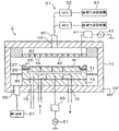
Below, with reference to accompanying drawing, preferred implementation of the present invention is described.Fig. 1 is the key diagram of brief configuration of the plasma processing apparatus 1 of expression execution mode of the present invention.Fig. 2 amplifies the longitudinal section of expression with the focusing ring 25 that this plasma processing unit 1 has.In addition, in this specification and accompanying drawing, have the structural element of identical functions structure in fact, use identical symbolic representation, omit repeat specification.
In the inside of the treatment chamber 10 of the drum that constitutes airtightly, dispose and be used for carrying the carrying of double as lower electrode of putting and put platform 11 as the semiconductor wafer W that is processed substrate.These treatment chamber 10 are put platform 11 and for example are made up of conductive materials such as aluminium with carrying.But, carry and to put the insulation board 12 of platform 11 through pottery etc., be supported on the bottom surface of treatment chamber 10, treatment chamber 10 with carry the state that platform 11 becomes electrically insulated from one another of putting.
Carry and to put platform 11 and have and be used to adsorb the not shown electrostatic chuck that keeps being placed semiconductor wafer W in the above.In addition, have carrying the set inside put platform 11: be used to make thermal medium stream 15 as the insulating properties circulation of fluid of the thermal medium of temperature control usefulness; With the gas flow path 16 that is used for the gas of helium equitemperature control usefulness is supplied to the back side of semiconductor wafer W.Like this; Through the insulating properties fluid that is controlled as set point of temperature is circulated in thermal medium stream 15; Can put platform 11 and be controlled to be set point of temperature carrying; And can the gas that temperature is controlled usefulness be supplied between the back side of putting platform 11 and semiconductor wafer W this year through gas flow path 16, promote the heat exchange between them, can be accurately, effectively semiconductor wafer W is controlled to be set point of temperature.
High frequency electric source (the RF power supply) 21 of biasing usefulness through adaptation 20 with year put platform 11 and be connected.Put the high frequency voltage that platform 11 provides assigned frequency from high frequency electric source 21 to carrying.On the other hand, treatment chamber 10 conducts with ground wire 22.
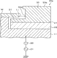
In the inside of treatment chamber 10, carry put above the platform 11 around, with surround carry put platform 11 upload the semiconductor wafer W of putting around mode, dispose focusing ring 25.This focusing ring 25 by directly carry put carry put the insulating element 26 of the ring-type on the platform 11 and be configured in this insulating element 26 above the electroconductive component 27 of ring-type constitute.Insulating element 26 for example is made up of potteries such as quartz, aluminium oxide, Vespel insulating material such as resin (dielectric) such as (registered trade marks).Electroconductive component 27 for example is made up of conductive materials such as Si (be doped with in order to produce conductivity B etc. Si), C, SiC.
As shown in Figure 2, electroconductive component 27 comprises: be configured in to carry and put the outside ring portion 30 in the outside on every side that platform 11 is uploaded the semiconductor wafer W of putting; With put platform 11 and upload below the periphery of the semiconductor wafer W of putting carrying, separate the inboard ring portion 31 of ring-type of the arranged spaced of regulation.In embodiment illustrated, outside ring portion 30 forms the electroconductive component 27 for being made up of conductive material with the inboard ring portion 31 of ring-type, therefore, and outside ring portion 30 and the state of inboard ring portion 31 for conducting each other.But as stated, at the electroconductive component 27 of ring-type and carry to put and be provided with insulating element 26 between the platform 11, therefore, outside ring portion 30 is put platform 11 electric insulations with inboard ring portion 31 with respect to carrying.In addition, outside ring portion 30 is remembered in Fig. 2 with the border of inboard ring portion 31 made dotted line 31 '.Shown in this border 31 '; In the electroconductive component that forms 27, be configured in to carry and put the part in the outside on every side that platform 11 is uploaded the semiconductor wafer W of putting, be outside ring portion 30; Below the periphery of semiconductor wafer W, the part that separates the predetermined distance configuration becomes the inboard ring portion 31 of ring-type.
In addition, with the electroconductive component 27 that carries the ring-type of putting platform 11 insulation,, except insulating element 26, do not electrically contact like this in the inside of treatment chamber 10.Therefore, outside ring portion 30 also becomes the electric state that floats with inboard ring portion 31 with respect to ground wire 22.
In addition, in the inside of treatment chamber 10,, be provided with the air exhaust loop 35 of the ring-type that is formed with a plurality of steam vents in the outside of focusing ring 25.Utilize the vacuum pump of the gas extraction system 37 that is connected with exhaust outlet 36 etc.,, carry out the vacuum exhaust in the processing space in the treatment chamber 10 through this air exhaust loop 35.
On the other hand, carrying the top put the treatment chamber 10 above the platform 11, putting platform 11 and work as pair of electrodes (upper electrode and lower electrode) with shower nozzle 40 to put platform 11 parallel relative modes and be provided with shower nozzle 40 with carrying, to carry.In addition, the high frequency electric source 42 of plasma generation usefulness is connected with this shower nozzle 40 through adaptation 41.
Then, the step to the Cement Composite Treated by Plasma of above-mentioned such plasma processing apparatus 1 that constitutes describes.
At first, open on the treatment chamber 10 the not shown gate valve that is provided with, through with the load locking room (not shown) of this gate valve disposed adjacent, utilize transport mechanism (not shown) that semiconductor wafer W is moved in the treatment chamber 10, carry to put carrying and put on the platform 11.Then, transport mechanism is kept out of the way handle chamber 10 outer after, closing gate valve, making in the treatment chamber 10 becomes air-tight state.
After this, utilize the vacuum pump of gas extraction system 37, through exhaust outlet 36, with being vented to the specified vacuum degree in the treatment chamber 10, and from handling gas supply source 53, through shower nozzle 40, supply predetermined process gas to treatment chamber 10 in.
Then; Under this state; Supply with the RF power of the lower biasing usefulness of frequency ratio and supply with the RF power that the higher plasma of frequency ratio generates usefulness from high frequency electric source 21 from high frequency electric source 42, thus, as shown in Figure 2; Above semiconductor wafer W, in treatment chamber 10, generate plasma P.Like this, free radical molecule, ion in the plasma P that will above semiconductor wafer W, generate are guided into above the semiconductor wafer W, through their effect, carry out the Cement Composite Treated by Plasma above the semiconductor wafer W.
Then, when the Cement Composite Treated by Plasma of regulation finishes, stop to stop Cement Composite Treated by Plasma thus,, semiconductor wafer W is taken out of outside the processing chamber 10 by the step opposite with above-mentioned step from high frequency electric source 21,42 supply high frequency electric power.
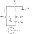
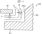
When carrying out such Cement Composite Treated by Plasma; In the plasma processing apparatus 1 of this execution mode; As previously mentioned, adopted electroconductive component 27 is configured in to carry through insulating element 26 and put the focusing ring 25 on the platform 11, therefore; As shown in Figure 3, become the state that between semiconductor wafer W (carry and put platform 11) and electroconductive component 27, produces potential difference Ve.In this case, if the static capacity of establishing between semiconductor wafer W and the electroconductive component 27 is Ce, then potential difference Ve and static capacity Ce are inversely proportional to.
In addition, in Cement Composite Treated by Plasma,, between semiconductor wafer W and electroconductive component 27, form electric field E shown in Figure 4 through between semiconductor wafer W and electroconductive component 27, producing potential difference Ve like this.The equipotential plane e of this electric field E; As shown in Figure 4, between the inner peripheral surface 30c of the outer peripheral face of semiconductor wafer W and outside ring portion 30, roughly become vertical direction; Below the periphery of semiconductor wafer W and between above the inboard ring portion 31, roughly become horizontal direction.The effect of electric field E through having such equipotential plane e; Between the inner peripheral surface 30c of the outer peripheral face of semiconductor wafer W and outside ring portion 30; Can make the ion I in the plasma P that attracts downwards towards the surface of semiconductor wafer W, on the direction of the outer peripheral face of semiconductor wafer W, quicken, in addition; Below the periphery of semiconductor wafer W and between above the inboard ring portion 31, the ion I in the plasma is quickened on the direction below the periphery of semiconductor wafer W.
Like this; In Cement Composite Treated by Plasma; Effect through the electric field E that forms by the potential difference Ve between semiconductor wafer W and the electroconductive component 27; Make and collide below outer peripheral face and the periphery of ion I and semiconductor wafer W in the plasma, thus, can reduce the outer peripheral face of semiconductor wafer W and the sedimental generation below the periphery.
In addition; For the sedimental generation below the periphery that reduces semiconductor wafer W; Between the inner peripheral surface 30c of the outer peripheral face of semiconductor wafer W and outside ring portion 30, not whole ion I and the outer peripheral face collision of semiconductor wafer W that makes in the plasma, at least a portion that makes the ion I in the plasma is directly downwards between the inner peripheral surface 30c of outer peripheral face through semiconductor wafer W and outside ring portion 30; Ion I is passed through, up to the periphery below of semiconductor wafer W.Therefore, as shown in Figure 2, with carry put platform 11 upload the semiconductor wafer W of putting outer peripheral face and with the interval L of the inner peripheral surface 30c of its opposite external side ring portion 30
1, form than the following interval L of the periphery of the top and semiconductor wafer W of inboard ring portion 31
2Wide.
Through forming such structure; Can make the interval between the equipotential plane e shown in Figure 4; Thinner between the inner peripheral surface 30c of the outer peripheral face of semiconductor wafer W and outside ring portion 30, below the periphery of semiconductor wafer W and closeer between above the inboard ring portion 31.Thus, between the inner peripheral surface 30c of the outer peripheral face of semiconductor wafer W and outside ring portion 30, can make towards less, thereby ion I is passed through, up to the periphery below of semiconductor wafer W towards the speed-up ratio of the direction of the outer peripheral face of semiconductor wafer W.In addition; On the other hand; Below the periphery of semiconductor wafer W and between above the inboard ring portion 31; Can make towards the speed-up ratio of the direction below the periphery of semiconductor wafer W greatlyyer, make and collide below the periphery of ion I and semiconductor wafer W, thereby can reduce the sedimental generation below the periphery of semiconductor wafer W reliably.
In addition, the interval L of the inner peripheral surface 30c of the outer peripheral face of semiconductor wafer W and outside ring portion 30
1And the following interval L of the periphery of the top and semiconductor wafer W of inboard ring portion 31
2Preferred range; Because of the height of the diameter of the size of the potential difference Ve that forms between semiconductor wafer W and the electroconductive component 27, semiconductor wafer W and thickness, inner peripheral surface 30c etc. changes; Therefore can not confirm entirely; But, for example, the interval L of the inner peripheral surface 30c of the outer peripheral face of semiconductor wafer W and outside ring portion 30
1Be 1~5mm, be preferably 2~2.5mm.If should interval L
1Too small, then between the outer peripheral face of semiconductor wafer W and outside ring portion 30, can produce paradoxical discharge sometimes, on the contrary, if excessive, plasma sheath and the plasma sheath on the outside ring portion 30 on the semiconductor wafer W of stating after then possibly become discontinuous.
In addition, for example, the following interval L of the periphery of the top and semiconductor wafer W of inboard ring portion 31
2Be 0.2~1mm, be preferably 0.2~0.5mm.If should interval L
2Too small; Then can produce paradoxical discharge on inboard ring portion 31 and between the periphery of semiconductor wafer W sometimes; On the contrary, if excessive, then can not make interval between the equipotential plane e below the periphery of semiconductor wafer W and closeer between above the inboard ring portion 31; Thereby ion I is fully quickened towards the direction below the periphery of semiconductor wafer W, can not fully reduce the sedimental generation below the periphery of semiconductor wafer W.In addition, devices spaced apart L like this
2The distance L of the part that the periphery of opposed inside ring portion 31 and semiconductor wafer W is overlapping
4Be preferably 0.05~0.5mm.
In addition; In the illustrated embodiment, in Cement Composite Treated by Plasma, between semiconductor wafer W and electroconductive component 27, produce potential difference Ve; Therefore, different at the plasma sheath that produces on the semiconductor wafer W with the thickness of the plasma sheath that on the outside of electroconductive component 27 ring portion 30, forms.But; In the focusing ring 25 of this execution mode; As above-mentioned; With the high facial 30b of level above the ratio semiconductor wafer W that forms laterally the facial 30a of the inclination that raises gradually above the outside ring portion 30 and form continuously with the outside of this facial 30a that tilts, therefore, can make on the semiconductor wafer W with outside ring portion 30 on the variation of thickness of plasma sheath on border relax.Thus; Can suppress the rapid variation of the electric field of semiconductor wafer W periphery; Even at the periphery of semiconductor wafer W, also can the ion I in the plasma generally perpendicularly be attracted to semiconductor wafer W above, thereby can improve plasma processing uniformity.In addition, above ring portion 30 outside forming with the facial 30b of level by the facial 30a that tilts, also can prolong the life-span of focusing ring 25 own.
In addition, the scope h of the short transverse of the facial 30a of the inclination of formation on outer ring portion 30, preferably the height above semiconductor wafer W is the scope of 0~6mm, more preferably 2mm~4mm.In addition, the length h ' of the horizontal direction of the facial 30a that tilts (the diametric length of semiconductor wafer W) is preferably the scope of 0.5~9mm, and preferred scope is 1~6mm.In addition, tilt the length h ' of horizontal direction of facial 30a because of the interval L of the inner peripheral surface 30c of the outer peripheral face of semiconductor wafer W and outside ring portion 30
1And different, also can be 0.In this case, become the shape of the facial 30a that do not tilt, but through control interval L
1, the electric field that also can suppress the periphery of semiconductor wafer W sharply changes.
In addition, in Cement Composite Treated by Plasma, produce potential difference Ve between platform 11 and the electroconductive component 27 carrying to put, therefore, if the inward flange of inboard ring portion 31 is too put platform 11 near carrying, then might between generation paradoxical discharge.On the other hand; To put platform 11 far away excessively if the inward flange of inboard ring portion 31 is left carry; Then can not make inboard ring portion 31 fully enter into the periphery below of semiconductor wafer W; Can not as above-mentioned, make and collide below ion I and the semiconductor wafer W periphery in the plasma, can not fully obtain reducing sedimental action effect.Therefore, the inward flange of inboard ring portion 31 shown in Figure 2 with carry the interval L put platform 11
3Be preferably the scope of 0.5~1mm.
Make the static capacity Ce between semiconductor wafer W and the electroconductive component 27 reach what degree, need confirm according to each plasma processing apparatus of reality.Usually, if static capacity Ce is reduced, it is big that the potential difference Ve that then between semiconductor wafer W and electroconductive component 27, forms becomes.Therefore; Below the periphery of semiconductor wafer W and between above the inboard ring portion 31; The power that ion I in the plasma is quickened towards the direction below the periphery of semiconductor wafer W strengthens, and the effect that the sedimental generation below the periphery of semiconductor wafer W is reduced has the trend of increase.On the contrary, if static capacity Ce is increased, the potential difference Ve that then between semiconductor wafer W and electroconductive component 27, forms diminishes.Therefore; Below the periphery of semiconductor wafer W and between above the inboard ring portion 31; The power that ion I in the plasma is quickened towards the direction below the periphery of semiconductor wafer W weakens, and the effect that the sedimental generation below the periphery of semiconductor wafer W is reduced has the trend that reduces.
In addition; As stated, in Cement Composite Treated by Plasma, different with the thickness of the plasma sheath that on the outside of electroconductive component 27 ring portion 30, forms at the plasma sheath that produces on the semiconductor wafer W; Thus, the incidence angle of the ion I of the periphery of semiconductor wafer W is affected.Usually; If static capacity Ce is reduced; It is big that the potential difference Ve that then between semiconductor wafer W and electroconductive component 27, forms becomes; The thickness attenuation of the plasma sheath that in outer ring portion 30, forms, the incidence angle of ion I have in the direction towards the center of semiconductor wafer W and tilt the trend of (incidence angle>90 °).On the contrary; If static capacity Ce is increased; The potential difference Ve that then between semiconductor wafer W and electroconductive component 27, forms diminishes; The thickness thickening of the plasma sheath that in outer ring portion 30, forms, the incidence angle of ion I have in the center direction toward the outer side from semiconductor wafer W and tilt the trend of (incidence angle<90 °).
At this; The incidence angle (the left longitudinal axis) of polymer adhesion amount (the right longitudinal axis) in Fig. 5 below the expression semiconductor wafer W periphery and the ion I above the periphery of semiconductor wafer W is with respect to the analog result of the relation of the variation of the static capacity Ce between semiconductor wafer W and the electroconductive component 27.In the inventor's analog result, confirmed above-mentioned trend respectively.
So,, and compared according to the plasma processing apparatus 1 of this execution mode in the past; Can reduce the sedimental generation of a side below the periphery of semiconductor wafer W; And even the inclination of the electric field of the periphery through suppressing semiconductor wafer W is at the periphery of semiconductor wafer W; Also the etching of approximate vertical can be carried out, thereby the inner evenness of processing can be improved.
More than, represented an example of preferred implementation of the present invention, but the invention is not restricted in this illustrative mode.For example, put the interval L of inner peripheral surface 30c that platform 11 is uploaded outer peripheral face and the outside ring portion 30 of the semiconductor wafer W of putting in order to make to carry
1Broaden, focusing ring 25a that can be as shown in Figure 6 is such, with the inner peripheral surface 30c of the outer peripheral face opposite external side ring portion 30 of semiconductor wafer W on form recess 30d.Through the interval L of such formation recess 30d with the outer peripheral face of abundant expansion and semiconductor wafer W
1, ion I is passed through more smoothly, up to the periphery below of semiconductor wafer W.In addition, under the situation of this focusing ring 25a illustrated in fig. 6, preferably on outer ring portion 30, omit facial 30a.
In addition; Focusing ring 25b that also can be as shown in Figure 7 is such; Make second electroconductive component 60 that is electrically connected with ground wire 22 near disposing with carrying the electroconductive component 27 of putting platform 11 insulation, between electroconductive component 27 and electroconductive component 60, be provided with second insulating element (dielectric) 61 through insulating element 26.In addition, in this example shown in Figure 7, the cover ring (cover ring) 62 that is made up of insulating material is arranged in the arranged outside of electroconductive component 27.
In this focusing ring 25b; As shown in Figure 8; In Cement Composite Treated by Plasma, become the state that between semiconductor wafer W (carry and put platform 11) and electroconductive component 27, produces potential difference Ve and between electroconductive component 27 and ground wire 22 (electroconductive component 60), produce potential difference Vg.In this case; If the static capacity of establishing static capacity between semiconductor wafer W and the electroconductive component 27 and be between Ce, electroconductive component 27 and the ground wire 22 is Cg; Then potential difference Ve and the static capacity Ce between semiconductor wafer W (carry and put platform 11) and the electroconductive component 27 is inversely proportional to, and potential difference Vg and static capacity Cg between electroconductive component 27 and the ground wire 22 are inversely proportional to.Between these potential differences Ve, Vg, static capacity Ce, the Cg, the relation of following formula (1)~(3) is set up.
Ve+Vg=V
total (1)
Ce×Ve=Cg×Vg (2)
Ve=Cg×V
total/(Cg+Ce) (3)
Can know from formula (3),, the potential difference Ve between semiconductor wafer W (carry and put platform 11) and the electroconductive component 27 is changed through changing the static capacity Cg between electroconductive component 27 and the ground wire 22.For example in focusing ring 25b shown in Figure 7; Be arranged on the methods such as dielectric constant of second insulating element (dielectric) 61 between electroconductive component 27 and the electroconductive component 60 through what change electroconductive component 27 and second electroconductive component 60 near distance, change; Change the static capacity Cg between electroconductive component 27 and the ground wire 22; Thus, the potential difference Ve between semiconductor wafer W (carry and put platform 11) and the electroconductive component 27 is changed.
With reference to Fig. 9 this relation is described.In Fig. 9, the variation of the current potential of the semiconductor wafer W in curve W ' the expression Cement Composite Treated by Plasma, the variation of the current potential of the electroconductive component 27 in curve 27 ' the expression Cement Composite Treated by Plasma, the current potential of straight line 22 ' expression ground wire 22.In the drawings, the width between curve W ' and the curve 27 ' is the potential difference Ve between semiconductor wafer W (carry and put platform 11) and the electroconductive component 27, and the width between curve 27 ' and the straight line 22 ' is the potential difference Vg between electroconductive component 27 and the ground wire 22.Shown in Figure 9 like this, in (under the situation of the single-point line 27 ' of Fig. 9) under the situation that the potential difference Vg that makes between electroconductive component 27 and the ground wire 22 increases, the potential difference Ve between semiconductor wafer W (carry and put platform 11) and the electroconductive component 27 diminishes.On the contrary, in (under the situation of two chain-dotted lines 27 ' of Fig. 9) under the situation that the potential difference Vg that makes between electroconductive component 27 and the ground wire 22 reduces, the potential difference Ve between semiconductor wafer W (carry and put platform 11) and the electroconductive component 27 becomes big.Like this, through changing the potential difference Vg between electroconductive component 27 and the ground wire 22, can change the potential difference Ve between semiconductor wafer W (carry and put platform 11) and the electroconductive component 27.
At this; 10 expressions in the drawings: in the plasma processing apparatus 1 that uses focusing ring 27b shown in Figure 7; The incidence angle (the left longitudinal axis) of ion I above the periphery of polymer adhesion amount below the semiconductor wafer W periphery (the right longitudinal axis) and semiconductor wafer W is with respect to the analog result of the relation of the variation of the potential difference Ve between semiconductor wafer W (carry put platform 11) and the electroconductive component 27.In addition, potential difference Ve between semiconductor wafer W (carry and put platform 11) and the electroconductive component 27 and the summation (V of the potential difference Vg between electroconductive component 27 and the ground wire 22 (electroconductive component 60)
Total) be certain, according to formula (3), the potential difference Ve between semiconductor wafer W (carry and put platform 11) and the electroconductive component 27 is more proportional than (Cg/ (Cg+Ce)) with static capacity, and therefore, the transverse axis among Figure 10 uses static capacity to replace potential difference Ve than (Cg/ (Cg+Ce)).
Analog result according to the inventor; If make the potential difference Ve that between semiconductor wafer W and electroconductive component 27, forms increase (static capacity is increased than (Cg/ (Cg+Ce))); Then the sedimental generation below the periphery of semiconductor wafer W reduces, and the incidence angle of ion I has in the direction towards the center of semiconductor wafer W and tilt the trend of (incidence angle>90 °).On the contrary; If make the potential difference Ve that between semiconductor wafer W and electroconductive component 27, forms reduce (static capacity is reduced than (Cg/ (Cg+Ce))); Then the sedimental generation below the periphery of semiconductor wafer W increases, and the incidence angle of ion I has in the center direction toward the outer side from semiconductor wafer W and tilt the trend of (incidence angle<90 °).
In addition; For the potential difference Ve that between semiconductor wafer W and electroconductive component 27, forms is changed; Focusing ring 25c that can be shown in figure 11 is such; Will through insulating element 26 with carry the electroconductive component 27 of putting platform 11 insulation, the capacitor 65 through variable capacitance is electrically connected with ground wire 22.
In this focusing ring 25c; Same with the focusing ring 25b that explain in Fig. 7,8 front; In Cement Composite Treated by Plasma, become between semiconductor wafer W (carry and put platform 11) and electroconductive component 27 state that produces potential difference Ve, between electroconductive component 27 and ground wire 22 (electroconductive component 60), produces potential difference Vg.According to this focusing ring 25c, can pass through the variable capacitor 65 of operation of capacitor, change the static capacity Cg between electroconductive component 27 and the ground wire 22, therefore, can easily change the potential difference Ve between semiconductor wafer W (carry and put platform 11) and the electroconductive component 27.Through the potential difference Ve that forms between such change semiconductor wafer W and the electroconductive component 27, can easily adjust the amount of the ion I that collides below the periphery with semiconductor wafer W.
In addition, in order to change between semiconductor wafer W and electroconductive component 27 the potential difference Ve that forms, focusing ring 25d that can be shown in figure 12 is such, with variable DC power supply 66 with through insulating element 26 with year put the electroconductive component 27 that platform 11 insulate and be electrically connected.
In this focusing ring 25d; Same with the focusing ring 25b that explain in Fig. 7,8 front; In Cement Composite Treated by Plasma, become between semiconductor wafer W (carry and put platform 11) and electroconductive component 27 state that produces potential difference Ve, between electroconductive component 27 and ground wire 22 (electroconductive component 60), produces potential difference Vg.According to this focusing ring 25d, shown in figure 13 when the variable DC power supply 66 of operation, can make potential difference Vg between electroconductive component 27 and the ground wire 22 in the drawings to moving up and down.Make potential difference Vg in figure below under the situation about moving (under the situation of the single-point line 27 ' among Figure 13), the potential difference Ve between semiconductor wafer W (carry and put platform 11) and the electroconductive component 27 diminishes.On the contrary, make potential difference Vg in figure above under the situation about moving (under the situation of two chain-dotted lines 27 ' among Figure 13), semiconductor wafer W (carry and put platform 11) becomes greatly with potential difference Ve between the electroconductive component 27.Like this, through the variable DC power supply 66 that operation is connected with electroconductive component 27, can easily change the potential difference Ve between semiconductor wafer W (carry and put platform 11) and the electroconductive component 27.
In addition; More than focusing ring 25,25a, 25b, 25c, the 25d of explanation have represented to be configured in outside ring portion 30 of carrying the outside around the semiconductor wafer W of putting on the platform 11 and the inboard ring portion 31 that is configured in the periphery below of semiconductor wafer W; The form that forms as electroconductive component 27, but outside ring portion 30 also can constitute separated parts with inboard ring portion 31.In addition, under the situation that constitutes separated like this parts, outside ring portion 30 can conduct with inboard ring portion 31 each other, also can electrically insulated from one another.
Among the focusing ring 25e shown in Figure 14; Be configured in the outside ring portion 30 of carrying the outside around the semiconductor wafer W put on the platform 11 and the inboard ring portion 31 of the periphery below that is configured in semiconductor wafer W; Constitute 31 one-tenth electrically insulated from one another states of outside ring portion 30 and inboard ring portion as separated parts.In this focusing ring 25e, outside ring portion 30 is being put state held that platform 11 conducts above that with carrying.On the other hand, in inboard ring portion 31 and outside ring portion 30 with carry and put between the platform 11, be provided with insulating element 26, therefore inboard ring portion 31 is put platform 11 electric insulations with outside ring portion 30 with carrying.
In plasma processing apparatus 1 with this focusing ring 25e shown in Figure 14; In Cement Composite Treated by Plasma, outside ring portion 30 is put platform 11 and is always identical current potential with carrying, and between semiconductor wafer W and outside ring portion 30, does not produce potential difference; But because be provided with insulating element 26 between the platform 11 with year putting in inboard ring portion 31; So carry the impedance put the RF power on the platform 11 and uprise being applied to, therefore, become the only state of generation potential difference Ve between semiconductor wafer W and inboard ring portion 31.Therefore; Below the periphery of semiconductor wafer W and between above the inboard ring portion 31; Formation is quickened the ion I in the plasma on the direction below the periphery of semiconductor wafer W electric field can reduce the sedimental generation below the periphery of semiconductor wafer W.In addition; In this focusing ring 25e shown in Figure 14; Between the inner peripheral surface of the outer peripheral face of semiconductor wafer W and outside ring portion 30, do not produce potential difference; Therefore, can make ion I in the plasma smoothly between the inner peripheral surface 30c of the outer peripheral face through semiconductor wafer W and outside ring portion 30, make like this through and arrive the ion I below the periphery of semiconductor wafer W; Below the periphery of semiconductor wafer W, collide, can further reduce the sedimental generation below the periphery of semiconductor wafer W.
In addition; In Fig. 1, represented plasma is generated the example of shower nozzle 40 (upper electrode) that the higher RF power of the frequency ratio of usefulness is supplied with the top of treatment chamber 10; But also can be shown in figure 15, constitute with the high frequency electric source 21 of supplying with high frequency electric source 42 that plasma generates the higher RF power of the frequency ratio of usefulness and adaptation 41 and supplying with the lower RF power of the frequency ratio of biasing usefulness and adaptation 20 both sides all with year put platform 11 and be connected.
In addition, the present invention also can be applicable to comprise the focusing ring 25 that makes above explanation, 25a, 25b, 25c, 25d, 25e with surround carry the semiconductor wafer W of putting on the platform 11 around mode be configured in the focusing ring parts of the appropriate support parts in the treatment chamber 10.In this case, as the support component that supports focusing ring 25,25a, 25b, 25c, 25d, 25e, for example can enumerate to carry and put platform 11, air exhaust loop 35 etc.In addition, also can be with being used for support component at second electroconductive component 60 illustrated in fig. 7, second insulating element 61.
Utilizability on the industry
The present invention can use in the manufacturing industry of semiconductor device.
Claims (2)
1. plasma processing apparatus makes to be processed substrate-placing carrying in being disposed at treatment chamber and to put on the platform, through applying high frequency voltage, makes to produce plasma in the treatment chamber, handles being processed substrate, it is characterized in that:
Comprise with surround put in said year platform upload put be processed substrate around the focusing ring that disposes of mode,
Said focusing ring has: be configured in put in said year platform upload put be processed substrate around the outside ring portion outside, that constitute by conductive material; With upload below the periphery of putting that is processed substrate putting platform in said year, separate the inboard ring portion predetermined distance configuration, that constitute by conductive material with the said periphery that is processed substrate,
Said inboard ring portion and putting in said year between the platform through the insulating element electric insulation,
Second electroconductive component that is electrically connected with ground wire is near disposing through the said insulating element and the said outside ring portion of putting platform insulation in said year,
Between said outside ring portion and said second electroconductive component, be provided with second insulating element.
2. focusing ring; Through applying high frequency voltage; Make and produce plasma in the treatment chamber, to being processed in the plasma processing apparatus that substrate handles, with encirclement be configured in carrying in the said treatment chamber put on the platform be processed substrate around mode dispose; It is characterized in that, comprising:
Be configured in put in said year platform upload put be processed substrate around the outside ring portion outside, that constitute by conductive material; With upload below the periphery of putting that is processed substrate putting platform in said year, separate the inboard ring portion predetermined distance configuration, that constitute by conductive material with the said periphery that is processed substrate,
Said inboard ring portion and putting in said year between the platform through the insulating element electric insulation,
Second electroconductive component that is electrically connected with ground wire is near disposing through the said insulating element and the said outside ring portion of putting platform insulation in said year,
Between said outside ring portion and said second electroconductive component, be provided with second insulating element.
Applications Claiming Priority (2)
| Application Number | Priority Date | Filing Date | Title |
|---|---|---|---|
| JP2006074372A JP2007250967A (en) | 2006-03-17 | 2006-03-17 | Plasma treating apparatus and method, and focus ring |
| JP2006-074372 | 2006-03-17 |
Related Parent Applications (1)
| Application Number | Title | Priority Date | Filing Date |
|---|---|---|---|
| CN2007100883758A Division CN101038849B (en) | 2006-03-17 | 2007-03-16 | Plasma processing apparatus, plasma processing method and focus ring |
Publications (2)
| Publication Number | Publication Date |
|---|---|
| CN101807509A CN101807509A (en) | 2010-08-18 |
| CN101807509B true CN101807509B (en) | 2012-07-25 |
Family
ID=38594919
Family Applications (2)
| Application Number | Title | Priority Date | Filing Date |
|---|---|---|---|
| CN2007100883758A Active CN101038849B (en) | 2006-03-17 | 2007-03-16 | Plasma processing apparatus, plasma processing method and focus ring |
| CN2010101475014A Active CN101807509B (en) | 2006-03-17 | 2007-03-16 | Plasma treating apparatus and focus ring |
Family Applications Before (1)
| Application Number | Title | Priority Date | Filing Date |
|---|---|---|---|
| CN2007100883758A Active CN101038849B (en) | 2006-03-17 | 2007-03-16 | Plasma processing apparatus, plasma processing method and focus ring |
Country Status (4)
| Country | Link |
|---|---|
| JP (1) | JP2007250967A (en) |
| KR (2) | KR20070094522A (en) |
| CN (2) | CN101038849B (en) |
| TW (1) | TWI411034B (en) |
Families Citing this family (33)
| Publication number | Priority date | Publication date | Assignee | Title |
|---|---|---|---|---|
| CN101447394B (en) * | 2007-11-28 | 2012-01-11 | 北京北方微电子基地设备工艺研究中心有限责任公司 | Method for improving back pollution of work piece during manufacturing process of semiconductor |
| JP2009187673A (en) * | 2008-02-01 | 2009-08-20 | Nec Electronics Corp | Plasma treatment device and method |
| EP2283510B1 (en) * | 2008-05-02 | 2013-01-23 | Oerlikon Solar AG, Trübbach | Plasma treatment apparatus and method for plasma-assisted treatment of substrates |
| JP2010045200A (en) * | 2008-08-13 | 2010-02-25 | Tokyo Electron Ltd | Focus ring, and plasma processing apparatus and method |
| KR101592061B1 (en) * | 2008-10-31 | 2016-02-04 | 램 리써치 코포레이션 | Lower electrode assembly of plasma processing chamber |
| JP2010278166A (en) * | 2009-05-27 | 2010-12-09 | Tokyo Electron Ltd | Annular component for plasma treatment, and plasma treatment device |
| JP5227264B2 (en) | 2009-06-02 | 2013-07-03 | 東京エレクトロン株式会社 | Plasma processing apparatus, plasma processing method, program |
| JP5496568B2 (en) * | 2009-08-04 | 2014-05-21 | 東京エレクトロン株式会社 | Plasma processing apparatus and plasma processing method |
| JP2013149635A (en) * | 2010-05-11 | 2013-08-01 | Sharp Corp | Dry etching device |
| JP2013149634A (en) * | 2010-05-11 | 2013-08-01 | Sharp Corp | Dry etching device |
| JP5690596B2 (en) * | 2011-01-07 | 2015-03-25 | 東京エレクトロン株式会社 | Focus ring and substrate processing apparatus having the focus ring |
| JP2012169552A (en) * | 2011-02-16 | 2012-09-06 | Tokyo Electron Ltd | Cooling mechanism, processing chamber, component in processing chamber, and cooling method |
| JP5741124B2 (en) * | 2011-03-29 | 2015-07-01 | 東京エレクトロン株式会社 | Plasma processing equipment |
| US9412579B2 (en) * | 2012-04-26 | 2016-08-09 | Applied Materials, Inc. | Methods and apparatus for controlling substrate uniformity |
| JP6853038B2 (en) * | 2013-06-26 | 2021-03-31 | アプライド マテリアルズ インコーポレイテッドApplied Materials,Incorporated | Single ring design for high yield and reduction of substrate edge defects in ICP plasma processing chamber |
| US10047457B2 (en) * | 2013-09-16 | 2018-08-14 | Applied Materials, Inc. | EPI pre-heat ring |
| JP5767373B2 (en) * | 2014-07-29 | 2015-08-19 | 東京エレクトロン株式会社 | Plasma processing apparatus, plasma processing method, and storage medium for storing program for implementing the same |
| CN104715997A (en) * | 2015-03-30 | 2015-06-17 | 上海华力微电子有限公司 | Focusing ring and plasma processing device provided with same |
| JP6570971B2 (en) * | 2015-05-27 | 2019-09-04 | 東京エレクトロン株式会社 | Plasma processing apparatus and focus ring |
| KR102382823B1 (en) * | 2015-09-04 | 2022-04-06 | 삼성전자주식회사 | ring unit having air holes and substrate processing apparatus including the same |
| JP6607795B2 (en) * | 2016-01-25 | 2019-11-20 | 東京エレクトロン株式会社 | Substrate processing equipment |
| JP6698502B2 (en) * | 2016-11-21 | 2020-05-27 | 東京エレクトロン株式会社 | Mounting table and plasma processing device |
| KR102581226B1 (en) * | 2016-12-23 | 2023-09-20 | 삼성전자주식회사 | Plasma processing device |
| KR102205922B1 (en) * | 2017-03-31 | 2021-01-22 | 베이징 이타운 세미컨덕터 테크놀로지 컴퍼니 리미티드 | Prevents material deposition on the workpiece in the process |
| KR102063108B1 (en) * | 2017-10-30 | 2020-01-08 | 세메스 주식회사 | Apparatus and method for treating substrate |
| JP7055040B2 (en) * | 2018-03-07 | 2022-04-15 | 東京エレクトロン株式会社 | Placement device and processing device for the object to be processed |
| CN112166650B (en) * | 2018-05-30 | 2023-06-20 | 东芝三菱电机产业系统株式会社 | Active gas generating device |
| JP2019220497A (en) * | 2018-06-15 | 2019-12-26 | 東京エレクトロン株式会社 | Mounting table and plasma processing device |
| US11094511B2 (en) * | 2018-11-13 | 2021-08-17 | Applied Materials, Inc. | Processing chamber with substrate edge enhancement processing |
| JP7258562B2 (en) * | 2019-01-11 | 2023-04-17 | 東京エレクトロン株式会社 | Processing method and plasma processing apparatus |
| JP7278160B2 (en) * | 2019-07-01 | 2023-05-19 | 東京エレクトロン株式会社 | Etching method and plasma processing apparatus |
| JP7278896B2 (en) * | 2019-07-16 | 2023-05-22 | 東京エレクトロン株式会社 | Plasma processing method and plasma processing apparatus |
| KR102175990B1 (en) * | 2020-01-09 | 2020-11-09 | 하나머티리얼즈(주) | Focus Ring and plasma device including the same |
Citations (3)
| Publication number | Priority date | Publication date | Assignee | Title |
|---|---|---|---|---|
| WO2001050497A1 (en) * | 1999-12-30 | 2001-07-12 | Lam Research Corporation | Electrode assembly |
| US6344105B1 (en) * | 1999-06-30 | 2002-02-05 | Lam Research Corporation | Techniques for improving etch rate uniformity |
| CN1682344A (en) * | 2002-09-18 | 2005-10-12 | 朗姆研究公司 | Method and apparatus for the compensation of edge ring wear in a plasma processing chamber |
Family Cites Families (16)
| Publication number | Priority date | Publication date | Assignee | Title |
|---|---|---|---|---|
| JP3205878B2 (en) * | 1991-10-22 | 2001-09-04 | アネルバ株式会社 | Dry etching equipment |
| JP3531511B2 (en) * | 1998-12-22 | 2004-05-31 | 株式会社日立製作所 | Plasma processing equipment |
| JP2001185542A (en) * | 1999-12-27 | 2001-07-06 | Hitachi Ltd | Plasma processor and plasma processing method using the same |
| JP2001196357A (en) * | 2000-01-11 | 2001-07-19 | Matsushita Electric Ind Co Ltd | Plasma treatment device |
| JP2002110652A (en) * | 2000-10-03 | 2002-04-12 | Rohm Co Ltd | Plasma treatment method and its device |
| JP4676074B2 (en) * | 2001-02-15 | 2011-04-27 | 東京エレクトロン株式会社 | Focus ring and plasma processing apparatus |
| US6554954B2 (en) * | 2001-04-03 | 2003-04-29 | Applied Materials Inc. | Conductive collar surrounding semiconductor workpiece in plasma chamber |
| TWI234417B (en) * | 2001-07-10 | 2005-06-11 | Tokyo Electron Ltd | Plasma procesor and plasma processing method |
| US6887340B2 (en) * | 2001-11-13 | 2005-05-03 | Lam Research Corporation | Etch rate uniformity |
| JP4370789B2 (en) * | 2002-07-12 | 2009-11-25 | 東京エレクトロン株式会社 | Plasma processing apparatus and variable impedance means calibration method |
| JP2004200219A (en) * | 2002-12-16 | 2004-07-15 | Tokyo Electron Ltd | Treatment equipment and treatment method |
| TW200520632A (en) * | 2003-09-05 | 2005-06-16 | Tokyo Electron Ltd | Focus ring and plasma processing apparatus |
| JP4640922B2 (en) * | 2003-09-05 | 2011-03-02 | 東京エレクトロン株式会社 | Plasma processing equipment |
| KR100578129B1 (en) * | 2003-09-19 | 2006-05-10 | 삼성전자주식회사 | Plasma Etching Machine |
| JP2005303099A (en) | 2004-04-14 | 2005-10-27 | Hitachi High-Technologies Corp | Apparatus and method for plasma processing |
| EP2479783B1 (en) * | 2004-06-21 | 2018-12-12 | Tokyo Electron Limited | Plasma processing apparatus and method |
-
2006
- 2006-03-17 JP JP2006074372A patent/JP2007250967A/en active Pending
-
2007
- 2007-03-15 KR KR1020070025713A patent/KR20070094522A/en not_active Application Discontinuation
- 2007-03-16 CN CN2007100883758A patent/CN101038849B/en active Active
- 2007-03-16 TW TW096109199A patent/TWI411034B/en active
- 2007-03-16 CN CN2010101475014A patent/CN101807509B/en active Active
-
2009
- 2009-02-04 KR KR1020090008912A patent/KR100959706B1/en active IP Right Grant
Patent Citations (3)
| Publication number | Priority date | Publication date | Assignee | Title |
|---|---|---|---|---|
| US6344105B1 (en) * | 1999-06-30 | 2002-02-05 | Lam Research Corporation | Techniques for improving etch rate uniformity |
| WO2001050497A1 (en) * | 1999-12-30 | 2001-07-12 | Lam Research Corporation | Electrode assembly |
| CN1682344A (en) * | 2002-09-18 | 2005-10-12 | 朗姆研究公司 | Method and apparatus for the compensation of edge ring wear in a plasma processing chamber |
Also Published As
| Publication number | Publication date |
|---|---|
| KR20070094522A (en) | 2007-09-20 |
| CN101038849B (en) | 2010-05-26 |
| TWI411034B (en) | 2013-10-01 |
| KR20090026321A (en) | 2009-03-12 |
| CN101807509A (en) | 2010-08-18 |
| KR100959706B1 (en) | 2010-05-25 |
| CN101038849A (en) | 2007-09-19 |
| TW200741860A (en) | 2007-11-01 |
| JP2007250967A (en) | 2007-09-27 |
Similar Documents
| Publication | Publication Date | Title |
|---|---|---|
| CN101807509B (en) | Plasma treating apparatus and focus ring | |
| US7988814B2 (en) | Plasma processing apparatus, plasma processing method, focus ring, and focus ring component | |
| KR102098698B1 (en) | Plasma processing apparatus | |
| KR101486433B1 (en) | Plasma processing apparatus and sample stage | |
| US10544508B2 (en) | Controlling temperature in substrate processing systems | |
| KR101283830B1 (en) | Improvement of etch rate uniformity using the independent movement of electrode pieces | |
| TW202211733A (en) | Process chamber for cyclic and selective material removal and etching | |
| JPWO2015141521A1 (en) | Substrate processing apparatus, semiconductor device manufacturing method, and program | |
| TW201907760A (en) | RF plasma reactor having a function of tuning low frequency RF power distribution and a method applied to the plasma reactor | |
| TWI448215B (en) | Apparatus for plasma processing | |
| KR102116474B1 (en) | Substrate processing apparatus and substrate processing method | |
| KR20090026314A (en) | Apparatus for substrate processing and methods therefor | |
| JP4935149B2 (en) | Electrode plate for plasma processing and plasma processing apparatus | |
| US20150053645A1 (en) | Plasma processing apparatus and plasma processing method | |
| EP2538432A2 (en) | Plasma processing apparatus | |
| KR101898079B1 (en) | Plasma processing apparatus | |
| JP5602282B2 (en) | Plasma processing apparatus and focus ring and focus ring component | |
| CN111354672A (en) | Electrostatic chuck and plasma processing apparatus | |
| TWI679675B (en) | Capacitive coupling plasma processing device and plasma processing method | |
| KR102256216B1 (en) | Plasma processing apparatus and method | |
| JPH11283940A (en) | Plasma treatment method | |
| JPH06302678A (en) | Electrostatic chuck | |
| JP5313375B2 (en) | Plasma processing apparatus and focus ring and focus ring component | |
| US6917508B2 (en) | Apparatus for manufacturing semiconductor device | |
| JP2019110312A (en) | Plasma processing method |
Legal Events
| Date | Code | Title | Description |
|---|---|---|---|
| C06 | Publication | ||
| PB01 | Publication | ||
| C10 | Entry into substantive examination | ||
| SE01 | Entry into force of request for substantive examination | ||
| C14 | Grant of patent or utility model | ||
| GR01 | Patent grant |