CN102067310B - 带有边缘触头的晶片级芯片规模封装的堆叠及其制造方法 - Google Patents
带有边缘触头的晶片级芯片规模封装的堆叠及其制造方法 Download PDFInfo
- Publication number
- CN102067310B CN102067310B CN2009801225230A CN200980122523A CN102067310B CN 102067310 B CN102067310 B CN 102067310B CN 2009801225230 A CN2009801225230 A CN 2009801225230A CN 200980122523 A CN200980122523 A CN 200980122523A CN 102067310 B CN102067310 B CN 102067310B
- Authority
- CN
- China
- Prior art keywords
- microelectronic device
- conducting element
- micromodule
- microelectronic
- edge surface
- Prior art date
- Legal status (The legal status is an assumption and is not a legal conclusion. Google has not performed a legal analysis and makes no representation as to the accuracy of the status listed.)
- Active
Links
Images


Classifications
-
- H—ELECTRICITY
- H01—ELECTRIC ELEMENTS
- H01L—SEMICONDUCTOR DEVICES NOT COVERED BY CLASS H10
- H01L25/00—Assemblies consisting of a plurality of individual semiconductor or other solid state devices ; Multistep manufacturing processes thereof
- H01L25/03—Assemblies consisting of a plurality of individual semiconductor or other solid state devices ; Multistep manufacturing processes thereof all the devices being of a type provided for in the same subgroup of groups H01L27/00 - H01L33/00, or in a single subclass of H10K, H10N, e.g. assemblies of rectifier diodes
- H01L25/10—Assemblies consisting of a plurality of individual semiconductor or other solid state devices ; Multistep manufacturing processes thereof all the devices being of a type provided for in the same subgroup of groups H01L27/00 - H01L33/00, or in a single subclass of H10K, H10N, e.g. assemblies of rectifier diodes the devices having separate containers
- H01L25/105—Assemblies consisting of a plurality of individual semiconductor or other solid state devices ; Multistep manufacturing processes thereof all the devices being of a type provided for in the same subgroup of groups H01L27/00 - H01L33/00, or in a single subclass of H10K, H10N, e.g. assemblies of rectifier diodes the devices having separate containers the devices being of a type provided for in group H01L27/00
-
- H—ELECTRICITY
- H01—ELECTRIC ELEMENTS
- H01L—SEMICONDUCTOR DEVICES NOT COVERED BY CLASS H10
- H01L23/00—Details of semiconductor or other solid state devices
- H01L23/48—Arrangements for conducting electric current to or from the solid state body in operation, e.g. leads, terminal arrangements ; Selection of materials therefor
-
- H—ELECTRICITY
- H01—ELECTRIC ELEMENTS
- H01L—SEMICONDUCTOR DEVICES NOT COVERED BY CLASS H10
- H01L23/00—Details of semiconductor or other solid state devices
- H01L23/12—Mountings, e.g. non-detachable insulating substrates
-
- H—ELECTRICITY
- H01—ELECTRIC ELEMENTS
- H01L—SEMICONDUCTOR DEVICES NOT COVERED BY CLASS H10
- H01L23/00—Details of semiconductor or other solid state devices
- H01L23/28—Encapsulations, e.g. encapsulating layers, coatings, e.g. for protection
- H01L23/31—Encapsulations, e.g. encapsulating layers, coatings, e.g. for protection characterised by the arrangement or shape
- H01L23/3107—Encapsulations, e.g. encapsulating layers, coatings, e.g. for protection characterised by the arrangement or shape the device being completely enclosed
- H01L23/3114—Encapsulations, e.g. encapsulating layers, coatings, e.g. for protection characterised by the arrangement or shape the device being completely enclosed the device being a chip scale package, e.g. CSP
-
- H—ELECTRICITY
- H01—ELECTRIC ELEMENTS
- H01L—SEMICONDUCTOR DEVICES NOT COVERED BY CLASS H10
- H01L24/00—Arrangements for connecting or disconnecting semiconductor or solid-state bodies; Methods or apparatus related thereto
- H01L24/01—Means for bonding being attached to, or being formed on, the surface to be connected, e.g. chip-to-package, die-attach, "first-level" interconnects; Manufacturing methods related thereto
- H01L24/02—Bonding areas ; Manufacturing methods related thereto
- H01L24/03—Manufacturing methods
-
- H—ELECTRICITY
- H01—ELECTRIC ELEMENTS
- H01L—SEMICONDUCTOR DEVICES NOT COVERED BY CLASS H10
- H01L24/00—Arrangements for connecting or disconnecting semiconductor or solid-state bodies; Methods or apparatus related thereto
- H01L24/01—Means for bonding being attached to, or being formed on, the surface to be connected, e.g. chip-to-package, die-attach, "first-level" interconnects; Manufacturing methods related thereto
- H01L24/02—Bonding areas ; Manufacturing methods related thereto
- H01L24/04—Structure, shape, material or disposition of the bonding areas prior to the connecting process
- H01L24/05—Structure, shape, material or disposition of the bonding areas prior to the connecting process of an individual bonding area
-
- H—ELECTRICITY
- H01—ELECTRIC ELEMENTS
- H01L—SEMICONDUCTOR DEVICES NOT COVERED BY CLASS H10
- H01L24/00—Arrangements for connecting or disconnecting semiconductor or solid-state bodies; Methods or apparatus related thereto
- H01L24/01—Means for bonding being attached to, or being formed on, the surface to be connected, e.g. chip-to-package, die-attach, "first-level" interconnects; Manufacturing methods related thereto
- H01L24/02—Bonding areas ; Manufacturing methods related thereto
- H01L24/07—Structure, shape, material or disposition of the bonding areas after the connecting process
- H01L24/08—Structure, shape, material or disposition of the bonding areas after the connecting process of an individual bonding area
-
- H—ELECTRICITY
- H01—ELECTRIC ELEMENTS
- H01L—SEMICONDUCTOR DEVICES NOT COVERED BY CLASS H10
- H01L24/00—Arrangements for connecting or disconnecting semiconductor or solid-state bodies; Methods or apparatus related thereto
- H01L24/01—Means for bonding being attached to, or being formed on, the surface to be connected, e.g. chip-to-package, die-attach, "first-level" interconnects; Manufacturing methods related thereto
- H01L24/18—High density interconnect [HDI] connectors; Manufacturing methods related thereto
- H01L24/23—Structure, shape, material or disposition of the high density interconnect connectors after the connecting process
- H01L24/24—Structure, shape, material or disposition of the high density interconnect connectors after the connecting process of an individual high density interconnect connector
-
- H—ELECTRICITY
- H01—ELECTRIC ELEMENTS
- H01L—SEMICONDUCTOR DEVICES NOT COVERED BY CLASS H10
- H01L24/00—Arrangements for connecting or disconnecting semiconductor or solid-state bodies; Methods or apparatus related thereto
- H01L24/73—Means for bonding being of different types provided for in two or more of groups H01L24/10, H01L24/18, H01L24/26, H01L24/34, H01L24/42, H01L24/50, H01L24/63, H01L24/71
-
- H—ELECTRICITY
- H01—ELECTRIC ELEMENTS
- H01L—SEMICONDUCTOR DEVICES NOT COVERED BY CLASS H10
- H01L24/00—Arrangements for connecting or disconnecting semiconductor or solid-state bodies; Methods or apparatus related thereto
- H01L24/80—Methods for connecting semiconductor or other solid state bodies using means for bonding being attached to, or being formed on, the surface to be connected
- H01L24/82—Methods for connecting semiconductor or other solid state bodies using means for bonding being attached to, or being formed on, the surface to be connected by forming build-up interconnects at chip-level, e.g. for high density interconnects [HDI]
-
- H—ELECTRICITY
- H01—ELECTRIC ELEMENTS
- H01L—SEMICONDUCTOR DEVICES NOT COVERED BY CLASS H10
- H01L24/00—Arrangements for connecting or disconnecting semiconductor or solid-state bodies; Methods or apparatus related thereto
- H01L24/91—Methods for connecting semiconductor or solid state bodies including different methods provided for in two or more of groups H01L24/80 - H01L24/90
- H01L24/92—Specific sequence of method steps
-
- H—ELECTRICITY
- H01—ELECTRIC ELEMENTS
- H01L—SEMICONDUCTOR DEVICES NOT COVERED BY CLASS H10
- H01L25/00—Assemblies consisting of a plurality of individual semiconductor or other solid state devices ; Multistep manufacturing processes thereof
- H01L25/03—Assemblies consisting of a plurality of individual semiconductor or other solid state devices ; Multistep manufacturing processes thereof all the devices being of a type provided for in the same subgroup of groups H01L27/00 - H01L33/00, or in a single subclass of H10K, H10N, e.g. assemblies of rectifier diodes
- H01L25/04—Assemblies consisting of a plurality of individual semiconductor or other solid state devices ; Multistep manufacturing processes thereof all the devices being of a type provided for in the same subgroup of groups H01L27/00 - H01L33/00, or in a single subclass of H10K, H10N, e.g. assemblies of rectifier diodes the devices not having separate containers
- H01L25/065—Assemblies consisting of a plurality of individual semiconductor or other solid state devices ; Multistep manufacturing processes thereof all the devices being of a type provided for in the same subgroup of groups H01L27/00 - H01L33/00, or in a single subclass of H10K, H10N, e.g. assemblies of rectifier diodes the devices not having separate containers the devices being of a type provided for in group H01L27/00
- H01L25/0657—Stacked arrangements of devices
-
- H—ELECTRICITY
- H01—ELECTRIC ELEMENTS
- H01L—SEMICONDUCTOR DEVICES NOT COVERED BY CLASS H10
- H01L25/00—Assemblies consisting of a plurality of individual semiconductor or other solid state devices ; Multistep manufacturing processes thereof
- H01L25/50—Multistep manufacturing processes of assemblies consisting of devices, each device being of a type provided for in group H01L27/00 or H01L29/00
-
- H—ELECTRICITY
- H01—ELECTRIC ELEMENTS
- H01L—SEMICONDUCTOR DEVICES NOT COVERED BY CLASS H10
- H01L2224/00—Indexing scheme for arrangements for connecting or disconnecting semiconductor or solid-state bodies and methods related thereto as covered by H01L24/00
- H01L2224/01—Means for bonding being attached to, or being formed on, the surface to be connected, e.g. chip-to-package, die-attach, "first-level" interconnects; Manufacturing methods related thereto
- H01L2224/02—Bonding areas; Manufacturing methods related thereto
- H01L2224/023—Redistribution layers [RDL] for bonding areas
- H01L2224/0231—Manufacturing methods of the redistribution layers
-
- H—ELECTRICITY
- H01—ELECTRIC ELEMENTS
- H01L—SEMICONDUCTOR DEVICES NOT COVERED BY CLASS H10
- H01L2224/00—Indexing scheme for arrangements for connecting or disconnecting semiconductor or solid-state bodies and methods related thereto as covered by H01L24/00
- H01L2224/01—Means for bonding being attached to, or being formed on, the surface to be connected, e.g. chip-to-package, die-attach, "first-level" interconnects; Manufacturing methods related thereto
- H01L2224/02—Bonding areas; Manufacturing methods related thereto
- H01L2224/023—Redistribution layers [RDL] for bonding areas
- H01L2224/0235—Shape of the redistribution layers
- H01L2224/02351—Shape of the redistribution layers comprising interlocking features
-
- H—ELECTRICITY
- H01—ELECTRIC ELEMENTS
- H01L—SEMICONDUCTOR DEVICES NOT COVERED BY CLASS H10
- H01L2224/00—Indexing scheme for arrangements for connecting or disconnecting semiconductor or solid-state bodies and methods related thereto as covered by H01L24/00
- H01L2224/01—Means for bonding being attached to, or being formed on, the surface to be connected, e.g. chip-to-package, die-attach, "first-level" interconnects; Manufacturing methods related thereto
- H01L2224/02—Bonding areas; Manufacturing methods related thereto
- H01L2224/023—Redistribution layers [RDL] for bonding areas
- H01L2224/0237—Disposition of the redistribution layers
- H01L2224/02371—Disposition of the redistribution layers connecting the bonding area on a surface of the semiconductor or solid-state body with another surface of the semiconductor or solid-state body
-
- H—ELECTRICITY
- H01—ELECTRIC ELEMENTS
- H01L—SEMICONDUCTOR DEVICES NOT COVERED BY CLASS H10
- H01L2224/00—Indexing scheme for arrangements for connecting or disconnecting semiconductor or solid-state bodies and methods related thereto as covered by H01L24/00
- H01L2224/01—Means for bonding being attached to, or being formed on, the surface to be connected, e.g. chip-to-package, die-attach, "first-level" interconnects; Manufacturing methods related thereto
- H01L2224/02—Bonding areas; Manufacturing methods related thereto
- H01L2224/023—Redistribution layers [RDL] for bonding areas
- H01L2224/0237—Disposition of the redistribution layers
- H01L2224/02381—Side view
-
- H—ELECTRICITY
- H01—ELECTRIC ELEMENTS
- H01L—SEMICONDUCTOR DEVICES NOT COVERED BY CLASS H10
- H01L2224/00—Indexing scheme for arrangements for connecting or disconnecting semiconductor or solid-state bodies and methods related thereto as covered by H01L24/00
- H01L2224/01—Means for bonding being attached to, or being formed on, the surface to be connected, e.g. chip-to-package, die-attach, "first-level" interconnects; Manufacturing methods related thereto
- H01L2224/02—Bonding areas; Manufacturing methods related thereto
- H01L2224/03—Manufacturing methods
- H01L2224/03001—Involving a temporary auxiliary member not forming part of the manufacturing apparatus, e.g. removable or sacrificial coating, film or substrate
- H01L2224/03002—Involving a temporary auxiliary member not forming part of the manufacturing apparatus, e.g. removable or sacrificial coating, film or substrate for supporting the semiconductor or solid-state body
-
- H—ELECTRICITY
- H01—ELECTRIC ELEMENTS
- H01L—SEMICONDUCTOR DEVICES NOT COVERED BY CLASS H10
- H01L2224/00—Indexing scheme for arrangements for connecting or disconnecting semiconductor or solid-state bodies and methods related thereto as covered by H01L24/00
- H01L2224/01—Means for bonding being attached to, or being formed on, the surface to be connected, e.g. chip-to-package, die-attach, "first-level" interconnects; Manufacturing methods related thereto
- H01L2224/02—Bonding areas; Manufacturing methods related thereto
- H01L2224/04—Structure, shape, material or disposition of the bonding areas prior to the connecting process
- H01L2224/0401—Bonding areas specifically adapted for bump connectors, e.g. under bump metallisation [UBM]
-
- H—ELECTRICITY
- H01—ELECTRIC ELEMENTS
- H01L—SEMICONDUCTOR DEVICES NOT COVERED BY CLASS H10
- H01L2224/00—Indexing scheme for arrangements for connecting or disconnecting semiconductor or solid-state bodies and methods related thereto as covered by H01L24/00
- H01L2224/01—Means for bonding being attached to, or being formed on, the surface to be connected, e.g. chip-to-package, die-attach, "first-level" interconnects; Manufacturing methods related thereto
- H01L2224/02—Bonding areas; Manufacturing methods related thereto
- H01L2224/04—Structure, shape, material or disposition of the bonding areas prior to the connecting process
- H01L2224/05—Structure, shape, material or disposition of the bonding areas prior to the connecting process of an individual bonding area
- H01L2224/0554—External layer
- H01L2224/05541—Structure
- H01L2224/05548—Bonding area integrally formed with a redistribution layer on the semiconductor or solid-state body
-
- H—ELECTRICITY
- H01—ELECTRIC ELEMENTS
- H01L—SEMICONDUCTOR DEVICES NOT COVERED BY CLASS H10
- H01L2224/00—Indexing scheme for arrangements for connecting or disconnecting semiconductor or solid-state bodies and methods related thereto as covered by H01L24/00
- H01L2224/01—Means for bonding being attached to, or being formed on, the surface to be connected, e.g. chip-to-package, die-attach, "first-level" interconnects; Manufacturing methods related thereto
- H01L2224/02—Bonding areas; Manufacturing methods related thereto
- H01L2224/04—Structure, shape, material or disposition of the bonding areas prior to the connecting process
- H01L2224/05—Structure, shape, material or disposition of the bonding areas prior to the connecting process of an individual bonding area
- H01L2224/0554—External layer
- H01L2224/0555—Shape
- H01L2224/05556—Shape in side view
- H01L2224/05558—Shape in side view conformal layer on a patterned surface
-
- H—ELECTRICITY
- H01—ELECTRIC ELEMENTS
- H01L—SEMICONDUCTOR DEVICES NOT COVERED BY CLASS H10
- H01L2224/00—Indexing scheme for arrangements for connecting or disconnecting semiconductor or solid-state bodies and methods related thereto as covered by H01L24/00
- H01L2224/01—Means for bonding being attached to, or being formed on, the surface to be connected, e.g. chip-to-package, die-attach, "first-level" interconnects; Manufacturing methods related thereto
- H01L2224/02—Bonding areas; Manufacturing methods related thereto
- H01L2224/04—Structure, shape, material or disposition of the bonding areas prior to the connecting process
- H01L2224/06—Structure, shape, material or disposition of the bonding areas prior to the connecting process of a plurality of bonding areas
- H01L2224/061—Disposition
- H01L2224/0612—Layout
- H01L2224/0615—Mirror array, i.e. array having only a reflection symmetry, i.e. bilateral symmetry
- H01L2224/06154—Mirror array, i.e. array having only a reflection symmetry, i.e. bilateral symmetry covering only portions of the surface to be connected
- H01L2224/06155—Covering only the peripheral area of the surface to be connected, i.e. peripheral arrangements
-
- H—ELECTRICITY
- H01—ELECTRIC ELEMENTS
- H01L—SEMICONDUCTOR DEVICES NOT COVERED BY CLASS H10
- H01L2224/00—Indexing scheme for arrangements for connecting or disconnecting semiconductor or solid-state bodies and methods related thereto as covered by H01L24/00
- H01L2224/01—Means for bonding being attached to, or being formed on, the surface to be connected, e.g. chip-to-package, die-attach, "first-level" interconnects; Manufacturing methods related thereto
- H01L2224/02—Bonding areas; Manufacturing methods related thereto
- H01L2224/04—Structure, shape, material or disposition of the bonding areas prior to the connecting process
- H01L2224/06—Structure, shape, material or disposition of the bonding areas prior to the connecting process of a plurality of bonding areas
- H01L2224/061—Disposition
- H01L2224/0618—Disposition being disposed on at least two different sides of the body, e.g. dual array
- H01L2224/06181—On opposite sides of the body
-
- H—ELECTRICITY
- H01—ELECTRIC ELEMENTS
- H01L—SEMICONDUCTOR DEVICES NOT COVERED BY CLASS H10
- H01L2224/00—Indexing scheme for arrangements for connecting or disconnecting semiconductor or solid-state bodies and methods related thereto as covered by H01L24/00
- H01L2224/01—Means for bonding being attached to, or being formed on, the surface to be connected, e.g. chip-to-package, die-attach, "first-level" interconnects; Manufacturing methods related thereto
- H01L2224/02—Bonding areas; Manufacturing methods related thereto
- H01L2224/07—Structure, shape, material or disposition of the bonding areas after the connecting process
- H01L2224/08—Structure, shape, material or disposition of the bonding areas after the connecting process of an individual bonding area
- H01L2224/081—Disposition
- H01L2224/0812—Disposition the bonding area connecting directly to another bonding area, i.e. connectorless bonding, e.g. bumpless bonding
- H01L2224/08135—Disposition the bonding area connecting directly to another bonding area, i.e. connectorless bonding, e.g. bumpless bonding the bonding area connecting between different semiconductor or solid-state bodies, i.e. chip-to-chip
- H01L2224/08145—Disposition the bonding area connecting directly to another bonding area, i.e. connectorless bonding, e.g. bumpless bonding the bonding area connecting between different semiconductor or solid-state bodies, i.e. chip-to-chip the bodies being stacked
- H01L2224/08148—Disposition the bonding area connecting directly to another bonding area, i.e. connectorless bonding, e.g. bumpless bonding the bonding area connecting between different semiconductor or solid-state bodies, i.e. chip-to-chip the bodies being stacked the bonding area connecting to a bonding area protruding from the surface of the body
-
- H—ELECTRICITY
- H01—ELECTRIC ELEMENTS
- H01L—SEMICONDUCTOR DEVICES NOT COVERED BY CLASS H10
- H01L2224/00—Indexing scheme for arrangements for connecting or disconnecting semiconductor or solid-state bodies and methods related thereto as covered by H01L24/00
- H01L2224/01—Means for bonding being attached to, or being formed on, the surface to be connected, e.g. chip-to-package, die-attach, "first-level" interconnects; Manufacturing methods related thereto
- H01L2224/02—Bonding areas; Manufacturing methods related thereto
- H01L2224/07—Structure, shape, material or disposition of the bonding areas after the connecting process
- H01L2224/09—Structure, shape, material or disposition of the bonding areas after the connecting process of a plurality of bonding areas
- H01L2224/091—Disposition
- H01L2224/0918—Disposition being disposed on at least two different sides of the body, e.g. dual array
- H01L2224/09181—On opposite sides of the body
-
- H—ELECTRICITY
- H01—ELECTRIC ELEMENTS
- H01L—SEMICONDUCTOR DEVICES NOT COVERED BY CLASS H10
- H01L2224/00—Indexing scheme for arrangements for connecting or disconnecting semiconductor or solid-state bodies and methods related thereto as covered by H01L24/00
- H01L2224/01—Means for bonding being attached to, or being formed on, the surface to be connected, e.g. chip-to-package, die-attach, "first-level" interconnects; Manufacturing methods related thereto
- H01L2224/10—Bump connectors; Manufacturing methods related thereto
- H01L2224/15—Structure, shape, material or disposition of the bump connectors after the connecting process
- H01L2224/16—Structure, shape, material or disposition of the bump connectors after the connecting process of an individual bump connector
- H01L2224/161—Disposition
- H01L2224/16135—Disposition the bump connector connecting between different semiconductor or solid-state bodies, i.e. chip-to-chip
- H01L2224/16145—Disposition the bump connector connecting between different semiconductor or solid-state bodies, i.e. chip-to-chip the bodies being stacked
- H01L2224/16148—Disposition the bump connector connecting between different semiconductor or solid-state bodies, i.e. chip-to-chip the bodies being stacked the bump connector connecting to a bonding area protruding from the surface
-
- H—ELECTRICITY
- H01—ELECTRIC ELEMENTS
- H01L—SEMICONDUCTOR DEVICES NOT COVERED BY CLASS H10
- H01L2224/00—Indexing scheme for arrangements for connecting or disconnecting semiconductor or solid-state bodies and methods related thereto as covered by H01L24/00
- H01L2224/01—Means for bonding being attached to, or being formed on, the surface to be connected, e.g. chip-to-package, die-attach, "first-level" interconnects; Manufacturing methods related thereto
- H01L2224/18—High density interconnect [HDI] connectors; Manufacturing methods related thereto
- H01L2224/23—Structure, shape, material or disposition of the high density interconnect connectors after the connecting process
- H01L2224/24—Structure, shape, material or disposition of the high density interconnect connectors after the connecting process of an individual high density interconnect connector
- H01L2224/241—Disposition
- H01L2224/24105—Connecting bonding areas at different heights
-
- H—ELECTRICITY
- H01—ELECTRIC ELEMENTS
- H01L—SEMICONDUCTOR DEVICES NOT COVERED BY CLASS H10
- H01L2224/00—Indexing scheme for arrangements for connecting or disconnecting semiconductor or solid-state bodies and methods related thereto as covered by H01L24/00
- H01L2224/01—Means for bonding being attached to, or being formed on, the surface to be connected, e.g. chip-to-package, die-attach, "first-level" interconnects; Manufacturing methods related thereto
- H01L2224/18—High density interconnect [HDI] connectors; Manufacturing methods related thereto
- H01L2224/23—Structure, shape, material or disposition of the high density interconnect connectors after the connecting process
- H01L2224/24—Structure, shape, material or disposition of the high density interconnect connectors after the connecting process of an individual high density interconnect connector
- H01L2224/241—Disposition
- H01L2224/24135—Connecting between different semiconductor or solid-state bodies, i.e. chip-to-chip
- H01L2224/24145—Connecting between different semiconductor or solid-state bodies, i.e. chip-to-chip the bodies being stacked
- H01L2224/24146—Connecting between different semiconductor or solid-state bodies, i.e. chip-to-chip the bodies being stacked the HDI interconnect connecting to the same level of the lower semiconductor or solid-state body at which the upper semiconductor or solid-state body is mounted
-
- H—ELECTRICITY
- H01—ELECTRIC ELEMENTS
- H01L—SEMICONDUCTOR DEVICES NOT COVERED BY CLASS H10
- H01L2224/00—Indexing scheme for arrangements for connecting or disconnecting semiconductor or solid-state bodies and methods related thereto as covered by H01L24/00
- H01L2224/01—Means for bonding being attached to, or being formed on, the surface to be connected, e.g. chip-to-package, die-attach, "first-level" interconnects; Manufacturing methods related thereto
- H01L2224/18—High density interconnect [HDI] connectors; Manufacturing methods related thereto
- H01L2224/23—Structure, shape, material or disposition of the high density interconnect connectors after the connecting process
- H01L2224/24—Structure, shape, material or disposition of the high density interconnect connectors after the connecting process of an individual high density interconnect connector
- H01L2224/244—Connecting portions
-
- H—ELECTRICITY
- H01—ELECTRIC ELEMENTS
- H01L—SEMICONDUCTOR DEVICES NOT COVERED BY CLASS H10
- H01L2224/00—Indexing scheme for arrangements for connecting or disconnecting semiconductor or solid-state bodies and methods related thereto as covered by H01L24/00
- H01L2224/01—Means for bonding being attached to, or being formed on, the surface to be connected, e.g. chip-to-package, die-attach, "first-level" interconnects; Manufacturing methods related thereto
- H01L2224/18—High density interconnect [HDI] connectors; Manufacturing methods related thereto
- H01L2224/23—Structure, shape, material or disposition of the high density interconnect connectors after the connecting process
- H01L2224/24—Structure, shape, material or disposition of the high density interconnect connectors after the connecting process of an individual high density interconnect connector
- H01L2224/245—Material
-
- H—ELECTRICITY
- H01—ELECTRIC ELEMENTS
- H01L—SEMICONDUCTOR DEVICES NOT COVERED BY CLASS H10
- H01L2224/00—Indexing scheme for arrangements for connecting or disconnecting semiconductor or solid-state bodies and methods related thereto as covered by H01L24/00
- H01L2224/01—Means for bonding being attached to, or being formed on, the surface to be connected, e.g. chip-to-package, die-attach, "first-level" interconnects; Manufacturing methods related thereto
- H01L2224/18—High density interconnect [HDI] connectors; Manufacturing methods related thereto
- H01L2224/23—Structure, shape, material or disposition of the high density interconnect connectors after the connecting process
- H01L2224/25—Structure, shape, material or disposition of the high density interconnect connectors after the connecting process of a plurality of high density interconnect connectors
- H01L2224/251—Disposition
- H01L2224/25105—Connecting at different heights
-
- H—ELECTRICITY
- H01—ELECTRIC ELEMENTS
- H01L—SEMICONDUCTOR DEVICES NOT COVERED BY CLASS H10
- H01L2224/00—Indexing scheme for arrangements for connecting or disconnecting semiconductor or solid-state bodies and methods related thereto as covered by H01L24/00
- H01L2224/01—Means for bonding being attached to, or being formed on, the surface to be connected, e.g. chip-to-package, die-attach, "first-level" interconnects; Manufacturing methods related thereto
- H01L2224/18—High density interconnect [HDI] connectors; Manufacturing methods related thereto
- H01L2224/23—Structure, shape, material or disposition of the high density interconnect connectors after the connecting process
- H01L2224/25—Structure, shape, material or disposition of the high density interconnect connectors after the connecting process of a plurality of high density interconnect connectors
- H01L2224/251—Disposition
- H01L2224/2512—Layout
- H01L2224/25174—Stacked arrangements
-
- H—ELECTRICITY
- H01—ELECTRIC ELEMENTS
- H01L—SEMICONDUCTOR DEVICES NOT COVERED BY CLASS H10
- H01L2224/00—Indexing scheme for arrangements for connecting or disconnecting semiconductor or solid-state bodies and methods related thereto as covered by H01L24/00
- H01L2224/01—Means for bonding being attached to, or being formed on, the surface to be connected, e.g. chip-to-package, die-attach, "first-level" interconnects; Manufacturing methods related thereto
- H01L2224/18—High density interconnect [HDI] connectors; Manufacturing methods related thereto
- H01L2224/23—Structure, shape, material or disposition of the high density interconnect connectors after the connecting process
- H01L2224/25—Structure, shape, material or disposition of the high density interconnect connectors after the connecting process of a plurality of high density interconnect connectors
- H01L2224/251—Disposition
- H01L2224/2518—Disposition being disposed on at least two different sides of the body, e.g. dual array
-
- H—ELECTRICITY
- H01—ELECTRIC ELEMENTS
- H01L—SEMICONDUCTOR DEVICES NOT COVERED BY CLASS H10
- H01L2224/00—Indexing scheme for arrangements for connecting or disconnecting semiconductor or solid-state bodies and methods related thereto as covered by H01L24/00
- H01L2224/01—Means for bonding being attached to, or being formed on, the surface to be connected, e.g. chip-to-package, die-attach, "first-level" interconnects; Manufacturing methods related thereto
- H01L2224/26—Layer connectors, e.g. plate connectors, solder or adhesive layers; Manufacturing methods related thereto
- H01L2224/28—Structure, shape, material or disposition of the layer connectors prior to the connecting process
- H01L2224/29—Structure, shape, material or disposition of the layer connectors prior to the connecting process of an individual layer connector
- H01L2224/29001—Core members of the layer connector
- H01L2224/29099—Material
- H01L2224/2919—Material with a principal constituent of the material being a polymer, e.g. polyester, phenolic based polymer, epoxy
-
- H—ELECTRICITY
- H01—ELECTRIC ELEMENTS
- H01L—SEMICONDUCTOR DEVICES NOT COVERED BY CLASS H10
- H01L2224/00—Indexing scheme for arrangements for connecting or disconnecting semiconductor or solid-state bodies and methods related thereto as covered by H01L24/00
- H01L2224/01—Means for bonding being attached to, or being formed on, the surface to be connected, e.g. chip-to-package, die-attach, "first-level" interconnects; Manufacturing methods related thereto
- H01L2224/26—Layer connectors, e.g. plate connectors, solder or adhesive layers; Manufacturing methods related thereto
- H01L2224/31—Structure, shape, material or disposition of the layer connectors after the connecting process
- H01L2224/32—Structure, shape, material or disposition of the layer connectors after the connecting process of an individual layer connector
- H01L2224/321—Disposition
- H01L2224/32135—Disposition the layer connector connecting between different semiconductor or solid-state bodies, i.e. chip-to-chip
- H01L2224/32145—Disposition the layer connector connecting between different semiconductor or solid-state bodies, i.e. chip-to-chip the bodies being stacked
-
- H—ELECTRICITY
- H01—ELECTRIC ELEMENTS
- H01L—SEMICONDUCTOR DEVICES NOT COVERED BY CLASS H10
- H01L2224/00—Indexing scheme for arrangements for connecting or disconnecting semiconductor or solid-state bodies and methods related thereto as covered by H01L24/00
- H01L2224/73—Means for bonding being of different types provided for in two or more of groups H01L2224/10, H01L2224/18, H01L2224/26, H01L2224/34, H01L2224/42, H01L2224/50, H01L2224/63, H01L2224/71
- H01L2224/732—Location after the connecting process
- H01L2224/73251—Location after the connecting process on different surfaces
- H01L2224/73267—Layer and HDI connectors
-
- H—ELECTRICITY
- H01—ELECTRIC ELEMENTS
- H01L—SEMICONDUCTOR DEVICES NOT COVERED BY CLASS H10
- H01L2224/00—Indexing scheme for arrangements for connecting or disconnecting semiconductor or solid-state bodies and methods related thereto as covered by H01L24/00
- H01L2224/80—Methods for connecting semiconductor or other solid state bodies using means for bonding being attached to, or being formed on, the surface to be connected
- H01L2224/80001—Methods for connecting semiconductor or other solid state bodies using means for bonding being attached to, or being formed on, the surface to be connected by connecting a bonding area directly to another bonding area, i.e. connectorless bonding, e.g. bumpless bonding
- H01L2224/808—Bonding techniques
-
- H—ELECTRICITY
- H01—ELECTRIC ELEMENTS
- H01L—SEMICONDUCTOR DEVICES NOT COVERED BY CLASS H10
- H01L2224/00—Indexing scheme for arrangements for connecting or disconnecting semiconductor or solid-state bodies and methods related thereto as covered by H01L24/00
- H01L2224/80—Methods for connecting semiconductor or other solid state bodies using means for bonding being attached to, or being formed on, the surface to be connected
- H01L2224/82—Methods for connecting semiconductor or other solid state bodies using means for bonding being attached to, or being formed on, the surface to be connected by forming build-up interconnects at chip-level, e.g. for high density interconnects [HDI]
- H01L2224/8236—Bonding interfaces of the semiconductor or solid state body
- H01L2224/82365—Shape, e.g. interlocking features
-
- H—ELECTRICITY
- H01—ELECTRIC ELEMENTS
- H01L—SEMICONDUCTOR DEVICES NOT COVERED BY CLASS H10
- H01L2224/00—Indexing scheme for arrangements for connecting or disconnecting semiconductor or solid-state bodies and methods related thereto as covered by H01L24/00
- H01L2224/80—Methods for connecting semiconductor or other solid state bodies using means for bonding being attached to, or being formed on, the surface to be connected
- H01L2224/82—Methods for connecting semiconductor or other solid state bodies using means for bonding being attached to, or being formed on, the surface to be connected by forming build-up interconnects at chip-level, e.g. for high density interconnects [HDI]
- H01L2224/828—Bonding techniques
- H01L2224/82801—Soldering or alloying
- H01L2224/82815—Reflow soldering
-
- H—ELECTRICITY
- H01—ELECTRIC ELEMENTS
- H01L—SEMICONDUCTOR DEVICES NOT COVERED BY CLASS H10
- H01L2224/00—Indexing scheme for arrangements for connecting or disconnecting semiconductor or solid-state bodies and methods related thereto as covered by H01L24/00
- H01L2224/91—Methods for connecting semiconductor or solid state bodies including different methods provided for in two or more of groups H01L2224/80 - H01L2224/90
- H01L2224/92—Specific sequence of method steps
- H01L2224/921—Connecting a surface with connectors of different types
- H01L2224/9212—Sequential connecting processes
- H01L2224/92142—Sequential connecting processes the first connecting process involving a layer connector
- H01L2224/92144—Sequential connecting processes the first connecting process involving a layer connector the second connecting process involving a build-up interconnect
-
- H—ELECTRICITY
- H01—ELECTRIC ELEMENTS
- H01L—SEMICONDUCTOR DEVICES NOT COVERED BY CLASS H10
- H01L2224/00—Indexing scheme for arrangements for connecting or disconnecting semiconductor or solid-state bodies and methods related thereto as covered by H01L24/00
- H01L2224/91—Methods for connecting semiconductor or solid state bodies including different methods provided for in two or more of groups H01L2224/80 - H01L2224/90
- H01L2224/92—Specific sequence of method steps
- H01L2224/922—Connecting different surfaces of the semiconductor or solid-state body with connectors of different types
- H01L2224/9222—Sequential connecting processes
- H01L2224/92242—Sequential connecting processes the first connecting process involving a layer connector
- H01L2224/92244—Sequential connecting processes the first connecting process involving a layer connector the second connecting process involving a build-up interconnect
-
- H—ELECTRICITY
- H01—ELECTRIC ELEMENTS
- H01L—SEMICONDUCTOR DEVICES NOT COVERED BY CLASS H10
- H01L2224/00—Indexing scheme for arrangements for connecting or disconnecting semiconductor or solid-state bodies and methods related thereto as covered by H01L24/00
- H01L2224/93—Batch processes
- H01L2224/94—Batch processes at wafer-level, i.e. with connecting carried out on a wafer comprising a plurality of undiced individual devices
-
- H—ELECTRICITY
- H01—ELECTRIC ELEMENTS
- H01L—SEMICONDUCTOR DEVICES NOT COVERED BY CLASS H10
- H01L2224/00—Indexing scheme for arrangements for connecting or disconnecting semiconductor or solid-state bodies and methods related thereto as covered by H01L24/00
- H01L2224/93—Batch processes
- H01L2224/95—Batch processes at chip-level, i.e. with connecting carried out on a plurality of singulated devices, i.e. on diced chips
- H01L2224/96—Batch processes at chip-level, i.e. with connecting carried out on a plurality of singulated devices, i.e. on diced chips the devices being encapsulated in a common layer, e.g. neo-wafer or pseudo-wafer, said common layer being separable into individual assemblies after connecting
-
- H—ELECTRICITY
- H01—ELECTRIC ELEMENTS
- H01L—SEMICONDUCTOR DEVICES NOT COVERED BY CLASS H10
- H01L2224/00—Indexing scheme for arrangements for connecting or disconnecting semiconductor or solid-state bodies and methods related thereto as covered by H01L24/00
- H01L2224/93—Batch processes
- H01L2224/95—Batch processes at chip-level, i.e. with connecting carried out on a plurality of singulated devices, i.e. on diced chips
- H01L2224/97—Batch processes at chip-level, i.e. with connecting carried out on a plurality of singulated devices, i.e. on diced chips the devices being connected to a common substrate, e.g. interposer, said common substrate being separable into individual assemblies after connecting
-
- H—ELECTRICITY
- H01—ELECTRIC ELEMENTS
- H01L—SEMICONDUCTOR DEVICES NOT COVERED BY CLASS H10
- H01L2225/00—Details relating to assemblies covered by the group H01L25/00 but not provided for in its subgroups
- H01L2225/03—All the devices being of a type provided for in the same subgroup of groups H01L27/00 - H01L33/648 and H10K99/00
- H01L2225/04—All the devices being of a type provided for in the same subgroup of groups H01L27/00 - H01L33/648 and H10K99/00 the devices not having separate containers
- H01L2225/065—All the devices being of a type provided for in the same subgroup of groups H01L27/00 - H01L33/648 and H10K99/00 the devices not having separate containers the devices being of a type provided for in group H01L27/00
- H01L2225/06503—Stacked arrangements of devices
- H01L2225/06551—Conductive connections on the side of the device
-
- H—ELECTRICITY
- H01—ELECTRIC ELEMENTS
- H01L—SEMICONDUCTOR DEVICES NOT COVERED BY CLASS H10
- H01L2225/00—Details relating to assemblies covered by the group H01L25/00 but not provided for in its subgroups
- H01L2225/03—All the devices being of a type provided for in the same subgroup of groups H01L27/00 - H01L33/648 and H10K99/00
- H01L2225/04—All the devices being of a type provided for in the same subgroup of groups H01L27/00 - H01L33/648 and H10K99/00 the devices not having separate containers
- H01L2225/065—All the devices being of a type provided for in the same subgroup of groups H01L27/00 - H01L33/648 and H10K99/00 the devices not having separate containers the devices being of a type provided for in group H01L27/00
- H01L2225/06503—Stacked arrangements of devices
- H01L2225/06555—Geometry of the stack, e.g. form of the devices, geometry to facilitate stacking
- H01L2225/06558—Geometry of the stack, e.g. form of the devices, geometry to facilitate stacking the devices having passive surfaces facing each other, i.e. in a back-to-back arrangement
-
- H—ELECTRICITY
- H01—ELECTRIC ELEMENTS
- H01L—SEMICONDUCTOR DEVICES NOT COVERED BY CLASS H10
- H01L2225/00—Details relating to assemblies covered by the group H01L25/00 but not provided for in its subgroups
- H01L2225/03—All the devices being of a type provided for in the same subgroup of groups H01L27/00 - H01L33/648 and H10K99/00
- H01L2225/10—All the devices being of a type provided for in the same subgroup of groups H01L27/00 - H01L33/648 and H10K99/00 the devices having separate containers
- H01L2225/1005—All the devices being of a type provided for in the same subgroup of groups H01L27/00 - H01L33/648 and H10K99/00 the devices having separate containers the devices being of a type provided for in group H01L27/00
- H01L2225/1011—All the devices being of a type provided for in the same subgroup of groups H01L27/00 - H01L33/648 and H10K99/00 the devices having separate containers the devices being of a type provided for in group H01L27/00 the containers being in a stacked arrangement
- H01L2225/1017—All the devices being of a type provided for in the same subgroup of groups H01L27/00 - H01L33/648 and H10K99/00 the devices having separate containers the devices being of a type provided for in group H01L27/00 the containers being in a stacked arrangement the lowermost container comprising a device support
- H01L2225/1035—All the devices being of a type provided for in the same subgroup of groups H01L27/00 - H01L33/648 and H10K99/00 the devices having separate containers the devices being of a type provided for in group H01L27/00 the containers being in a stacked arrangement the lowermost container comprising a device support the device being entirely enclosed by the support, e.g. high-density interconnect [HDI]
-
- H—ELECTRICITY
- H01—ELECTRIC ELEMENTS
- H01L—SEMICONDUCTOR DEVICES NOT COVERED BY CLASS H10
- H01L2225/00—Details relating to assemblies covered by the group H01L25/00 but not provided for in its subgroups
- H01L2225/03—All the devices being of a type provided for in the same subgroup of groups H01L27/00 - H01L33/648 and H10K99/00
- H01L2225/10—All the devices being of a type provided for in the same subgroup of groups H01L27/00 - H01L33/648 and H10K99/00 the devices having separate containers
- H01L2225/1005—All the devices being of a type provided for in the same subgroup of groups H01L27/00 - H01L33/648 and H10K99/00 the devices having separate containers the devices being of a type provided for in group H01L27/00
- H01L2225/1011—All the devices being of a type provided for in the same subgroup of groups H01L27/00 - H01L33/648 and H10K99/00 the devices having separate containers the devices being of a type provided for in group H01L27/00 the containers being in a stacked arrangement
- H01L2225/1047—Details of electrical connections between containers
- H01L2225/1064—Electrical connections provided on a side surface of one or more of the containers
-
- H—ELECTRICITY
- H01—ELECTRIC ELEMENTS
- H01L—SEMICONDUCTOR DEVICES NOT COVERED BY CLASS H10
- H01L24/00—Arrangements for connecting or disconnecting semiconductor or solid-state bodies; Methods or apparatus related thereto
- H01L24/01—Means for bonding being attached to, or being formed on, the surface to be connected, e.g. chip-to-package, die-attach, "first-level" interconnects; Manufacturing methods related thereto
- H01L24/10—Bump connectors ; Manufacturing methods related thereto
- H01L24/12—Structure, shape, material or disposition of the bump connectors prior to the connecting process
- H01L24/13—Structure, shape, material or disposition of the bump connectors prior to the connecting process of an individual bump connector
-
- H—ELECTRICITY
- H01—ELECTRIC ELEMENTS
- H01L—SEMICONDUCTOR DEVICES NOT COVERED BY CLASS H10
- H01L24/00—Arrangements for connecting or disconnecting semiconductor or solid-state bodies; Methods or apparatus related thereto
- H01L24/01—Means for bonding being attached to, or being formed on, the surface to be connected, e.g. chip-to-package, die-attach, "first-level" interconnects; Manufacturing methods related thereto
- H01L24/18—High density interconnect [HDI] connectors; Manufacturing methods related thereto
- H01L24/23—Structure, shape, material or disposition of the high density interconnect connectors after the connecting process
- H01L24/25—Structure, shape, material or disposition of the high density interconnect connectors after the connecting process of a plurality of high density interconnect connectors
-
- H—ELECTRICITY
- H01—ELECTRIC ELEMENTS
- H01L—SEMICONDUCTOR DEVICES NOT COVERED BY CLASS H10
- H01L24/00—Arrangements for connecting or disconnecting semiconductor or solid-state bodies; Methods or apparatus related thereto
- H01L24/01—Means for bonding being attached to, or being formed on, the surface to be connected, e.g. chip-to-package, die-attach, "first-level" interconnects; Manufacturing methods related thereto
- H01L24/26—Layer connectors, e.g. plate connectors, solder or adhesive layers; Manufacturing methods related thereto
- H01L24/31—Structure, shape, material or disposition of the layer connectors after the connecting process
- H01L24/32—Structure, shape, material or disposition of the layer connectors after the connecting process of an individual layer connector
-
- H—ELECTRICITY
- H01—ELECTRIC ELEMENTS
- H01L—SEMICONDUCTOR DEVICES NOT COVERED BY CLASS H10
- H01L24/00—Arrangements for connecting or disconnecting semiconductor or solid-state bodies; Methods or apparatus related thereto
- H01L24/93—Batch processes
- H01L24/94—Batch processes at wafer-level, i.e. with connecting carried out on a wafer comprising a plurality of undiced individual devices
-
- H—ELECTRICITY
- H01—ELECTRIC ELEMENTS
- H01L—SEMICONDUCTOR DEVICES NOT COVERED BY CLASS H10
- H01L24/00—Arrangements for connecting or disconnecting semiconductor or solid-state bodies; Methods or apparatus related thereto
- H01L24/93—Batch processes
- H01L24/95—Batch processes at chip-level, i.e. with connecting carried out on a plurality of singulated devices, i.e. on diced chips
- H01L24/96—Batch processes at chip-level, i.e. with connecting carried out on a plurality of singulated devices, i.e. on diced chips the devices being encapsulated in a common layer, e.g. neo-wafer or pseudo-wafer, said common layer being separable into individual assemblies after connecting
-
- H—ELECTRICITY
- H01—ELECTRIC ELEMENTS
- H01L—SEMICONDUCTOR DEVICES NOT COVERED BY CLASS H10
- H01L2924/00—Indexing scheme for arrangements or methods for connecting or disconnecting semiconductor or solid-state bodies as covered by H01L24/00
- H01L2924/01—Chemical elements
- H01L2924/01067—Holmium [Ho]
-
- H—ELECTRICITY
- H01—ELECTRIC ELEMENTS
- H01L—SEMICONDUCTOR DEVICES NOT COVERED BY CLASS H10
- H01L2924/00—Indexing scheme for arrangements or methods for connecting or disconnecting semiconductor or solid-state bodies as covered by H01L24/00
- H01L2924/013—Alloys
- H01L2924/0132—Binary Alloys
- H01L2924/01322—Eutectic Alloys, i.e. obtained by a liquid transforming into two solid phases
-
- Y—GENERAL TAGGING OF NEW TECHNOLOGICAL DEVELOPMENTS; GENERAL TAGGING OF CROSS-SECTIONAL TECHNOLOGIES SPANNING OVER SEVERAL SECTIONS OF THE IPC; TECHNICAL SUBJECTS COVERED BY FORMER USPC CROSS-REFERENCE ART COLLECTIONS [XRACs] AND DIGESTS
- Y10—TECHNICAL SUBJECTS COVERED BY FORMER USPC
- Y10T—TECHNICAL SUBJECTS COVERED BY FORMER US CLASSIFICATION
- Y10T29/00—Metal working
- Y10T29/49—Method of mechanical manufacture
- Y10T29/49002—Electrical device making
- Y10T29/49117—Conductor or circuit manufacturing
- Y10T29/49124—On flat or curved insulated base, e.g., printed circuit, etc.
- Y10T29/4913—Assembling to base an electrical component, e.g., capacitor, etc.
- Y10T29/49144—Assembling to base an electrical component, e.g., capacitor, etc. by metal fusion
Abstract
一种微电子组件(300)可包括第一微电子装置(200)和第二微电子装置(200)。每个微电子装置都包括带有至少一个半导体模板(104)的模板结构,并且每个微电子装置具有第一表面(201)、远离该第一表面的第二表面(203)和以除直角外的角度延伸离开第一和第二表面(201,203)的至少一个边缘表面(134)。至少一个导电元件(可包括部分110,124,122,126)沿第一表面延伸至所述边缘表面的至少之一之上和第二表面(203)之上。该第一微电子装置的至少一个导电元件导电地结合于该第二微电子装置的至少一个导电元件从而在其间提供导电路径。
Description
相关申请的交叉引用
本申请要求2008年6月16日提交的美国临时专利申请61/061953的优先权,其公开内容在此引用作为参考。
技术领域
本发明涉及封装的微电子元件及其制造方法,并且更特别地涉及可堆叠的被封装微电子模板组件。
背景技术
微电子芯片典型地为带有反向相对、基本平坦的前表面和后表面且带有在这些表面之间延伸的边缘的平板体。芯片通常在前表面上具有与芯片内的电路电连接的触头,有时也称为垫或结合垫。典型地通过用适宜材料包围芯片来封装芯片,以形成具有电接于芯片触头的端子的微电子封装。接着封装被连接于测试设备以确定已封装装置是否符合所需的性能标准。一旦被测试,通过借助适宜的连接方法如焊接将封装端子连接于印刷电路板(PCB)上的匹配焊盘(lands),封装可被连接于较大的电路如电子产品如计算机或手机的电路。
微电子封装可以晶片级被制造;也就是说,构成封装的外壳、终端和其它结构被制造的同时芯片或模板仍然为晶片形式。形成模板之后,对晶片进行多个额外加工步骤以形成晶片上的封装结构,接着晶片被切块以分离各个已封装模板。晶片级加工是优选的制造方法,因为它可提供节约成本的优点,且因为可使得每个模板封装的覆盖区(footprint)与模板自身的尺寸相同或几乎相同,这就能够非常有效地利用已封装模板要被连接到的印刷电路板上的区域。以这种方式封装的模板一般称为晶片级芯片规模封装或晶片级芯片尺寸封装(WLCSP)。
为节约封装模板安装于其的基板上的额外空间,可通过竖直堆叠多个 芯片来将多个芯片合并为单独的封装。叠层中的每个模板必须典型地为叠层中的一个或多个其它模板,或叠层安装于其上的基板,或皆为两者提供电连接机构。这就使得竖直堆叠的多个模板封装在基板上占用的表面积小于封装内所有芯片加起来的总表面积。因为当使用模板叠层时比封装单个模板时通常具有多得多的电连接,叠层中不同模板之间的电连接必须极其稳定和可靠。
发明内容
一种微电子组件可包括第一微电子装置和第二微电子装置。每个微电子装置都包括带有至少一个半导体模板的模板结构,并且每个微电子装置具有第一表面、远离该第一表面的第二表面和以除直角外的角度延伸离开第一和第二表面的至少一个边缘表面。至少一个导电元件沿第一表面延伸至所述边缘表面的至少之一之上和第二表面之上。该第一微电子装置的至少一个导电元件导电地结合于该第二微电子装置的至少一个导电元件从而在其间提供导电路径。
根据一个实施例,每个微电子装置的导电元件可包括通过镀覆到第一和第二表面之一上形成的第一元件以及通过镀覆到第一和第二表面中另一个和所述至少一个边缘表面上而形成的第二元件。在一个实施例中,第二元件被镀覆在第一元件的一些部分上。例如,第二元件沿第二元件在其上被镀覆的第一元件的这些部分延伸。
第二元件能沿第一元件的边缘延伸从而在这些边缘处与第一元件导电地接合。
例如能使用可熔性金属或使用导电膏结合第一和第二微电子装置的导电元件。在一个实施例中,第一微电子装置的第一和第二表面之一能面对第二微电子装置的第一和第二表面之一并且导电元件的暴露于相面对表面处的部分被结合在一起。例如,导电元件可包括暴露于每个微电子装置的第一或第二表面的至少之一处的导电垫并且所述各导电垫能被结合在一起。
导电元件可包括迹线和导电垫,其中至少一个导电垫与至少一个边缘面间隔开而设置。在一个特定实施例中,每个微电子装置的导电元件包括 紧挨所述至少一个边缘表面或能延伸至所述至少一个边缘表面的导电垫。
在一个特定实施例中,一个或多个微电子装置能包括多个模板。在这种情形下,包括在所述至少一个微电子装置内的至少两个半导体模板的结合垫-承载表面朝着同一方向,或它们可朝着不同方向。
所述至少一个导电元件沿其延伸的所述至少一个边缘表面可相对第一和第二表面中至少之一以50~89度角设置。
在微电子组件中,第一和第二微电子装置以竖直方向被堆叠并且第一和第二微电子装置的所述至少一个边缘表面彼此偏移。
第一和第二微电子装置的第一表面能侧向(lateral)延伸且在侧向上具有第一尺寸。在一个实施例中,第一和第二微电子装置的第一表面的侧向尺寸可为不同的。
在一个实施例中,提供了一种微电子组件,其包括第一微电子装置和第二微电子装置。每个微电子装置都能包括带有至少一个半导体模板的模板结构。每个微电子装置具有第一表面、远离该第一表面的第二表面和延伸离开第一表面的至少一个边缘表面。导电元件能沿第一表面延伸至所述边缘表面的至少之一上。该第一微电子装置的至少一个导电元件能导电地结合于该第二微电子装置的至少一个导电元件从而在其间提供导电路径。
在一个实施例中,所述至少一个边缘表面以除直角外的角度远离第一和第二表面延伸。导电元件的暴露于所述至少一个边缘表面处的边缘部分能被导电地结合以提供导电路径。能使用可熔性金属或使用导电膏结合所述边缘部分。
根据一个实施例提供了一种制造叠层微电子组件的方法。在该实施例中,第一微电子装置的主表面能被设置为与第二微电子装置的主表面相对。暴露于第一微电子装置的主表面处的导电元件能被导电地结合于暴露于第二微电子装置的主表面处的导电元件以提供其间的导电路径。每个微电子装置能包括带有至少一个半导体模板的模板结构,并且每个微电子装置能具有第一主表面、远离该第一表面的第二主表面、至少一个边缘表面、以及沿第一表面延伸至所述边缘表面的至少之一之上和第二主表面之上的至少一个导电元件。
根据一个实施例,能制造一种堆叠的微电子组件。能形成包括第一微 电子装置和第二微电子装置的叠层。每个微电子装置都能包括带有至少一个半导体模板的模板结构。每个微电子装置能具有第一表面、远离该第一表面的第二表面和延伸离开第一表面的至少一个边缘表面。至少一个导电元件能沿第一表面延伸至所述边缘表面的至少之一之上。暴露于边缘表面处的导电元件的部分能被导电地结合从而在其间提供导电路径。
在该实施例中,第一微电子装置能被置于第二微电子装置之上,并且通过加热暴露于第一微电子装置至少一个边缘表面处的导电元件附近的可熔性金属来进行结合步骤。这样可熔性金属流至暴露于第二微电子装置至少一个边缘表面处的导电元件之上。在该实施例中,可熔性金属桥接第一和第二微电子装置的导电元件之间的间隙。
在该实施例中,第一微电子装置能设在第二微电子装置之上,并且通过将可流动导电材料配送至暴露于第一微电子装置至少一个边缘表面处的导电元件上来进行结合步骤。接着导电材料可流至暴露于第二微电子装置至少一个边缘表面处的导电元件之上。
附图说明
在结合附图阅读了下面对多个实施例的描述时,能最好地理解此处描述的装置和方法,附图中相同的附图标记指的是相同或类似的部件。附图不一定是按比例绘制的;而是强调示出所示实施例的原理。
图1A示出含有多个微电子芯片的晶片的透视图。
图1B示出晶片一部分的截面图。
图1C示出根据一个实施例具有设于结合垫上的第一金属化层的晶片的单个模板(die)的透视图。
图1D-1I示出经受了额外加工步骤的类似于图1B的晶片一部分的截面图。
图2A示出根据一个实施例的分离的微电子装置的截面图。
图2B和2C示出根据一个实施例的图2A中接合结构的变型的详图。
图2D示出图2A的微电子装置的透视图。
图2E概述了用于制造根据一个实施例的最终微电子装置的工艺流程图。
图3示出根据一个实施例形成模板叠层结构的多个模板的截面图。
图4A和4B示出根据一个实施例形成图3装置的接合方法的两个变型的截面图。
图5A示出根据一个实施例包括不同元件的模板叠层结构的截面图。
图5B示出根据一个实施例包括不同元件且模板尺寸各异的模板叠层结构的截面图。
图6A示出根据一个实施例具有设在结合垫上的第一金属化层的晶片的单个模板的透视图。
图6B示出根据一个实施例带有延伸至边缘的结合垫的晶片的单个模板的透视图。
图6C-6I示出根据一个实施例经受了额外加工步骤的晶片某部分的截面图,其模板类似于图6A的模板。
图7示出根据一个实施例形成的模板叠层结构的截面图。
图8A示出根据一个实施例的模板结构的截面图。
图8B示出根据一个实施例添加有额外的可回流材料的模板叠层的截面图。
图8C示出根据一个实施例的模板叠层结构的截面图。
图9概述了根据一个实施例用于制造最终装置模板的工艺流程图。
图10A-10E示出根据一个实施例导致形成包括两个或更多个模板的模板叠层的加工步骤的截面图。
图10F示出根据一个实施例包括两个或更多个模板的模板结构的截面图。
图10G示出根据一个实施例包括图10F的多个模板结构的模板叠层结构的截面图。
图10H示出根据一个实施例在图10A中开始的那部分工艺流程的变型的截面图。
图11A-11E示出根据一个实施例导致形成模板叠层的加工步骤的截面图。
图11F示出根据一个实施例包括两个或更多个模板的模板结构的截面图。
图11G示出根据一个实施例包括图11F的多个模板结构的模板叠层结构的截面图。
具体实施方式
在本文中,导电结构“暴露在”绝缘体结构表面这样的陈述指的是导电结构可用于与以垂直于绝缘体结构表面的方向从绝缘体结构外侧朝绝缘体结构表面移动的理论点相接触。因此,暴露于绝缘体结构表面处的端子或其它导电结构可从该表面突出;可与该表面齐平;或可相对该表面凹陷且通过绝缘体内的孔或凹口被暴露。
图1A示出含有多个微电子芯片的晶片100的透视图。晶片基板102通常为半导体材料如硅,但也可由其它材料制成或为一些类型的复合材料。晶片被分割为包括微电子芯片的工作部分的部分或全部独立模板104;在额外加工后这些模板在虚线103处彼此分离。每个芯片可具有一种或更多功能且使用半导体加工的本领域技术人员公知的技术形成于基板表面的上面或下面。这些示例不作为限定——被加工的晶片100可代表各种类型的装置,包括存储器、处理器、图像传感器或其他可能性。结合垫106电接于基板之上或基板之内的电路。图1B示出晶片如图1A中示出的晶片100某部分的截面图。为清楚起见,结合垫106暴露于基板102的“前面”或接触支承面101上。结合垫106可从表面101上突起,可与该表面齐平或可相对该表面凹陷。虚线103表明每个模板之间的切割线。尽管所述的晶片可为带有形成于其内的工作部分的半导体材料,在其它情形下晶片也可为重组晶片,其中通过被设置为形成各独立模板且借助粘合剂如环氧树脂被保持在一起的多个构件来形成晶片。可选地,代替晶片100的是,该结构可以是多个模板,这些模板在如虚线103所示的其边缘处连接在一起,这种结构可为矩形如面板。这些模板的边缘可在虚线处相接并且半导体材料可为连续的未切割结构,或模板的边缘彼此隔开并且用粘合剂接合为重组结构。
图1C-1I示出根据一个实施例加工晶片的步骤。要注意,所示步骤可采用所述顺序或可选地采用不同顺序进行。在某些实施例中,两个或更多个所述步骤可合并为一个步骤。在其它实施例中,可从工艺中完全取消一 个所述步骤。在其它变型中,可能需要额外的加工步骤。
图1C为具有接触结合垫的第一金属化层110的晶片100的单个模板108的透视图。可采用某些方式如沉积或镀覆将金属膜沉积在晶片表面101上,接着膜被构图以形成金属化层。在特定实施例中,可在该表面上形成种子层(seed layer),接着该种子层被构图并随之被镀覆以形成金属化层。部分金属化层被构造为制造将用于连接被叠层的各构件的连接垫112。金属化层可被构造为再分配层。此外,金属化层的各部分作为传导迹线如金属迹线从结合垫106延伸至模板边缘。图1D为晶片如图1A中所示晶片100但添加了金属化层110的截面图。为简化起见,该附图仅示出一个连接垫区域112与每个模板上的每组结合垫106接触。要注意,根据优选设计,特定的截面可包括一个或多个单独的连接区域。
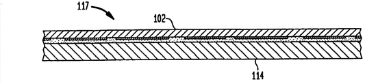
图1E示出加工晶片的下一个步骤。在图1E中,图1D中所示的组件被翻转以使金属化层110面朝下且连接于单独的临时载体基板114。使用粘合层116将临时基板114保持到第一基板102。随后,使用如研磨或抛光技术可使得第一基板102变薄为期望厚度,结果如图1F中的结构117所示。
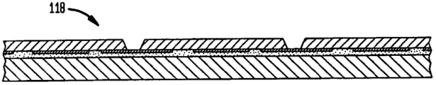
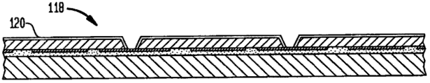
加工晶片的下一个步骤如图1G所示。在图1G中,在基板102内切割或蚀刻通道118从而打开孔以暴露第一金属化层110的一部分。在一个实施例中,这种蚀刻可通过这样的工艺进行:该工艺被控制为停止在半导体基板与金属化层之间的中间层上,接着进行部分中间层的去除以暴露金属化层110。中间层可为绝缘层。通道118可为沟槽,其作用为暴露连接于一个或多个模板的多个结合垫的各金属化层部分。图1H示出在基板102表面上形成绝缘层120的步骤。该绝缘层的目的之一是保护基板102最新暴露的表面。绝缘层将基板102与随后形成的导电结构隔绝开。通道118的底部可通过钝化层的构图沉积被保持空旷(clear),或覆盖第一金属化层的金属迹线的残留材料可在下一个步骤中被暴露。不论哪种情形,图1H的结构都在第一金属化层的一部分被暴露的情况下形成。
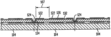
图1I示出形成沿基板102的后缘表面134和后表面132延伸的第二金属化层122的步骤。虚线还是示出了各模板104彼此分离的位置。第二金属化层122和第一金属化层一样可包括连接垫126和其它迹线。连接垫126可与模板104的边缘表面相隔一段距离107,这也在图1C中示出。也就是 说,连接垫自身不能到达边缘表面。特别要注意的是,沿模板结构边缘延伸的导电元件124将第一和第二金属化层的各部分彼此电连接。在一个实施例中,导电元件124形成为第二金属化层122的一部分并且与连接垫126和第二金属化层的相关迹线同时形成。可选地,金属化层122和导电元件124可在各单独的步骤中形成。在形成导电元件和金属化层后,基板可被切割为多个如下所述并参照图2A-D示出的独立模板结构200。概述上述步骤以制造装置200的流程图见于图2E。
第二金属化层的连接垫的尺寸、形状和位置可与第一金属化层110的连接垫相同或类似,但其它构型也是可能的。各连接垫在不同层上的排列有助于随后堆叠各个独立模板结构以形成堆叠的微电子组件如参照图3的下述组件。
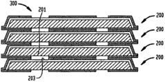
图2A示出一个实施例的微电子装置200在与相邻元件分离后的最终结构的截面图。图2D示出朝与表面201相反的装置表面203看时所见到的相应透视图,结合垫106最初暴露于该表面201之上。图2B示出导电元件124与第一金属化层110之间的示例连接的详图。图2B示出一旦如实施例之前所述完成工艺后各层之间的接头的结构。用于在其间形成类似金属化层和接头的工艺在美国专利US6972480和7192796中有描述,其公开内容在此引用作为参考。在此示例中的导电元件124沿其中第一金属化层沿表面201水平延伸的方向延伸。导电元件可被镀覆在金属化层上。导电元件的延伸超出边缘表面134的部分的长度可根据如何进行分割(singulation cut)或其它因素而改变。在一个变型中,导电元件124’与金属化层110’之间的接头如图2C所示,其中导电元件124’沿金属化层110’的边缘208延伸,边缘208在层110’的厚度方向214上远离表面201延伸。用于在导电元件之间形成带有类似接头的类似结构的工艺在美国专利US6646289和6777767中有描述,其公开内容在此引用作为参考。如果通道118被蚀刻的更深并且产生完全穿过第一金属层的在通道交叉处的部分的间隙,可得到这样的结构。在一个实施例中,微电子装置如同图2A所示的那样,可被堆叠和连接以形成叠层模板装置。这样的一个示例参见图3。在该示例中,模板叠层组件300由四个基本相同的微电子装置200组成。该叠层中的各种装置200可来自单个晶片,或来自不同晶片。为提高可靠性和产量,每个 模板装置在堆叠前可被测试以在组装前确保它是完全可使用的。通过使用已知的良好装置来形成叠层,可减轻模板叠层的复合产量问题。如上所述,这种堆叠方法可被理解为模板-级工艺,其中模板在从晶片处分离后被堆叠。
在一个实施例中,模板叠层300功能上是完整的,但也可能需要额外的步骤来将其封装为其最终的形态。任何额外的封装步骤都涉及本领域技术人员公知的技术。
在可选实施例中,可在晶片级上进行接合。在将晶片接合在一起形成叠层后,接着分离该完成的模板叠层。
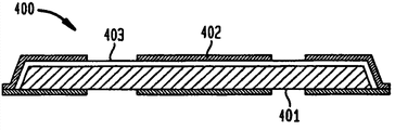
可以多种方式实现一个模板与下一层的实际接合。图4A和4B示出两个示例性方法。在图4A中,示出的微电子装置类似图2A所示的。在图4B中,例如可为可熔性冶金接合金属的导电粘合材料层412已被置于上连接垫402上。接合金属可为焊锡、锡、铟、这些金属或其它这些金属组合物的共晶体或合金,其可以不同方式被镀覆上或被沉积。如图所示,接合金属可被仅涂敷于暴露于后表面403处的连接垫402,但可以想到该工艺可将金属置于一个或更多暴露的金属表面上,这些表面包括侧面导电元件或模板表面处的其它垫。不论哪种情形下,带有接合金属的模板都接着被对齐和堆叠。接着加热该叠层以完成面对面接合。可选地,导电膏如银填充膏、金膏、焊膏等可用作导电粘合材料,从而在叠层中的微电子装置的导电元件之间形成导电路径。如图3所示,某些微电子装置的前表面201面对其它微电子装置的后表面203。某些微电子装置200的前表面201处的导电元件导电地粘合于其它微电子装置200的后表面203处的导电元件。在一个特定实施例中,两个微电子装置可被设置成使其前表面401(图4A)彼此面对。接着,暴露于微电子装置400的前表面401处的连接垫可与暴露于另一微电子装置的前表面401处的连接垫相接合。在另一实施例中,两个微电子装置的后表面能彼此面对并且这些后表面上的连接垫通过上述方法相接合。在特定实施例中,导电元件之间的结合能在彼此相面对的表面处进行,同时微电子装置200保持以晶片形式相连,例如如图1I所示。
在另一个模板叠层实施例中,模板叠层可以由具有不同功能的不同种类模板构成。图5A示出一种这样的模板叠层结构500。该模板叠层结构500 与图3中的类似,但是,叠层中的各独立装置是不同的。在此示例中,叠层中的顶部的两个模板502是相同的,但底部的两个模板(504和506)是不同的。例如,模板502可为存储元件,模板504可为存储控制器,并且模板506可为加工单元。在这样的叠层构造中,各个模板的侧向(lateral)尺寸基本相同,并且各个模板之间的连接垫也基本在相同位置处重叠。尽管模板叠层500可以模板级被组装,在可选实施例中它也能以晶片级被组装且在任何指定晶片上的晶片区域内几乎无损耗。对模板尺寸的限制是不必要的。实际上,图5B示出的实施例中,模板叠层结构510由功能和尺寸均各异的模板组成。在一个实施例中,对堆叠模板的唯一限制是相邻表面应当具有处于相同位置的连接垫。在图5B所示的实施例中,模板514在顶面和底面上都具有连接垫,它们彼此不相配但被构造为分别与模板512和516上的连接垫相配。
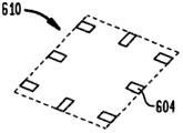
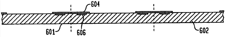
在一个实施例中,微电子装置的连接垫被置于芯片的结合垫处或其附近。对于某些构型来说,这就提供了足以形成与模板叠层内第二微电子装置的连接的金属表面可用区域。图6A示出模板600的透视图,其具有暴露于前面即接触-承载表面601处的结合垫606。该图类似于图1C。模板是带有一个或多个模板的晶片的一部分,该晶片可等同于图1A的晶片。金属化层可包括形成于芯片的结合垫之上或与其接触的连接垫604。在多种情形下,芯片的结合垫的间隔已经很小了,从而防止结合垫上的金属化层的宽度实际上比结合垫自身还宽。在本实施例的变型中,在结合垫上不提供金属层,如图6B所示。在图6B中,结合垫靠近边缘且可延伸至模板区域的边缘,从而第二金属化步骤可借助导电元件将每个结合垫连接于芯片的另一表面。在其他方面,工艺接下来的步骤与就图6A的结构而论相类似。
再看图6A,基板602如晶片以与图2E概述的工艺类似的方式被加工。图6C示出示例性基板602的截面图,其包括带有覆盖其下面的结合垫606的金属化层604的多个模板600,尽管在结合垫上没有金属化层的情形下(图6B),可越过(by pass)第一金属化步骤。在图6D中,根据一个实施例,基板被翻转且通过粘合层608结合于临时基板610。图6E示出在模板的后表面变薄后的基板602。图6F示出基板602被切割或蚀刻以暴露出第一金属化层604(变型中或为结合垫)时的基板602。接着,根据一个实施 例,在变薄和蚀刻的基板上覆盖有绝缘钝化层614,第一金属化层的一部分仍然暴露在外,如图6G所示。根据一个实施例,沉积第二金属化层,形成连接第一和第二金属化层的连接垫616和导电元件618。得到的结构如图6H所示。在沿虚线切割后,微电子装置620的最终结构如图6I所示。
各微电子装置620可被接合以提供类似于前述实施例的模板叠层。图7示出示例性模板叠层组件700。模板叠层中的各个独立装置可通过如图4A和4B所示的方法被接合,所述方法将一个微电子装置前表面处的连接垫604与邻近该装置的微电子装置后表面处暴露的连接垫616的相接合。可选地,各微电子装置可被设置为其前表面彼此相对并且各前表面上的垫用该方法相接合。在另一变型中,各微电子装置可被设置成使各后表面彼此相对且其上的垫被接合。因为装置620的各连接垫处的接合面积典型地小于这样的一个装置200(图2),必须额外注意将每个装置与其它装置正确对齐。此处示出的模板叠层700使用相同的元件,但也可由不同尺寸和/或功能的各装置形成。
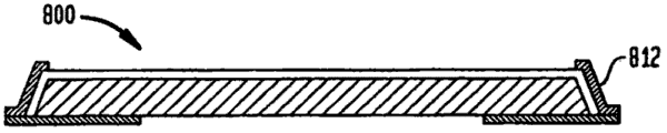
在另一实施例中,叠层中模板之间的连接可在接合步骤之后进行。图8A示出单个的微电子装置800。装置800的形成类似于图2和图7的装置。暴露于边缘804处的导电元件812不是用于为模板的另一表面提供环绕桥,而是连接元件(如粘合带、迹线或垫),以为下一个导电粘合提供表面区域。图8B示出了由装置800形成的模板叠层810的一个实施例。叠层中的每个装置都使用粘合层802连接于下一个装置。这样,各装置可能不是彼此电连接的。为导电地结合各装置,焊球或其他可流动材料806能在侧边缘附近沉积在叠层的顶部上。在施加热量时,可流动材料806向下流动以将暴露于叠层中各微电子装置边缘表面处的连接元件润湿并接合在一起。作为模板叠层组件810最终如图8B所示。
在另一实施例中,上述制造方法(图1A-1I)能同时施加到两个或更多个基板上,将它们结合在一起形成具有整体堆叠的模板的微电子装置。一个示例性的工艺流程图如图9所示。在此实施例中,两个或更多个基板能在增加侧面导电元件之前在后表面处被接合。为此,基板被构图有第一金属化层并被连接到临时载体晶片。该基板通过研磨、抛光或其他一些方法被变薄。该工艺的结果如图10A所示,类似于图1F的结构117。在图10B 中,第二结构117被上下翻转且用粘合层1002连接于第一结构117。图10C示出去除了上临时载体晶片和上粘合层之后的中间晶片叠层1000。接下来,如图10D所示,穿过基板和中央粘合层1002切割或蚀刻通道1004以暴露下基板的第一金属化层。
在本实施例中,因为基板的变薄表面朝中央粘合层面向内,独立的钝化步骤不是必需的。但是,因为在通道内可能有基板的未保护区域(这取决于通道是如何形成的),在形成通道后钝化步骤可被添加为可选步骤。图10E示出金属化层被沉积和构图从而在边缘表面处形成侧面导电元件1012后的晶片结构1010,该导电元件将每个装置1020的第一表面1001上的导体如迹线、连接垫连接于装置的第二表面1003上的导电元件。要注意,在第三金属化层形成将叠层的顶部连接于底部的侧面导电元件1012的同时,它也与上基板的被构图金属化层重叠以形成各金属化层之间的导电路径。虽然这些金属层有些重叠,但使用该方法整个工艺可被简化且实现成本节约,因为相同的结构可被用作工艺的一部分。在虚线处分离后,形成中间模板叠层装置1020且如图10F所示。类似于前述实施例,可使用如参照图4B、7或8A-C的上述方法将模板叠层装置1020接合于复合叠层1030中的其它类似装置。虽然装置1020被称为中间模板叠层装置,可以想到该装置可被封装和独自使用而不进行接下来的堆叠。
在一个变型中,可省略上基板上的第一金属化层。这样的一个示例是图10H所示的结构1040。在该变型中,用粘合层将结构1040接合于下基板,且随之形成通道1004。金属化层的沉积和接下来的构图将导致结构的外观和功能与图10E的结构1010基本相同,接着结构可以相同方式被加工和进一步堆叠。该变型中的两个晶片基板可被形成的略微不同,取消工艺中所需的金属化步骤之一。
在本实施例的另一变型中,此时没有附图,第二晶片叠层1000可被翻转且用另一粘合层连接于第一晶片叠层1000,接着再次去除上载体晶片。接着可切割和金属化该组件以形成四级连接的被堆叠装置。
在又一实施例中,可在将两个基板电连接之前以表面朝下的方式加工它们。图11A示出将被连接的两个晶片结构,它们与图1C所示的结构111和图1F所示的结构117基本相同。不是将结构111连接于将被变薄的临时 载体晶片(如图1E所示),而是直接将其连接于结构117的背面。这如图11B所示,其中两个结构都连接有粘合层1102。图11C示出上基板变薄的结果。之后,如图11D所示穿过基板和中央金属化层形成通道。在图11E中,第三金属化层被沉积和构图以形成结构1110。此时注意,第三金属化层的边缘导电元件部分1112与其它金属化层都接触。最后,去除下载体并且装置1120如图11F所示被分离。这些装置可被堆叠为如图11G所示的模板叠层组件1130或其它样式。
虽然已经参照特定实施例描述了本发明,要了解这些实施例仅为对本发明原理和应用的示例。因此要理解,在不脱离所附权利要求限定的本发明的精神和范围的情况下可对示例性实施例做出多种改进并且可设计出其它结构。
Claims (27)
1.一种微电子组件,包括:
第一微电子装置和第二微电子装置,每个微电子装置都包括带有至少一个半导体模板的模板结构,并且
每个微电子装置具有第一表面、与该第一表面相反的第二表面和以除直角外的角度远离第一和第二表面延伸的至少一个边缘表面,以及至少一个第一导电元件,其沿第一表面延伸至所述至少一个边缘表面之上并接触至少一个第二导电元件,所述至少一个第二导电元件沿所述第二表面延伸,该第一微电子装置的所述第一或第二导电元件中的至少一个被导电地结合于该第二微电子装置的所述第一或第二导电元件中的至少一个从而在其间提供导电路径。
2.如权利要求1所述的微电子组件,其特征在于,每个微电子装置的所述至少一个第一导电元件包括通过在其第一表面和所述至少一个边缘表面上镀覆而形成的第一元件,并且每个微电子装置的所述至少一个第二导电元件包括通过在其第二表面之上镀覆而形成的第二元件,其中每个微电子装置的第一元件被镀覆在其第二元件的一部分上。
3.如权利要求2所述的微电子组件,其特征在于,每个微电子装置的第一元件沿其第二元件的被第一元件在其上镀覆的部分延伸。
4.如权利要求2所述的微电子组件,其特征在于,每个微电子装置的第一元件沿其第二元件的边缘延伸。
5.如权利要求1所述的微电子组件,其特征在于,第一微电子装置的所述至少一个导电元件使用可熔性金属被导电地结合至第二微电子装置的所述至少一个导电元件。
6.如权利要求1所述的微电子组件,其特征在于,第一微电子装置的所述至少一个导电元件使用导电膏被导电地结合至第二微电子装置的所述至少一个导电元件。
7.如权利要求1所述的微电子组件,其特征在于,第一微电子装置的第一和第二表面之一面对第二微电子装置的第一和第二表面之一并且导电元件的暴露于相面对表面处的部分被结合在一起。
8.如权利要求7所述的微电子组件,其特征在于,第一和第二微电子装置的所述第一或第二导电元件中的至少一个包括分别暴露于每个微电子装置的第一或第二表面处的导电垫,所述导电垫被结合在一起。
9.如权利要求7所述的微电子组件,其特征在于,第一或第二微电子装置中至少一个的第一或第二导电元件中的至少一个包括迹线和导电垫,其中至少一个导电垫被设置为与所述至少一个微电子装置的所述至少一个边缘表面隔开一段距离。
10.如权利要求7所述的微电子组件,其特征在于,每个微电子装置的导电元件的至少一个包括紧邻其所述至少一个边缘表面的导电垫。
11.如权利要求10所述的微电子组件,其特征在于,每个微电子装置的导电垫延伸至其所述至少一个边缘表面。
12.如权利要求1所述的微电子组件,其特征在于,至少一个所述模板结构包括多个半导体模板。
13.如权利要求12所述的微电子组件,其特征在于,包括在所述至少一个模板结构内的至少两个半导体模板的结合垫-承载表面面朝着同一方向。
14.如权利要求12所述的微电子组件,其特征在于,包括在所述至少一个模板结构内的至少两个半导体模板的结合垫-承载表面面朝着不同方向。
15.如权利要求1所述的微电子组件,其特征在于,第一或第二微电子装置中至少一个的所述边缘表面相对于其第一和第二表面中至少之一以50~89度角延伸。
16.如权利要求1所述的微电子组件,其特征在于,第一和第二微电子装置以竖直方向被堆叠并且第一和第二微电子装置的所述至少一个边缘表面以离开竖直方向的方向彼此偏移。
17.如权利要求1所述的微电子组件,其特征在于,第一和第二微电子装置的第一表面侧向延伸且在侧向上具有第一尺寸,其中第一和第二微电子装置的第一表面的侧向尺寸是不同的。
18.一种微电子组件,包括:
第一微电子装置和第二微电子装置,每个微电子装置都包括带有至少一个半导体模板的模板结构,并且
每个微电子装置具有第一表面、与该第一表面相反的第二表面和以除直角外的角度延伸离开第一表面的至少一个边缘表面,以及至少一个第一导电元件,其沿第一表面延伸至所述至少一个边缘表面上并接触至少一个第二导电元件,所述至少一个第二导电元件沿第二表面延伸,该第一微电子装置的第一和第二导电元件中的至少一个被导电地结合于该第二微电子装置的第一或第二导电元件中的至少一个从而在其间提供导电路径。
19.如权利要求18所述的微电子组件,其特征在于,所述至少一个边缘表面以除直角外的角度延伸离开第一和第二表面。
20.如权利要求18所述的微电子组件,其特征在于,导电元件的暴露于第一微电子装置的所述至少一个边缘表面处的至少边缘部分被导电地结合至导电元件的暴露于第二微电子装置的所述至少一个边缘表面处的至少边缘部分以提供该导电路径。
21.如权利要求20所述的微电子组件,其特征在于,第一微电子装置的导电元件的所述至少边缘部分使用可熔性金属被导电地结合至第二微电子装置的导电元件的所述至少边缘部分。
22.如权利要求20所述的微电子组件,其特征在于,第一微电子装置的导电元件的所述至少边缘部分使用导电膏被导电地结合至第二微电子装置的导电元件的所述至少边缘部分。
23.一种制造堆叠的微电子组件的方法,包括:
将第一微电子装置的主表面设置为与第二微电子装置的主表面相对并且将暴露于第一微电子装置的主表面处的至少一个导电元件导电地结合到暴露于第二微电子装置的主表面处的至少一个导电元件以在其间提供导电路径,其中每个微电子装置包括带有至少一个半导体模板的模板结构,并且
每个微电子装置具有第一主表面、与该第一主表面相反的第二主表面、以除直角外的角度远离第一主表面延伸的至少一个边缘表面、以及至少一个导电元件,其沿第一表面延伸至所述边缘表面的至少之一之上并在第二主表面处接触所述至少一个第二导电元件,所述至少一个第二导电元件沿第二主表面延伸。
24.一种制造堆叠的微电子组件的方法,包括:
形成包括第一微电子装置和第二微电子装置的叠层,每个微电子装置都包括带有至少一个半导体模板的模板结构,并且每个微电子装置具有第一表面、与该第一表面相反的第二表面和以除直角外的角度延伸离开第一表面的至少一个边缘表面,以及至少一个第一导电元件,其沿第一表面延伸至所述边缘表面的至少之一之上并接触沿第二表面延伸的至少一个第二导电元件;并且
将暴露于第一微电子装置的边缘表面处的导电元件的至少一个的各部分导电地结合至暴露于第二微电子装置的边缘表面处的导电元件的至少一个从而在其间提供导电路径。
25.如权利要求24所述的方法,其特征在于,第一微电子装置被置于第二微电子装置之上,并且通过加热暴露于第一微电子装置的所述至少一个边缘表面处的导电元件附近的可熔性金属来进行结合步骤,这样可熔性金属流至暴露于第二微电子装置的所述至少一个边缘表面处的导电元件上。
26.如权利要求25所述的方法,其特征在于,可熔性金属桥接第一和第二微电子装置的各导电元件之间的间隙。
27.如权利要求24所述的方法,其特征在于,第一微电子装置位于第二微电子装置之上,并且通过将可流动导电材料配送至暴露于第一微电子装置的所述至少一个边缘表面处的导电元件上来进行结合步骤,这样导电材料流至暴露于第二微电子装置的所述至少一个边缘表面处的导电元件上。
Applications Claiming Priority (3)
| Application Number | Priority Date | Filing Date | Title |
|---|---|---|---|
| US6195308P | 2008-06-16 | 2008-06-16 | |
| US61/061,953 | 2008-06-16 | ||
| PCT/US2009/003643 WO2009154761A1 (en) | 2008-06-16 | 2009-06-15 | Stacking of wafer-level chip scale packages having edge contacts |
Publications (2)
| Publication Number | Publication Date |
|---|---|
| CN102067310A CN102067310A (zh) | 2011-05-18 |
| CN102067310B true CN102067310B (zh) | 2013-08-21 |
Family
ID=40974425
Family Applications (1)
| Application Number | Title | Priority Date | Filing Date |
|---|---|---|---|
| CN2009801225230A Active CN102067310B (zh) | 2008-06-16 | 2009-06-15 | 带有边缘触头的晶片级芯片规模封装的堆叠及其制造方法 |
Country Status (7)
| Country | Link |
|---|---|
| US (1) | US8680662B2 (zh) |
| EP (1) | EP2308087B1 (zh) |
| JP (1) | JP5639052B2 (zh) |
| KR (1) | KR101655897B1 (zh) |
| CN (1) | CN102067310B (zh) |
| TW (1) | TWI425611B (zh) |
| WO (1) | WO2009154761A1 (zh) |
Families Citing this family (67)
| Publication number | Priority date | Publication date | Assignee | Title |
|---|---|---|---|---|
| US7215018B2 (en) | 2004-04-13 | 2007-05-08 | Vertical Circuits, Inc. | Stacked die BGA or LGA component assembly |
| US7901989B2 (en) | 2006-10-10 | 2011-03-08 | Tessera, Inc. | Reconstituted wafer level stacking |
| US8513789B2 (en) | 2006-10-10 | 2013-08-20 | Tessera, Inc. | Edge connect wafer level stacking with leads extending along edges |
| US7829438B2 (en) | 2006-10-10 | 2010-11-09 | Tessera, Inc. | Edge connect wafer level stacking |
| US7952195B2 (en) | 2006-12-28 | 2011-05-31 | Tessera, Inc. | Stacked packages with bridging traces |
| US8723332B2 (en) | 2007-06-11 | 2014-05-13 | Invensas Corporation | Electrically interconnected stacked die assemblies |
| KR101458538B1 (ko) | 2007-07-27 | 2014-11-07 | 테세라, 인코포레이티드 | 적층형 마이크로 전자 유닛, 및 이의 제조방법 |
| CN101861646B (zh) | 2007-08-03 | 2015-03-18 | 泰塞拉公司 | 利用再生晶圆的堆叠封装 |
| US8043895B2 (en) | 2007-08-09 | 2011-10-25 | Tessera, Inc. | Method of fabricating stacked assembly including plurality of stacked microelectronic elements |
| US8704379B2 (en) | 2007-09-10 | 2014-04-22 | Invensas Corporation | Semiconductor die mount by conformal die coating |
| CN101999167B (zh) | 2008-03-12 | 2013-07-17 | 伊文萨思公司 | 支撑安装的电互连管芯组件 |
| US9153517B2 (en) * | 2008-05-20 | 2015-10-06 | Invensas Corporation | Electrical connector between die pad and z-interconnect for stacked die assemblies |
| US7863159B2 (en) | 2008-06-19 | 2011-01-04 | Vertical Circuits, Inc. | Semiconductor die separation method |
| US8680662B2 (en) | 2008-06-16 | 2014-03-25 | Tessera, Inc. | Wafer level edge stacking |
| EP2406821A2 (en) | 2009-03-13 | 2012-01-18 | Tessera, Inc. | Stacked microelectronic assemblies having vias extending through bond pads |
| TWI570879B (zh) | 2009-06-26 | 2017-02-11 | 英維瑟斯公司 | 半導體總成及晶粒堆疊總成 |
| US8242543B2 (en) * | 2009-08-26 | 2012-08-14 | Qualcomm Incorporated | Semiconductor wafer-to-wafer bonding for dissimilar semiconductor dies and/or wafers |
| WO2011056668A2 (en) | 2009-10-27 | 2011-05-12 | Vertical Circuits, Inc. | Selective die electrical insulation additive process |
| TWI544604B (zh) | 2009-11-04 | 2016-08-01 | 英維瑟斯公司 | 具有降低應力電互連的堆疊晶粒總成 |
| US20110221053A1 (en) * | 2010-03-11 | 2011-09-15 | Qualcomm Incorporated | Pre-processing to reduce wafer level warpage |
| US8796137B2 (en) * | 2010-06-24 | 2014-08-05 | Stats Chippac, Ltd. | Semiconductor device and method of forming RDL along sloped side surface of semiconductor die for z-direction interconnect |
| US8482111B2 (en) | 2010-07-19 | 2013-07-09 | Tessera, Inc. | Stackable molded microelectronic packages |
| KR101128063B1 (ko) | 2011-05-03 | 2012-04-23 | 테세라, 인코포레이티드 | 캡슐화 층의 표면에 와이어 본드를 구비하는 패키지 적층형 어셈블리 |
| US8404520B1 (en) | 2011-10-17 | 2013-03-26 | Invensas Corporation | Package-on-package assembly with wire bond vias |
| US8946757B2 (en) | 2012-02-17 | 2015-02-03 | Invensas Corporation | Heat spreading substrate with embedded interconnects |
| US8372741B1 (en) | 2012-02-24 | 2013-02-12 | Invensas Corporation | Method for package-on-package assembly with wire bonds to encapsulation surface |
| US8835228B2 (en) | 2012-05-22 | 2014-09-16 | Invensas Corporation | Substrate-less stackable package with wire-bond interconnect |
| CN103515257A (zh) * | 2012-06-18 | 2014-01-15 | 智瑞达科技(苏州)有限公司 | 高密度半导体封装结构的封装方法 |
| US9391008B2 (en) * | 2012-07-31 | 2016-07-12 | Invensas Corporation | Reconstituted wafer-level package DRAM |
| US9502390B2 (en) | 2012-08-03 | 2016-11-22 | Invensas Corporation | BVA interposer |
| US20140306331A1 (en) * | 2013-04-11 | 2014-10-16 | Infineon Technologies Austria Ag | Chip and chip arrangement |
| US20140326856A1 (en) * | 2013-05-06 | 2014-11-06 | Omnivision Technologies, Inc. | Integrated circuit stack with low profile contacts |
| US9167710B2 (en) | 2013-08-07 | 2015-10-20 | Invensas Corporation | Embedded packaging with preformed vias |
| US9685365B2 (en) | 2013-08-08 | 2017-06-20 | Invensas Corporation | Method of forming a wire bond having a free end |
| US20150076714A1 (en) | 2013-09-16 | 2015-03-19 | Invensas Corporation | Microelectronic element with bond elements to encapsulation surface |
| US9379074B2 (en) | 2013-11-22 | 2016-06-28 | Invensas Corporation | Die stacks with one or more bond via arrays of wire bond wires and with one or more arrays of bump interconnects |
| US9263394B2 (en) | 2013-11-22 | 2016-02-16 | Invensas Corporation | Multiple bond via arrays of different wire heights on a same substrate |
| US9583456B2 (en) | 2013-11-22 | 2017-02-28 | Invensas Corporation | Multiple bond via arrays of different wire heights on a same substrate |
| US9583411B2 (en) | 2014-01-17 | 2017-02-28 | Invensas Corporation | Fine pitch BVA using reconstituted wafer with area array accessible for testing |
| US10381326B2 (en) | 2014-05-28 | 2019-08-13 | Invensas Corporation | Structure and method for integrated circuits packaging with increased density |
| US9735084B2 (en) | 2014-12-11 | 2017-08-15 | Invensas Corporation | Bond via array for thermal conductivity |
| US9888579B2 (en) | 2015-03-05 | 2018-02-06 | Invensas Corporation | Pressing of wire bond wire tips to provide bent-over tips |
| US9502372B1 (en) | 2015-04-30 | 2016-11-22 | Invensas Corporation | Wafer-level packaging using wire bond wires in place of a redistribution layer |
| US9761554B2 (en) | 2015-05-07 | 2017-09-12 | Invensas Corporation | Ball bonding metal wire bond wires to metal pads |
| US9490195B1 (en) | 2015-07-17 | 2016-11-08 | Invensas Corporation | Wafer-level flipped die stacks with leadframes or metal foil interconnects |
| US9825002B2 (en) | 2015-07-17 | 2017-11-21 | Invensas Corporation | Flipped die stack |
| US9871019B2 (en) | 2015-07-17 | 2018-01-16 | Invensas Corporation | Flipped die stack assemblies with leadframe interconnects |
| US9490222B1 (en) | 2015-10-12 | 2016-11-08 | Invensas Corporation | Wire bond wires for interference shielding |
| US10490528B2 (en) | 2015-10-12 | 2019-11-26 | Invensas Corporation | Embedded wire bond wires |
| US10332854B2 (en) | 2015-10-23 | 2019-06-25 | Invensas Corporation | Anchoring structure of fine pitch bva |
| US10181457B2 (en) | 2015-10-26 | 2019-01-15 | Invensas Corporation | Microelectronic package for wafer-level chip scale packaging with fan-out |
| US10043779B2 (en) | 2015-11-17 | 2018-08-07 | Invensas Corporation | Packaged microelectronic device for a package-on-package device |
| US9659848B1 (en) | 2015-11-18 | 2017-05-23 | Invensas Corporation | Stiffened wires for offset BVA |
| US11037904B2 (en) * | 2015-11-24 | 2021-06-15 | Taiwan Semiconductor Manufacturing Company, Ltd. | Singulation and bonding methods and structures formed thereby |
| US9508691B1 (en) | 2015-12-16 | 2016-11-29 | Invensas Corporation | Flipped die stacks with multiple rows of leadframe interconnects |
| US9984992B2 (en) | 2015-12-30 | 2018-05-29 | Invensas Corporation | Embedded wire bond wires for vertical integration with separate surface mount and wire bond mounting surfaces |
| US10566310B2 (en) | 2016-04-11 | 2020-02-18 | Invensas Corporation | Microelectronic packages having stacked die and wire bond interconnects |
| US9595511B1 (en) | 2016-05-12 | 2017-03-14 | Invensas Corporation | Microelectronic packages and assemblies with improved flyby signaling operation |
| US9728524B1 (en) | 2016-06-30 | 2017-08-08 | Invensas Corporation | Enhanced density assembly having microelectronic packages mounted at substantial angle to board |
| US9935075B2 (en) | 2016-07-29 | 2018-04-03 | Invensas Corporation | Wire bonding method and apparatus for electromagnetic interference shielding |
| US9996725B2 (en) * | 2016-11-03 | 2018-06-12 | Optiz, Inc. | Under screen sensor assembly |
| JPWO2018105201A1 (ja) * | 2016-12-08 | 2019-08-08 | 株式会社村田製作所 | 複合部品及びその実装構造 |
| US10299368B2 (en) | 2016-12-21 | 2019-05-21 | Invensas Corporation | Surface integrated waveguides and circuit structures therefor |
| DE102017109670B4 (de) * | 2017-05-05 | 2019-12-24 | Infineon Technologies Ag | Herstellungsverfahren für ein Chippackage mit Seitenwandmetallisierung |
| KR102435517B1 (ko) * | 2018-04-12 | 2022-08-22 | 에스케이하이닉스 주식회사 | 칩 스택 패키지 |
| CN110648931A (zh) * | 2019-03-26 | 2020-01-03 | Pep创新私人有限公司 | 封装方法、面板组件、晶圆封装体以及芯片封装体 |
| JP2022049485A (ja) * | 2020-09-16 | 2022-03-29 | キオクシア株式会社 | 半導体記憶装置 |
Citations (2)
| Publication number | Priority date | Publication date | Assignee | Title |
|---|---|---|---|---|
| JP2002093944A (ja) * | 2000-09-11 | 2002-03-29 | Oki Electric Ind Co Ltd | 半導体装置,半導体装置の製造方法,スタック型半導体装置及びスタック型半導体装置の製造方法 |
| TW200405581A (en) * | 2002-05-13 | 2004-04-01 | Nat Semiconductor Corp | Electrical die contact structure and fabrication method |
Family Cites Families (251)
| Publication number | Priority date | Publication date | Assignee | Title |
|---|---|---|---|---|
| US4074342A (en) * | 1974-12-20 | 1978-02-14 | International Business Machines Corporation | Electrical package for lsi devices and assembly process therefor |
| US4500905A (en) * | 1981-09-30 | 1985-02-19 | Tokyo Shibaura Denki Kabushiki Kaisha | Stacked semiconductor device with sloping sides |
| US4954875A (en) * | 1986-07-17 | 1990-09-04 | Laser Dynamics, Inc. | Semiconductor wafer array with electrically conductive compliant material |
| US4897708A (en) * | 1986-07-17 | 1990-01-30 | Laser Dynamics, Inc. | Semiconductor wafer array |
| US4765864A (en) * | 1987-07-15 | 1988-08-23 | Sri International | Etching method for producing an electrochemical cell in a crystalline substrate |
| US4842699A (en) * | 1988-05-10 | 1989-06-27 | Avantek, Inc. | Method of selective via-hole and heat sink plating using a metal mask |
| JP2876773B2 (ja) * | 1990-10-22 | 1999-03-31 | セイコーエプソン株式会社 | プログラム命令語長可変型計算装置及びデータ処理装置 |
| US5614766A (en) * | 1991-09-30 | 1997-03-25 | Rohm Co., Ltd. | Semiconductor device with stacked alternate-facing chips |
| AU4242693A (en) * | 1992-05-11 | 1993-12-13 | Nchip, Inc. | Stacked devices for multichip modules |
| US5322816A (en) * | 1993-01-19 | 1994-06-21 | Hughes Aircraft Company | Method for forming deep conductive feedthroughs |
| US5426072A (en) * | 1993-01-21 | 1995-06-20 | Hughes Aircraft Company | Process of manufacturing a three dimensional integrated circuit from stacked SOI wafers using a temporary silicon substrate |
| FR2704690B1 (fr) | 1993-04-27 | 1995-06-23 | Thomson Csf | Procédé d'encapsulation de pastilles semi-conductrices, dispositif obtenu par ce procédé et application à l'interconnexion de pastilles en trois dimensions. |
| US5343071A (en) * | 1993-04-28 | 1994-08-30 | Raytheon Company | Semiconductor structures having dual surface via holes |
| DE4314907C1 (de) * | 1993-05-05 | 1994-08-25 | Siemens Ag | Verfahren zur Herstellung von vertikal miteinander elektrisch leitend kontaktierten Halbleiterbauelementen |
| IL106892A0 (en) * | 1993-09-02 | 1993-12-28 | Pierre Badehi | Methods and apparatus for producing integrated circuit devices |
| US5412539A (en) * | 1993-10-18 | 1995-05-02 | Hughes Aircraft Company | Multichip module with a mandrel-produced interconnecting decal |
| US5424245A (en) * | 1994-01-04 | 1995-06-13 | Motorola, Inc. | Method of forming vias through two-sided substrate |
| IL108359A (en) * | 1994-01-17 | 2001-04-30 | Shellcase Ltd | Method and device for creating integrated circular devices |
| US5502333A (en) * | 1994-03-30 | 1996-03-26 | International Business Machines Corporation | Semiconductor stack structures and fabrication/sparing methods utilizing programmable spare circuit |
| US5675180A (en) * | 1994-06-23 | 1997-10-07 | Cubic Memory, Inc. | Vertical interconnect process for silicon segments |
| US6228686B1 (en) * | 1995-09-18 | 2001-05-08 | Tessera, Inc. | Method of fabricating a microelectronic assembly using sheets with gaps to define lead regions |
| IL110261A0 (en) * | 1994-07-10 | 1994-10-21 | Schellcase Ltd | Packaged integrated circuit |
| US5880010A (en) * | 1994-07-12 | 1999-03-09 | Sun Microsystems, Inc. | Ultrathin electronics |
| MY114888A (en) * | 1994-08-22 | 2003-02-28 | Ibm | Method for forming a monolithic electronic module by stacking planar arrays of integrated circuit chips |
| DE4433845A1 (de) * | 1994-09-22 | 1996-03-28 | Fraunhofer Ges Forschung | Verfahren zur Herstellung einer dreidimensionalen integrierten Schaltung |
| DE4433846C2 (de) * | 1994-09-22 | 1999-06-02 | Fraunhofer Ges Forschung | Verfahren zur Herstellung einer vertikalen integrierten Schaltungsstruktur |
| US5466634A (en) * | 1994-12-20 | 1995-11-14 | International Business Machines Corporation | Electronic modules with interconnected surface metallization layers and fabrication methods therefore |
| DE19516487C1 (de) | 1995-05-05 | 1996-07-25 | Fraunhofer Ges Forschung | Verfahren zur vertikalen Integration mikroelektronischer Systeme |
| US5814889A (en) * | 1995-06-05 | 1998-09-29 | Harris Corporation | Intergrated circuit with coaxial isolation and method |
| US5618752A (en) * | 1995-06-05 | 1997-04-08 | Harris Corporation | Method of fabrication of surface mountable integrated circuits |
| US5608264A (en) * | 1995-06-05 | 1997-03-04 | Harris Corporation | Surface mountable integrated circuit with conductive vias |
| US5646067A (en) * | 1995-06-05 | 1997-07-08 | Harris Corporation | Method of bonding wafers having vias including conductive material |
| US5682062A (en) * | 1995-06-05 | 1997-10-28 | Harris Corporation | System for interconnecting stacked integrated circuits |
| US5604673A (en) * | 1995-06-07 | 1997-02-18 | Hughes Electronics | Low temperature co-fired ceramic substrates for power converters |
| US5648684A (en) | 1995-07-26 | 1997-07-15 | International Business Machines Corporation | Endcap chip with conductive, monolithic L-connect for multichip stack |
| US6002167A (en) * | 1995-09-22 | 1999-12-14 | Hitachi Cable, Ltd. | Semiconductor device having lead on chip structure |
| JP2743904B2 (ja) * | 1996-02-16 | 1998-04-28 | 日本電気株式会社 | 半導体基板およびこれを用いた半導体装置の製造方法 |
| US5817530A (en) * | 1996-05-20 | 1998-10-06 | Micron Technology, Inc. | Use of conductive lines on the back side of wafers and dice for semiconductor interconnects |
| US6784023B2 (en) | 1996-05-20 | 2004-08-31 | Micron Technology, Inc. | Method of fabrication of stacked semiconductor devices |
| JP3620936B2 (ja) * | 1996-10-11 | 2005-02-16 | 浜松ホトニクス株式会社 | 裏面照射型受光デバイスおよびその製造方法 |
| KR100214562B1 (ko) * | 1997-03-24 | 1999-08-02 | 구본준 | 적층 반도체 칩 패키지 및 그 제조 방법 |
| US5915167A (en) * | 1997-04-04 | 1999-06-22 | Elm Technology Corporation | Three dimensional structure memory |
| US6551857B2 (en) | 1997-04-04 | 2003-04-22 | Elm Technology Corporation | Three dimensional structure integrated circuits |
| DE69737262T2 (de) | 1997-11-26 | 2007-11-08 | Stmicroelectronics S.R.L., Agrate Brianza | Herstellungsverfahren für einen Vorder-Hinterseiten-Durchkontakt in mikro-integrierten Schaltungen |
| US6620731B1 (en) | 1997-12-18 | 2003-09-16 | Micron Technology, Inc. | Method for fabricating semiconductor components and interconnects with contacts on opposing sides |
| US6624505B2 (en) * | 1998-02-06 | 2003-09-23 | Shellcase, Ltd. | Packaged integrated circuits and methods of producing thereof |
| IL123207A0 (en) | 1998-02-06 | 1998-09-24 | Shellcase Ltd | Integrated circuit device |
| JP4538107B2 (ja) * | 1998-03-02 | 2010-09-08 | エヌエックスピー ビー ヴィ | 半導体素子及び金属化層を有する絶縁層が接着剤により取付られているガラス支持体を有する半導体装置 |
| US6982475B1 (en) * | 1998-03-20 | 2006-01-03 | Mcsp, Llc | Hermetic wafer scale integrated circuit structure |
| KR100266693B1 (ko) * | 1998-05-30 | 2000-09-15 | 김영환 | 적층가능한 비지에이 반도체 칩 패키지 및 그 제조방법 |
| US6492201B1 (en) * | 1998-07-10 | 2002-12-10 | Tessera, Inc. | Forming microelectronic connection components by electrophoretic deposition |
| US6103552A (en) * | 1998-08-10 | 2000-08-15 | Lin; Mou-Shiung | Wafer scale packaging scheme |
| US6153929A (en) * | 1998-08-21 | 2000-11-28 | Micron Technology, Inc. | Low profile multi-IC package connector |
| US6261865B1 (en) * | 1998-10-06 | 2001-07-17 | Micron Technology, Inc. | Multi chip semiconductor package and method of construction |
| KR100304959B1 (ko) * | 1998-10-21 | 2001-09-24 | 김영환 | 칩 적층형 반도체 패키지 및 그 제조방법 |
| SG78324A1 (en) * | 1998-12-17 | 2001-02-20 | Eriston Technologies Pte Ltd | Bumpless flip chip assembly with strips-in-via and plating |
| US6229216B1 (en) * | 1999-01-11 | 2001-05-08 | Intel Corporation | Silicon interposer and multi-chip-module (MCM) with through substrate vias |
| JP3228257B2 (ja) * | 1999-01-22 | 2001-11-12 | 日本電気株式会社 | メモリパッケージ |
| US6130823A (en) * | 1999-02-01 | 2000-10-10 | Raytheon E-Systems, Inc. | Stackable ball grid array module and method |
| US6204562B1 (en) * | 1999-02-11 | 2001-03-20 | United Microelectronics Corp. | Wafer-level chip scale package |
| EP1041624A1 (en) * | 1999-04-02 | 2000-10-04 | Interuniversitair Microelektronica Centrum Vzw | Method of transferring ultra-thin substrates and application of the method to the manufacture of a multilayer thin film device |
| JP3532788B2 (ja) * | 1999-04-13 | 2004-05-31 | 唯知 須賀 | 半導体装置及びその製造方法 |
| US20030233704A1 (en) * | 2000-04-17 | 2003-12-25 | Miguel Castellote | Air massage system for bathtub |
| WO2000074134A1 (de) * | 1999-05-27 | 2000-12-07 | Fraunhofer-Gesellschaft zur Förderung der angewandten Forschung e.V. | Verfahren zur vertikalen integration von elektrischen bauelementen mittels rückseitenkontaktierung |
| JP2001035995A (ja) | 1999-07-22 | 2001-02-09 | Seiko Epson Corp | 半導体チップの貫通孔形成方法 |
| WO2001015228A1 (fr) | 1999-08-19 | 2001-03-01 | Seiko Epson Corporation | Panneau de cablage, procede de fabrication d'un panneau de cablage, dispositif semiconducteur, procede de fabrication d'un dispositif semiconducteur, carte a circuit imprime et appareil electronique |
| US6277669B1 (en) * | 1999-09-15 | 2001-08-21 | Industrial Technology Research Institute | Wafer level packaging method and packages formed |
| JP2001156250A (ja) | 1999-11-24 | 2001-06-08 | Seiko Epson Corp | 半導体チップ、マルチチップパッケージ,および半導体装置と、並びに、それを用いた電子機器 |
| IL133453A0 (en) | 1999-12-10 | 2001-04-30 | Shellcase Ltd | Methods for producing packaged integrated circuit devices and packaged integrated circuit devices produced thereby |
| US6376904B1 (en) * | 1999-12-23 | 2002-04-23 | Rambus Inc. | Redistributed bond pads in stacked integrated circuit die package |
| US6621155B1 (en) * | 1999-12-23 | 2003-09-16 | Rambus Inc. | Integrated circuit device having stacked dies and impedance balanced transmission lines |
| JP3879351B2 (ja) | 2000-01-27 | 2007-02-14 | セイコーエプソン株式会社 | 半導体チップの製造方法 |
| JP3684978B2 (ja) | 2000-02-03 | 2005-08-17 | セイコーエプソン株式会社 | 半導体装置およびその製造方法ならびに電子機器 |
| JP2001223323A (ja) | 2000-02-10 | 2001-08-17 | Mitsubishi Electric Corp | 半導体装置 |
| US6498387B1 (en) * | 2000-02-15 | 2002-12-24 | Wen-Ken Yang | Wafer level package and the process of the same |
| US6252305B1 (en) * | 2000-02-29 | 2001-06-26 | Advanced Semiconductor Engineering, Inc. | Multichip module having a stacked chip arrangement |
| US6344401B1 (en) * | 2000-03-09 | 2002-02-05 | Atmel Corporation | Method of forming a stacked-die integrated circuit chip package on a water level |
| US6396710B1 (en) * | 2000-05-12 | 2002-05-28 | Raytheon Company | High density interconnect module |
| JP3879816B2 (ja) | 2000-06-02 | 2007-02-14 | セイコーエプソン株式会社 | 半導体装置及びその製造方法、積層型半導体装置、回路基板並びに電子機器 |
| US6472247B1 (en) * | 2000-06-26 | 2002-10-29 | Ricoh Company, Ltd. | Solid-state imaging device and method of production of the same |
| US6693358B2 (en) * | 2000-10-23 | 2004-02-17 | Matsushita Electric Industrial Co., Ltd. | Semiconductor chip, wiring board and manufacturing process thereof as well as semiconductor device |
| JP3433193B2 (ja) | 2000-10-23 | 2003-08-04 | 松下電器産業株式会社 | 半導体チップおよびその製造方法 |
| JP4505983B2 (ja) | 2000-12-01 | 2010-07-21 | 日本電気株式会社 | 半導体装置 |
| JP3420748B2 (ja) * | 2000-12-14 | 2003-06-30 | 松下電器産業株式会社 | 半導体装置及びその製造方法 |
| JP2002184937A (ja) * | 2000-12-18 | 2002-06-28 | Shinko Electric Ind Co Ltd | 半導体装置の実装構造 |
| US20020074637A1 (en) * | 2000-12-19 | 2002-06-20 | Intel Corporation | Stacked flip chip assemblies |
| EP1356718A4 (en) | 2000-12-21 | 2009-12-02 | Tessera Tech Hungary Kft | PACKAGED INTEGRATED CIRCUITS AND METHOD FOR THE PRODUCTION THEREOF |
| JP3915513B2 (ja) | 2001-01-12 | 2007-05-16 | コニカミノルタホールディングス株式会社 | 撮像装置 |
| US20020098620A1 (en) * | 2001-01-24 | 2002-07-25 | Yi-Chuan Ding | Chip scale package and manufacturing method thereof |
| KR100352236B1 (ko) * | 2001-01-30 | 2002-09-12 | 삼성전자 주식회사 | 접지 금속층을 갖는 웨이퍼 레벨 패키지 |
| KR100895549B1 (ko) | 2001-02-08 | 2009-04-29 | 가부시키가이샤 히타치세이사쿠쇼 | 반도체 집적회로장치 및 그 제조방법 |
| KR100364635B1 (ko) * | 2001-02-09 | 2002-12-16 | 삼성전자 주식회사 | 칩-레벨에 형성된 칩 선택용 패드를 포함하는 칩-레벨3차원 멀티-칩 패키지 및 그 제조 방법 |
| US6717254B2 (en) | 2001-02-22 | 2004-04-06 | Tru-Si Technologies, Inc. | Devices having substrates with opening passing through the substrates and conductors in the openings, and methods of manufacture |
| US6498381B2 (en) | 2001-02-22 | 2002-12-24 | Tru-Si Technologies, Inc. | Semiconductor structures having multiple conductive layers in an opening, and methods for fabricating same |
| US7115986B2 (en) * | 2001-05-02 | 2006-10-03 | Micron Technology, Inc. | Flexible ball grid array chip scale packages |
| JP3651413B2 (ja) * | 2001-05-21 | 2005-05-25 | 日立電線株式会社 | 半導体装置用テープキャリア及びそれを用いた半導体装置、半導体装置用テープキャリアの製造方法及び半導体装置の製造方法 |
| US6528408B2 (en) | 2001-05-21 | 2003-03-04 | Micron Technology, Inc. | Method for bumped die and wire bonded board-on-chip package |
| US6878608B2 (en) | 2001-05-31 | 2005-04-12 | International Business Machines Corporation | Method of manufacture of silicon based package |
| US20030006494A1 (en) * | 2001-07-03 | 2003-01-09 | Lee Sang Ho | Thin profile stackable semiconductor package and method for manufacturing |
| JP3660918B2 (ja) | 2001-07-04 | 2005-06-15 | 松下電器産業株式会社 | 半導体装置及びその製造方法 |
| KR100394808B1 (ko) * | 2001-07-19 | 2003-08-14 | 삼성전자주식회사 | 웨이퍼 레벨 적층 칩 패키지 및 그 제조 방법 |
| US6787916B2 (en) * | 2001-09-13 | 2004-09-07 | Tru-Si Technologies, Inc. | Structures having a substrate with a cavity and having an integrated circuit bonded to a contact pad located in the cavity |
| US6727576B2 (en) * | 2001-10-31 | 2004-04-27 | Infineon Technologies Ag | Transfer wafer level packaging |
| US6611052B2 (en) * | 2001-11-16 | 2003-08-26 | Micron Technology, Inc. | Wafer level stackable semiconductor package |
| JP2003163324A (ja) | 2001-11-27 | 2003-06-06 | Nec Corp | ユニット半導体装置及びその製造方法並びに3次元積層型半導体装置 |
| US6607941B2 (en) * | 2002-01-11 | 2003-08-19 | National Semiconductor Corporation | Process and structure improvements to shellcase style packaging technology |
| US6743660B2 (en) * | 2002-01-12 | 2004-06-01 | Taiwan Semiconductor Manufacturing Co., Ltd | Method of making a wafer level chip scale package |
| JP4002106B2 (ja) | 2002-01-16 | 2007-10-31 | 日立オムロンターミナルソリューションズ株式会社 | 自動取引装置 |
| KR100486832B1 (ko) | 2002-02-06 | 2005-05-03 | 삼성전자주식회사 | 반도체 칩과 적층 칩 패키지 및 그 제조 방법 |
| US6806559B2 (en) | 2002-04-22 | 2004-10-19 | Irvine Sensors Corporation | Method and apparatus for connecting vertically stacked integrated circuit chips |
| TWI232560B (en) | 2002-04-23 | 2005-05-11 | Sanyo Electric Co | Semiconductor device and its manufacture |
| JP2003318178A (ja) | 2002-04-24 | 2003-11-07 | Seiko Epson Corp | 半導体装置及びその製造方法、回路基板並びに電子機器 |
| TWI229435B (en) | 2002-06-18 | 2005-03-11 | Sanyo Electric Co | Manufacture of semiconductor device |
| JP4215571B2 (ja) | 2002-06-18 | 2009-01-28 | 三洋電機株式会社 | 半導体装置の製造方法 |
| US6984545B2 (en) | 2002-07-22 | 2006-01-10 | Micron Technology, Inc. | Methods of encapsulating selected locations of a semiconductor die assembly using a thick solder mask |
| JP2004063569A (ja) | 2002-07-25 | 2004-02-26 | Seiko Epson Corp | 半導体装置及びその製造方法、回路基板並びに電子機器 |
| US6903442B2 (en) | 2002-08-29 | 2005-06-07 | Micron Technology, Inc. | Semiconductor component having backside pin contacts |
| US7329563B2 (en) | 2002-09-03 | 2008-02-12 | Industrial Technology Research Institute | Method for fabrication of wafer level package incorporating dual compliant layers |
| SE0202681D0 (sv) | 2002-09-10 | 2002-09-10 | Frank Niklaus | Hermetic sealing with combined adhesive bonding and sealing rings |
| US20040061213A1 (en) | 2002-09-17 | 2004-04-01 | Chippac, Inc. | Semiconductor multi-package module having package stacked over die-up flip chip ball grid array package and having wire bond interconnect between stacked packages |
| JP4081666B2 (ja) * | 2002-09-24 | 2008-04-30 | セイコーエプソン株式会社 | 半導体装置及びその製造方法、回路基板並びに電子機器 |
| US20040104454A1 (en) | 2002-10-10 | 2004-06-03 | Rohm Co., Ltd. | Semiconductor device and method of producing the same |
| TWI227050B (en) | 2002-10-11 | 2005-01-21 | Sanyo Electric Co | Semiconductor device and method for manufacturing the same |
| US6656827B1 (en) * | 2002-10-17 | 2003-12-02 | Taiwan Semiconductor Manufacturing Co., Ltd. | Electrical performance enhanced wafer level chip scale package with ground |
| US6869824B2 (en) | 2002-10-29 | 2005-03-22 | Ultratera Corporation | Fabrication method of window-type ball grid array semiconductor package |
| TWI227550B (en) | 2002-10-30 | 2005-02-01 | Sanyo Electric Co | Semiconductor device manufacturing method |
| JP2004153130A (ja) | 2002-10-31 | 2004-05-27 | Olympus Corp | 半導体装置及びその製造方法 |
| JP2004158536A (ja) | 2002-11-05 | 2004-06-03 | Fujitsu Ltd | 半導体装置及び半導体装置の製造方法 |
| JP4056854B2 (ja) | 2002-11-05 | 2008-03-05 | 新光電気工業株式会社 | 半導体装置の製造方法 |
| DE10253163B4 (de) | 2002-11-14 | 2015-07-23 | Epcos Ag | Bauelement mit hermetischer Verkapselung und Waferscale Verfahren zur Herstellung |
| US20050012225A1 (en) | 2002-11-15 | 2005-01-20 | Choi Seung-Yong | Wafer-level chip scale package and method for fabricating and using the same |
| WO2004055891A1 (ja) * | 2002-12-17 | 2004-07-01 | Fujitsu Limited | 半導体装置および積層型半導体装置 |
| JP3566957B2 (ja) | 2002-12-24 | 2004-09-15 | 沖電気工業株式会社 | 半導体装置及びその製造方法 |
| KR20040059742A (ko) | 2002-12-30 | 2004-07-06 | 동부전자 주식회사 | 반도체용 멀티 칩 모듈의 패키징 방법 |
| JP4145301B2 (ja) | 2003-01-15 | 2008-09-03 | 富士通株式会社 | 半導体装置及び三次元実装半導体装置 |
| JP3680839B2 (ja) | 2003-03-18 | 2005-08-10 | セイコーエプソン株式会社 | 半導体装置および半導体装置の製造方法 |
| JP3972846B2 (ja) | 2003-03-25 | 2007-09-05 | セイコーエプソン株式会社 | 半導体装置の製造方法 |
| EP1519410A1 (en) | 2003-09-25 | 2005-03-30 | Interuniversitair Microelektronica Centrum vzw ( IMEC) | Method for producing electrical through hole interconnects and devices made thereof |
| US6897148B2 (en) | 2003-04-09 | 2005-05-24 | Tru-Si Technologies, Inc. | Electroplating and electroless plating of conductive materials into openings, and structures obtained thereby |
| JP4373695B2 (ja) | 2003-04-16 | 2009-11-25 | 浜松ホトニクス株式会社 | 裏面照射型光検出装置の製造方法 |
| SG119185A1 (en) | 2003-05-06 | 2006-02-28 | Micron Technology Inc | Method for packaging circuits and packaged circuits |
| JP2004342862A (ja) | 2003-05-16 | 2004-12-02 | Sony Corp | 半導体装置及びその製造方法、疑似ウェーハ及びその製造方法、並びにマルチチップモジュール |
| EP1482553A3 (en) | 2003-05-26 | 2007-03-28 | Sanyo Electric Co., Ltd. | Semiconductor device and manufacturing method thereof |
| JP4130158B2 (ja) | 2003-06-09 | 2008-08-06 | 三洋電機株式会社 | 半導体装置の製造方法、半導体装置 |
| KR100778597B1 (ko) | 2003-06-03 | 2007-11-22 | 가시오게산키 가부시키가이샤 | 적층 반도체 장치와 그 제조방법 |
| US6972480B2 (en) | 2003-06-16 | 2005-12-06 | Shellcase Ltd. | Methods and apparatus for packaging integrated circuit devices |
| JP3646720B2 (ja) | 2003-06-19 | 2005-05-11 | セイコーエプソン株式会社 | 半導体装置及びその製造方法、回路基板並びに電子機器 |
| EP1639634B1 (en) | 2003-06-20 | 2009-04-01 | Nxp B.V. | Electronic device, assembly and methods of manufacturing an electronic device |
| WO2005004195A2 (en) | 2003-07-03 | 2005-01-13 | Shellcase Ltd. | Method and apparatus for packaging integrated circuit devices |
| JP2005045073A (ja) | 2003-07-23 | 2005-02-17 | Hamamatsu Photonics Kk | 裏面入射型光検出素子 |
| KR100537892B1 (ko) | 2003-08-26 | 2005-12-21 | 삼성전자주식회사 | 칩 스택 패키지와 그 제조 방법 |
| US7180149B2 (en) | 2003-08-28 | 2007-02-20 | Fujikura Ltd. | Semiconductor package with through-hole |
| US7061085B2 (en) | 2003-09-19 | 2006-06-13 | Micron Technology, Inc. | Semiconductor component and system having stiffener and circuit decal |
| KR100594229B1 (ko) | 2003-09-19 | 2006-07-03 | 삼성전자주식회사 | 반도체 패키지 및 그 제조방법 |
| JP2005101067A (ja) | 2003-09-22 | 2005-04-14 | Sharp Corp | 基板の配線構造および配線形成方法 |
| WO2005031862A1 (en) | 2003-09-26 | 2005-04-07 | Tessera, Inc. | Structure and method of making sealed capped chips |
| SG120123A1 (en) * | 2003-09-30 | 2006-03-28 | Micron Technology Inc | Castellated chip-scale packages and methods for fabricating the same |
| KR100621992B1 (ko) | 2003-11-19 | 2006-09-13 | 삼성전자주식회사 | 이종 소자들의 웨이퍼 레벨 적층 구조와 방법 및 이를이용한 시스템-인-패키지 |
| US7049170B2 (en) | 2003-12-17 | 2006-05-23 | Tru-Si Technologies, Inc. | Integrated circuits and packaging substrates with cavities, and attachment methods including insertion of protruding contact pads into cavities |
| US7060601B2 (en) | 2003-12-17 | 2006-06-13 | Tru-Si Technologies, Inc. | Packaging substrates for integrated circuits and soldering methods |
| US20050156330A1 (en) | 2004-01-21 | 2005-07-21 | Harris James M. | Through-wafer contact to bonding pad |
| DE102004008135A1 (de) | 2004-02-18 | 2005-09-22 | Infineon Technologies Ag | Halbleiterbauteil mit einem Stapel aus Halbleiterchips und Verfahren zur Herstellung desselben |
| US7160753B2 (en) | 2004-03-16 | 2007-01-09 | Voxtel, Inc. | Silicon-on-insulator active pixel sensors |
| US7215018B2 (en) | 2004-04-13 | 2007-05-08 | Vertical Circuits, Inc. | Stacked die BGA or LGA component assembly |
| JP4285309B2 (ja) | 2004-04-13 | 2009-06-24 | パナソニック株式会社 | 電子回路モジュールの製造方法と多層電子回路モジュールおよびその製造方法 |
| US7952189B2 (en) | 2004-05-27 | 2011-05-31 | Chang-Feng Wan | Hermetic packaging and method of manufacture and use therefore |
| US7232754B2 (en) | 2004-06-29 | 2007-06-19 | Micron Technology, Inc. | Microelectronic devices and methods for forming interconnects in microelectronic devices |
| JP4211696B2 (ja) | 2004-06-30 | 2009-01-21 | ソニー株式会社 | 固体撮像装置の製造方法 |
| KR100587081B1 (ko) | 2004-06-30 | 2006-06-08 | 주식회사 하이닉스반도체 | 개선된 열방출 특성을 갖는 반도체 패키지 |
| KR100605314B1 (ko) | 2004-07-22 | 2006-07-28 | 삼성전자주식회사 | 재배선 보호 피막을 가지는 웨이퍼 레벨 패키지의 제조 방법 |
| DE102004039906A1 (de) | 2004-08-18 | 2005-08-18 | Infineon Technologies Ag | Verfahren zur Herstellung eines elektronischen Bauelements sowie ein elektronisches Bauelement mit mindestens zwei integrierten Bausteinen |
| US20060043556A1 (en) | 2004-08-25 | 2006-03-02 | Chao-Yuan Su | Stacked packaging methods and structures |
| US7378342B2 (en) | 2004-08-27 | 2008-05-27 | Micron Technology, Inc. | Methods for forming vias varying lateral dimensions |
| US7129567B2 (en) | 2004-08-31 | 2006-10-31 | Micron Technology, Inc. | Substrate, semiconductor die, multichip module, and system including a via structure comprising a plurality of conductive elements |
| KR100604049B1 (ko) | 2004-09-01 | 2006-07-24 | 동부일렉트로닉스 주식회사 | 반도체 칩 패키지 및 그 제조방법 |
| JP2006073825A (ja) | 2004-09-02 | 2006-03-16 | Toshiba Corp | 半導体装置及びその実装方法 |
| WO2006027981A1 (ja) | 2004-09-08 | 2006-03-16 | Matsushita Electric Industrial Co., Ltd. | 立体的電子回路装置とそれを用いた電子機器およびその製造方法 |
| TWI288448B (en) | 2004-09-10 | 2007-10-11 | Toshiba Corp | Semiconductor device and method of manufacturing the same |
| JP4139803B2 (ja) | 2004-09-28 | 2008-08-27 | シャープ株式会社 | 半導体装置の製造方法 |
| KR100855819B1 (ko) | 2004-10-08 | 2008-09-01 | 삼성전기주식회사 | 금속 밀봉부재가 형성된 mems 패키지 |
| KR100676493B1 (ko) | 2004-10-08 | 2007-02-01 | 디엔제이 클럽 인코 | 재배선 기판을 이용한 웨이퍼 레벨 칩 스케일 패키지의제조 방법 |
| JP4873517B2 (ja) | 2004-10-28 | 2012-02-08 | オンセミコンダクター・トレーディング・リミテッド | 半導体装置及びその製造方法 |
| DE102004052921A1 (de) * | 2004-10-29 | 2006-05-11 | Infineon Technologies Ag | Verfahren zur Herstellung von Halbleiterbauelementen mit externen Kontaktierungen |
| FR2879347A1 (fr) | 2004-12-14 | 2006-06-16 | Commissariat Energie Atomique | Dispositif electronique a deux composants assembles et procede de fabrication d'un tel dispositif |
| US20060138626A1 (en) | 2004-12-29 | 2006-06-29 | Tessera, Inc. | Microelectronic packages using a ceramic substrate having a window and a conductive surface region |
| KR20060087273A (ko) | 2005-01-28 | 2006-08-02 | 삼성전기주식회사 | 반도체 패키지및 그 제조방법 |
| US7675153B2 (en) | 2005-02-02 | 2010-03-09 | Kabushiki Kaisha Toshiba | Semiconductor device having semiconductor chips stacked and mounted thereon and manufacturing method thereof |
| US7538032B2 (en) | 2005-06-23 | 2009-05-26 | Teledyne Scientific & Imaging, Llc | Low temperature method for fabricating high-aspect ratio vias and devices fabricated by said method |
| US7449779B2 (en) | 2005-03-22 | 2008-11-11 | Tessera, Inc. | Wire bonded wafer level cavity package |
| US7326592B2 (en) | 2005-04-04 | 2008-02-05 | Infineon Technologies Ag | Stacked die package |
| JP4237160B2 (ja) | 2005-04-08 | 2009-03-11 | エルピーダメモリ株式会社 | 積層型半導体装置 |
| JP4308797B2 (ja) | 2005-05-02 | 2009-08-05 | 株式会社アドバンストシステムズジャパン | 半導体パッケージおよびソケット付き回路基板 |
| US7208345B2 (en) | 2005-05-11 | 2007-04-24 | Infineon Technologies Ag | Method of manufacturing a semiconductor device comprising stacked chips and a corresponding semiconductor device |
| JP2007019107A (ja) | 2005-07-05 | 2007-01-25 | Shinko Electric Ind Co Ltd | 半導体装置および半導体装置の製造方法 |
| KR100629498B1 (ko) | 2005-07-15 | 2006-09-28 | 삼성전자주식회사 | 마이크로 패키지, 멀티―스택 마이크로 패키지 및 이들의제조방법 |
| JP4551321B2 (ja) | 2005-07-21 | 2010-09-29 | 新光電気工業株式会社 | 電子部品実装構造及びその製造方法 |
| US7485968B2 (en) | 2005-08-11 | 2009-02-03 | Ziptronix, Inc. | 3D IC method and device |
| US7419853B2 (en) | 2005-08-11 | 2008-09-02 | Hymite A/S | Method of fabrication for chip scale package for a micro component |
| SG130066A1 (en) | 2005-08-26 | 2007-03-20 | Micron Technology Inc | Microelectronic device packages, stacked microelectronic device packages, and methods for manufacturing microelectronic devices |
| US7485969B2 (en) | 2005-09-01 | 2009-02-03 | Micron Technology, Inc. | Stacked microelectronic devices and methods for manufacturing microelectronic devices |
| US20070052050A1 (en) | 2005-09-07 | 2007-03-08 | Bart Dierickx | Backside thinned image sensor with integrated lens stack |
| KR20070048952A (ko) | 2005-11-07 | 2007-05-10 | 삼성전자주식회사 | 내부 접속 단자를 갖는 멀티 칩 패키지 |
| US20070126085A1 (en) | 2005-12-02 | 2007-06-07 | Nec Electronics Corporation | Semiconductor device and method of manufacturing the same |
| WO2007066409A1 (ja) | 2005-12-09 | 2007-06-14 | Spansion Llc | 半導体装置およびその製造方法 |
| US7981726B2 (en) | 2005-12-12 | 2011-07-19 | Intel Corporation | Copper plating connection for multi-die stack in substrate package |
| US7632708B2 (en) | 2005-12-27 | 2009-12-15 | Tessera, Inc. | Microelectronic component with photo-imageable substrate |
| US20070158807A1 (en) * | 2005-12-29 | 2007-07-12 | Daoqiang Lu | Edge interconnects for die stacking |
| US20070190747A1 (en) | 2006-01-23 | 2007-08-16 | Tessera Technologies Hungary Kft. | Wafer level packaging to lidded chips |
| SG135074A1 (en) | 2006-02-28 | 2007-09-28 | Micron Technology Inc | Microelectronic devices, stacked microelectronic devices, and methods for manufacturing such devices |
| US7741707B2 (en) | 2006-02-27 | 2010-06-22 | Stats Chippac Ltd. | Stackable integrated circuit package system |
| US7510928B2 (en) | 2006-05-05 | 2009-03-31 | Tru-Si Technologies, Inc. | Dielectric trenches, nickel/tantalum oxide structures, and chemical mechanical polishing techniques |
| WO2008018524A1 (en) | 2006-08-11 | 2008-02-14 | Sanyo Electric Co., Ltd. | Semiconductor device and its manufacturing method |
| US7888185B2 (en) | 2006-08-17 | 2011-02-15 | Micron Technology, Inc. | Semiconductor device assemblies and systems including at least one conductive pathway extending around a side of at least one semiconductor device |
| US7531445B2 (en) | 2006-09-26 | 2009-05-12 | Hymite A/S | Formation of through-wafer electrical interconnections and other structures using a thin dielectric membrane |
| US7901989B2 (en) | 2006-10-10 | 2011-03-08 | Tessera, Inc. | Reconstituted wafer level stacking |
| US8513789B2 (en) | 2006-10-10 | 2013-08-20 | Tessera, Inc. | Edge connect wafer level stacking with leads extending along edges |
| US7829438B2 (en) | 2006-10-10 | 2010-11-09 | Tessera, Inc. | Edge connect wafer level stacking |
| US7759166B2 (en) | 2006-10-17 | 2010-07-20 | Tessera, Inc. | Microelectronic packages fabricated at the wafer level and methods therefor |
| US7935568B2 (en) | 2006-10-31 | 2011-05-03 | Tessera Technologies Ireland Limited | Wafer-level fabrication of lidded chips with electrodeposited dielectric coating |
| US7807508B2 (en) | 2006-10-31 | 2010-10-05 | Tessera Technologies Hungary Kft. | Wafer-level fabrication of lidded chips with electrodeposited dielectric coating |
| US7394152B2 (en) | 2006-11-13 | 2008-07-01 | China Wafer Level Csp Ltd. | Wafer level chip size packaged chip device with an N-shape junction inside and method of fabricating the same |
| US7663213B2 (en) | 2006-11-13 | 2010-02-16 | China Wafer Level Csp Ltd. | Wafer level chip size packaged chip device with a double-layer lead structure and method of fabricating the same |
| US8569876B2 (en) | 2006-11-22 | 2013-10-29 | Tessera, Inc. | Packaged semiconductor chips with array |
| US7791199B2 (en) | 2006-11-22 | 2010-09-07 | Tessera, Inc. | Packaged semiconductor chips |
| US7952195B2 (en) | 2006-12-28 | 2011-05-31 | Tessera, Inc. | Stacked packages with bridging traces |
| US20080157327A1 (en) | 2007-01-03 | 2008-07-03 | Advanced Chip Engineering Technology Inc. | Package on package structure for semiconductor devices and method of the same |
| JP5584474B2 (ja) | 2007-03-05 | 2014-09-03 | インヴェンサス・コーポレイション | 貫通ビアによって前面接点に接続された後面接点を有するチップ |
| US20080284041A1 (en) | 2007-05-18 | 2008-11-20 | Samsung Electronics Co., Ltd. | Semiconductor package with through silicon via and related method of fabrication |
| KR100914977B1 (ko) | 2007-06-18 | 2009-09-02 | 주식회사 하이닉스반도체 | 스택 패키지의 제조 방법 |
| WO2008157779A2 (en) | 2007-06-20 | 2008-12-24 | Vertical Circuits, Inc. | Three-dimensional circuitry formed on integrated circuit device using two- dimensional fabrication |
| US20110024890A1 (en) | 2007-06-29 | 2011-02-03 | Stats Chippac, Ltd. | Stackable Package By Using Internal Stacking Modules |
| US8766910B2 (en) | 2007-07-04 | 2014-07-01 | Cypress Semiconductor Corporation | Capacitive sensing control knob |
| JP2009032929A (ja) | 2007-07-27 | 2009-02-12 | Sanyo Electric Co Ltd | 半導体装置及びその製造方法 |
| KR101458538B1 (ko) | 2007-07-27 | 2014-11-07 | 테세라, 인코포레이티드 | 적층형 마이크로 전자 유닛, 및 이의 제조방법 |
| KR101538648B1 (ko) | 2007-07-31 | 2015-07-22 | 인벤사스 코포레이션 | 실리콘 쓰루 비아를 사용하는 반도체 패키지 공정 |
| KR101387701B1 (ko) | 2007-08-01 | 2014-04-23 | 삼성전자주식회사 | 반도체 패키지 및 이의 제조방법 |
| CN101861646B (zh) | 2007-08-03 | 2015-03-18 | 泰塞拉公司 | 利用再生晶圆的堆叠封装 |
| US8043895B2 (en) | 2007-08-09 | 2011-10-25 | Tessera, Inc. | Method of fabricating stacked assembly including plurality of stacked microelectronic elements |
| WO2009023462A1 (en) | 2007-08-10 | 2009-02-19 | Spansion Llc | Semiconductor device and method for manufacturing thereof |
| KR100905784B1 (ko) | 2007-08-16 | 2009-07-02 | 주식회사 하이닉스반도체 | 반도체 패키지용 관통 전극 및 이를 갖는 반도체 패키지 |
| KR20090047776A (ko) | 2007-11-08 | 2009-05-13 | 삼성전자주식회사 | 반도체 소자 및 그 형성 방법 |
| KR101465948B1 (ko) | 2007-12-27 | 2014-12-10 | 삼성전자주식회사 | 웨이퍼 레벨 스택 패키지 및 웨이퍼 레벨 스택 패키지 제조방법 |
| US8084854B2 (en) | 2007-12-28 | 2011-12-27 | Micron Technology, Inc. | Pass-through 3D interconnect for microelectronic dies and associated systems and methods |
| US20100053407A1 (en) | 2008-02-26 | 2010-03-04 | Tessera, Inc. | Wafer level compliant packages for rear-face illuminated solid state image sensors |
| US20090212381A1 (en) | 2008-02-26 | 2009-08-27 | Tessera, Inc. | Wafer level packages for rear-face illuminated solid state image sensors |
| US7973416B2 (en) | 2008-05-12 | 2011-07-05 | Texas Instruments Incorporated | Thru silicon enabled die stacking scheme |
| US7863721B2 (en) | 2008-06-11 | 2011-01-04 | Stats Chippac, Ltd. | Method and apparatus for wafer level integration using tapered vias |
| US8680662B2 (en) | 2008-06-16 | 2014-03-25 | Tessera, Inc. | Wafer level edge stacking |
| US20100065949A1 (en) | 2008-09-17 | 2010-03-18 | Andreas Thies | Stacked Semiconductor Chips with Through Substrate Vias |
| KR100990943B1 (ko) | 2008-11-07 | 2010-11-01 | 주식회사 하이닉스반도체 | 반도체 패키지 |
| EP2406821A2 (en) | 2009-03-13 | 2012-01-18 | Tessera, Inc. | Stacked microelectronic assemblies having vias extending through bond pads |
-
2009
- 2009-06-15 US US12/456,349 patent/US8680662B2/en active Active
- 2009-06-15 CN CN2009801225230A patent/CN102067310B/zh active Active
- 2009-06-15 KR KR1020107028161A patent/KR101655897B1/ko active IP Right Grant
- 2009-06-15 EP EP09767074.9A patent/EP2308087B1/en active Active
- 2009-06-15 JP JP2011514614A patent/JP5639052B2/ja active Active
- 2009-06-15 WO PCT/US2009/003643 patent/WO2009154761A1/en active Application Filing
- 2009-06-16 TW TW098120145A patent/TWI425611B/zh not_active IP Right Cessation
Patent Citations (2)
| Publication number | Priority date | Publication date | Assignee | Title |
|---|---|---|---|---|
| JP2002093944A (ja) * | 2000-09-11 | 2002-03-29 | Oki Electric Ind Co Ltd | 半導体装置,半導体装置の製造方法,スタック型半導体装置及びスタック型半導体装置の製造方法 |
| TW200405581A (en) * | 2002-05-13 | 2004-04-01 | Nat Semiconductor Corp | Electrical die contact structure and fabrication method |
Also Published As
| Publication number | Publication date |
|---|---|
| EP2308087B1 (en) | 2020-08-12 |
| TW201005918A (en) | 2010-02-01 |
| JP5639052B2 (ja) | 2014-12-10 |
| WO2009154761A9 (en) | 2010-03-11 |
| TWI425611B (zh) | 2014-02-01 |
| EP2308087A1 (en) | 2011-04-13 |
| US20090316378A1 (en) | 2009-12-24 |
| WO2009154761A1 (en) | 2009-12-23 |
| KR101655897B1 (ko) | 2016-09-08 |
| JP2011524647A (ja) | 2011-09-01 |
| CN102067310A (zh) | 2011-05-18 |
| KR20110027690A (ko) | 2011-03-16 |
| US8680662B2 (en) | 2014-03-25 |
Similar Documents
| Publication | Publication Date | Title |
|---|---|---|
| CN102067310B (zh) | 带有边缘触头的晶片级芯片规模封装的堆叠及其制造方法 | |
| CN105374693B (zh) | 半导体封装件及其形成方法 | |
| US7872343B1 (en) | Dual laminate package structure with embedded elements | |
| CN100479135C (zh) | 半导体器件及其制造方法 | |
| US9553076B2 (en) | Stackable molded microelectronic packages with area array unit connectors | |
| CN104882416B (zh) | 具有堆叠式封装能力的半导体封装件及其制作方法 | |
| CN107808878A (zh) | 堆叠型芯片封装结构 | |
| US7829990B1 (en) | Stackable semiconductor package including laminate interposer | |
| CN109841606A (zh) | 封装结构及其制造方法 | |
| TW201131696A (en) | Integrated circuit packaging system with stacking interconnect and method of manufacture thereof | |
| EP1109219A2 (en) | Semiconductor device having a wiring layer | |
| US20020094608A1 (en) | Semiconductor assembly without adhesive fillets | |
| US11670600B2 (en) | Panel level metal wall grids array for integrated circuit packaging | |
| CN219226269U (zh) | 电子器件 | |
| US11616017B2 (en) | Integrated circuit package structure, integrated circuit package unit and associated packaging method | |
| CN114496810A (zh) | 模块化堆栈式半导体封装方法 | |
| CN115064488B (zh) | 一种芯片互连封装结构及其制备方法 | |
| US11824001B2 (en) | Integrated circuit package structure and integrated circuit package unit | |
| JPS63204635A (ja) | メモリ−モジユ−ル | |
| CN116344506A (zh) | 封装结构及形成方法 |
Legal Events
| Date | Code | Title | Description |
|---|---|---|---|
| C06 | Publication | ||
| PB01 | Publication | ||
| C10 | Entry into substantive examination | ||
| SE01 | Entry into force of request for substantive examination | ||
| ASS | Succession or assignment of patent right |
Owner name: TESSERA INC. Free format text: FORMER OWNER: TESSERA RESEARCH, LLC Effective date: 20111111 |
|
| C41 | Transfer of patent application or patent right or utility model | ||
| TA01 | Transfer of patent application right |
Effective date of registration: 20111111 Address after: American California Applicant after: Tessera Inc. Address before: American California Applicant before: Tessera Res LLC |
|
| C14 | Grant of patent or utility model | ||
| GR01 | Patent grant |