CN102844859A - Dual carrier for joining ic die or wafers to tsv wafers - Google Patents
Dual carrier for joining ic die or wafers to tsv wafers Download PDFInfo
- Publication number
- CN102844859A CN102844859A CN2010800658302A CN201080065830A CN102844859A CN 102844859 A CN102844859 A CN 102844859A CN 2010800658302 A CN2010800658302 A CN 2010800658302A CN 201080065830 A CN201080065830 A CN 201080065830A CN 102844859 A CN102844859 A CN 102844859A
- Authority
- CN
- China
- Prior art keywords
- tsv
- wafer
- crystal grain
- attenuation
- pile
- Prior art date
- Legal status (The legal status is an assumption and is not a legal conclusion. Google has not performed a legal analysis and makes no representation as to the accuracy of the status listed.)
- Pending
Links
Images


Classifications
-
- H—ELECTRICITY
- H01—ELECTRIC ELEMENTS
- H01L—SEMICONDUCTOR DEVICES NOT COVERED BY CLASS H10
- H01L21/00—Processes or apparatus adapted for the manufacture or treatment of semiconductor or solid state devices or of parts thereof
- H01L21/67—Apparatus specially adapted for handling semiconductor or electric solid state devices during manufacture or treatment thereof; Apparatus specially adapted for handling wafers during manufacture or treatment of semiconductor or electric solid state devices or components ; Apparatus not specifically provided for elsewhere
- H01L21/683—Apparatus specially adapted for handling semiconductor or electric solid state devices during manufacture or treatment thereof; Apparatus specially adapted for handling wafers during manufacture or treatment of semiconductor or electric solid state devices or components ; Apparatus not specifically provided for elsewhere for supporting or gripping
- H01L21/6835—Apparatus specially adapted for handling semiconductor or electric solid state devices during manufacture or treatment thereof; Apparatus specially adapted for handling wafers during manufacture or treatment of semiconductor or electric solid state devices or components ; Apparatus not specifically provided for elsewhere for supporting or gripping using temporarily an auxiliary support
- H01L21/6836—Wafer tapes, e.g. grinding or dicing support tapes
-
- C—CHEMISTRY; METALLURGY
- C09—DYES; PAINTS; POLISHES; NATURAL RESINS; ADHESIVES; COMPOSITIONS NOT OTHERWISE PROVIDED FOR; APPLICATIONS OF MATERIALS NOT OTHERWISE PROVIDED FOR
- C09J—ADHESIVES; NON-MECHANICAL ASPECTS OF ADHESIVE PROCESSES IN GENERAL; ADHESIVE PROCESSES NOT PROVIDED FOR ELSEWHERE; USE OF MATERIALS AS ADHESIVES
- C09J5/00—Adhesive processes in general; Adhesive processes not provided for elsewhere, e.g. relating to primers
- C09J5/06—Adhesive processes in general; Adhesive processes not provided for elsewhere, e.g. relating to primers involving heating of the applied adhesive
-
- H—ELECTRICITY
- H01—ELECTRIC ELEMENTS
- H01L—SEMICONDUCTOR DEVICES NOT COVERED BY CLASS H10
- H01L21/00—Processes or apparatus adapted for the manufacture or treatment of semiconductor or solid state devices or of parts thereof
- H01L21/70—Manufacture or treatment of devices consisting of a plurality of solid state components formed in or on a common substrate or of parts thereof; Manufacture of integrated circuit devices or of parts thereof
- H01L21/71—Manufacture of specific parts of devices defined in group H01L21/70
- H01L21/768—Applying interconnections to be used for carrying current between separate components within a device comprising conductors and dielectrics
- H01L21/76898—Applying interconnections to be used for carrying current between separate components within a device comprising conductors and dielectrics formed through a semiconductor substrate
-
- H—ELECTRICITY
- H01—ELECTRIC ELEMENTS
- H01L—SEMICONDUCTOR DEVICES NOT COVERED BY CLASS H10
- H01L24/00—Arrangements for connecting or disconnecting semiconductor or solid-state bodies; Methods or apparatus related thereto
- H01L24/80—Methods for connecting semiconductor or other solid state bodies using means for bonding being attached to, or being formed on, the surface to be connected
- H01L24/81—Methods for connecting semiconductor or other solid state bodies using means for bonding being attached to, or being formed on, the surface to be connected using a bump connector
-
- H—ELECTRICITY
- H01—ELECTRIC ELEMENTS
- H01L—SEMICONDUCTOR DEVICES NOT COVERED BY CLASS H10
- H01L24/00—Arrangements for connecting or disconnecting semiconductor or solid-state bodies; Methods or apparatus related thereto
- H01L24/93—Batch processes
- H01L24/94—Batch processes at wafer-level, i.e. with connecting carried out on a wafer comprising a plurality of undiced individual devices
-
- H—ELECTRICITY
- H01—ELECTRIC ELEMENTS
- H01L—SEMICONDUCTOR DEVICES NOT COVERED BY CLASS H10
- H01L24/00—Arrangements for connecting or disconnecting semiconductor or solid-state bodies; Methods or apparatus related thereto
- H01L24/93—Batch processes
- H01L24/95—Batch processes at chip-level, i.e. with connecting carried out on a plurality of singulated devices, i.e. on diced chips
- H01L24/97—Batch processes at chip-level, i.e. with connecting carried out on a plurality of singulated devices, i.e. on diced chips the devices being connected to a common substrate, e.g. interposer, said common substrate being separable into individual assemblies after connecting
-
- H—ELECTRICITY
- H01—ELECTRIC ELEMENTS
- H01L—SEMICONDUCTOR DEVICES NOT COVERED BY CLASS H10
- H01L25/00—Assemblies consisting of a plurality of individual semiconductor or other solid state devices ; Multistep manufacturing processes thereof
- H01L25/03—Assemblies consisting of a plurality of individual semiconductor or other solid state devices ; Multistep manufacturing processes thereof all the devices being of a type provided for in the same subgroup of groups H01L27/00 - H01L33/00, or in a single subclass of H10K, H10N, e.g. assemblies of rectifier diodes
- H01L25/04—Assemblies consisting of a plurality of individual semiconductor or other solid state devices ; Multistep manufacturing processes thereof all the devices being of a type provided for in the same subgroup of groups H01L27/00 - H01L33/00, or in a single subclass of H10K, H10N, e.g. assemblies of rectifier diodes the devices not having separate containers
- H01L25/065—Assemblies consisting of a plurality of individual semiconductor or other solid state devices ; Multistep manufacturing processes thereof all the devices being of a type provided for in the same subgroup of groups H01L27/00 - H01L33/00, or in a single subclass of H10K, H10N, e.g. assemblies of rectifier diodes the devices not having separate containers the devices being of a type provided for in group H01L27/00
- H01L25/0657—Stacked arrangements of devices
-
- H—ELECTRICITY
- H01—ELECTRIC ELEMENTS
- H01L—SEMICONDUCTOR DEVICES NOT COVERED BY CLASS H10
- H01L25/00—Assemblies consisting of a plurality of individual semiconductor or other solid state devices ; Multistep manufacturing processes thereof
- H01L25/50—Multistep manufacturing processes of assemblies consisting of devices, each device being of a type provided for in group H01L27/00 or H01L29/00
-
- C—CHEMISTRY; METALLURGY
- C09—DYES; PAINTS; POLISHES; NATURAL RESINS; ADHESIVES; COMPOSITIONS NOT OTHERWISE PROVIDED FOR; APPLICATIONS OF MATERIALS NOT OTHERWISE PROVIDED FOR
- C09J—ADHESIVES; NON-MECHANICAL ASPECTS OF ADHESIVE PROCESSES IN GENERAL; ADHESIVE PROCESSES NOT PROVIDED FOR ELSEWHERE; USE OF MATERIALS AS ADHESIVES
- C09J2203/00—Applications of adhesives in processes or use of adhesives in the form of films or foils
- C09J2203/326—Applications of adhesives in processes or use of adhesives in the form of films or foils for bonding electronic components such as wafers, chips or semiconductors
-
- C—CHEMISTRY; METALLURGY
- C09—DYES; PAINTS; POLISHES; NATURAL RESINS; ADHESIVES; COMPOSITIONS NOT OTHERWISE PROVIDED FOR; APPLICATIONS OF MATERIALS NOT OTHERWISE PROVIDED FOR
- C09J—ADHESIVES; NON-MECHANICAL ASPECTS OF ADHESIVE PROCESSES IN GENERAL; ADHESIVE PROCESSES NOT PROVIDED FOR ELSEWHERE; USE OF MATERIALS AS ADHESIVES
- C09J2301/00—Additional features of adhesives in the form of films or foils
- C09J2301/50—Additional features of adhesives in the form of films or foils characterized by process specific features
- C09J2301/502—Additional features of adhesives in the form of films or foils characterized by process specific features process for debonding adherents
-
- H—ELECTRICITY
- H01—ELECTRIC ELEMENTS
- H01L—SEMICONDUCTOR DEVICES NOT COVERED BY CLASS H10
- H01L21/00—Processes or apparatus adapted for the manufacture or treatment of semiconductor or solid state devices or of parts thereof
- H01L21/02—Manufacture or treatment of semiconductor devices or of parts thereof
- H01L21/04—Manufacture or treatment of semiconductor devices or of parts thereof the devices having at least one potential-jump barrier or surface barrier, e.g. PN junction, depletion layer or carrier concentration layer
- H01L21/50—Assembly of semiconductor devices using processes or apparatus not provided for in a single one of the subgroups H01L21/06 - H01L21/326, e.g. sealing of a cap to a base of a container
- H01L21/56—Encapsulations, e.g. encapsulation layers, coatings
- H01L21/561—Batch processing
-
- H—ELECTRICITY
- H01—ELECTRIC ELEMENTS
- H01L—SEMICONDUCTOR DEVICES NOT COVERED BY CLASS H10
- H01L21/00—Processes or apparatus adapted for the manufacture or treatment of semiconductor or solid state devices or of parts thereof
- H01L21/02—Manufacture or treatment of semiconductor devices or of parts thereof
- H01L21/04—Manufacture or treatment of semiconductor devices or of parts thereof the devices having at least one potential-jump barrier or surface barrier, e.g. PN junction, depletion layer or carrier concentration layer
- H01L21/50—Assembly of semiconductor devices using processes or apparatus not provided for in a single one of the subgroups H01L21/06 - H01L21/326, e.g. sealing of a cap to a base of a container
- H01L21/56—Encapsulations, e.g. encapsulation layers, coatings
- H01L21/565—Moulds
-
- H—ELECTRICITY
- H01—ELECTRIC ELEMENTS
- H01L—SEMICONDUCTOR DEVICES NOT COVERED BY CLASS H10
- H01L2221/00—Processes or apparatus adapted for the manufacture or treatment of semiconductor or solid state devices or of parts thereof covered by H01L21/00
- H01L2221/67—Apparatus for handling semiconductor or electric solid state devices during manufacture or treatment thereof; Apparatus for handling wafers during manufacture or treatment of semiconductor or electric solid state devices or components; Apparatus not specifically provided for elsewhere
- H01L2221/683—Apparatus for handling semiconductor or electric solid state devices during manufacture or treatment thereof; Apparatus for handling wafers during manufacture or treatment of semiconductor or electric solid state devices or components; Apparatus not specifically provided for elsewhere for supporting or gripping
- H01L2221/68304—Apparatus for handling semiconductor or electric solid state devices during manufacture or treatment thereof; Apparatus for handling wafers during manufacture or treatment of semiconductor or electric solid state devices or components; Apparatus not specifically provided for elsewhere for supporting or gripping using temporarily an auxiliary support
- H01L2221/6834—Apparatus for handling semiconductor or electric solid state devices during manufacture or treatment thereof; Apparatus for handling wafers during manufacture or treatment of semiconductor or electric solid state devices or components; Apparatus not specifically provided for elsewhere for supporting or gripping using temporarily an auxiliary support used to protect an active side of a device or wafer
-
- H—ELECTRICITY
- H01—ELECTRIC ELEMENTS
- H01L—SEMICONDUCTOR DEVICES NOT COVERED BY CLASS H10
- H01L2221/00—Processes or apparatus adapted for the manufacture or treatment of semiconductor or solid state devices or of parts thereof covered by H01L21/00
- H01L2221/67—Apparatus for handling semiconductor or electric solid state devices during manufacture or treatment thereof; Apparatus for handling wafers during manufacture or treatment of semiconductor or electric solid state devices or components; Apparatus not specifically provided for elsewhere
- H01L2221/683—Apparatus for handling semiconductor or electric solid state devices during manufacture or treatment thereof; Apparatus for handling wafers during manufacture or treatment of semiconductor or electric solid state devices or components; Apparatus not specifically provided for elsewhere for supporting or gripping
- H01L2221/68304—Apparatus for handling semiconductor or electric solid state devices during manufacture or treatment thereof; Apparatus for handling wafers during manufacture or treatment of semiconductor or electric solid state devices or components; Apparatus not specifically provided for elsewhere for supporting or gripping using temporarily an auxiliary support
- H01L2221/68381—Details of chemical or physical process used for separating the auxiliary support from a device or wafer
-
- H—ELECTRICITY
- H01—ELECTRIC ELEMENTS
- H01L—SEMICONDUCTOR DEVICES NOT COVERED BY CLASS H10
- H01L2224/00—Indexing scheme for arrangements for connecting or disconnecting semiconductor or solid-state bodies and methods related thereto as covered by H01L24/00
- H01L2224/01—Means for bonding being attached to, or being formed on, the surface to be connected, e.g. chip-to-package, die-attach, "first-level" interconnects; Manufacturing methods related thereto
- H01L2224/02—Bonding areas; Manufacturing methods related thereto
- H01L2224/04—Structure, shape, material or disposition of the bonding areas prior to the connecting process
- H01L2224/0401—Bonding areas specifically adapted for bump connectors, e.g. under bump metallisation [UBM]
-
- H—ELECTRICITY
- H01—ELECTRIC ELEMENTS
- H01L—SEMICONDUCTOR DEVICES NOT COVERED BY CLASS H10
- H01L2224/00—Indexing scheme for arrangements for connecting or disconnecting semiconductor or solid-state bodies and methods related thereto as covered by H01L24/00
- H01L2224/01—Means for bonding being attached to, or being formed on, the surface to be connected, e.g. chip-to-package, die-attach, "first-level" interconnects; Manufacturing methods related thereto
- H01L2224/02—Bonding areas; Manufacturing methods related thereto
- H01L2224/04—Structure, shape, material or disposition of the bonding areas prior to the connecting process
- H01L2224/05—Structure, shape, material or disposition of the bonding areas prior to the connecting process of an individual bonding area
- H01L2224/0554—External layer
- H01L2224/0556—Disposition
- H01L2224/0557—Disposition the external layer being disposed on a via connection of the semiconductor or solid-state body
-
- H—ELECTRICITY
- H01—ELECTRIC ELEMENTS
- H01L—SEMICONDUCTOR DEVICES NOT COVERED BY CLASS H10
- H01L2224/00—Indexing scheme for arrangements for connecting or disconnecting semiconductor or solid-state bodies and methods related thereto as covered by H01L24/00
- H01L2224/01—Means for bonding being attached to, or being formed on, the surface to be connected, e.g. chip-to-package, die-attach, "first-level" interconnects; Manufacturing methods related thereto
- H01L2224/10—Bump connectors; Manufacturing methods related thereto
- H01L2224/12—Structure, shape, material or disposition of the bump connectors prior to the connecting process
- H01L2224/13—Structure, shape, material or disposition of the bump connectors prior to the connecting process of an individual bump connector
- H01L2224/13001—Core members of the bump connector
- H01L2224/13005—Structure
- H01L2224/13009—Bump connector integrally formed with a via connection of the semiconductor or solid-state body
-
- H—ELECTRICITY
- H01—ELECTRIC ELEMENTS
- H01L—SEMICONDUCTOR DEVICES NOT COVERED BY CLASS H10
- H01L2224/00—Indexing scheme for arrangements for connecting or disconnecting semiconductor or solid-state bodies and methods related thereto as covered by H01L24/00
- H01L2224/80—Methods for connecting semiconductor or other solid state bodies using means for bonding being attached to, or being formed on, the surface to be connected
- H01L2224/81—Methods for connecting semiconductor or other solid state bodies using means for bonding being attached to, or being formed on, the surface to be connected using a bump connector
- H01L2224/81001—Methods for connecting semiconductor or other solid state bodies using means for bonding being attached to, or being formed on, the surface to be connected using a bump connector involving a temporary auxiliary member not forming part of the bonding apparatus
-
- H—ELECTRICITY
- H01—ELECTRIC ELEMENTS
- H01L—SEMICONDUCTOR DEVICES NOT COVERED BY CLASS H10
- H01L2224/00—Indexing scheme for arrangements for connecting or disconnecting semiconductor or solid-state bodies and methods related thereto as covered by H01L24/00
- H01L2224/80—Methods for connecting semiconductor or other solid state bodies using means for bonding being attached to, or being formed on, the surface to be connected
- H01L2224/81—Methods for connecting semiconductor or other solid state bodies using means for bonding being attached to, or being formed on, the surface to be connected using a bump connector
- H01L2224/8119—Arrangement of the bump connectors prior to mounting
- H01L2224/81191—Arrangement of the bump connectors prior to mounting wherein the bump connectors are disposed only on the semiconductor or solid-state body
-
- H—ELECTRICITY
- H01—ELECTRIC ELEMENTS
- H01L—SEMICONDUCTOR DEVICES NOT COVERED BY CLASS H10
- H01L2224/00—Indexing scheme for arrangements for connecting or disconnecting semiconductor or solid-state bodies and methods related thereto as covered by H01L24/00
- H01L2224/80—Methods for connecting semiconductor or other solid state bodies using means for bonding being attached to, or being formed on, the surface to be connected
- H01L2224/81—Methods for connecting semiconductor or other solid state bodies using means for bonding being attached to, or being formed on, the surface to be connected using a bump connector
- H01L2224/812—Applying energy for connecting
- H01L2224/81201—Compression bonding
- H01L2224/81203—Thermocompression bonding, e.g. diffusion bonding, pressure joining, thermocompression welding or solid-state welding
-
- H—ELECTRICITY
- H01—ELECTRIC ELEMENTS
- H01L—SEMICONDUCTOR DEVICES NOT COVERED BY CLASS H10
- H01L2224/00—Indexing scheme for arrangements for connecting or disconnecting semiconductor or solid-state bodies and methods related thereto as covered by H01L24/00
- H01L2224/80—Methods for connecting semiconductor or other solid state bodies using means for bonding being attached to, or being formed on, the surface to be connected
- H01L2224/81—Methods for connecting semiconductor or other solid state bodies using means for bonding being attached to, or being formed on, the surface to be connected using a bump connector
- H01L2224/818—Bonding techniques
- H01L2224/81801—Soldering or alloying
-
- H—ELECTRICITY
- H01—ELECTRIC ELEMENTS
- H01L—SEMICONDUCTOR DEVICES NOT COVERED BY CLASS H10
- H01L2224/00—Indexing scheme for arrangements for connecting or disconnecting semiconductor or solid-state bodies and methods related thereto as covered by H01L24/00
- H01L2224/80—Methods for connecting semiconductor or other solid state bodies using means for bonding being attached to, or being formed on, the surface to be connected
- H01L2224/83—Methods for connecting semiconductor or other solid state bodies using means for bonding being attached to, or being formed on, the surface to be connected using a layer connector
- H01L2224/8319—Arrangement of the layer connectors prior to mounting
- H01L2224/83191—Arrangement of the layer connectors prior to mounting wherein the layer connectors are disposed only on the semiconductor or solid-state body
-
- H—ELECTRICITY
- H01—ELECTRIC ELEMENTS
- H01L—SEMICONDUCTOR DEVICES NOT COVERED BY CLASS H10
- H01L2224/00—Indexing scheme for arrangements for connecting or disconnecting semiconductor or solid-state bodies and methods related thereto as covered by H01L24/00
- H01L2224/80—Methods for connecting semiconductor or other solid state bodies using means for bonding being attached to, or being formed on, the surface to be connected
- H01L2224/83—Methods for connecting semiconductor or other solid state bodies using means for bonding being attached to, or being formed on, the surface to be connected using a layer connector
- H01L2224/8319—Arrangement of the layer connectors prior to mounting
- H01L2224/83192—Arrangement of the layer connectors prior to mounting wherein the layer connectors are disposed only on another item or body to be connected to the semiconductor or solid-state body
-
- H—ELECTRICITY
- H01—ELECTRIC ELEMENTS
- H01L—SEMICONDUCTOR DEVICES NOT COVERED BY CLASS H10
- H01L2224/00—Indexing scheme for arrangements for connecting or disconnecting semiconductor or solid-state bodies and methods related thereto as covered by H01L24/00
- H01L2224/93—Batch processes
- H01L2224/95—Batch processes at chip-level, i.e. with connecting carried out on a plurality of singulated devices, i.e. on diced chips
- H01L2224/97—Batch processes at chip-level, i.e. with connecting carried out on a plurality of singulated devices, i.e. on diced chips the devices being connected to a common substrate, e.g. interposer, said common substrate being separable into individual assemblies after connecting
-
- H—ELECTRICITY
- H01—ELECTRIC ELEMENTS
- H01L—SEMICONDUCTOR DEVICES NOT COVERED BY CLASS H10
- H01L2225/00—Details relating to assemblies covered by the group H01L25/00 but not provided for in its subgroups
- H01L2225/03—All the devices being of a type provided for in the same subgroup of groups H01L27/00 - H01L33/648 and H10K99/00
- H01L2225/04—All the devices being of a type provided for in the same subgroup of groups H01L27/00 - H01L33/648 and H10K99/00 the devices not having separate containers
- H01L2225/065—All the devices being of a type provided for in the same subgroup of groups H01L27/00 - H01L33/648 and H10K99/00 the devices not having separate containers the devices being of a type provided for in group H01L27/00
- H01L2225/06503—Stacked arrangements of devices
- H01L2225/06513—Bump or bump-like direct electrical connections between devices, e.g. flip-chip connection, solder bumps
-
- H—ELECTRICITY
- H01—ELECTRIC ELEMENTS
- H01L—SEMICONDUCTOR DEVICES NOT COVERED BY CLASS H10
- H01L2225/00—Details relating to assemblies covered by the group H01L25/00 but not provided for in its subgroups
- H01L2225/03—All the devices being of a type provided for in the same subgroup of groups H01L27/00 - H01L33/648 and H10K99/00
- H01L2225/04—All the devices being of a type provided for in the same subgroup of groups H01L27/00 - H01L33/648 and H10K99/00 the devices not having separate containers
- H01L2225/065—All the devices being of a type provided for in the same subgroup of groups H01L27/00 - H01L33/648 and H10K99/00 the devices not having separate containers the devices being of a type provided for in group H01L27/00
- H01L2225/06503—Stacked arrangements of devices
- H01L2225/06517—Bump or bump-like direct electrical connections from device to substrate
-
- H—ELECTRICITY
- H01—ELECTRIC ELEMENTS
- H01L—SEMICONDUCTOR DEVICES NOT COVERED BY CLASS H10
- H01L2225/00—Details relating to assemblies covered by the group H01L25/00 but not provided for in its subgroups
- H01L2225/03—All the devices being of a type provided for in the same subgroup of groups H01L27/00 - H01L33/648 and H10K99/00
- H01L2225/04—All the devices being of a type provided for in the same subgroup of groups H01L27/00 - H01L33/648 and H10K99/00 the devices not having separate containers
- H01L2225/065—All the devices being of a type provided for in the same subgroup of groups H01L27/00 - H01L33/648 and H10K99/00 the devices not having separate containers the devices being of a type provided for in group H01L27/00
- H01L2225/06503—Stacked arrangements of devices
- H01L2225/06541—Conductive via connections through the device, e.g. vertical interconnects, through silicon via [TSV]
-
- H—ELECTRICITY
- H01—ELECTRIC ELEMENTS
- H01L—SEMICONDUCTOR DEVICES NOT COVERED BY CLASS H10
- H01L24/00—Arrangements for connecting or disconnecting semiconductor or solid-state bodies; Methods or apparatus related thereto
- H01L24/01—Means for bonding being attached to, or being formed on, the surface to be connected, e.g. chip-to-package, die-attach, "first-level" interconnects; Manufacturing methods related thereto
- H01L24/10—Bump connectors ; Manufacturing methods related thereto
- H01L24/11—Manufacturing methods
-
- H—ELECTRICITY
- H01—ELECTRIC ELEMENTS
- H01L—SEMICONDUCTOR DEVICES NOT COVERED BY CLASS H10
- H01L24/00—Arrangements for connecting or disconnecting semiconductor or solid-state bodies; Methods or apparatus related thereto
- H01L24/01—Means for bonding being attached to, or being formed on, the surface to be connected, e.g. chip-to-package, die-attach, "first-level" interconnects; Manufacturing methods related thereto
- H01L24/10—Bump connectors ; Manufacturing methods related thereto
- H01L24/12—Structure, shape, material or disposition of the bump connectors prior to the connecting process
- H01L24/13—Structure, shape, material or disposition of the bump connectors prior to the connecting process of an individual bump connector
-
- H—ELECTRICITY
- H01—ELECTRIC ELEMENTS
- H01L—SEMICONDUCTOR DEVICES NOT COVERED BY CLASS H10
- H01L24/00—Arrangements for connecting or disconnecting semiconductor or solid-state bodies; Methods or apparatus related thereto
- H01L24/01—Means for bonding being attached to, or being formed on, the surface to be connected, e.g. chip-to-package, die-attach, "first-level" interconnects; Manufacturing methods related thereto
- H01L24/10—Bump connectors ; Manufacturing methods related thereto
- H01L24/15—Structure, shape, material or disposition of the bump connectors after the connecting process
- H01L24/16—Structure, shape, material or disposition of the bump connectors after the connecting process of an individual bump connector
-
- H—ELECTRICITY
- H01—ELECTRIC ELEMENTS
- H01L—SEMICONDUCTOR DEVICES NOT COVERED BY CLASS H10
- H01L2924/00—Indexing scheme for arrangements or methods for connecting or disconnecting semiconductor or solid-state bodies as covered by H01L24/00
- H01L2924/0001—Technical content checked by a classifier
- H01L2924/00014—Technical content checked by a classifier the subject-matter covered by the group, the symbol of which is combined with the symbol of this group, being disclosed without further technical details
-
- H—ELECTRICITY
- H01—ELECTRIC ELEMENTS
- H01L—SEMICONDUCTOR DEVICES NOT COVERED BY CLASS H10
- H01L2924/00—Indexing scheme for arrangements or methods for connecting or disconnecting semiconductor or solid-state bodies as covered by H01L24/00
- H01L2924/0001—Technical content checked by a classifier
- H01L2924/0002—Not covered by any one of groups H01L24/00, H01L24/00 and H01L2224/00
-
- H—ELECTRICITY
- H01—ELECTRIC ELEMENTS
- H01L—SEMICONDUCTOR DEVICES NOT COVERED BY CLASS H10
- H01L2924/00—Indexing scheme for arrangements or methods for connecting or disconnecting semiconductor or solid-state bodies as covered by H01L24/00
- H01L2924/01—Chemical elements
- H01L2924/01005—Boron [B]
-
- H—ELECTRICITY
- H01—ELECTRIC ELEMENTS
- H01L—SEMICONDUCTOR DEVICES NOT COVERED BY CLASS H10
- H01L2924/00—Indexing scheme for arrangements or methods for connecting or disconnecting semiconductor or solid-state bodies as covered by H01L24/00
- H01L2924/01—Chemical elements
- H01L2924/01006—Carbon [C]
-
- H—ELECTRICITY
- H01—ELECTRIC ELEMENTS
- H01L—SEMICONDUCTOR DEVICES NOT COVERED BY CLASS H10
- H01L2924/00—Indexing scheme for arrangements or methods for connecting or disconnecting semiconductor or solid-state bodies as covered by H01L24/00
- H01L2924/01—Chemical elements
- H01L2924/01029—Copper [Cu]
-
- H—ELECTRICITY
- H01—ELECTRIC ELEMENTS
- H01L—SEMICONDUCTOR DEVICES NOT COVERED BY CLASS H10
- H01L2924/00—Indexing scheme for arrangements or methods for connecting or disconnecting semiconductor or solid-state bodies as covered by H01L24/00
- H01L2924/01—Chemical elements
- H01L2924/01033—Arsenic [As]
-
- H—ELECTRICITY
- H01—ELECTRIC ELEMENTS
- H01L—SEMICONDUCTOR DEVICES NOT COVERED BY CLASS H10
- H01L2924/00—Indexing scheme for arrangements or methods for connecting or disconnecting semiconductor or solid-state bodies as covered by H01L24/00
- H01L2924/01—Chemical elements
- H01L2924/01042—Molybdenum [Mo]
-
- H—ELECTRICITY
- H01—ELECTRIC ELEMENTS
- H01L—SEMICONDUCTOR DEVICES NOT COVERED BY CLASS H10
- H01L2924/00—Indexing scheme for arrangements or methods for connecting or disconnecting semiconductor or solid-state bodies as covered by H01L24/00
- H01L2924/01—Chemical elements
- H01L2924/01043—Technetium [Tc]
-
- H—ELECTRICITY
- H01—ELECTRIC ELEMENTS
- H01L—SEMICONDUCTOR DEVICES NOT COVERED BY CLASS H10
- H01L2924/00—Indexing scheme for arrangements or methods for connecting or disconnecting semiconductor or solid-state bodies as covered by H01L24/00
- H01L2924/01—Chemical elements
- H01L2924/01079—Gold [Au]
-
- H—ELECTRICITY
- H01—ELECTRIC ELEMENTS
- H01L—SEMICONDUCTOR DEVICES NOT COVERED BY CLASS H10
- H01L2924/00—Indexing scheme for arrangements or methods for connecting or disconnecting semiconductor or solid-state bodies as covered by H01L24/00
- H01L2924/013—Alloys
- H01L2924/014—Solder alloys
-
- H—ELECTRICITY
- H01—ELECTRIC ELEMENTS
- H01L—SEMICONDUCTOR DEVICES NOT COVERED BY CLASS H10
- H01L2924/00—Indexing scheme for arrangements or methods for connecting or disconnecting semiconductor or solid-state bodies as covered by H01L24/00
- H01L2924/10—Details of semiconductor or other solid state devices to be connected
- H01L2924/11—Device type
- H01L2924/14—Integrated circuits
-
- H—ELECTRICITY
- H01—ELECTRIC ELEMENTS
- H01L—SEMICONDUCTOR DEVICES NOT COVERED BY CLASS H10
- H01L2924/00—Indexing scheme for arrangements or methods for connecting or disconnecting semiconductor or solid-state bodies as covered by H01L24/00
- H01L2924/10—Details of semiconductor or other solid state devices to be connected
- H01L2924/146—Mixed devices
- H01L2924/1461—MEMS
-
- H—ELECTRICITY
- H01—ELECTRIC ELEMENTS
- H01L—SEMICONDUCTOR DEVICES NOT COVERED BY CLASS H10
- H01L2924/00—Indexing scheme for arrangements or methods for connecting or disconnecting semiconductor or solid-state bodies as covered by H01L24/00
- H01L2924/15—Details of package parts other than the semiconductor or other solid state devices to be connected
- H01L2924/181—Encapsulation
-
- H—ELECTRICITY
- H01—ELECTRIC ELEMENTS
- H01L—SEMICONDUCTOR DEVICES NOT COVERED BY CLASS H10
- H01L2924/00—Indexing scheme for arrangements or methods for connecting or disconnecting semiconductor or solid-state bodies as covered by H01L24/00
- H01L2924/19—Details of hybrid assemblies other than the semiconductor or other solid state devices to be connected
- H01L2924/1901—Structure
- H01L2924/1904—Component type
- H01L2924/19041—Component type being a capacitor
-
- H—ELECTRICITY
- H01—ELECTRIC ELEMENTS
- H01L—SEMICONDUCTOR DEVICES NOT COVERED BY CLASS H10
- H01L2924/00—Indexing scheme for arrangements or methods for connecting or disconnecting semiconductor or solid-state bodies as covered by H01L24/00
- H01L2924/20—Parameters
- H01L2924/201—Temperature ranges
- H01L2924/20105—Temperature range 150 C=<T<200 C, 423.15 K =< T < 473.15K
Landscapes
- Engineering & Computer Science (AREA)
- Microelectronics & Electronic Packaging (AREA)
- Power Engineering (AREA)
- Computer Hardware Design (AREA)
- Physics & Mathematics (AREA)
- Condensed Matter Physics & Semiconductors (AREA)
- General Physics & Mathematics (AREA)
- Manufacturing & Machinery (AREA)
- Chemical & Material Sciences (AREA)
- Organic Chemistry (AREA)
- Wire Bonding (AREA)
- Dicing (AREA)
Abstract
A method of forming stacked electronic articles using a through substrate via (TSV) wafer includes mounting a first carrier wafer (205) to a top side of the TSV wafer (202) using a first adhesive material (206) that has a first debonding temperature. The TSV wafer is thinned from a bottom side of the TSV wafer to form a thinned TSV wafer (202'). A second carrier wafer (215) is mounted to the bottom side of the TSV wafer (202') using a second adhesive material (207) that has a second debonding temperature that is higher than the first debonding temperature. The thinned TSV wafer (202') is heated to a temperature above the first debonding temperature to remove the first carrier wafer (205) from the thinned TSV wafer (202'). At least one singulated IC die is bonded to TSV die formed on the top surface of the thinned TSV wafer to form the stacked electronic article.
Description
Technical field
Disclosed embodiment relates to integrated circuit (IC) packaging technology, and more specifically relates to the wafer that crystal grain or wafer is combined/be bonded to comprise TSV.
Background technology
Pile up IC crystal grain in order to use standard flip-assembled technology with face-to-face mode; Through then (for example with the second attenuation IC crystal grain with the first attenuation IC crystal grain; The attenuation crystal grain that 25 to 150 μ m are thick) be attached on the package substrate (for example PCB), assembling is carried out so that continuation mode is conventional.In typical assembling, an IC crystal grain can be the crystal grain that comprises TSV, and this crystal grain is installed on the surface of package substrate towards last (that is, active circuit/top side), wherein the junction point of pad on TSV formation and the package substrate surface.Fill general execution capillary bottom then.The general then upside-down mounting (FC) of the 2nd IC crystal grain is installed to the top side of an IC crystal grain.
The difficulty of following the problem of this routine sequence stack crystal grain packaging technology to comprise to follow the crystal grain through salient point to engage to crystal grain can have significant warpage/arc because be installed in an IC crystal grain on the package substrate.In addition because two IC crystal grain all attenuation and top side expose at assembly process, so IC crystal grain to handle generally be difficult, and can cause yield loss owing to the scraping of IC crystal grain that breaks or IC crystal grain.
Stacked die also can be formed to wafer method (D2W) by crystal grain.In a known D2W method, the carrier wafer that crystal grain-wafer stacking is attached to TSV wafer top side through use makes TSV wafer attenuation (for example, to < 100 μ m are thick), thereby it is most advanced and sophisticated on the bottom side of TSV wafer, to expose TSV.Remove carrier wafer then, and IC crystal grain is attached to the top side of attenuation TSV wafer then.Yet the warpage of attenuation TSV wafer can make and the joint of IC crystal grain/>combine complicated.For example, as be known in the art, warpage causes not overlapping/out-of-alignment joint, and these engage and reduce the contact area, and the contact resistance that this improves the junction point particularly for the fine pitch pad, and can even cause break contacts.
In addition, conventional thin crystal grain-wafer stacking is difficult to handle, and this can cause the possibility of swiping and breaking.In the second known D2W method, the IC crystal grain of attenuation is attached to the top of TSV wafer, and makes the bottom side attenuation of TSV from it then, thereby on the bottom side of TSV wafer, exposes TSV.Warpage/bending (it is along with the wafer attenuation begins to increase) owing to TSV wafer between the most advanced and sophisticated exposure period of TSV wafer; Therefore this second known D2W method can cause significant TSV tip height to change; Comprise the remarkable height change of striding individual IC crystal grain, this can cause the combination problem at the TSV tip that crystal grain piles up during the combination subsequently of package substrate.
In the identical challenges that wafer is described about the D2W method above the combination of TSV wafer (W2W) is shared some.Therefore, need crystal grain or wafer be attached to the new packaging technology of the wafer that comprises TSV.
Summary of the invention
Disclosed embodiment provides the solution to following problem: thus be about to crystal grain or wafer be attached to the wafer that comprises TSV form comprise electronic products pile up the TSV wafer time above-mentioned warpage/arc and scraping, comprise that the thin crystal grain of at least one TSV crystal grain piles up thereby these electronic productses can be cut into single formation.Use has first jointing material of the first unsticking temperature, first carrier wafer is installed to the end face of the TSV wafer that comprises a plurality of IC crystal grain.Make then the TSV wafer from its bottom side attenuation forming the TSV wafer of attenuation, thereby it is most advanced and sophisticated to expose the TSV that embeds.Because the planar supports wafer supports the TSV wafer during attenuation, the TSV tip height that therefore causes changes compares remarkable minimizing with above-described the 2nd D2W method.
Because first carrier wafer still is attached to the top of TSV wafer, uses second jointing material that second carrier wafer is installed to the bottom side of TSV wafer after the reason, thereby the TSV wafer is clipped in the middle.Second jointing material has the second unsticking temperature higher than the unsticking temperature of first jointing material.Through being heated to above the first unsticking temperature but be lower than the temperature of the second unsticking temperature, with the top side selective removal of first carrier wafer from the TSV wafer, therefore second carrier wafer keeps being attached to the TSV wafer then.
Can comprise the IC crystal grain of singleization or at least one the 2nd IC crystal grain of wafer and on the top side of attenuation TSV wafer, be attached to a plurality of TSV crystal grain then, thus form comprise electronic products pile up the TSV wafer.Because the TSV wafer is supported by second carrier wafer during the combination of the IC of singleization crystal grain or wafer; Therefore warpage/arc remarkable minimizing; This reduces the contact resistance at junction point, and causes improving the circuit performance that piles up IC crystal grain and the reliability of singleization that generates through the singleization cutting of piling up the TSV wafer (for example sawing) that comprises electronic products.
Description of drawings
Disclosed embodiment is described with reference to the drawings, wherein:
Fig. 1 is the flow chart according to disclosed embodiment; Step in the exemplary method is shown; This method be used for from the TSV wafer that comprises a plurality of TSV crystal grain form comprise electronic products pile up the TSV wafer, each all comprises the most advanced and sophisticated TSV precursor with at least one the 2nd IC crystal grain of the TSV with embedding in these a plurality of TSV crystal grain.
Fig. 2 A-G illustrates and the two related ribbon diagrams of carrier FC method of example according to disclosed embodiment, and the two carrier FC methods of this example are used to form crystal grain-TSV wafer stacking or wafer-TSV wafer stacking.
Fig. 3 A-H illustrates with example according to disclosed embodiment does not have the related ribbon diagram of mould assembling flow path; This example does not have the crystal grain that the mould assembling flow path is used for forming from crystal grain-wafer stacking singleization and piles up, and the crystal grain of singleization is piled up be attached to package substrate then.
Fig. 4 A-I illustrates with example according to disclosed embodiment and contains the related ribbon diagram of mould assembling flow path; This example contains the crystal grain that the mould assembling flow path is used for forming from crystal grain-wafer stacking singleization piles up, and the crystal grain of singleization is piled up be attached to package substrate then.
Fig. 5 is the viscosity temperature chart of example, and some jointing materials that different unsticking temperature are provided that can use together with disclosed embodiment are shown.
Embodiment
Disclosed embodiment comprises two carrier wafer methods, and what this method was used for that singleization and then provide a plurality of singleization piles up IC crystal grain, form comprise electronic products pile up the TSV wafer.As in this use, " TSV wafer " comprises that top side and bottom side, this top side comprise a plurality of TSV crystal grain that form above that, and these a plurality of TSV crystal grain include source circuit " TSV precursor " most advanced and sophisticated with the TSV that comprises embedding.Term " TSV precursor " refers in the structure that after the bottom side attenuation of TSV wafer, is enough to be provided to the most advanced and sophisticated electric access of TSV, so the TSV precursor provides the conductivity that runs through substrate.As be known in the art, active circuit generally comprises circuit element, and this circuit element comprises transistor, diode, capacitor and resistor, and with the holding wire and other conductor of these various circuit elements interconnection.
Fig. 1 is the flow chart that the step in the two carrier methods 100 of example is shown according to disclosed embodiment, the two carrier methods 100 of this example be used for from the TSV wafer form comprise electronic products pile up the TSV wafer.Step 101 comprises uses first jointing material with first unsticking temperature that first carrier wafer is installed on the top side of TSV wafer.Carrier wafer for example can comprise quartz and silicon.The TSV wafer generally is the thick wafer in this definition, thereby has the thickness of at least 100 μ m, and promptly at least 200 μ m (for example, 500 to 800 μ m) are thick usually.
In step 102, make of the bottom side attenuation of TSV wafer, thereby form the TSV wafer of attenuation from it.The TSV wafer generally is thinned at least 25 μ m, usually the thickness from 25 μ m to 150 μ m.Attenuation comprises the bottom side exposure of the TSV tip that embeds from the TSV wafer of attenuation, thereby it is most advanced and sophisticated to form the TSV that exposes.In one embodiment, at least 5 μ m, for example 5 to 50 μ m are given prominence to from the bottom side of TSV wafer in the TSV tip of exposure.In another embodiment, the TSV tip is not outstanding from the bottom side of TSV wafer, and the heavy Distribution Layer (RDL) on this wafer bottom side is provided to the most advanced and sophisticated contact of TSV of exposure.
Step 103 comprises uses second jointing material, second carrier wafer is installed to the bottom side of the TSV wafer of attenuation.Therefore second jointing material has the second unsticking temperature higher than the first unsticking temperature, thereby when the first adhesive unsticking allows first carrier wafer to remove, second adhesive is kept adhering to of its carrier wafer.Generally at least 10 ℃ of the differences of unsticking temperature, and more the typical case is at least 20 ℃, for example 50 ℃ or higher.
Corresponding adhesive can be under each situation from thermoplastic, thermosetting plastic, use up the option of (for example UV) curable polymer and select.
Step 104 comprise heat attenuation the TSV wafer to the temperature that is higher than the first unsticking temperature, thereby the TSV wafer of first carrier wafer from attenuation removed.Temperature in the step 104 is low to being enough to keep second adhesive in position to make second carrier wafer still adhere to.For example, in one embodiment, for example through being heated to about 250 ℃, in case the viscosity of first adhesive is reduced to about 100PaS (or lower), and the selectivity unsticking of first adhesive can take place at selected unsticking temperature stabilization in second adhesive of selecting.Solvent processing can be applied to remove the first remaining adhesive.
In conjunction with being the FC combination.In other embodiments, for example when the 2nd IC crystal grain comprised TSV, the 2nd IC crystal grain can combine top side (being the active circuit side) on the end face of TSV wafer.Although be attached to the TSV wafer of attenuation at wherein the 2nd IC crystal grain of this general description; But one skilled in the art will realize that the crystal grain that comprises a plurality of the 2nd IC crystal grain that pile up or wafer stacking (for example, 2,3 or more piling up of polycrystalline grain and/or wafer) can be based on the TSV wafer that this disclosed method is attached to attenuation.
Second carrier wafer can remove from the TSV wafer that piles up that comprises electronic products then.Second adhesive can remove in various manners, comprises heat and non-thermal type (for example laser removes).After second carrier wafer removes; The TSV wafer that comprises electronic products can be cut into single (for example sawing) thereby form a plurality of IC crystal grain that pile up; These a plurality of IC crystal grain that pile up can be installed on the package substrate (for example organic substrate) then, describe about some exemplary embodiments as following.
Fig. 2 A-G illustrates and the two related ribbon diagrams of carrier FC method of example according to disclosed embodiment, and the two carrier FC methods of this example are used to form the TSV wafer that comprises electronic products.For simply, conventional dielectric liner and to having shown in the metal charge figure that for example the metal diffusing barrier layer that exists of the TSV of copper does not all here provide.In addition; Mention as top; Although disclosed embodiment can generally be described to the FC assemble method, when the 2nd IC crystal grain on being installed to attenuation TSV wafer or the wafer self that comprises the 2nd IC crystal grain comprised TSV, this second crystal grain can the top side/towards last installation.
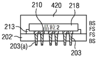
Accomplish wafer factory process (for example passivation processing) afterwards, the TSV wafer 202 of TSV 203 and a plurality of TSV crystal grain with embedding is shown in Fig. 2 A." FS " the corresponding crystal grain in the drawings or the preceding/top side of wafer, and the back/bottom side of " BS " corresponding crystal grain or wafer.As shown in Fig. 2 B, use first jointing material 206 first carrier wafer 205 to be installed to the top side of TSV wafer 202 with first unsticking temperature.Fig. 2 C is illustrated in TSV wafer attenuation (for example back of the body mill) thereby forms the attenuation TSV wafer 202 ' diagram afterwards that comprises TSV 203, and TSV 203 has most advanced and sophisticated 203 (a) of TSV of exposure.
Fig. 2 D is illustrated in and uses second jointing material 207 second carrier wafer 215 to be installed to the bottom side profile afterwards of the TSV wafer 202 ' of attenuation.Like top description, second jointing material 207 has the second unsticking temperature higher than the first unsticking temperature.Fig. 2 E is illustrated in and allows the profile of first carrier wafer 205 after the heating that attenuation TSV wafer 202 ' removes.Second carrier wafer 215 is kept being attached to the TSV wafer 202 ' of attenuation by second adhesive 207.
Like top description, the 2nd IC crystal grain can comprise the IC crystal grain of one or more how single change.In this embodiment, the TSV wafer that piles up that comprises the electronic products of formation comprises crystal grain-TSV wafer stacking.Fig. 2 F is illustrated in showing that the 2nd IC crystal grain of singleization of making crystal grain 2218 is attached to the front side of a plurality of TSV crystal grain that on the top side of attenuation TSV wafer 202 ', form, thereby forms the profile after crystal grain-wafer stacking.Crystal grain 2218 is shown having and is used for a plurality of combination conductors (convexity) 210 that FC engages.Crystal grain 2 can be semiconducter IC, MEMS device or the IC that comprises MEMS, or passive device.
Like top description, the 2nd IC crystal grain also can comprise wafer, and this wafer comprises a plurality of the 2nd IC crystal grain.In this embodiment, the TSV wafer that piles up that comprises the electronic products of formation comprises wafer-TSV wafer stacking.Fig. 2 G is illustrated in comprising the front side that the wafer 261 that shows a plurality of the 2nd IC crystal grain of making crystal grain 2218 is attached to a plurality of TSV crystal grain that on the top side of attenuation TSV wafer 202 ', form, thereby forms the profile after wafer-TSV wafer stacking.Crystal grain 2218 is shown as to have and is used for a plurality of combination conductors (convexity) 210 that FC engages.As mentioned above, crystal grain 2218 can be semiconducter IC, MEMS device or the IC that comprises MEMS, or passive device.Illustrate between the FS of crystal grain 2218 and the attenuation TSV wafer 202 ' of curable dielectric film (CDF) 213 in Fig. 2 F, and illustrate between the FS of wafer in Fig. 2 G 261 and attenuation TSV wafer 202 '.CDF 213 allows pressing; Thereby use extruding force (pressure) to come to form simultaneously junction point and formation underfill; This pressure is enough to cause being used for the convexity 210 that FC engages on the crystal grain 2218 and penetrates into CDF layer 213; Thereby between the combination characteristic on the FS of TSV crystal grain on convexity 210 and the attenuation TSV wafer 202 ' top side, form the metal bond point, heat wherein is enough to cause CDF 213 to form bottom packed layers (for example crosslinked).
Typical hot pressing condition can comprise 150-180 ℃ temperature, 35-133Kgf/cm during pressing
2Power/area during the extruding (pressure), and the extrusion time between 100-180 second (sec).Therefore, in this embodiment, conventional bottom fill process, for example fill the capillary bottom or non-conductive glue (NCP) technology is optional.
Fig. 3 A-H illustrates with example according to disclosed embodiment does not have the related ribbon diagram of mould assembling flow path; This example does not have the crystal grain that the mould assembling flow path is used for forming from crystal grain-wafer stacking singleization and piles up, and the crystal grain of singleization is piled up be attached to package substrate then.Package substrate can comprise for example organic or ceramic printed-circuit board (PCB).Fig. 3 A illustrates profile, and this profile illustrates second carrier wafer 215 and removes from the crystal grain-wafer stacking shown in Fig. 2 F.Fig. 3 B illustrates profile, and crystal grain-wafer stacking that this profile illustrates carrier and do not have wafer is installed on the section film 315.
Fig. 3 C-E illustrates no die capillaries bottom and fills flow process assembling option.Fig. 3 C is illustrated in the crystal grain-wafer stacking shown in Fig. 3 B is carried out the wafer sawing, thereby the result after a plurality of singleization stacked dies is provided.Fig. 3 D illustrates to use and comprises the technology that TC combines or quality refluxes, and the stacked die of singleization is installed on the package substrate 301 that comprises pad 302.Fig. 3 E is illustrated in the structure that capillary bottom causes after filling, thereby arranges in the slit region that between the surface of the bottom of the stacked die of singleization and substrate 301 bottom fills 313.
Fig. 3 F-H illustrates the bottom filling assembling option that no mould applies in advance.Fig. 3 F is illustrated in and places CDF film 321 between crystal grain-wafer stacking shown in Fig. 2 F and the section film 315.Fig. 3 G is illustrated in the singleization stacked die that provides after the crystal grain-wafer stacking shown in sawing Fig. 3 F.The structure that Fig. 3 H causes after illustrating and being placed on singleization stacked die on the package substrate; And cause singleization stacked die to be attached to the pressing of pad on the package substrate, and the formation that is derived from the underfill of CDF 321 between singleization stacked die and the package substrate is shown also.
Fig. 4 A-I illustrates with example according to disclosed embodiment and contains the related ribbon diagram of mould assembling flow path; This example contains the crystal grain that the mould assembling flow path is used for forming from crystal grain-wafer stacking singleization piles up, and the crystal grain of singleization is piled up be attached to package substrate then.Fig. 4 A is illustrated in mold materials 410 and is applied to the diagram afterwards of the crystal grain-wafer stacking shown in Fig. 2 F.Fig. 4 B illustrates profile, and this profile illustrates second carrier wafer 215 and removes from crystal grain-wafer stacking.Fig. 4 C illustrates most advanced and sophisticated 203 (a) side of the crystal grain of moulding-wafer stacking TSV upwards is installed on the section film 315.
Fig. 4 D-E illustrates the assembling option that flow process is filled in the capillary bottom that comprises mould.Fig. 4 D is illustrated in the moulding crystal grain shown in Fig. 4 C-wafer stacking wafer sawing, comprises a plurality of moulds result afterwards who cuts stacked die thereby provide.Fig. 4 E illustrates to use and comprises the technology that TC combines or quality refluxes, and will comprise the mould that cuts stacked die and be installed on the package substrate 301 that comprises pad 302.Fig. 4 F is illustrated in the structure that capillary bottom causes after filling, and fills 313 thereby openly cut between the surface of bottom and substrate 301 of stacked die the bottom in the slit region.
Fig. 4 G-I illustrates the bottom filling assembling option that no mould applies in advance.Fig. 4 G illustrates CDF film 321 is placed on the most advanced and sophisticated side of TSV of moulding crystal grain-wafer stacking, and the structure after upwards being installed in the most advanced and sophisticated side of moulding wafer stacking TSV on the section film 315.Fig. 4 H is illustrated in singleization of the moulding stacked die that provides after the moulding crystal grain-wafer stacking on the section film 315 shown in sawing Fig. 4 G.The singleization stacked die that Fig. 4 I illustrates moulding is placed on the structure that causes afterwards on the package substrate; And cause singleization stacked die to be attached to the pressing of pad 302 on the package substrate 301, and the formation that is derived from the underfill of CDF 321 between singleization stacked die and the package substrate 301 of moulding is shown also.
Like top description, although most advanced and sophisticated 203 (a) of outstanding TSV illustrate in the above, in other embodiments of the invention, TSV 209 can the electric access from the bottom side of TSV wafer, but outstanding from the bottom side of wafer, for example when comprising RDL.
Example
Embodiments of the invention are further specified by the example of following mask body, and these object lessons should not be construed as scope or the content that limits the embodiment of the invention by any way.
Fig. 5 be can be generally as the viscosity temperature of three kinds of different example jointing materials of combination adhesive described here (℃) figure.Adhesive A can be used for low unsticking temperature adhesive, and adhesive B or C are used for higher unsticking temperature adhesive.Temperature as the softening temperature in this use refers to: in the viscosity of this temperature is the minimal viscosity that the opposing unsticking needs, for example 200PaS at least.Curve A is by MO, the Brewer Science WaferBOND of the Brewer Science manufactured of Springfield (Springeld)
TMThe viscograph of HT-10.10 coating.Curve B and C provide viscograph for other material, and these other materials provide the unsticking temperature higher than the unsticking temperature shown in the curve A.
The higher unsticking temperature of a kind of example adhesive source is from Sumitomo 3M, and this adhesive is the UV cure adhesive.UV solidified liquid adhesive can be similar to the such use of HT10.10, and it is additional to be used for carrier wafer.Because like this, thereby to the border of glass, forming vesicle through laser explosure, succeeded by removing from wafer through removing band, the UV cure adhesive possibly remove from glass or other carrier.Sumitomo 3M is by Sumitomo 3M Ltd. manufactured, have the solar heat protection ability of anti-about 250 ℃ unsticking, as in Fig. 5 for shown in curve B and the C.
In example sequence, second adhesive of higher unsticking temperature is added to the TSV wafer, and the TSV wafer has the low temperature adhesive that combines on the another side, be similar to shown in Fig. 2 D.Second adhesive UV then solidifies.First adhesive being selected property then removes, and for example is that the first adhesive HT10.10 removes about 200 ℃, stays second carrier wafer by second adhesive attachment simultaneously.After thereby die attach forms crystal grain-wafer stacking to the TSV wafer; Laser explosure can be used to form bubble; Thereby before singleization of crystal grain-wafer stacking, remove the material of glass carrier and UV curing, to form the stacked die of singleization from crystal grain-wafer stacking.
Embodiments of the invention can be incorporated in the various technological processes, thereby form various devices and Related product.Semiconductor substrate can be therein and/or the layer on it comprise various elements.These can comprise barrier layer, other dielectric layer, device architecture, the active element that comprises source region, drain region, bit line, base stage, emitter, collector electrode, lead, conductive through hole and passive component etc.In addition, embodiments of the invention can be used to comprise the various technologies of bipolar, CMOS, BiCMOS and MEMS.
Therefore intention covers and has the characteristic under the example embodiment background, described or or the embodiment of more various combination of step, and example embodiment has the whole of such characteristic or step or more only.Those skilled in the art recognize that many other embodiment also are possible with changing in the scope of the invention that requires to protect.
Claims (13)
1. method that electronic products is piled up in formation comprises:
Use has first jointing material of the first unsticking temperature, and first carrier wafer is installed to the top side of running through substrate through vias (TSV) wafer, and said TSV wafer comprises TSV crystal grain;
Make the bottom side attenuation of said TSV wafer from said TSV wafer, thereby form attenuation TSV wafer, wherein said attenuation is included in and exposes the TSV tip that embeds on the said TSV wafer, thereby it is most advanced and sophisticated to form the TSV that exposes;
Use second jointing material that second carrier wafer is installed to said bottom side, wherein said second jointing material has the second unsticking temperature that is higher than the said first unsticking temperature;
Said attenuation TSV wafer is heated to above the temperature of the said first unsticking temperature, thereby removes said first carrier wafer from said attenuation TSV wafer; And
At least one the 2nd IC crystal grain is attached to the said TSV crystal grain on the said top side of said attenuation TSV wafer, thus form comprise electronic products pile up the TSV wafer.
2. method according to claim 1, wherein said first jointing material and said second jointing material all comprise thermoplastics.
3. method according to claim 1, the TSV tip of wherein said exposure are most advanced and sophisticated from the outstanding TSV of the outstanding at least 5 μ m in bottom side of said attenuation TSV wafer.
4. method according to claim 1, further being included in and between the said top side of said the 2nd IC crystal grain and said TSV wafer curable dielectric film being provided is CDF; And said the 2nd IC crystal grain of wherein said combination comprises heat pressing process; Thereby said heat pressing process provides compression molding to form the bottom from said CDF in single processing step and fills, thereby and provide joint with combine said the 2nd IC crystal grain form said comprise electronic products pile up the TSV wafer.
5. method according to claim 1, the said TSV wafer that piles up that comprises electronic products of wherein said formation further is included in after the said combination of said the 2nd IC crystal grain, carries out the bottom with underfill or non-conductive glue and fills.
6. method according to claim 4, said the 2nd IC crystal grain of wherein said combination comprises flip bonded.
7. method according to claim 4, wherein said the 2nd IC crystal grain comprises a plurality of TSV, and said the 2nd IC crystal grain of wherein said combination comprise said the 2nd IC crystal grain towards last combination.
8. method according to claim 1 further comprises:
Remove said second carrier wafer from the said TSV wafer that piles up that comprises electronic products; And
With said comprise electronic products pile up the sawing of TSV wafer, thereby form a plurality of singleization pile up IC crystal grain.
9. method according to claim 8 further comprises:
With said a plurality of singleization pile up IC crystal grain at least one be attached to the package substrate that has planar pad above that, and
Carrying out the capillary bottom with underfill or non-conductive glue fills.
10. method according to claim 8, the TSV tip of wherein said exposure are most advanced and sophisticated from the outstanding TSV of the outstanding at least 5 μ m in said bottom side of said attenuation TSV wafer, and said method further comprises:
Before said sawing, on said outstanding TSV tip, curable dielectric film being provided is CDF,
Have above that place said a plurality of singleization on the package substrate of planar pad pile up at least one of IC crystal grain, and
Comprise the combination of heat pressing process; Thereby said heat pressing process provides compression molding to form the bottom from said CDF in single processing step and fills, thereby and provides joint the said outstanding TSV tip of piling up IC crystal grain of said singleization to be attached to the said planar pad of said package substrate.
11. method according to claim 1 further comprises:
Form the mould layer, be included in said the 2nd IC crystal grain of said combination afterwards with mold materials secondary moulding, thereby cover said the 2nd IC crystal grain;
Remove said second carrier wafer from the said TSV wafer that piles up that comprises electronic products, and
With said comprise electronic products pile up the sawing of TSV wafer, thereby form a plurality of singleization pile up IC crystal grain.
12. method according to claim 11; Further comprise with said a plurality of singleization pile up IC crystal grain at least one be attached to the package substrate that has planar pad above that, and carry out the capillary bottom with underfill or non-conductive glue then and fill.
13. method according to claim 11, the TSV tip of wherein said exposure are most advanced and sophisticated from the outstanding TSV of the outstanding at least 5 μ m in said bottom side of said attenuation TSV wafer, said method further comprises:
Before said wafer sawing, on said outstanding TSV tip, curable dielectric film being provided is CDF,
Have above that place said a plurality of singleization on the package substrate of planar pad pile up at least one of IC crystal grain, and
Comprise second of heat pressing process and combine, fill, thereby and provide joint said outstanding TSV tip to be attached to the said planar pad of package substrate thereby said heat pressing process provides compression molding to form the bottom from said CDF in single processing step.
Applications Claiming Priority (3)
| Application Number | Priority Date | Filing Date | Title |
|---|---|---|---|
| US12/694,012 US8017439B2 (en) | 2010-01-26 | 2010-01-26 | Dual carrier for joining IC die or wafers to TSV wafers |
| US12/694,012 | 2010-01-26 | ||
| PCT/US2010/060927 WO2011093955A2 (en) | 2010-01-26 | 2010-12-17 | Dual carrier for joining ic die or wafers to tsv wafers |
Publications (1)
| Publication Number | Publication Date |
|---|---|
| CN102844859A true CN102844859A (en) | 2012-12-26 |
Family
ID=44309261
Family Applications (1)
| Application Number | Title | Priority Date | Filing Date |
|---|---|---|---|
| CN2010800658302A Pending CN102844859A (en) | 2010-01-26 | 2010-12-17 | Dual carrier for joining ic die or wafers to tsv wafers |
Country Status (4)
| Country | Link |
|---|---|
| US (1) | US8017439B2 (en) |
| JP (1) | JP2013518432A (en) |
| CN (1) | CN102844859A (en) |
| WO (1) | WO2011093955A2 (en) |
Cited By (4)
| Publication number | Priority date | Publication date | Assignee | Title |
|---|---|---|---|---|
| CN105189337A (en) * | 2013-05-10 | 2015-12-23 | 株式会社村田制作所 | A microelectromechanical device and a method of manufacturing |
| CN107644843A (en) * | 2016-07-22 | 2018-01-30 | 中芯国际集成电路制造(天津)有限公司 | Method for manufacturing wafer stack |
| CN108878465A (en) * | 2018-06-07 | 2018-11-23 | 复旦大学 | Cmos image sensor and preparation method thereof based on back electrode connection |
| CN114724967A (en) * | 2022-06-08 | 2022-07-08 | 江苏芯德半导体科技有限公司 | Packaging method of heterogeneous chip packaging structure with TSV |
Families Citing this family (37)
| Publication number | Priority date | Publication date | Assignee | Title |
|---|---|---|---|---|
| US8232140B2 (en) | 2009-03-27 | 2012-07-31 | Taiwan Semiconductor Manufacturing Company, Ltd. | Method for ultra thin wafer handling and processing |
| US9224630B2 (en) * | 2010-03-31 | 2015-12-29 | Ev Group E. Thallner Gmbh | Method for producing a wafer provided with chips |
| US8866301B2 (en) * | 2010-05-18 | 2014-10-21 | Taiwan Semiconductor Manufacturing Company, Ltd. | Package systems having interposers with interconnection structures |
| US8928159B2 (en) | 2010-09-02 | 2015-01-06 | Taiwan Semiconductor Manufacturing & Company, Ltd. | Alignment marks in substrate having through-substrate via (TSV) |
| US8786066B2 (en) * | 2010-09-24 | 2014-07-22 | Intel Corporation | Die-stacking using through-silicon vias on bumpless build-up layer substrates including embedded-dice, and processes of forming same |
| TW201241941A (en) * | 2010-10-21 | 2012-10-16 | Sumitomo Bakelite Co | A method for manufacturing an electronic equipment, and the electronic equipment obtained by using the method, as well as a method for manufacturing electronics and electronic parts, and the electronics and the electronic parts obtained using the method |
| US9324905B2 (en) | 2011-03-15 | 2016-04-26 | Micron Technology, Inc. | Solid state optoelectronic device with preformed metal support substrate |
| KR20120123919A (en) * | 2011-05-02 | 2012-11-12 | 삼성전자주식회사 | Method for manufacturing a chip stacked semiconductor package and the chip stacked semiconductor package thereof |
| US8569086B2 (en) * | 2011-08-24 | 2013-10-29 | Taiwan Semiconductor Manufacturing Company, Ltd. | Semiconductor device and method of dicing semiconductor devices |
| US9343430B2 (en) * | 2011-09-02 | 2016-05-17 | Maxim Integrated Products, Inc. | Stacked wafer-level package device |
| US8383460B1 (en) * | 2011-09-23 | 2013-02-26 | GlobalFoundries, Inc. | Method for fabricating through substrate vias in semiconductor substrate |
| CN103066049B (en) * | 2011-10-24 | 2015-09-02 | 联致科技股份有限公司 | Base plate for packaging and method for making thereof |
| EP2648214B1 (en) | 2012-04-05 | 2019-06-12 | ams AG | Methods of producing a semiconductor device with a through-substrate via |
| US9583365B2 (en) | 2012-05-25 | 2017-02-28 | Taiwan Semiconductor Manufacturing Company, Ltd. | Method of forming interconnects for three dimensional integrated circuit |
| TWI464811B (en) * | 2012-06-05 | 2014-12-11 | Yi Ham Chiang | A semiconductor packaging method and structure |
| EP2873095B1 (en) * | 2012-07-11 | 2017-06-14 | Hewlett-Packard Development Company, L.P. | Semiconductor secured to substrate via hole in substrate |
| US8816507B2 (en) * | 2012-07-26 | 2014-08-26 | Taiwan Semiconductor Manufacturing Company, Ltd. | Package-on-Package structures having buffer dams and method for forming the same |
| CN104684840A (en) | 2012-07-31 | 2015-06-03 | 惠普发展公司,有限责任合伙企业 | Device including interposer between semiconductor and substrate |
| TWI467723B (en) * | 2012-09-26 | 2015-01-01 | 矽品精密工業股份有限公司 | Semiconductor package and method of forming the same |
| KR102077248B1 (en) | 2013-01-25 | 2020-02-13 | 삼성전자주식회사 | Methods for processing substrates |
| CN103996351B (en) * | 2013-02-20 | 2020-01-21 | 泰科消防及安全有限公司 | Adhesive bonded article protection label |
| KR102038488B1 (en) | 2013-02-26 | 2019-10-30 | 삼성전자 주식회사 | Method for fabricating semiconductor package |
| KR102084540B1 (en) | 2013-10-16 | 2020-03-04 | 삼성전자주식회사 | Semiconductor package an And Method Of Fabricating The Same |
| KR20150120570A (en) * | 2014-04-17 | 2015-10-28 | 에스케이하이닉스 주식회사 | Semiconductor package and the method for manufacturing of the same |
| KR20150123420A (en) * | 2014-04-24 | 2015-11-04 | 에스케이하이닉스 주식회사 | Semiconductor package and the method for manufacturing of the same |
| KR102254104B1 (en) | 2014-09-29 | 2021-05-20 | 삼성전자주식회사 | Semiconductor package |
| US9888579B2 (en) * | 2015-03-05 | 2018-02-06 | Invensas Corporation | Pressing of wire bond wire tips to provide bent-over tips |
| US9886193B2 (en) | 2015-05-15 | 2018-02-06 | International Business Machines Corporation | Architecture and implementation of cortical system, and fabricating an architecture using 3D wafer scale integration |
| JP6572043B2 (en) * | 2015-07-24 | 2019-09-04 | 積水化学工業株式会社 | Semiconductor wafer protection film |
| JP7201386B2 (en) | 2018-10-23 | 2023-01-10 | 株式会社ダイセル | Semiconductor device manufacturing method |
| KR102609475B1 (en) * | 2018-10-23 | 2023-12-06 | 주식회사 다이셀 | Semiconductor device manufacturing method |
| JP7224138B2 (en) * | 2018-10-23 | 2023-02-17 | 株式会社ダイセル | Semiconductor device manufacturing method |
| KR20200113069A (en) | 2019-03-20 | 2020-10-06 | 삼성전자주식회사 | Method of manufacturing semiconductor device |
| EP4034867A4 (en) * | 2019-09-26 | 2023-09-27 | Illumina, Inc. | Fabricating wafers with electrical contacts on a surface parallel to an active surface |
| CN111128914A (en) * | 2019-12-25 | 2020-05-08 | 上海先方半导体有限公司 | Low-warpage multi-chip packaging structure and manufacturing method thereof |
| US11728248B2 (en) | 2021-07-01 | 2023-08-15 | Deca Technologies Usa, Inc. | Fully molded semiconductor structure with through silicon via (TSV) vertical interconnects |
| US11616003B2 (en) * | 2021-07-01 | 2023-03-28 | Deca Technologies Usa, Inc. | Stackable fully molded semiconductor structure with through silicon via (TSV) vertical interconnects |
Citations (4)
| Publication number | Priority date | Publication date | Assignee | Title |
|---|---|---|---|---|
| US20060076661A1 (en) * | 2003-12-17 | 2006-04-13 | Sergey Savastiouk | Attachment of integrated circuit structures and other substrates to substrates with vias |
| US20070007641A1 (en) * | 2005-07-08 | 2007-01-11 | Kang-Wook Lee | Chip-embedded interposer structure and fabrication method thereof, wafer level stack structure and resultant package structure |
| US20080295325A1 (en) * | 2007-05-30 | 2008-12-04 | Sriram Muthukumar | Multi-chip packaging using an interposer such as a silicon based interposer with through-silicon-vias |
| US20090280602A1 (en) * | 2008-05-12 | 2009-11-12 | Texas Instruments Incorporated | Double wafer carrier process for creating integrated circuit die with through-silicon vias and micro-electro-mechanical systems protected by a hermetic cavity created at the wafer level |
Family Cites Families (9)
| Publication number | Priority date | Publication date | Assignee | Title |
|---|---|---|---|---|
| JP4551638B2 (en) * | 2003-08-01 | 2010-09-29 | 富士フイルム株式会社 | Method for manufacturing solid-state imaging device |
| JP4085972B2 (en) * | 2003-12-08 | 2008-05-14 | セイコーエプソン株式会社 | Manufacturing method of semiconductor device |
| JP2007311385A (en) * | 2006-05-16 | 2007-11-29 | Sony Corp | Process for fabricating semiconductor device, and semiconductor device |
| JP2008103395A (en) * | 2006-10-17 | 2008-05-01 | Seiko Epson Corp | Semiconductor module and manufacturing method thereof |
| TWI331391B (en) * | 2007-03-20 | 2010-10-01 | Siliconware Precision Industries Co Ltd | Stackable semiconductor device and fabrication method thereof |
| US7973416B2 (en) * | 2008-05-12 | 2011-07-05 | Texas Instruments Incorporated | Thru silicon enabled die stacking scheme |
| US8278142B2 (en) * | 2008-05-22 | 2012-10-02 | Texas Instruments Incorporated | Combined metallic bonding and molding for electronic assemblies including void-reduced underfill |
| US7915080B2 (en) * | 2008-12-19 | 2011-03-29 | Texas Instruments Incorporated | Bonding IC die to TSV wafers |
| US8263497B2 (en) * | 2009-01-13 | 2012-09-11 | International Business Machines Corporation | High-yield method of exposing and contacting through-silicon vias |
-
2010
- 2010-01-26 US US12/694,012 patent/US8017439B2/en active Active
- 2010-12-17 JP JP2012551156A patent/JP2013518432A/en active Pending
- 2010-12-17 CN CN2010800658302A patent/CN102844859A/en active Pending
- 2010-12-17 WO PCT/US2010/060927 patent/WO2011093955A2/en active Application Filing
Patent Citations (4)
| Publication number | Priority date | Publication date | Assignee | Title |
|---|---|---|---|---|
| US20060076661A1 (en) * | 2003-12-17 | 2006-04-13 | Sergey Savastiouk | Attachment of integrated circuit structures and other substrates to substrates with vias |
| US20070007641A1 (en) * | 2005-07-08 | 2007-01-11 | Kang-Wook Lee | Chip-embedded interposer structure and fabrication method thereof, wafer level stack structure and resultant package structure |
| US20080295325A1 (en) * | 2007-05-30 | 2008-12-04 | Sriram Muthukumar | Multi-chip packaging using an interposer such as a silicon based interposer with through-silicon-vias |
| US20090280602A1 (en) * | 2008-05-12 | 2009-11-12 | Texas Instruments Incorporated | Double wafer carrier process for creating integrated circuit die with through-silicon vias and micro-electro-mechanical systems protected by a hermetic cavity created at the wafer level |
Cited By (8)
| Publication number | Priority date | Publication date | Assignee | Title |
|---|---|---|---|---|
| CN105189337A (en) * | 2013-05-10 | 2015-12-23 | 株式会社村田制作所 | A microelectromechanical device and a method of manufacturing |
| CN105189337B (en) * | 2013-05-10 | 2017-05-03 | 株式会社村田制作所 | A microelectromechanical device and a method of manufacturing |
| US9663352B2 (en) | 2013-05-10 | 2017-05-30 | Murata Manufacturing Co., Ltd. | Microelectromechanical device and a method of manufacturing |
| CN107644843A (en) * | 2016-07-22 | 2018-01-30 | 中芯国际集成电路制造(天津)有限公司 | Method for manufacturing wafer stack |
| CN107644843B (en) * | 2016-07-22 | 2020-07-28 | 中芯国际集成电路制造(天津)有限公司 | Wafer stack manufacturing method |
| CN108878465A (en) * | 2018-06-07 | 2018-11-23 | 复旦大学 | Cmos image sensor and preparation method thereof based on back electrode connection |
| CN108878465B (en) * | 2018-06-07 | 2020-07-07 | 复旦大学 | CMOS image sensor based on back electrode connection and preparation method thereof |
| CN114724967A (en) * | 2022-06-08 | 2022-07-08 | 江苏芯德半导体科技有限公司 | Packaging method of heterogeneous chip packaging structure with TSV |
Also Published As
| Publication number | Publication date |
|---|---|
| WO2011093955A3 (en) | 2011-10-06 |
| US8017439B2 (en) | 2011-09-13 |
| US20110183464A1 (en) | 2011-07-28 |
| JP2013518432A (en) | 2013-05-20 |
| WO2011093955A2 (en) | 2011-08-04 |
Similar Documents
| Publication | Publication Date | Title |
|---|---|---|
| CN102844859A (en) | Dual carrier for joining ic die or wafers to tsv wafers | |
| US7915080B2 (en) | Bonding IC die to TSV wafers | |
| KR101500038B1 (en) | Sawing underfill in packaging processes | |
| US8253258B2 (en) | Semiconductor device with hollow and throughhole and method of manufacturing same | |
| CN101409266B (en) | Package structure | |
| US8293583B2 (en) | Method for manufacturing semiconductor device | |
| EP2111636B1 (en) | High thermal performance packaging for circuit dies | |
| TWI757587B (en) | Semiconductor device | |
| CN103247541B (en) | Semiconductor device and manufacture method thereof | |
| CN102479725A (en) | Stackable semiconductor assembly with bump/flange heat spreader and dual build-up circuitry | |
| CN102844861A (en) | Tce compensation for ic package substrates for reduced die warpage assembly | |
| CN103165531B (en) | Die structure and method of fabrication thereof | |
| CN103247547B (en) | For having the no-reflow underfill of the packaging part inserting framework | |
| CN102256452A (en) | Circuit board with built-in semiconductor chip and method of manufacturing the same | |
| TWI335645B (en) | Method and system for flip chip packaging | |
| US9318473B2 (en) | Semiconductor device including a polymer disposed on a carrier | |
| CN104064529A (en) | Semiconductor component, semiconductor module and methods for producing a semiconductor component and a semiconductor module | |
| JP6213554B2 (en) | Semiconductor device | |
| TW200945456A (en) | Package method for flip chip | |
| US11309219B2 (en) | Method for manufacturing semiconductor device | |
| CN113196465A (en) | Fan-out package with recess | |
| US20220384468A1 (en) | Semiconductor device and semiconductor device manufacturing method | |
| CN103295998B (en) | There is packaging part of intermediary's framework and forming method thereof | |
| JP7172022B2 (en) | Semiconductor device manufacturing method | |
| KR101745728B1 (en) | Method for three dimensional stacking of semiconductor chip |
Legal Events
| Date | Code | Title | Description |
|---|---|---|---|
| C06 | Publication | ||
| PB01 | Publication | ||
| C10 | Entry into substantive examination | ||
| SE01 | Entry into force of request for substantive examination | ||
| C05 | Deemed withdrawal (patent law before 1993) | ||
| WD01 | Invention patent application deemed withdrawn after publication |
Application publication date: 20121226 |