CN1155993C - 用横向生长制备氮化镓层 - Google Patents
用横向生长制备氮化镓层 Download PDFInfo
- Publication number
- CN1155993C CN1155993C CNB99813628XA CN99813628A CN1155993C CN 1155993 C CN1155993 C CN 1155993C CN B99813628X A CNB99813628X A CN B99813628XA CN 99813628 A CN99813628 A CN 99813628A CN 1155993 C CN1155993 C CN 1155993C
- Authority
- CN
- China
- Prior art keywords
- gallium nitride
- layer
- growth
- horizontal
- sidewall
- Prior art date
- Legal status (The legal status is an assumption and is not a legal conclusion. Google has not performed a legal analysis and makes no representation as to the accuracy of the status listed.)
- Expired - Fee Related
Links
Images


Classifications
-
- H—ELECTRICITY
- H01—ELECTRIC ELEMENTS
- H01L—SEMICONDUCTOR DEVICES NOT COVERED BY CLASS H10
- H01L21/00—Processes or apparatus adapted for the manufacture or treatment of semiconductor or solid state devices or of parts thereof
- H01L21/02—Manufacture or treatment of semiconductor devices or of parts thereof
- H01L21/04—Manufacture or treatment of semiconductor devices or of parts thereof the devices having at least one potential-jump barrier or surface barrier, e.g. PN junction, depletion layer or carrier concentration layer
- H01L21/18—Manufacture or treatment of semiconductor devices or of parts thereof the devices having at least one potential-jump barrier or surface barrier, e.g. PN junction, depletion layer or carrier concentration layer the devices having semiconductor bodies comprising elements of Group IV of the Periodic System or AIIIBV compounds with or without impurities, e.g. doping materials
- H01L21/20—Deposition of semiconductor materials on a substrate, e.g. epitaxial growth solid phase epitaxy
-
- C—CHEMISTRY; METALLURGY
- C30—CRYSTAL GROWTH
- C30B—SINGLE-CRYSTAL GROWTH; UNIDIRECTIONAL SOLIDIFICATION OF EUTECTIC MATERIAL OR UNIDIRECTIONAL DEMIXING OF EUTECTOID MATERIAL; REFINING BY ZONE-MELTING OF MATERIAL; PRODUCTION OF A HOMOGENEOUS POLYCRYSTALLINE MATERIAL WITH DEFINED STRUCTURE; SINGLE CRYSTALS OR HOMOGENEOUS POLYCRYSTALLINE MATERIAL WITH DEFINED STRUCTURE; AFTER-TREATMENT OF SINGLE CRYSTALS OR A HOMOGENEOUS POLYCRYSTALLINE MATERIAL WITH DEFINED STRUCTURE; APPARATUS THEREFOR
- C30B25/00—Single-crystal growth by chemical reaction of reactive gases, e.g. chemical vapour-deposition growth
- C30B25/02—Epitaxial-layer growth
-
- C—CHEMISTRY; METALLURGY
- C30—CRYSTAL GROWTH
- C30B—SINGLE-CRYSTAL GROWTH; UNIDIRECTIONAL SOLIDIFICATION OF EUTECTIC MATERIAL OR UNIDIRECTIONAL DEMIXING OF EUTECTOID MATERIAL; REFINING BY ZONE-MELTING OF MATERIAL; PRODUCTION OF A HOMOGENEOUS POLYCRYSTALLINE MATERIAL WITH DEFINED STRUCTURE; SINGLE CRYSTALS OR HOMOGENEOUS POLYCRYSTALLINE MATERIAL WITH DEFINED STRUCTURE; AFTER-TREATMENT OF SINGLE CRYSTALS OR A HOMOGENEOUS POLYCRYSTALLINE MATERIAL WITH DEFINED STRUCTURE; APPARATUS THEREFOR
- C30B29/00—Single crystals or homogeneous polycrystalline material with defined structure characterised by the material or by their shape
- C30B29/10—Inorganic compounds or compositions
- C30B29/40—AIIIBV compounds wherein A is B, Al, Ga, In or Tl and B is N, P, As, Sb or Bi
- C30B29/403—AIII-nitrides
- C30B29/406—Gallium nitride
-
- H—ELECTRICITY
- H01—ELECTRIC ELEMENTS
- H01L—SEMICONDUCTOR DEVICES NOT COVERED BY CLASS H10
- H01L21/00—Processes or apparatus adapted for the manufacture or treatment of semiconductor or solid state devices or of parts thereof
- H01L21/02—Manufacture or treatment of semiconductor devices or of parts thereof
- H01L21/02104—Forming layers
- H01L21/02365—Forming inorganic semiconducting materials on a substrate
- H01L21/02367—Substrates
- H01L21/0237—Materials
- H01L21/02373—Group 14 semiconducting materials
- H01L21/02378—Silicon carbide
-
- H—ELECTRICITY
- H01—ELECTRIC ELEMENTS
- H01L—SEMICONDUCTOR DEVICES NOT COVERED BY CLASS H10
- H01L21/00—Processes or apparatus adapted for the manufacture or treatment of semiconductor or solid state devices or of parts thereof
- H01L21/02—Manufacture or treatment of semiconductor devices or of parts thereof
- H01L21/02104—Forming layers
- H01L21/02365—Forming inorganic semiconducting materials on a substrate
- H01L21/02436—Intermediate layers between substrates and deposited layers
- H01L21/02439—Materials
- H01L21/02455—Group 13/15 materials
- H01L21/02458—Nitrides
-
- H—ELECTRICITY
- H01—ELECTRIC ELEMENTS
- H01L—SEMICONDUCTOR DEVICES NOT COVERED BY CLASS H10
- H01L21/00—Processes or apparatus adapted for the manufacture or treatment of semiconductor or solid state devices or of parts thereof
- H01L21/02—Manufacture or treatment of semiconductor devices or of parts thereof
- H01L21/02104—Forming layers
- H01L21/02365—Forming inorganic semiconducting materials on a substrate
- H01L21/02518—Deposited layers
- H01L21/02521—Materials
- H01L21/02538—Group 13/15 materials
- H01L21/0254—Nitrides
-
- H—ELECTRICITY
- H01—ELECTRIC ELEMENTS
- H01L—SEMICONDUCTOR DEVICES NOT COVERED BY CLASS H10
- H01L21/00—Processes or apparatus adapted for the manufacture or treatment of semiconductor or solid state devices or of parts thereof
- H01L21/02—Manufacture or treatment of semiconductor devices or of parts thereof
- H01L21/02104—Forming layers
- H01L21/02365—Forming inorganic semiconducting materials on a substrate
- H01L21/02612—Formation types
- H01L21/02617—Deposition types
- H01L21/02636—Selective deposition, e.g. simultaneous growth of mono- and non-monocrystalline semiconductor materials
- H01L21/02639—Preparation of substrate for selective deposition
-
- H—ELECTRICITY
- H01—ELECTRIC ELEMENTS
- H01L—SEMICONDUCTOR DEVICES NOT COVERED BY CLASS H10
- H01L21/00—Processes or apparatus adapted for the manufacture or treatment of semiconductor or solid state devices or of parts thereof
- H01L21/02—Manufacture or treatment of semiconductor devices or of parts thereof
- H01L21/02104—Forming layers
- H01L21/02365—Forming inorganic semiconducting materials on a substrate
- H01L21/02612—Formation types
- H01L21/02617—Deposition types
- H01L21/02636—Selective deposition, e.g. simultaneous growth of mono- and non-monocrystalline semiconductor materials
- H01L21/02647—Lateral overgrowth
- H01L21/0265—Pendeoepitaxy
Abstract
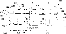
一种用掩模(109)图形化的碳化硅衬底(102)上的氮化镓基层(104),它包括其中的窗口阵列,并被腐蚀穿过窗口阵列,以便在氮化镓基层中确定柱(106)及其间的沟槽(107)。每一个柱包含侧壁(105)和其上带有掩模的顶部。柱的侧壁被横向生长进入沟槽,从而形成氮化镓半导体层(108a)。在这一横向生长期间,掩模阻挡从柱顶的成核和垂直生长。因此,横向地生长进入沟槽,悬挂在柱的侧壁。柱的侧壁可横向生长进入沟槽,直至横向生长的侧壁在沟槽中接合,从而形成氮化镓半导体层。柱的侧壁横向生长可继续进行,致使氮化镓层垂直地生长穿过掩模中的窗口,并横向过生长到柱顶的掩模上,从而形成氮化镓半导体层(108b)。横向过生长能继续进行,直到生长的侧壁在掩模上接合,从而形成连续的氮化镓半导体层。在连续的氮化镓半导体层中可以制作微电子器件(110)。
Description
技术领域
本发明涉及微电子器件及制造方法,更确切地说是涉及到氮化镓半导体器件及其制造方法。
背景技术
用于包括但不限于晶体管、场发射器以及光电子器件的微电子器件的氮化镓,正受到广泛研究。可以理解,如此处所用的那样,氮化镓也包括诸如铝镓氮、铟镓氮以及铝铟镓氮之类的氮化镓合金。
制造氮化镓基微电子器件的主要问题是制备低缺陷密度的氮化镓半导体层。众所周知,缺陷密度的一个来源是其上生长氮化镓层的衬底。因此,尽管氮化镓层已被生长在蓝宝石衬底上,但已知,为减少缺陷密度而把氮化镓层生长在本身制作在碳化硅衬底上的氮化铝缓冲层上。尽管有这些进展,仍然希望继续降低缺陷密度。
还已知通过掩模中的窗口来制造氮化镓结构。例如,在制造场发射器阵列的过程中,已知在条形或圆形图形化衬底上选择性地生长氮化镓。见例如Nam等人的论文:″Selective Growth of GaN and Al0.2Ga0.8Non GaN/AlN/6H-SiC(0001)Multilayer Substrates Via OrganometallicVapor Phase Epitaxy″,Proceedings of the Materials Research Society,December 1996,和″Growth of GaN and Al0.2Ga0.8N on PatterenedSubstrates via Organometallic Vapor Phase Epitaxy″,Japanese Journalof Applied Physics,Vol.36,Part 2,No.5A,May 1997,pp.L532-L535.正如这些论文所披露的,在一定条件下,可能发生不希望的脊形生长或横向过度生长。
公布了的PCT申请WO 98/47170描述了一种生长氮化物半导体晶体的方法,该晶体的缺陷非常少并能够用作衬底,此方法包含下列步骤:制作配备有多个第一窗口的第一选择性生长掩模,用来选择性地暴露具有主平面且包括由不同于氮化物半导体的材料制成的不同类型的衬底的支座上的支持物表面;利用气态III族元素源和气态氮源,生长氮化物半导体,直到各个相邻窗口中从暴露于窗口的支持物表面生长的氮化物半导体晶体部分在选择性生长掩模的上表面上彼此接合。
发明内容
因此,本发明的一个目的在于提供制备氮化镓半导体层的改进方法,以及如此制造的改进的氮化镓层。
本发明的另一目的在于提供制造能具有低缺陷密度的氮化镓半导体层的方法,以及如此制造的氮化镓半导体层。
根据本发明,借助于用其中包含窗口阵列的掩模来掩蔽碳化硅衬底上的氮化镓基层,并通过窗口阵列来腐蚀氮化镓基层,从而确定氮化镓基层中的多个柱及其间的多个沟槽,而提供了这些和其它的目的。每一个柱包含侧壁和其上带有掩模的顶部。柱的侧壁被横向生长进入沟槽,从而形成氮化镓半导体层。在此横向生长期间,掩模阻止来自柱顶的成核和垂直生长。因此,横向生长进入沟槽,从柱侧壁悬挂下来。这种生长形式按拉丁文“悬挂”之意,在此被称为悬挂外延(pendeoepitaxy)。在氮化镓半导体层中可以制作微电子器件。
根据本发明的另一方面,柱侧壁被横向生长进入沟槽,直到横向生长的侧壁在沟槽中接合,从而形成氮化镓半导体层。从柱侧壁的横向生长可继续进行,使氮化镓垂直生长通过掩模中的窗口,进而横向生长到柱顶掩模上,从而形成氮化镓半导体层。该横向生长能够继续,直到生长的侧壁在掩模上接合,从而形成连续的氮化镓半导体层。在此连续的氮化镓半导体层中可以制作微电子器件。
已经发现,根据本发明,位错缺陷并不从柱的侧壁有明显的传播,所以横向生长的柱侧壁是相对无缺陷的。而且,在生长期间,已发现在柱顶明显的垂直生长被掩模所阻止,故相对无缺陷横向生长自侧壁发生至掩模上。柱顶的明显成核亦被优先阻止。因此,生长的氮化镓半导体层是相对无缺陷的。
从而,作为柱上的帽层的掩模的作用在于,强制有选择的氮化镓同质外延生长只发生在侧壁上。与氮化镓籽晶层的异质外延生长相关的缺陷被钉匝在掩模之下。通过侧壁生长和横向生长的组合,经一步再生长,就可在晶片的整个表面上制备出相对无缺陷氮化镓的完整接合层。
可用金属有机汽相外延(MOVPE)来横向生长悬挂外延的氮化镓半导体层。例如,可用三乙基镓(TEG)和氨(NH3)产物母体,在大约1000-1100℃和大约45Torr(大约6×10⁴Pa)下横向生长横向氮化镓层。优选条件为TEG约13-39μmol/min和NH3约1500sccm与大约3000sccm H2稀释剂组合使用。最优选的条件是:在温度约为1100℃和45Torr(大约6×10⁴Pa)下,TEG 约为26μmol/min,NH3约为1500sccm,而H2约为3000sccm。氮化镓基层最好被制作在其本身包含诸如其上的氮化铝之类的缓冲层的6H-SiC(0001)之类的衬底上。可以使用氮化镓之类的其它缓冲层。也可以使用多层衬底和缓冲层。
包含侧壁的氮化镓基层可以通过在氮化镓基层中形成沟槽来制备,使沟槽确定侧壁。或者,侧壁可以通过在氮化镓基层上形成被掩蔽的柱来制作,被掩蔽的柱含有侧壁并确定沟槽。一系列交替的沟槽和被掩蔽的柱最好被制作成形成多个侧壁。柱被制作成使顶部表面而非侧壁受到掩蔽。如上述,沟槽和/或柱可以通过掩蔽和选择腐蚀来形成。或者可以使用选择外延生长、腐蚀与生长的组合、或者其它技术。可以在柱成型之后在柱顶形成掩模。沟槽可延伸进入到缓冲层和/或衬底中,使槽底处于缓冲层内,最好在碳化硅衬底内。
氮化镓基层中的柱侧壁被横向生长进入沟槽,从而形成其缺陷密度较氮化镓基层缺陷密度低的横向氮化镓层。虽然自柱顶的垂直生长被其上的掩模减弱和抑制,沟槽中还是可能发生某些垂直生长。横向生长的氮化镓层在垂直方向生长穿过掩模中的窗口,同时传播较低的缺陷密度。随着该垂直生长高度延伸穿过掩模窗口,在掩模之上发生横向生长,同时传播较低的缺陷密度,从而在掩模之上形成生长横向氮化镓层。
根据本发明,氮化镓半导体结构包括碳化硅衬底和此碳化硅衬底上多个氮化镓柱。每一个柱包含一个侧壁、一个顶部,并确定其间的多个沟槽。柱顶部上提供一个帽层。横向氮化镓层自柱侧壁横向延伸进入沟槽。横向氮化镓层也可称为悬挂外延的氮化镓层。横向氮化镓层可以是在两个相邻侧壁之间延伸横跨其间沟槽的连续横向氮化镓层。
横向氮化镓层也可垂直地延伸通过窗口阵列。生长的横向氮化镓层也可以被制作成在帽层上横向延伸。该生长的横向氮化镓层可以是在两个相邻侧壁之间延伸跨越它们之间帽层的连续生长的横向氮化镓层。
在横向氮化镓层和/或生长的横向氮化镓层中,可提供多个微电子器件。缓冲层可包含在碳化硅衬底和多个柱之间。沟槽可延伸进入碳化硅衬底,进入到缓冲层或穿过缓冲层进入到碳化硅衬底中。氮化镓柱可能有缺陷密度,而横向氮化镓层和生长横向氮化镓层的缺陷密度较氮化镓柱的低。因此,可以生产低缺陷密度氮化镓半导体层,从而允许生产高性能微电子器件。
附图说明
图1-6是根据本发明各中间制造步骤中的氮化镓半导体结构的剖面图。
图7和图8是根据本发明的氮化镓半导体结构其它实施方案的剖面图。
具体实施方式
下文将参照附图更加充分地陈述本发明,其中示出了本发明的优选实施方案。然而,本发明可具体化为多种不同形式且不应局限于此处提出的各实施方案;相反,提供这些方案使这一公开全面而完整,并将发明的范围传达给本领域的技术人员。为了明晰,夸大了图中各个层和区域的厚度。通篇相似的编号指的是相似的元件。可以理解的是,当诸如层、区或衬底这样的元件被称为“在另一元件上”或“到另一单元上”时,可以是直接在其它元件上或也可以表示插入各种元件。而且,此处描述和说明的各个实施方案也包括其互补导电类型实施方案。
现参照图1-6来说明根据本发明的氮化镓半导体结构的几种制造方法。如图1所示,在衬底102上生长氮化镓基层104。衬底102可以包括6H-SiC(0001)衬底102a和氮化铝层或其它缓冲层102b。此处所采用的结晶学标记的约定是本领域技术人员众所周知的,无须赘述。氮化镓基层104的厚度可以是0.5-2.0微米,并可以在1000℃下生长于高温(1100℃)氮化铝缓冲层102b上,该缓冲层在冷壁立式感应加热的金属有机汽相外延系统中被淀积在6H-SiC衬底102a上,系统的工作条件为:26μmol/min的三乙基镓,1500sccm的氨,以及3000sccm的氢稀释气。该生长技术的细节可从T.W.Weeks等人的论文″GaN Thin FilmsDeposited Via Organometallic Vapor Phase Epiyaxy on(6H)-SiC(0001)Using High-Temperature Monocrystalline AlN Buffer Layers″,AppliedPhysics Letters,Vol.67,NO.3,July 17,1995,pp.401-403中找到,此处将其公开内容列为参考。其它碳化硅衬底,不论是否有缓冲层都可以采用。
继续解释图1,诸如氮化硅(SiN)之类的掩模109被包含在氮化镓基层104上。掩模109的厚度约为1000,可以用低压化学气相淀积(CVD)于410℃淀积在氮化镓基层104上。用常规光刻技术对掩模109进行图形化以便在其中提供窗口阵列。
如图1所示,通过窗口阵列腐蚀氮化镓基层以便在氮化镓基层104中确定多个柱106以及其间的多个沟槽107。每一个柱包含侧壁105和其上具有掩模109的顶部。也可以理解的是,虽然柱106和沟槽107优选用上述掩蔽和腐蚀来形成,但这些柱也可用从氮化镓基层的选择生长,然后在柱的顶部形成帽层的方法来制作。也可采用选择生长和选择腐蚀的组合。
仍参照图1,氮化镓基层104包含其中的多个侧壁105。本领域的技术人员可以理解,侧壁105可认为被空间上隔开的多个柱106确定,该多个柱也可称之为“台面”、“基座”、或者“支柱”。侧壁105也可以认为被氮化镓基层104中的多个沟槽107确定,该多个沟槽也可称为“阱”。侧壁105也可认为被一系列交替的沟槽107和柱106确定。如上述,规定侧壁105的柱106和沟槽107,可以用选择腐蚀和/或选择外延生长和/或其它常规的技术来制造。此外,还可以理解的是,侧壁不必垂直于衬底102,可以是倾斜的。
还可以理解的是,虽然图1示出了侧壁105的剖面图,但柱106和沟槽107可以确定细长的直的、V型的或者其它形状。如图1所示,沟槽107可延伸进入缓冲层102b和衬底102a,使后续的氮化镓生长优先发生在侧壁105而不是沟槽底面上。在其它实施方案中,沟槽可不延伸进入到衬底102a,也可不延伸进入到缓冲层102b,取决于例如沟槽的几何形状以及氮化镓横向对垂直生长的相对速率。
参见图2,氮化镓基层104的侧壁105被横向生长,以便在沟槽107中形成横向氮化镓层108a.氮化镓层的横向生长可以在1000-1100℃和45Torr(大约6×10⁴Pa)条件下获得。13-39μmol/min的产物母体TEG和1500sccm的NH3可结合3000sccm的H2稀释气使用。若制作氮化镓合金,亦可用例如额外的常规的产物母体。此处所用,术语“横向”意味着平行于衬底102面的方向。还可以理解的是,在从侧壁105横向生长期间,横向氮化镓层108a的某些垂直生长也可能发生。如此所用,术语“垂直”表示平行于侧壁105的方向。但可以理解的是,柱106顶部上的生长和/或成核被掩模109减少甚至消除了。
现参照图3,横向氮化镓层108a的继续生长引起横向氮化镓层108a穿过窗口阵列的垂直生长。垂直生长的条件可以保持图2所述的条件。如图3所示,进入到沟槽107的连续垂直生长可以发生在沟槽的底部。
现参照图4,横向氮化镓层108a的继续生长引起掩模109上的生长,从而形成生长的横向氮化镓层108b。生长的条件可保持为图2所述的条件。
现参照图5,允许继续生长直到横向生长在沟槽107中界面108c处接合,从而在沟槽中形成连续的横向氮化镓半导体层108a。
仍然参照图5,也允许继续生长直到横向生长的前沿在掩模109上面于界面108d处接合,从而形成连续生长的横向氮化镓半导体层108b。总的生长时间可以约为60分钟。可用单步连续生长。如图6所示,然后可以在横向氮化镓半导体层108a中制作微电子器件110。也可在生长的横向氮化镓半导体层108b中制作微电子器件。
于是,在图6示出了根据本发明的氮化镓半导体结构100。氮化镓结构100包含衬底102。衬底优选包括6H-SiC(0001)衬底102a和碳化硅衬底102a上的氮化铝缓冲层102b。氮化铝缓冲层102b的厚度可以是0.1μm。
衬底102的制备对本领域的技术人员是众所周知的,无须进一步说明。举例来说,在授予Palmour的美国专利4,865,685、授予Davis等人的Re 34,861、授予Kong等人的4,912.064以及授予Palmour等人的4,946,547中,描述了碳化硅衬底的制造,此处将其公开列为参考。
与衬底102a相对的缓冲层102b上,还包含氮化镓基层104。氮化镓基层104的厚度可以约为0.5-2.0μm,并可用金属有机汽相外延(MOVPE)来形成。氮化镓基层通常具有不希望的较高的缺陷密度。例如,在氮化镓基层中可存在约为108-1010cm-2的位错密度。这些高密度缺陷可能来自缓冲层102b与氮化镓基层104之间的晶格失配,和/或其它原因。这些高密度缺陷会影响制作在氮化镓基层104中的微电子器件的性能。
继续描述图6,氮化镓基层104包含由多个柱106和/或多个沟槽107所确定的多个侧壁105。如上所述,侧壁可以是倾斜的并具有各种细长形状。又如上所述,氮化镓柱106被例如优选包括氮化硅的掩模109那样的帽层盖住。
继续描述图6,横向氮化镓层108a从氮化镓基层104的多个侧壁105横向地和垂直地延伸。生长的横向氮化镓层108b从横向氮化镓层108a延伸。横向氮化镓层108a和生长的横向氮化镓层108b,可以用金属有机汽相外延方法在大约1000-1100℃和大约45Torr(大约6×10⁴Pa)条件下形成。大约13-39μmol/min的三乙基镓(TEG)产物母体和大约1500sccm的氨(NH3),可结合3000sccm的H2稀释气使用,以形成横向氮化镓层108a和生长的横向氮化镓层108b。
如图6所示,横向氮化镓层108a在界面108c处接合,从而在沟槽中形成连续的横向氮化镓半导体层108a。已经发现,氮化镓基层104中的位错密度通常不从侧壁105以与从氮化镓基层104垂直方向传播相同的位错密度横向传播。因此,横向氮化镓层108a能够具有较低的位错缺陷密度。例如低于约104cm-2。从实际观点出发,可以看作无缺陷。因此,横向氮化镓层108a可以构成器件质量级的氮化镓半导体材料。于是,如图6所示,可以在横向氮化镓半导体层108a中制作微电子器件110。
仍参照图6,生长的横向氮化镓层108b在界面108d处接合,从而在掩模上形成连续的生长横向氮化镓半导体层108b。已经发现,氮化镓基层104中以及横向氮化镓层108a的位错密度通常不以与从氮化镓基层104和横向氮化镓层108a垂直传播相同的位错密度横向传播。因此,生长的横向氮化镓层108b也能具有较低的缺陷密度,例如低于约104cm-2。从而,生长横向氮化镓层108b也能形成器件质量级氮化镓半导体材料。因而如图6所示,在生长的横向氮化镓半导体层108b中,可以制作微电子器件110。
现参照图7和8,来描述氮化镓半导体结构的其它实施方案和根据本发明的制备方法。如结合图1-6已经描述的那样,利用不同间隔或尺度的柱和沟槽制备了氮化镓结构。在图7中,用小柱宽/沟宽比来生产分立的氮化镓结构。在图8中,用大柱宽/沟宽比来生产其它分立氮化镓结构。
现参照图7,如结合图1-4已述及那样,用小柱宽/沟宽比制备了图7的氮化镓半导体结构。再参照图7,允许继续生长,直到生长的横向前沿在掩模109上界面108d处接合,从而在掩模109上形成连续生长的横向氮化镓半导体层。总生长时间可约为60分钟。如图7所示,在生长横向氮化镓层108b中可制作微电子器件110。
现参照图8,如结合图1-4已述及那样,用大柱宽/沟宽比制备了图8的氮化镓半导体结构。再参照图8,允许继续生长直到生长的横向前沿在沟槽107中界面108c处接合,从而在沟槽107中形成连续的氮化镓半导体层108a。总生长时间可约为60分钟。如图8所示,在悬挂外延的氮化镓层108a中可制作微电子器件110。
现对本发明的方法和结构进行其它讨论。沟槽107优选为矩形沟槽,优先沿氮化镓基层104上的<11
20>和/或<1
100>方向延伸。对于沿<11
20>方向的沟槽,可得到具有(1
101)倾斜小平面以及窄的(0001)顶部小平面的截顶三角形条形。沿<1
100>方向可生长具有(0001)顶部小平面、(11
20)垂直侧面、以及(1
101)倾斜小平面的矩形条形。对于达3分钟的生长时间,无论取向如何,都可得到类似的形貌。如果继续生长,则条形就变成不同形状。
横向生长量对沟槽取向的依赖关系往往十分密切。<1
100>取向的横向生长速率一般较沿<11
20>的快得多。因此,最好是将沟槽定向为沿着氮化镓基层104的<1
100>方向延伸。
依赖于取向的不同形貌的发展,显示出与氮化镓结构中结晶学平面的稳定性有关。沿<11
20>取向的沟槽可以具有宽的(1
100)斜面以及取决于生长条件或者有非常窄的(0001)顶面或者没有。这也许是因为(1
101)在氮化镓纤锌矿晶体结构中是最稳定的晶面,而该面的生长速率又慢于其它晶面。<1
100>取向沟槽的{1
101}面可能有起伏,这意味着有不止一个密勒指数存在。看来在淀积期间发生了被选取的{1
101}面的竞争生长,使这些面成为不稳定,同时引起这些面的生长率相对于沿<1
120>取向沟槽的(1
101)的生长速率提高。
从沿<1
100>取向的沟槽选择生长的氮化镓层的形貌,通常也与生长温度紧密相关。1000℃生长的层可以具有截头三角形形状。随着生长温度增加,该形貌可能逐渐变成矩形截面。这种形状变化可能是扩散系数增加所至,所以随生长温度增加,镓粒子流沿(0001)顶面到达{1
101}面。这可能引起(0001)面的生长速率降低,而{1
101}面生长速率增加。这种现象在二氧化硅上选择生长砷化镓时也已经观察到。因此,1100℃看来是最佳的温度。
氮化镓区形貌的发展,也显示出依赖TEG的流量。TEG供给量的增加,一般都在横向和垂直两个方向增加生长速率。然而,在TEG流速从大约13μmol/min变为大约39μmol/min时,横向/垂直生长速率的比值从1.7减少到0.86。这种沿<0001>相对于沿<11
20>的生长速率受TEG流速增加的影响,可能与所用反应室的类型有关,其中,垂向反应气体流与衬底垂直。镓浓度在表面相当程度的增加,足以阻止向{1
101}面的扩散,于是化学吸附和氮化镓生长更易于在(0001)面发生。
用间隔为3μm并沿<1
100>取向的7μm宽的沟槽,在大约1100℃和约26μmol/min的TEG流量下,可以得到2μm厚的连续氮化镓半导体层。也可以用间隔为2μm并沿<1
100>取向的3μm宽的沟槽,在1100℃和约26μmol/min的TEG流量下,得到2μm厚的连续氮化镓半导体层。连续氮化镓半导体层可以包含两个生长前沿接合时形成的亚表面空洞。这些空洞往往可在使用矩形槽和/或具有垂直的{11
20}侧面的掩模窗口的横向生长条件下发生。
连续氮化镓半导体层可具有微观平整及无小坑的表面。横向生长氮化镓层的表面可包含梯田状的结构,其平均台阶高度为0.32nm。这种梯田结构也许与横向生长的氮化镓有关,因为它一般不包含在仅在氮化铝缓冲层上生长的面积大得多的薄膜中。平均RMS粗糙度值与氮化镓基层104得到的值相似。
源于氮化镓基层104与缓冲层102b之间的界面的扩展位错,显示出要传播到氮化镓基层104的顶部表面。这些区域的位错密度约为109cm-2。与此相反,扩展位错看来不易于横向传播。相反,横向氮化镓层108a和生长的横向氮化镓层108b中位错很少。在横向氮化镓层108a中,该很少的位错可平行于(0001)面,经由垂直扩展位错在再生长区中90度弯曲后的延伸而形成。看来这些位错不传播到生长的氮化镓层的顶部表面。
如前述,选择生长的氮化镓层的形成机理是横向外延。该机理的两个主要阶段是横向(或悬挂外延)生长和横向生长。在悬挂外延生长期间,氮化镓同时地朝垂直与横向方向生长。有选择地淀积在侧壁上的氮化镓远快于在掩模109上的生长,显然是由于镓原子在氮化镓侧壁表面上的粘附系数s(s=1)比在掩模上(s<<1)和衬底上(s<1)高得多所至。Ga或N原子应不易键合到掩模和衬底的表面,并在一段时间内达到足以引起GaN成核的数量。它们将沿着掩模和衬底的表面或者蒸发或者扩散至掩模或衬底的末端,并到达侧壁上。在横向生长期间,氮化镓也同时垂直与横向生长。只要悬挂外延长过掩模,Ga或N原子仍不易键合到掩模表面,不足以在一定时间内引起使氮化镓成核的数量。它们仍将沿掩模或者蒸发或者扩散至其末端,并到达悬挂外延的氮化镓垂直表面。
镓和氮在氮化镓上的表面扩散,可以在选择生长氮化镓中发挥作用。材料的主要源似应来自气相。这可由以下事实得到证明:TEG流量的增加引起(0001)顶面生长速率发展得快于(1
101)侧面,因此控制横向生长。
总之,悬挂外延和横向外延生长可以通过MOVPE在被掩蔽的氮化镓基层的侧壁上获得。生长可与侧壁的取向、生长温度、以及TEG流量紧密相关。可在下述条件下穿过2μm宽的柱之间的沿<1
100>方向延伸的3μm宽的沟槽得到悬挂外延生长和横向生长区的接合,从而形成位错密度极低、表面平滑无小坑的区域:温度约为1100℃,TEG流量约为26μmol/min。用MOVPE自侧壁悬挂外延和横向生长的氮化镓,可用以在薄膜整个表面之上获得微电子器件用的低缺陷密度区。
在各图和说明书中,本发明的典型优选实施方案业已公布,虽然使用了特别术语,但仅仅用于一般描述的意义上,而不是为了限制,本发明的范围在下列的权利要求中被提出。
Claims (28)
1.一种制造氮化镓半导体层的方法,它包含以下步骤:
提供碳化硅衬底、碳化硅衬底上的氮化镓层、以及对着碳化硅衬底的氮化镓层上的帽层,氮化镓层包括多个柱和其间的多个沟槽,沟槽确定帽层中的多个窗口;以及
使柱的侧壁横向生长进入沟槽,从而形成氮化镓半导体层;
其特征在于:多个沟槽包括碳化硅衬底中的沟槽底部。
2.根据权利要求1的方法,其中的横向生长步骤包括:使柱的侧壁横向生长进入沟槽,直到横向生长的侧壁在沟槽中接合,从而形成氮化镓半导体层。
3.根据权利要求1的方法,其中的横向生长步骤包括:使沟槽中横向生长的柱的侧壁横向生长到柱顶上的帽层上,从而形成氮化镓半导体层。
4.根据权利要求3的方法,其中的横向生长步骤包括:使沟槽中横向生长的柱的侧壁横向生长到柱顶上的帽层上,直至横向生长的侧壁在帽层上接合,从而形成氮化镓半导体层。
5.根据权利要求1的方法,其中还包括在所述横向生长步骤之后的在氮化镓半导体层中制作微电子器件的步骤。
6.根据权利要求1的方法,其中的横向生长步骤包括:利用金属有机汽相外延,使柱的侧壁横向生长进入沟槽。
7.根据权利要求1的方法,其中的氮化镓基层包括一个缺陷密度,且其中的横向生长步骤包括:使柱的侧壁横向生长进入沟槽,从而形成缺陷密度比氮化镓基层的缺陷密度低的氮化镓半导体层。
8.根据权利要求1的方法,其中横向生长步骤包括以下步骤:
使柱的侧壁横向和垂直生长进入沟槽,并穿过帽层中的窗口,从而在沟槽中形成垂直延伸穿过帽层中窗口的横向氮化镓层;以及
使穿过帽层中的窗口延伸的横向氮化镓层横向生长到帽层上,从而形成生长的横向氮化镓层。
9.根据权利要求8的方法,其中横向和垂直生长侧壁以及横向生长横向氮化镓层的步骤被执行,而不在帽层上垂直生长氮化镓。
10.根据权利要求8的方法,其中横向生长横向氮化镓层的步骤包括以下步骤:使穿过帽层中的窗口延伸的横向氮化镓层横向生长到帽层上,直至生长的横向氮化镓层在帽层上接合,从而形成连续的生长横向氮化镓层。
11.根据权利要求8的方法,其中横向生长横向氮化镓层的步骤随之以在生长的横向氮化镓层中制作微电子器件的步骤。
12.根据权利要求8的方法,其中提供的步骤包括以下步骤:
用其中包括窗口阵列的掩模,掩蔽碳化硅衬底上的氮化镓基层;以及
穿过窗口阵列,腐蚀氮化镓基层,以便确定氮化镓层中的多个柱及其间的多个沟槽。每一个柱包括侧壁和其上带有掩模的顶部,以提供帽层。
13.根据权利要求12的方法,其中的掩蔽步骤包括:用其中包括窗口阵列的掩模,掩蔽碳化硅衬底上的缓冲层上的氮化镓基层。
14.根据权利要求12的方法,其中的腐蚀步骤包括:穿过窗口阵列,腐蚀氮化镓基层和碳化硅衬底,以便确定氮化镓基层中的多个柱及其间的多个沟槽,每一个柱包括侧壁和其上带有掩模的顶部,沟槽包括碳化硅衬底中的沟槽底部。
15.根据权利要求13的方法,其中的腐蚀步骤包括:穿过窗口阵列,腐蚀氮化镓基层、缓冲层、和碳化硅衬底,以便确定氮化镓基层中的多个柱及其间的多个沟槽。每一个柱包括侧壁和其上带有掩模的顶部,沟槽包括碳化硅衬底中的沟槽底部。
16.根据权利要求8的方法,其中的氮化镓基层包括缺陷密度,且其中的横向和垂直生长步骤包括:使柱的侧壁横向和垂直生长进入沟槽并穿过帽层中的窗口,从而形成缺陷密度低于氮化镓基层的缺陷密度的横向氮化镓半导体层。
17.一种氮化镓半导体结构,它包括:
碳化硅衬底;
碳化硅衬底上的多个氮化镓柱,每柱包括侧壁和顶部,并确定其间的多个沟槽;
柱顶部上的帽层;以及
从柱的侧壁横向延伸进入沟槽的横向氮化镓层,
其特征在于:多个延伸进入碳化硅衬底的沟槽。
18.根据权利要求17的结构,其中的横向氮化镓层是在相邻侧壁之间延伸跨越其间的沟槽的连续横向氮化镓层。
19.根据权利要求17的结构,其中的横向氮化镓层也在沟槽中垂直延伸到超过帽层。
20.根据权利要求19的结构,还包括:
从横向氮化镓层横向延伸到帽层上的生长的横向氮化镓层。
21.根据权利要求20的结构,其中生长的横向氮化镓层是在相邻侧壁之间延伸跨越其间帽层的连续生长横向氮化镓层。
22.根据权利要求17的结构,还包括横向氮化镓层中的多个微电子器件。
23.根据权利要求19的结构,还包括在沟槽中垂直延伸超过帽层的横向氮化镓层中的多个微电子器件。
24.根据权利要求20的结构,还包括生长横向氮化镓层中的多个微电子器件。
25.根据权利要求17的结构,还包括碳化硅衬底与多个柱之间的缓冲层。
26.根据权利要求25的结构,其中的沟槽穿过缓冲层延伸并进入碳化硅衬底。
27.根据权利要求17的结构,其中的柱是具有缺陷密度的,且其中的横向氮化镓层的缺陷密度低于此缺陷密度。
28.根据权利要求20的结构,其中的柱是具有缺陷密度的,且其中生长的横向氮化镓层的缺陷密度低于此缺陷密度。
Applications Claiming Priority (2)
| Application Number | Priority Date | Filing Date | Title |
|---|---|---|---|
| US09/198,784 | 1998-11-24 | ||
| US09/198,784 US6177688B1 (en) | 1998-11-24 | 1998-11-24 | Pendeoepitaxial gallium nitride semiconductor layers on silcon carbide substrates |
Publications (2)
| Publication Number | Publication Date |
|---|---|
| CN1348603A CN1348603A (zh) | 2002-05-08 |
| CN1155993C true CN1155993C (zh) | 2004-06-30 |
Family
ID=22734832
Family Applications (1)
| Application Number | Title | Priority Date | Filing Date |
|---|---|---|---|
| CNB99813628XA Expired - Fee Related CN1155993C (zh) | 1998-11-24 | 1999-11-23 | 用横向生长制备氮化镓层 |
Country Status (13)
| Country | Link |
|---|---|
| US (4) | US6177688B1 (zh) |
| EP (1) | EP1138063B1 (zh) |
| JP (1) | JP4790909B2 (zh) |
| KR (1) | KR100608996B1 (zh) |
| CN (1) | CN1155993C (zh) |
| AT (1) | ATE420458T1 (zh) |
| AU (1) | AU2349100A (zh) |
| CA (1) | CA2347425C (zh) |
| DE (2) | DE1138063T1 (zh) |
| ES (1) | ES2169015T1 (zh) |
| HK (1) | HK1036360A1 (zh) |
| MY (1) | MY129562A (zh) |
| WO (1) | WO2000033365A1 (zh) |
Families Citing this family (337)
| Publication number | Priority date | Publication date | Assignee | Title |
|---|---|---|---|---|
| WO1998047170A1 (en) | 1997-04-11 | 1998-10-22 | Nichia Chemical Industries, Ltd. | Method of growing nitride semiconductors, nitride semiconductor substrate and nitride semiconductor device |
| JP3283802B2 (ja) * | 1997-09-29 | 2002-05-20 | 日本電気株式会社 | 選択成長法を用いた半導体層及びその成長方法、選択成長法を用いた窒化物系半導体層及びその成長方法、窒化物系半導体発光素子とその製造方法 |
| US6265289B1 (en) * | 1998-06-10 | 2001-07-24 | North Carolina State University | Methods of fabricating gallium nitride semiconductor layers by lateral growth from sidewalls into trenches, and gallium nitride semiconductor structures fabricated thereby |
| JP3201475B2 (ja) * | 1998-09-14 | 2001-08-20 | 松下電器産業株式会社 | 半導体装置およびその製造方法 |
| JP3517876B2 (ja) * | 1998-10-14 | 2004-04-12 | セイコーエプソン株式会社 | 強誘電体薄膜素子の製造方法、インクジェット式記録ヘッド及びインクジェットプリンタ |
| US6177688B1 (en) * | 1998-11-24 | 2001-01-23 | North Carolina State University | Pendeoepitaxial gallium nitride semiconductor layers on silcon carbide substrates |
| US6372041B1 (en) * | 1999-01-08 | 2002-04-16 | Gan Semiconductor Inc. | Method and apparatus for single crystal gallium nitride (GaN) bulk synthesis |
| US6844574B1 (en) * | 1999-03-12 | 2005-01-18 | Sumitomo Chemical Company, Limited | III-V compound semiconductor |
| DE19935771A1 (de) * | 1999-07-23 | 2001-02-01 | Schering Ag | Neue Vitamin D-Derivate mit cyclischen Substrukturen in den Seitenketten, Verfahren und Zwischenprodukte zu ihrer Herstellung und die Verwendung zur Herstellung von Arzneimitteln |
| US6495385B1 (en) * | 1999-08-30 | 2002-12-17 | The Regents Of The University Of California | Hetero-integration of dissimilar semiconductor materials |
| US6812053B1 (en) * | 1999-10-14 | 2004-11-02 | Cree, Inc. | Single step pendeo- and lateral epitaxial overgrowth of Group III-nitride epitaxial layers with Group III-nitride buffer layer and resulting structures |
| US6521514B1 (en) * | 1999-11-17 | 2003-02-18 | North Carolina State University | Pendeoepitaxial methods of fabricating gallium nitride semiconductor layers on sapphire substrates |
| JP2001168028A (ja) * | 1999-12-03 | 2001-06-22 | Sony Corp | 窒化物系iii−v族化合物の結晶製造方法、窒化物系iii−v族化合物結晶基板、窒化物系iii−v族化合物結晶膜およびデバイスの製造方法 |
| JP2001176805A (ja) * | 1999-12-16 | 2001-06-29 | Sony Corp | 窒化物系iii−v族化合物の結晶製造方法、窒化物系iii−v族化合物結晶基板、窒化物系iii−v族化合物結晶膜およびデバイスの製造方法 |
| US6403451B1 (en) * | 2000-02-09 | 2002-06-11 | Noerh Carolina State University | Methods of fabricating gallium nitride semiconductor layers on substrates including non-gallium nitride posts |
| US6836498B2 (en) * | 2000-06-05 | 2004-12-28 | Sony Corporation | Semiconductor laser, semiconductor device and nitride series III-V group compound substrate, as well as manufacturing method thereof |
| EP1307903A1 (en) * | 2000-08-04 | 2003-05-07 | The Regents Of The University Of California | Method of controlling stress in gallium nitride films deposited on substrates |
| US7619261B2 (en) * | 2000-08-07 | 2009-11-17 | Toyoda Gosei Co., Ltd. | Method for manufacturing gallium nitride compound semiconductor |
| US6673149B1 (en) * | 2000-09-06 | 2004-01-06 | Matsushita Electric Industrial Co., Ltd | Production of low defect, crack-free epitaxial films on a thermally and/or lattice mismatched substrate |
| JP2002222771A (ja) * | 2000-11-21 | 2002-08-09 | Ngk Insulators Ltd | Iii族窒化物膜の製造方法、iii族窒化物膜の製造用下地膜、及びその下地膜の製造方法 |
| AU2002235146A1 (en) | 2000-11-30 | 2002-06-11 | North Carolina State University | Non-thermionic sputter material transport device, methods of use, and materials produced thereby |
| AU2002219978A1 (en) | 2000-11-30 | 2002-06-11 | Kyma Technologies, Inc. | Method and apparatus for producing miiin columns and miiin materials grown thereon |
| US6649287B2 (en) * | 2000-12-14 | 2003-11-18 | Nitronex Corporation | Gallium nitride materials and methods |
| US6791119B2 (en) * | 2001-02-01 | 2004-09-14 | Cree, Inc. | Light emitting diodes including modifications for light extraction |
| US6794684B2 (en) | 2001-02-01 | 2004-09-21 | Cree, Inc. | Reflective ohmic contacts for silicon carbide including a layer consisting essentially of nickel, methods of fabricating same, and light emitting devices including the same |
| DE60233386D1 (de) * | 2001-02-14 | 2009-10-01 | Toyoda Gosei Kk | Verfahren zur herstellung von halbleiterkristallen und halbleiter-leuchtelementen |
| US6956250B2 (en) | 2001-02-23 | 2005-10-18 | Nitronex Corporation | Gallium nitride materials including thermally conductive regions |
| US7233028B2 (en) * | 2001-02-23 | 2007-06-19 | Nitronex Corporation | Gallium nitride material devices and methods of forming the same |
| US6611002B2 (en) | 2001-02-23 | 2003-08-26 | Nitronex Corporation | Gallium nitride material devices and methods including backside vias |
| JP2002252422A (ja) * | 2001-02-27 | 2002-09-06 | Sanyo Electric Co Ltd | 窒化物系半導体素子および窒化物半導体の形成方法 |
| JP2002280314A (ja) * | 2001-03-22 | 2002-09-27 | Toyoda Gosei Co Ltd | Iii族窒化物系化合物半導体の製造方法、及びそれに基づくiii族窒化物系化合物半導体素子 |
| US6706119B2 (en) * | 2001-03-30 | 2004-03-16 | Technologies And Devices International, Inc. | Apparatus for epitaxially growing semiconductor device structures with submicron group III nitride layer utilizing HVPE |
| KR100425343B1 (ko) * | 2001-04-17 | 2004-03-30 | 삼성전기주식회사 | 반도체 기판 제조방법 |
| US6653166B2 (en) * | 2001-05-09 | 2003-11-25 | Nsc-Nanosemiconductor Gmbh | Semiconductor device and method of making same |
| US6784074B2 (en) | 2001-05-09 | 2004-08-31 | Nsc-Nanosemiconductor Gmbh | Defect-free semiconductor templates for epitaxial growth and method of making same |
| US6706114B2 (en) | 2001-05-21 | 2004-03-16 | Cree, Inc. | Methods of fabricating silicon carbide crystals |
| JP3946969B2 (ja) * | 2001-05-31 | 2007-07-18 | 日本碍子株式会社 | 電界効果トランジスタ、及びヘテロ接合型バイポーラトランジスタ |
| US20040169192A1 (en) * | 2001-06-04 | 2004-09-02 | Hisaki Kato | Method for producing group III nitride compounds semiconductor |
| US20030205193A1 (en) * | 2001-07-06 | 2003-11-06 | Melnik Yuri V. | Method for achieving low defect density aigan single crystal boules |
| US6616757B1 (en) | 2001-07-06 | 2003-09-09 | Technologies And Devices International, Inc. | Method for achieving low defect density GaN single crystal boules |
| US7501023B2 (en) * | 2001-07-06 | 2009-03-10 | Technologies And Devices, International, Inc. | Method and apparatus for fabricating crack-free Group III nitride semiconductor materials |
| US20070032046A1 (en) * | 2001-07-06 | 2007-02-08 | Dmitriev Vladimir A | Method for simultaneously producing multiple wafers during a single epitaxial growth run and semiconductor structure grown thereby |
| US6936357B2 (en) * | 2001-07-06 | 2005-08-30 | Technologies And Devices International, Inc. | Bulk GaN and ALGaN single crystals |
| US20060011135A1 (en) * | 2001-07-06 | 2006-01-19 | Dmitriev Vladimir A | HVPE apparatus for simultaneously producing multiple wafers during a single epitaxial growth run |
| US6613143B1 (en) * | 2001-07-06 | 2003-09-02 | Technologies And Devices International, Inc. | Method for fabricating bulk GaN single crystals |
| US6740906B2 (en) * | 2001-07-23 | 2004-05-25 | Cree, Inc. | Light emitting diodes including modifications for submount bonding |
| US7211833B2 (en) * | 2001-07-23 | 2007-05-01 | Cree, Inc. | Light emitting diodes including barrier layers/sublayers |
| US6554673B2 (en) | 2001-07-31 | 2003-04-29 | The United States Of America As Represented By The Secretary Of The Navy | Method of making electron emitters |
| US20030090103A1 (en) * | 2001-11-09 | 2003-05-15 | Thomas Becker | Direct mailing device |
| US6635503B2 (en) | 2002-01-28 | 2003-10-21 | Cree, Inc. | Cluster packaging of light emitting diodes |
| EP1549914B1 (en) | 2002-05-31 | 2012-12-26 | PerkinElmer Health Sciences, Inc. | Mass spectrometry with segmented rf multiple ion guides in various pressure regions |
| US7399684B2 (en) * | 2002-07-11 | 2008-07-15 | University College Cork - National University Of Ireland, Cork | Defect reduction in semiconductor materials |
| WO2004008509A1 (en) * | 2002-07-11 | 2004-01-22 | University College Cork - National University Of Ireland, Cork | Defect reduction in semiconductor materials |
| US10340424B2 (en) | 2002-08-30 | 2019-07-02 | GE Lighting Solutions, LLC | Light emitting diode component |
| WO2004027884A1 (en) | 2002-09-19 | 2004-04-01 | Cree, Inc. | Phosphor-coated light emitting diodes including tapered sidewalls, and fabrication methods therefor |
| DE10256428A1 (de) * | 2002-12-02 | 2004-06-17 | Technische Universität Carolo-Wilhelmina Zu Braunschweig | Strukturierung von Halbleitermaterialien mittels photoelektrochemischen Ätzen |
| US9279193B2 (en) * | 2002-12-27 | 2016-03-08 | Momentive Performance Materials Inc. | Method of making a gallium nitride crystalline composition having a low dislocation density |
| US20060276043A1 (en) * | 2003-03-21 | 2006-12-07 | Johnson Mark A L | Method and systems for single- or multi-period edge definition lithography |
| US6936851B2 (en) * | 2003-03-21 | 2005-08-30 | Tien Yang Wang | Semiconductor light-emitting device and method for manufacturing the same |
| US20040215561A1 (en) * | 2003-04-25 | 2004-10-28 | Rossides Michael T. | Method and system for paying small commissions to a group |
| US7531380B2 (en) * | 2003-04-30 | 2009-05-12 | Cree, Inc. | Methods of forming light-emitting devices having an active region with electrical contacts coupled to opposing surfaces thereof |
| US7087936B2 (en) * | 2003-04-30 | 2006-08-08 | Cree, Inc. | Methods of forming light-emitting devices having an antireflective layer that has a graded index of refraction |
| US7714345B2 (en) * | 2003-04-30 | 2010-05-11 | Cree, Inc. | Light-emitting devices having coplanar electrical contacts adjacent to a substrate surface opposite an active region and methods of forming the same |
| US7135720B2 (en) | 2003-08-05 | 2006-11-14 | Nitronex Corporation | Gallium nitride material transistors and methods associated with the same |
| US20050104072A1 (en) | 2003-08-14 | 2005-05-19 | Slater David B.Jr. | Localized annealing of metal-silicon carbide ohmic contacts and devices so formed |
| US7183587B2 (en) * | 2003-09-09 | 2007-02-27 | Cree, Inc. | Solid metal block mounting substrates for semiconductor light emitting devices |
| US7029935B2 (en) * | 2003-09-09 | 2006-04-18 | Cree, Inc. | Transmissive optical elements including transparent plastic shell having a phosphor dispersed therein, and methods of fabricating same |
| US6960526B1 (en) | 2003-10-10 | 2005-11-01 | The United States Of America As Represented By The Secretary Of The Army | Method of fabricating sub-100 nanometer field emitter tips comprising group III-nitride semiconductors |
| US7071498B2 (en) * | 2003-12-17 | 2006-07-04 | Nitronex Corporation | Gallium nitride material devices including an electrode-defining layer and methods of forming the same |
| US20050145851A1 (en) * | 2003-12-17 | 2005-07-07 | Nitronex Corporation | Gallium nitride material structures including isolation regions and methods |
| JP4540347B2 (ja) * | 2004-01-05 | 2010-09-08 | シャープ株式会社 | 窒化物半導体レーザ素子及び、その製造方法 |
| US7198970B2 (en) * | 2004-01-23 | 2007-04-03 | The United States Of America As Represented By The Secretary Of The Navy | Technique for perfecting the active regions of wide bandgap semiconductor nitride devices |
| CN1309013C (zh) * | 2004-03-05 | 2007-04-04 | 长春理工大学 | 硅衬底上生长低位错氮化镓的方法 |
| US7419912B2 (en) * | 2004-04-01 | 2008-09-02 | Cree, Inc. | Laser patterning of light emitting devices |
| CN100387547C (zh) | 2004-05-06 | 2008-05-14 | 旭硝子株式会社 | 层积电介质的制造方法 |
| US7157297B2 (en) * | 2004-05-10 | 2007-01-02 | Sharp Kabushiki Kaisha | Method for fabrication of semiconductor device |
| US7084441B2 (en) | 2004-05-20 | 2006-08-01 | Cree, Inc. | Semiconductor devices having a hybrid channel layer, current aperture transistors and methods of fabricating same |
| JP4651312B2 (ja) * | 2004-06-10 | 2011-03-16 | シャープ株式会社 | 半導体素子の製造方法 |
| US7361946B2 (en) * | 2004-06-28 | 2008-04-22 | Nitronex Corporation | Semiconductor device-based sensors |
| US7339205B2 (en) * | 2004-06-28 | 2008-03-04 | Nitronex Corporation | Gallium nitride materials and methods associated with the same |
| US7795623B2 (en) | 2004-06-30 | 2010-09-14 | Cree, Inc. | Light emitting devices having current reducing structures and methods of forming light emitting devices having current reducing structures |
| US20060002442A1 (en) * | 2004-06-30 | 2006-01-05 | Kevin Haberern | Light emitting devices having current blocking structures and methods of fabricating light emitting devices having current blocking structures |
| US7687827B2 (en) * | 2004-07-07 | 2010-03-30 | Nitronex Corporation | III-nitride materials including low dislocation densities and methods associated with the same |
| US20060017064A1 (en) * | 2004-07-26 | 2006-01-26 | Saxler Adam W | Nitride-based transistors having laterally grown active region and methods of fabricating same |
| US7557380B2 (en) * | 2004-07-27 | 2009-07-07 | Cree, Inc. | Light emitting devices having a reflective bond pad and methods of fabricating light emitting devices having reflective bond pads |
| US20060097385A1 (en) * | 2004-10-25 | 2006-05-11 | Negley Gerald H | Solid metal block semiconductor light emitting device mounting substrates and packages including cavities and heat sinks, and methods of packaging same |
| EP1831919A2 (en) * | 2004-10-28 | 2007-09-12 | Nitronex Corporation | Gallium nitride/silicon based monolithic microwave integrated circuit |
| US7456443B2 (en) * | 2004-11-23 | 2008-11-25 | Cree, Inc. | Transistors having buried n-type and p-type regions beneath the source region |
| KR100728533B1 (ko) * | 2004-11-23 | 2007-06-15 | 삼성코닝 주식회사 | 질화갈륨 단결정 후막 및 이의 제조방법 |
| US7709859B2 (en) * | 2004-11-23 | 2010-05-04 | Cree, Inc. | Cap layers including aluminum nitride for nitride-based transistors |
| US7247889B2 (en) | 2004-12-03 | 2007-07-24 | Nitronex Corporation | III-nitride material structures including silicon substrates |
| US7161194B2 (en) * | 2004-12-06 | 2007-01-09 | Cree, Inc. | High power density and/or linearity transistors |
| US7355215B2 (en) * | 2004-12-06 | 2008-04-08 | Cree, Inc. | Field effect transistors (FETs) having multi-watt output power at millimeter-wave frequencies |
| FI20045482A0 (fi) | 2004-12-14 | 2004-12-14 | Optogan Oy | Matalamman dislokaatiotiheyden omaava puolijohdesubstraatti, ja menetelmä sen valmistamiseksi |
| US7322732B2 (en) * | 2004-12-23 | 2008-01-29 | Cree, Inc. | Light emitting diode arrays for direct backlighting of liquid crystal displays |
| US7304694B2 (en) * | 2005-01-12 | 2007-12-04 | Cree, Inc. | Solid colloidal dispersions for backlighting of liquid crystal displays |
| US7335920B2 (en) * | 2005-01-24 | 2008-02-26 | Cree, Inc. | LED with current confinement structure and surface roughening |
| US7465967B2 (en) * | 2005-03-15 | 2008-12-16 | Cree, Inc. | Group III nitride field effect transistors (FETS) capable of withstanding high temperature reverse bias test conditions |
| US7626217B2 (en) * | 2005-04-11 | 2009-12-01 | Cree, Inc. | Composite substrates of conductive and insulating or semi-insulating group III-nitrides for group III-nitride devices |
| US8575651B2 (en) * | 2005-04-11 | 2013-11-05 | Cree, Inc. | Devices having thick semi-insulating epitaxial gallium nitride layer |
| CN100463240C (zh) * | 2005-04-15 | 2009-02-18 | 晶能光电(江西)有限公司 | 在硅衬底上制备铟镓铝氮薄膜及发光器件的方法 |
| US7544963B2 (en) * | 2005-04-29 | 2009-06-09 | Cree, Inc. | Binary group III-nitride based high electron mobility transistors |
| US7615774B2 (en) * | 2005-04-29 | 2009-11-10 | Cree.Inc. | Aluminum free group III-nitride based high electron mobility transistors |
| US7365374B2 (en) * | 2005-05-03 | 2008-04-29 | Nitronex Corporation | Gallium nitride material structures including substrates and methods associated with the same |
| US20060270201A1 (en) * | 2005-05-13 | 2006-11-30 | Chua Soo J | Nano-air-bridged lateral overgrowth of GaN semiconductor layer |
| US20060267043A1 (en) * | 2005-05-27 | 2006-11-30 | Emerson David T | Deep ultraviolet light emitting devices and methods of fabricating deep ultraviolet light emitting devices |
| TW200703463A (en) * | 2005-05-31 | 2007-01-16 | Univ California | Defect reduction of non-polar and semi-polar III-nitrides with sidewall lateral epitaxial overgrowth (SLEO) |
| US8168000B2 (en) * | 2005-06-15 | 2012-05-01 | International Rectifier Corporation | III-nitride semiconductor device fabrication |
| US9331192B2 (en) * | 2005-06-29 | 2016-05-03 | Cree, Inc. | Low dislocation density group III nitride layers on silicon carbide substrates and methods of making the same |
| US20070018198A1 (en) * | 2005-07-20 | 2007-01-25 | Brandes George R | High electron mobility electronic device structures comprising native substrates and methods for making the same |
| JP4913375B2 (ja) * | 2005-08-08 | 2012-04-11 | 昭和電工株式会社 | 半導体素子の製造方法 |
| US8946674B2 (en) * | 2005-08-31 | 2015-02-03 | University Of Florida Research Foundation, Inc. | Group III-nitrides on Si substrates using a nanostructured interlayer |
| KR20080072833A (ko) * | 2005-10-04 | 2008-08-07 | 니트로넥스 코오포레이션 | 광대역 애플리케이션을 위한 갈륨 나이트라이드 물질트랜지스터 및 방법 |
| WO2007064689A1 (en) * | 2005-12-02 | 2007-06-07 | Nitronex Corporation | Gallium nitride material devices and associated methods |
| US7566913B2 (en) | 2005-12-02 | 2009-07-28 | Nitronex Corporation | Gallium nitride material devices including conductive regions and methods associated with the same |
| US7777217B2 (en) | 2005-12-12 | 2010-08-17 | Kyma Technologies, Inc. | Inclusion-free uniform semi-insulating group III nitride substrate and methods for making same |
| US7614759B2 (en) | 2005-12-22 | 2009-11-10 | Cree Led Lighting Solutions, Inc. | Lighting device |
| US7592211B2 (en) | 2006-01-17 | 2009-09-22 | Cree, Inc. | Methods of fabricating transistors including supported gate electrodes |
| US7709269B2 (en) * | 2006-01-17 | 2010-05-04 | Cree, Inc. | Methods of fabricating transistors including dielectrically-supported gate electrodes |
| US8441179B2 (en) | 2006-01-20 | 2013-05-14 | Cree, Inc. | Lighting devices having remote lumiphors that are excited by lumiphor-converted semiconductor excitation sources |
| US8264138B2 (en) * | 2006-01-20 | 2012-09-11 | Cree, Inc. | Shifting spectral content in solid state light emitters by spatially separating lumiphor films |
| GB2436398B (en) * | 2006-03-23 | 2011-08-24 | Univ Bath | Growth method using nanostructure compliant layers and HVPE for producing high quality compound semiconductor materials |
| CN102694087B (zh) * | 2006-04-25 | 2015-02-25 | 新加坡国立大学 | 电子器件及其制造方法 |
| US8033692B2 (en) * | 2006-05-23 | 2011-10-11 | Cree, Inc. | Lighting device |
| WO2007139894A2 (en) | 2006-05-26 | 2007-12-06 | Cree Led Lighting Solutions, Inc. | Solid state light emitting device and method of making same |
| JP5155536B2 (ja) * | 2006-07-28 | 2013-03-06 | 一般財団法人電力中央研究所 | SiC結晶の質を向上させる方法およびSiC半導体素子の製造方法 |
| WO2008021451A2 (en) * | 2006-08-14 | 2008-02-21 | Aktiv-Dry Llc | Human-powered dry powder inhaler and dry powder inhaler compositions |
| US9416464B1 (en) | 2006-10-11 | 2016-08-16 | Ostendo Technologies, Inc. | Apparatus and methods for controlling gas flows in a HVPE reactor |
| TW200845135A (en) * | 2006-12-12 | 2008-11-16 | Univ California | Crystal growth of M-plane and semi-polar planes of (Al, In, Ga, B)N on various substrates |
| GB0701069D0 (en) * | 2007-01-19 | 2007-02-28 | Univ Bath | Nanostructure template and production of semiconductors using the template |
| EP2111640B1 (en) * | 2007-01-22 | 2019-05-08 | Cree, Inc. | Fault tolerant light emitter and method of fabricating the same |
| TWI440210B (zh) | 2007-01-22 | 2014-06-01 | Cree Inc | 使用發光裝置外部互連陣列之照明裝置及其製造方法 |
| US7692198B2 (en) * | 2007-02-19 | 2010-04-06 | Alcatel-Lucent Usa Inc. | Wide-bandgap semiconductor devices |
| US7825432B2 (en) | 2007-03-09 | 2010-11-02 | Cree, Inc. | Nitride semiconductor structures with interlayer structures |
| US8362503B2 (en) * | 2007-03-09 | 2013-01-29 | Cree, Inc. | Thick nitride semiconductor structures with interlayer structures |
| US7745848B1 (en) | 2007-08-15 | 2010-06-29 | Nitronex Corporation | Gallium nitride material devices and thermal designs thereof |
| US8652947B2 (en) * | 2007-09-26 | 2014-02-18 | Wang Nang Wang | Non-polar III-V nitride semiconductor and growth method |
| CN101468786B (zh) * | 2007-12-26 | 2011-05-25 | 中国科学院半导体研究所 | 一种用于微电子机械系统的碳化硅微通道的制作方法 |
| US8026581B2 (en) * | 2008-02-05 | 2011-09-27 | International Rectifier Corporation | Gallium nitride material devices including diamond regions and methods associated with the same |
| US8343824B2 (en) * | 2008-04-29 | 2013-01-01 | International Rectifier Corporation | Gallium nitride material processing and related device structures |
| JP2009283807A (ja) * | 2008-05-26 | 2009-12-03 | Canon Inc | 窒化物半導体層を含む構造体、窒化物半導体層を含む複合基板、及びこれらの製造方法 |
| US8168944B2 (en) * | 2009-07-06 | 2012-05-01 | Dh Technologies Development Pte. Ltd. | Methods and systems for providing a substantially quadrupole field with a higher order component |
| US9437785B2 (en) | 2009-08-10 | 2016-09-06 | Cree, Inc. | Light emitting diodes including integrated backside reflector and die attach |
| US8593040B2 (en) | 2009-10-02 | 2013-11-26 | Ge Lighting Solutions Llc | LED lamp with surface area enhancing fins |
| US8466611B2 (en) | 2009-12-14 | 2013-06-18 | Cree, Inc. | Lighting device with shaped remote phosphor |
| US8105852B2 (en) * | 2010-01-15 | 2012-01-31 | Koninklijke Philips Electronics N.V. | Method of forming a composite substrate and growing a III-V light emitting device over the composite substrate |
| WO2012025821A2 (en) | 2010-08-25 | 2012-03-01 | Dh Technologies Development Pte. Ltd. | Methods and systems for providing a substantially quadrupole field with significant hexapole and octapole components |
| US8772817B2 (en) | 2010-12-22 | 2014-07-08 | Cree, Inc. | Electronic device submounts including substrates with thermally conductive vias |
| CN102593037B (zh) * | 2011-01-12 | 2014-03-26 | 中国科学院微电子研究所 | 半导体结构及其制作方法 |
| US8906727B2 (en) * | 2011-06-16 | 2014-12-09 | Varian Semiconductor Equipment Associates, Inc. | Heteroepitaxial growth using ion implantation |
| US20130023129A1 (en) | 2011-07-20 | 2013-01-24 | Asm America, Inc. | Pressure transmitter for a semiconductor processing environment |
| US9064808B2 (en) | 2011-07-25 | 2015-06-23 | Synopsys, Inc. | Integrated circuit devices having features with reduced edge curvature and methods for manufacturing the same |
| US8609550B2 (en) | 2011-09-08 | 2013-12-17 | Synopsys, Inc. | Methods for manufacturing integrated circuit devices having features with reduced edge curvature |
| US10435812B2 (en) | 2012-02-17 | 2019-10-08 | Yale University | Heterogeneous material integration through guided lateral growth |
| US9500355B2 (en) | 2012-05-04 | 2016-11-22 | GE Lighting Solutions, LLC | Lamp with light emitting elements surrounding active cooling device |
| JP5928366B2 (ja) * | 2013-02-13 | 2016-06-01 | 豊田合成株式会社 | Iii族窒化物半導体の製造方法 |
| US9711352B2 (en) | 2013-03-15 | 2017-07-18 | Yale University | Large-area, laterally-grown epitaxial semiconductor layers |
| US9330908B2 (en) * | 2013-06-25 | 2016-05-03 | Globalfoundries Inc. | Semiconductor structure with aspect ratio trapping capabilities |
| CN105308719B (zh) * | 2013-06-28 | 2019-07-26 | 英特尔公司 | 基于选择性外延生长的iii-v族材料的器件 |
| US9574135B2 (en) * | 2013-08-22 | 2017-02-21 | Nanoco Technologies Ltd. | Gas phase enhancement of emission color quality in solid state LEDs |
| CN103700698B (zh) * | 2013-12-30 | 2016-06-15 | 北京京东方光电科技有限公司 | 一种薄膜晶体管的制备方法、薄膜晶体管及显示面板 |
| US9853107B2 (en) | 2014-03-28 | 2017-12-26 | Intel Corporation | Selective epitaxially grown III-V materials based devices |
| WO2015160903A1 (en) | 2014-04-16 | 2015-10-22 | Yale University | Nitrogen-polar semipolar gan layers and devices on sapphire substrates |
| CN106233429B (zh) | 2014-04-16 | 2019-06-18 | 耶鲁大学 | 获得平坦的半极性氮化镓表面的方法 |
| JP6183317B2 (ja) * | 2014-08-08 | 2017-08-23 | 豊田合成株式会社 | Iii族窒化物半導体の製造方法及びiii族窒化物半導体ウエハ |
| US10941490B2 (en) | 2014-10-07 | 2021-03-09 | Asm Ip Holding B.V. | Multiple temperature range susceptor, assembly, reactor and system including the susceptor, and methods of using the same |
| US10276355B2 (en) | 2015-03-12 | 2019-04-30 | Asm Ip Holding B.V. | Multi-zone reactor, system including the reactor, and method of using the same |
| GB201507665D0 (en) * | 2015-05-05 | 2015-06-17 | Seren Photonics Ltd | Semiconductor templates and fabrication methods |
| US20170069721A1 (en) | 2015-09-08 | 2017-03-09 | M/A-Com Technology Solutions Holdings, Inc. | Parasitic channel mitigation using silicon carbide diffusion barrier regions |
| US10211294B2 (en) | 2015-09-08 | 2019-02-19 | Macom Technology Solutions Holdings, Inc. | III-nitride semiconductor structures comprising low atomic mass species |
| US9704705B2 (en) | 2015-09-08 | 2017-07-11 | Macom Technology Solutions Holdings, Inc. | Parasitic channel mitigation via reaction with active species |
| US9673281B2 (en) | 2015-09-08 | 2017-06-06 | Macom Technology Solutions Holdings, Inc. | Parasitic channel mitigation using rare-earth oxide and/or rare-earth nitride diffusion barrier regions |
| US9627473B2 (en) | 2015-09-08 | 2017-04-18 | Macom Technology Solutions Holdings, Inc. | Parasitic channel mitigation in III-nitride material semiconductor structures |
| US9806182B2 (en) | 2015-09-08 | 2017-10-31 | Macom Technology Solutions Holdings, Inc. | Parasitic channel mitigation using elemental diboride diffusion barrier regions |
| US9773898B2 (en) | 2015-09-08 | 2017-09-26 | Macom Technology Solutions Holdings, Inc. | III-nitride semiconductor structures comprising spatially patterned implanted species |
| US9799520B2 (en) | 2015-09-08 | 2017-10-24 | Macom Technology Solutions Holdings, Inc. | Parasitic channel mitigation via back side implantation |
| US10347544B2 (en) | 2015-12-11 | 2019-07-09 | Intel Corporation | Co-planar p-channel and n-channel gallium nitride-based transistors on silicon and techniques for forming same |
| US10529554B2 (en) | 2016-02-19 | 2020-01-07 | Asm Ip Holding B.V. | Method for forming silicon nitride film selectively on sidewalls or flat surfaces of trenches |
| US9960127B2 (en) | 2016-05-18 | 2018-05-01 | Macom Technology Solutions Holdings, Inc. | High-power amplifier package |
| US11453943B2 (en) | 2016-05-25 | 2022-09-27 | Asm Ip Holding B.V. | Method for forming carbon-containing silicon/metal oxide or nitride film by ALD using silicon precursor and hydrocarbon precursor |
| US9859151B1 (en) | 2016-07-08 | 2018-01-02 | Asm Ip Holding B.V. | Selective film deposition method to form air gaps |
| US10612137B2 (en) | 2016-07-08 | 2020-04-07 | Asm Ip Holdings B.V. | Organic reactants for atomic layer deposition |
| US9887082B1 (en) | 2016-07-28 | 2018-02-06 | Asm Ip Holding B.V. | Method and apparatus for filling a gap |
| US9812320B1 (en) | 2016-07-28 | 2017-11-07 | Asm Ip Holding B.V. | Method and apparatus for filling a gap |
| US10134658B2 (en) | 2016-08-10 | 2018-11-20 | Macom Technology Solutions Holdings, Inc. | High power transistors |
| US10896818B2 (en) | 2016-08-12 | 2021-01-19 | Yale University | Stacking fault-free semipolar and nonpolar GaN grown on foreign substrates by eliminating the nitrogen polar facets during the growth |
| US11532757B2 (en) | 2016-10-27 | 2022-12-20 | Asm Ip Holding B.V. | Deposition of charge trapping layers |
| US10714350B2 (en) | 2016-11-01 | 2020-07-14 | ASM IP Holdings, B.V. | Methods for forming a transition metal niobium nitride film on a substrate by atomic layer deposition and related semiconductor device structures |
| KR102546317B1 (ko) | 2016-11-15 | 2023-06-21 | 에이에스엠 아이피 홀딩 비.브이. | 기체 공급 유닛 및 이를 포함하는 기판 처리 장치 |
| US11447861B2 (en) | 2016-12-15 | 2022-09-20 | Asm Ip Holding B.V. | Sequential infiltration synthesis apparatus and a method of forming a patterned structure |
| US11581186B2 (en) | 2016-12-15 | 2023-02-14 | Asm Ip Holding B.V. | Sequential infiltration synthesis apparatus |
| US11390950B2 (en) | 2017-01-10 | 2022-07-19 | Asm Ip Holding B.V. | Reactor system and method to reduce residue buildup during a film deposition process |
| US10468261B2 (en) | 2017-02-15 | 2019-11-05 | Asm Ip Holding B.V. | Methods for forming a metallic film on a substrate by cyclical deposition and related semiconductor device structures |
| US10770286B2 (en) | 2017-05-08 | 2020-09-08 | Asm Ip Holdings B.V. | Methods for selectively forming a silicon nitride film on a substrate and related semiconductor device structures |
| US11306395B2 (en) | 2017-06-28 | 2022-04-19 | Asm Ip Holding B.V. | Methods for depositing a transition metal nitride film on a substrate by atomic layer deposition and related deposition apparatus |
| EP3428975A1 (en) | 2017-07-14 | 2019-01-16 | AGC Glass Europe | Light-emitting devices having an antireflective silicon carbide or sapphire substrate and methods of forming the same |
| KR20190009245A (ko) | 2017-07-18 | 2019-01-28 | 에이에스엠 아이피 홀딩 비.브이. | 반도체 소자 구조물 형성 방법 및 관련된 반도체 소자 구조물 |
| US10590535B2 (en) | 2017-07-26 | 2020-03-17 | Asm Ip Holdings B.V. | Chemical treatment, deposition and/or infiltration apparatus and method for using the same |
| US10692741B2 (en) | 2017-08-08 | 2020-06-23 | Asm Ip Holdings B.V. | Radiation shield |
| US10770336B2 (en) | 2017-08-08 | 2020-09-08 | Asm Ip Holding B.V. | Substrate lift mechanism and reactor including same |
| US11769682B2 (en) | 2017-08-09 | 2023-09-26 | Asm Ip Holding B.V. | Storage apparatus for storing cassettes for substrates and processing apparatus equipped therewith |
| US11830730B2 (en) | 2017-08-29 | 2023-11-28 | Asm Ip Holding B.V. | Layer forming method and apparatus |
| US11295980B2 (en) | 2017-08-30 | 2022-04-05 | Asm Ip Holding B.V. | Methods for depositing a molybdenum metal film over a dielectric surface of a substrate by a cyclical deposition process and related semiconductor device structures |
| US10658205B2 (en) | 2017-09-28 | 2020-05-19 | Asm Ip Holdings B.V. | Chemical dispensing apparatus and methods for dispensing a chemical to a reaction chamber |
| JP7214724B2 (ja) | 2017-11-27 | 2023-01-30 | エーエスエム アイピー ホールディング ビー.ブイ. | バッチ炉で利用されるウェハカセットを収納するための収納装置 |
| TWI791689B (zh) | 2017-11-27 | 2023-02-11 | 荷蘭商Asm智慧財產控股私人有限公司 | 包括潔淨迷你環境之裝置 |
| US10872771B2 (en) | 2018-01-16 | 2020-12-22 | Asm Ip Holding B. V. | Method for depositing a material film on a substrate within a reaction chamber by a cyclical deposition process and related device structures |
| WO2019142055A2 (en) | 2018-01-19 | 2019-07-25 | Asm Ip Holding B.V. | Method for depositing a gap-fill layer by plasma-assisted deposition |
| TWI799494B (zh) | 2018-01-19 | 2023-04-21 | 荷蘭商Asm 智慧財產控股公司 | 沈積方法 |
| US11081345B2 (en) | 2018-02-06 | 2021-08-03 | Asm Ip Holding B.V. | Method of post-deposition treatment for silicon oxide film |
| US10896820B2 (en) | 2018-02-14 | 2021-01-19 | Asm Ip Holding B.V. | Method for depositing a ruthenium-containing film on a substrate by a cyclical deposition process |
| US11685991B2 (en) | 2018-02-14 | 2023-06-27 | Asm Ip Holding B.V. | Method for depositing a ruthenium-containing film on a substrate by a cyclical deposition process |
| KR102636427B1 (ko) | 2018-02-20 | 2024-02-13 | 에이에스엠 아이피 홀딩 비.브이. | 기판 처리 방법 및 장치 |
| US10975470B2 (en) | 2018-02-23 | 2021-04-13 | Asm Ip Holding B.V. | Apparatus for detecting or monitoring for a chemical precursor in a high temperature environment |
| US11473195B2 (en) | 2018-03-01 | 2022-10-18 | Asm Ip Holding B.V. | Semiconductor processing apparatus and a method for processing a substrate |
| KR102646467B1 (ko) | 2018-03-27 | 2024-03-11 | 에이에스엠 아이피 홀딩 비.브이. | 기판 상에 전극을 형성하는 방법 및 전극을 포함하는 반도체 소자 구조 |
| US11139402B2 (en) | 2018-05-14 | 2021-10-05 | Synopsys, Inc. | Crystal orientation engineering to achieve consistent nanowire shapes |
| KR102596988B1 (ko) | 2018-05-28 | 2023-10-31 | 에이에스엠 아이피 홀딩 비.브이. | 기판 처리 방법 및 그에 의해 제조된 장치 |
| US11718913B2 (en) | 2018-06-04 | 2023-08-08 | Asm Ip Holding B.V. | Gas distribution system and reactor system including same |
| US10797133B2 (en) | 2018-06-21 | 2020-10-06 | Asm Ip Holding B.V. | Method for depositing a phosphorus doped silicon arsenide film and related semiconductor device structures |
| KR102568797B1 (ko) | 2018-06-21 | 2023-08-21 | 에이에스엠 아이피 홀딩 비.브이. | 기판 처리 시스템 |
| CN112292478A (zh) | 2018-06-27 | 2021-01-29 | Asm Ip私人控股有限公司 | 用于形成含金属的材料的循环沉积方法及包含含金属的材料的膜和结构 |
| JP2021529880A (ja) | 2018-06-27 | 2021-11-04 | エーエスエム・アイピー・ホールディング・ベー・フェー | 金属含有材料ならびに金属含有材料を含む膜および構造体を形成するための周期的堆積方法 |
| US10388513B1 (en) | 2018-07-03 | 2019-08-20 | Asm Ip Holding B.V. | Method for depositing silicon-free carbon-containing film as gap-fill layer by pulse plasma-assisted deposition |
| US10755922B2 (en) | 2018-07-03 | 2020-08-25 | Asm Ip Holding B.V. | Method for depositing silicon-free carbon-containing film as gap-fill layer by pulse plasma-assisted deposition |
| US11038023B2 (en) | 2018-07-19 | 2021-06-15 | Macom Technology Solutions Holdings, Inc. | III-nitride material semiconductor structures on conductive silicon substrates |
| US11430674B2 (en) | 2018-08-22 | 2022-08-30 | Asm Ip Holding B.V. | Sensor array, apparatus for dispensing a vapor phase reactant to a reaction chamber and related methods |
| US11024523B2 (en) | 2018-09-11 | 2021-06-01 | Asm Ip Holding B.V. | Substrate processing apparatus and method |
| KR20200030162A (ko) | 2018-09-11 | 2020-03-20 | 에이에스엠 아이피 홀딩 비.브이. | 박막 증착 방법 |
| CN110970344A (zh) | 2018-10-01 | 2020-04-07 | Asm Ip控股有限公司 | 衬底保持设备、包含所述设备的系统及其使用方法 |
| KR102592699B1 (ko) | 2018-10-08 | 2023-10-23 | 에이에스엠 아이피 홀딩 비.브이. | 기판 지지 유닛 및 이를 포함하는 박막 증착 장치와 기판 처리 장치 |
| KR102546322B1 (ko) | 2018-10-19 | 2023-06-21 | 에이에스엠 아이피 홀딩 비.브이. | 기판 처리 장치 및 기판 처리 방법 |
| US11087997B2 (en) | 2018-10-31 | 2021-08-10 | Asm Ip Holding B.V. | Substrate processing apparatus for processing substrates |
| KR20200051105A (ko) | 2018-11-02 | 2020-05-13 | 에이에스엠 아이피 홀딩 비.브이. | 기판 지지 유닛 및 이를 포함하는 기판 처리 장치 |
| US11572620B2 (en) | 2018-11-06 | 2023-02-07 | Asm Ip Holding B.V. | Methods for selectively depositing an amorphous silicon film on a substrate |
| US10818758B2 (en) | 2018-11-16 | 2020-10-27 | Asm Ip Holding B.V. | Methods for forming a metal silicate film on a substrate in a reaction chamber and related semiconductor device structures |
| KR102636428B1 (ko) | 2018-12-04 | 2024-02-13 | 에이에스엠 아이피 홀딩 비.브이. | 기판 처리 장치를 세정하는 방법 |
| US11158513B2 (en) | 2018-12-13 | 2021-10-26 | Asm Ip Holding B.V. | Methods for forming a rhenium-containing film on a substrate by a cyclical deposition process and related semiconductor device structures |
| TW202037745A (zh) * | 2018-12-14 | 2020-10-16 | 荷蘭商Asm Ip私人控股有限公司 | 形成裝置結構之方法、其所形成之結構及施行其之系統 |
| TWI819180B (zh) | 2019-01-17 | 2023-10-21 | 荷蘭商Asm 智慧財產控股公司 | 藉由循環沈積製程於基板上形成含過渡金屬膜之方法 |
| KR20200102357A (ko) | 2019-02-20 | 2020-08-31 | 에이에스엠 아이피 홀딩 비.브이. | 3-d nand 응용의 플러그 충진체 증착용 장치 및 방법 |
| JP2020136678A (ja) | 2019-02-20 | 2020-08-31 | エーエスエム・アイピー・ホールディング・ベー・フェー | 基材表面内に形成された凹部を充填するための方法および装置 |
| JP2020136677A (ja) | 2019-02-20 | 2020-08-31 | エーエスエム・アイピー・ホールディング・ベー・フェー | 基材表面内に形成された凹部を充填するための周期的堆積方法および装置 |
| TW202100794A (zh) | 2019-02-22 | 2021-01-01 | 荷蘭商Asm Ip私人控股有限公司 | 基材處理設備及處理基材之方法 |
| KR20200108242A (ko) | 2019-03-08 | 2020-09-17 | 에이에스엠 아이피 홀딩 비.브이. | 실리콘 질화물 층을 선택적으로 증착하는 방법, 및 선택적으로 증착된 실리콘 질화물 층을 포함하는 구조체 |
| US11742198B2 (en) | 2019-03-08 | 2023-08-29 | Asm Ip Holding B.V. | Structure including SiOCN layer and method of forming same |
| JP2020167398A (ja) | 2019-03-28 | 2020-10-08 | エーエスエム・アイピー・ホールディング・ベー・フェー | ドアオープナーおよびドアオープナーが提供される基材処理装置 |
| KR20200116855A (ko) | 2019-04-01 | 2020-10-13 | 에이에스엠 아이피 홀딩 비.브이. | 반도체 소자를 제조하는 방법 |
| CN110224019B (zh) * | 2019-04-12 | 2023-12-01 | 广东致能科技有限公司 | 一种半导体器件及其制造方法 |
| US11447864B2 (en) | 2019-04-19 | 2022-09-20 | Asm Ip Holding B.V. | Layer forming method and apparatus |
| KR20200125453A (ko) | 2019-04-24 | 2020-11-04 | 에이에스엠 아이피 홀딩 비.브이. | 기상 반응기 시스템 및 이를 사용하는 방법 |
| KR20200130121A (ko) | 2019-05-07 | 2020-11-18 | 에이에스엠 아이피 홀딩 비.브이. | 딥 튜브가 있는 화학물질 공급원 용기 |
| KR20200130652A (ko) | 2019-05-10 | 2020-11-19 | 에이에스엠 아이피 홀딩 비.브이. | 표면 상에 재료를 증착하는 방법 및 본 방법에 따라 형성된 구조 |
| JP2020188255A (ja) | 2019-05-16 | 2020-11-19 | エーエスエム アイピー ホールディング ビー.ブイ. | ウェハボートハンドリング装置、縦型バッチ炉および方法 |
| USD947913S1 (en) | 2019-05-17 | 2022-04-05 | Asm Ip Holding B.V. | Susceptor shaft |
| USD975665S1 (en) | 2019-05-17 | 2023-01-17 | Asm Ip Holding B.V. | Susceptor shaft |
| US11264458B2 (en) | 2019-05-20 | 2022-03-01 | Synopsys, Inc. | Crystal orientation engineering to achieve consistent nanowire shapes |
| KR20200141003A (ko) | 2019-06-06 | 2020-12-17 | 에이에스엠 아이피 홀딩 비.브이. | 가스 감지기를 포함하는 기상 반응기 시스템 |
| KR20200143254A (ko) | 2019-06-11 | 2020-12-23 | 에이에스엠 아이피 홀딩 비.브이. | 개질 가스를 사용하여 전자 구조를 형성하는 방법, 상기 방법을 수행하기 위한 시스템, 및 상기 방법을 사용하여 형성되는 구조 |
| KR20210005515A (ko) | 2019-07-03 | 2021-01-14 | 에이에스엠 아이피 홀딩 비.브이. | 기판 처리 장치용 온도 제어 조립체 및 이를 사용하는 방법 |
| JP2021015791A (ja) | 2019-07-09 | 2021-02-12 | エーエスエム アイピー ホールディング ビー.ブイ. | 同軸導波管を用いたプラズマ装置、基板処理方法 |
| CN112216646A (zh) | 2019-07-10 | 2021-01-12 | Asm Ip私人控股有限公司 | 基板支撑组件及包括其的基板处理装置 |
| KR20210010307A (ko) | 2019-07-16 | 2021-01-27 | 에이에스엠 아이피 홀딩 비.브이. | 기판 처리 장치 |
| KR20210010816A (ko) | 2019-07-17 | 2021-01-28 | 에이에스엠 아이피 홀딩 비.브이. | 라디칼 보조 점화 플라즈마 시스템 및 방법 |
| KR20210010820A (ko) | 2019-07-17 | 2021-01-28 | 에이에스엠 아이피 홀딩 비.브이. | 실리콘 게르마늄 구조를 형성하는 방법 |
| US11643724B2 (en) | 2019-07-18 | 2023-05-09 | Asm Ip Holding B.V. | Method of forming structures using a neutral beam |
| TW202113936A (zh) | 2019-07-29 | 2021-04-01 | 荷蘭商Asm Ip私人控股有限公司 | 用於利用n型摻雜物及/或替代摻雜物選擇性沉積以達成高摻雜物併入之方法 |
| CN112309899A (zh) | 2019-07-30 | 2021-02-02 | Asm Ip私人控股有限公司 | 基板处理设备 |
| CN112309900A (zh) | 2019-07-30 | 2021-02-02 | Asm Ip私人控股有限公司 | 基板处理设备 |
| US11227782B2 (en) | 2019-07-31 | 2022-01-18 | Asm Ip Holding B.V. | Vertical batch furnace assembly |
| US11587815B2 (en) | 2019-07-31 | 2023-02-21 | Asm Ip Holding B.V. | Vertical batch furnace assembly |
| US11587814B2 (en) | 2019-07-31 | 2023-02-21 | Asm Ip Holding B.V. | Vertical batch furnace assembly |
| CN112323048B (zh) | 2019-08-05 | 2024-02-09 | Asm Ip私人控股有限公司 | 用于化学源容器的液位传感器 |
| USD965524S1 (en) | 2019-08-19 | 2022-10-04 | Asm Ip Holding B.V. | Susceptor support |
| USD965044S1 (en) | 2019-08-19 | 2022-09-27 | Asm Ip Holding B.V. | Susceptor shaft |
| JP2021031769A (ja) | 2019-08-21 | 2021-03-01 | エーエスエム アイピー ホールディング ビー.ブイ. | 成膜原料混合ガス生成装置及び成膜装置 |
| KR20210024423A (ko) | 2019-08-22 | 2021-03-05 | 에이에스엠 아이피 홀딩 비.브이. | 홀을 구비한 구조체를 형성하기 위한 방법 |
| USD979506S1 (en) | 2019-08-22 | 2023-02-28 | Asm Ip Holding B.V. | Insulator |
| US11286558B2 (en) | 2019-08-23 | 2022-03-29 | Asm Ip Holding B.V. | Methods for depositing a molybdenum nitride film on a surface of a substrate by a cyclical deposition process and related semiconductor device structures including a molybdenum nitride film |
| KR20210029090A (ko) | 2019-09-04 | 2021-03-15 | 에이에스엠 아이피 홀딩 비.브이. | 희생 캡핑 층을 이용한 선택적 증착 방법 |
| KR20210029663A (ko) | 2019-09-05 | 2021-03-16 | 에이에스엠 아이피 홀딩 비.브이. | 기판 처리 장치 |
| US11562901B2 (en) | 2019-09-25 | 2023-01-24 | Asm Ip Holding B.V. | Substrate processing method |
| CN112593212B (zh) | 2019-10-02 | 2023-12-22 | Asm Ip私人控股有限公司 | 通过循环等离子体增强沉积工艺形成拓扑选择性氧化硅膜的方法 |
| TW202129060A (zh) | 2019-10-08 | 2021-08-01 | 荷蘭商Asm Ip控股公司 | 基板處理裝置、及基板處理方法 |
| KR20210043460A (ko) | 2019-10-10 | 2021-04-21 | 에이에스엠 아이피 홀딩 비.브이. | 포토레지스트 하부층을 형성하기 위한 방법 및 이를 포함한 구조체 |
| KR20210045930A (ko) | 2019-10-16 | 2021-04-27 | 에이에스엠 아이피 홀딩 비.브이. | 실리콘 산화물의 토폴로지-선택적 막의 형성 방법 |
| US11637014B2 (en) | 2019-10-17 | 2023-04-25 | Asm Ip Holding B.V. | Methods for selective deposition of doped semiconductor material |
| KR20210047808A (ko) | 2019-10-21 | 2021-04-30 | 에이에스엠 아이피 홀딩 비.브이. | 막을 선택적으로 에칭하기 위한 장치 및 방법 |
| US11646205B2 (en) | 2019-10-29 | 2023-05-09 | Asm Ip Holding B.V. | Methods of selectively forming n-type doped material on a surface, systems for selectively forming n-type doped material, and structures formed using same |
| KR20210054983A (ko) | 2019-11-05 | 2021-05-14 | 에이에스엠 아이피 홀딩 비.브이. | 도핑된 반도체 층을 갖는 구조체 및 이를 형성하기 위한 방법 및 시스템 |
| US11501968B2 (en) | 2019-11-15 | 2022-11-15 | Asm Ip Holding B.V. | Method for providing a semiconductor device with silicon filled gaps |
| KR20210062561A (ko) | 2019-11-20 | 2021-05-31 | 에이에스엠 아이피 홀딩 비.브이. | 기판의 표면 상에 탄소 함유 물질을 증착하는 방법, 상기 방법을 사용하여 형성된 구조물, 및 상기 구조물을 형성하기 위한 시스템 |
| KR20210065848A (ko) | 2019-11-26 | 2021-06-04 | 에이에스엠 아이피 홀딩 비.브이. | 제1 유전체 표면과 제2 금속성 표면을 포함한 기판 상에 타겟 막을 선택적으로 형성하기 위한 방법 |
| CN112951697A (zh) | 2019-11-26 | 2021-06-11 | Asm Ip私人控股有限公司 | 基板处理设备 |
| CN112885693A (zh) | 2019-11-29 | 2021-06-01 | Asm Ip私人控股有限公司 | 基板处理设备 |
| CN112885692A (zh) | 2019-11-29 | 2021-06-01 | Asm Ip私人控股有限公司 | 基板处理设备 |
| JP2021090042A (ja) | 2019-12-02 | 2021-06-10 | エーエスエム アイピー ホールディング ビー.ブイ. | 基板処理装置、基板処理方法 |
| KR20210070898A (ko) | 2019-12-04 | 2021-06-15 | 에이에스엠 아이피 홀딩 비.브이. | 기판 처리 장치 |
| JP2021097227A (ja) | 2019-12-17 | 2021-06-24 | エーエスエム・アイピー・ホールディング・ベー・フェー | 窒化バナジウム層および窒化バナジウム層を含む構造体を形成する方法 |
| KR20210080214A (ko) | 2019-12-19 | 2021-06-30 | 에이에스엠 아이피 홀딩 비.브이. | 기판 상의 갭 피처를 충진하는 방법 및 이와 관련된 반도체 소자 구조 |
| KR20210095050A (ko) | 2020-01-20 | 2021-07-30 | 에이에스엠 아이피 홀딩 비.브이. | 박막 형성 방법 및 박막 표면 개질 방법 |
| TW202130846A (zh) | 2020-02-03 | 2021-08-16 | 荷蘭商Asm Ip私人控股有限公司 | 形成包括釩或銦層的結構之方法 |
| KR20210100010A (ko) | 2020-02-04 | 2021-08-13 | 에이에스엠 아이피 홀딩 비.브이. | 대형 물품의 투과율 측정을 위한 방법 및 장치 |
| US11776846B2 (en) | 2020-02-07 | 2023-10-03 | Asm Ip Holding B.V. | Methods for depositing gap filling fluids and related systems and devices |
| TW202146715A (zh) | 2020-02-17 | 2021-12-16 | 荷蘭商Asm Ip私人控股有限公司 | 用於生長磷摻雜矽層之方法及其系統 |
| US11876356B2 (en) | 2020-03-11 | 2024-01-16 | Asm Ip Holding B.V. | Lockout tagout assembly and system and method of using same |
| KR20210116240A (ko) | 2020-03-11 | 2021-09-27 | 에이에스엠 아이피 홀딩 비.브이. | 조절성 접합부를 갖는 기판 핸들링 장치 |
| KR20210124042A (ko) | 2020-04-02 | 2021-10-14 | 에이에스엠 아이피 홀딩 비.브이. | 박막 형성 방법 |
| TW202146689A (zh) | 2020-04-03 | 2021-12-16 | 荷蘭商Asm Ip控股公司 | 阻障層形成方法及半導體裝置的製造方法 |
| TW202145344A (zh) | 2020-04-08 | 2021-12-01 | 荷蘭商Asm Ip私人控股有限公司 | 用於選擇性蝕刻氧化矽膜之設備及方法 |
| US11821078B2 (en) | 2020-04-15 | 2023-11-21 | Asm Ip Holding B.V. | Method for forming precoat film and method for forming silicon-containing film |
| KR20210132576A (ko) | 2020-04-24 | 2021-11-04 | 에이에스엠 아이피 홀딩 비.브이. | 바나듐 나이트라이드 함유 층을 형성하는 방법 및 이를 포함하는 구조 |
| KR20210132605A (ko) | 2020-04-24 | 2021-11-04 | 에이에스엠 아이피 홀딩 비.브이. | 냉각 가스 공급부를 포함한 수직형 배치 퍼니스 어셈블리 |
| KR20210132600A (ko) | 2020-04-24 | 2021-11-04 | 에이에스엠 아이피 홀딩 비.브이. | 바나듐, 질소 및 추가 원소를 포함한 층을 증착하기 위한 방법 및 시스템 |
| KR20210134869A (ko) | 2020-05-01 | 2021-11-11 | 에이에스엠 아이피 홀딩 비.브이. | Foup 핸들러를 이용한 foup의 빠른 교환 |
| KR20210141379A (ko) | 2020-05-13 | 2021-11-23 | 에이에스엠 아이피 홀딩 비.브이. | 반응기 시스템용 레이저 정렬 고정구 |
| KR20210143653A (ko) | 2020-05-19 | 2021-11-29 | 에이에스엠 아이피 홀딩 비.브이. | 기판 처리 장치 |
| KR20210145078A (ko) | 2020-05-21 | 2021-12-01 | 에이에스엠 아이피 홀딩 비.브이. | 다수의 탄소 층을 포함한 구조체 및 이를 형성하고 사용하는 방법 |
| TW202201602A (zh) | 2020-05-29 | 2022-01-01 | 荷蘭商Asm Ip私人控股有限公司 | 基板處理方法 |
| TW202218133A (zh) | 2020-06-24 | 2022-05-01 | 荷蘭商Asm Ip私人控股有限公司 | 形成含矽層之方法 |
| TW202217953A (zh) | 2020-06-30 | 2022-05-01 | 荷蘭商Asm Ip私人控股有限公司 | 基板處理方法 |
| TW202219628A (zh) | 2020-07-17 | 2022-05-16 | 荷蘭商Asm Ip私人控股有限公司 | 用於光微影之結構與方法 |
| TW202204662A (zh) | 2020-07-20 | 2022-02-01 | 荷蘭商Asm Ip私人控股有限公司 | 用於沉積鉬層之方法及系統 |
| KR20220027026A (ko) | 2020-08-26 | 2022-03-07 | 에이에스엠 아이피 홀딩 비.브이. | 금속 실리콘 산화물 및 금속 실리콘 산질화물 층을 형성하기 위한 방법 및 시스템 |
| USD990534S1 (en) | 2020-09-11 | 2023-06-27 | Asm Ip Holding B.V. | Weighted lift pin |
| USD1012873S1 (en) | 2020-09-24 | 2024-01-30 | Asm Ip Holding B.V. | Electrode for semiconductor processing apparatus |
| TW202229613A (zh) | 2020-10-14 | 2022-08-01 | 荷蘭商Asm Ip私人控股有限公司 | 於階梯式結構上沉積材料的方法 |
| KR20220053482A (ko) | 2020-10-22 | 2022-04-29 | 에이에스엠 아이피 홀딩 비.브이. | 바나듐 금속을 증착하는 방법, 구조체, 소자 및 증착 어셈블리 |
| TW202223136A (zh) | 2020-10-28 | 2022-06-16 | 荷蘭商Asm Ip私人控股有限公司 | 用於在基板上形成層之方法、及半導體處理系統 |
| KR20220076343A (ko) | 2020-11-30 | 2022-06-08 | 에이에스엠 아이피 홀딩 비.브이. | 기판 처리 장치의 반응 챔버 내에 배열되도록 구성된 인젝터 |
| US11946137B2 (en) | 2020-12-16 | 2024-04-02 | Asm Ip Holding B.V. | Runout and wobble measurement fixtures |
| TW202231903A (zh) | 2020-12-22 | 2022-08-16 | 荷蘭商Asm Ip私人控股有限公司 | 過渡金屬沉積方法、過渡金屬層、用於沉積過渡金屬於基板上的沉積總成 |
| US20230343589A1 (en) * | 2021-04-15 | 2023-10-26 | Enkris Semiconductor, Inc. | Semiconductor structures and manufacturing methods thereof |
| USD980814S1 (en) | 2021-05-11 | 2023-03-14 | Asm Ip Holding B.V. | Gas distributor for substrate processing apparatus |
| USD980813S1 (en) | 2021-05-11 | 2023-03-14 | Asm Ip Holding B.V. | Gas flow control plate for substrate processing apparatus |
| USD981973S1 (en) | 2021-05-11 | 2023-03-28 | Asm Ip Holding B.V. | Reactor wall for substrate processing apparatus |
| USD990441S1 (en) | 2021-09-07 | 2023-06-27 | Asm Ip Holding B.V. | Gas flow control plate |
Family Cites Families (65)
| Publication number | Priority date | Publication date | Assignee | Title |
|---|---|---|---|---|
| JPS52147087A (en) | 1976-06-01 | 1977-12-07 | Mitsubishi Electric Corp | Semiconductor light emitting display device |
| US4727047A (en) | 1980-04-10 | 1988-02-23 | Massachusetts Institute Of Technology | Method of producing sheets of crystalline material |
| US4522661A (en) | 1983-06-24 | 1985-06-11 | The United States Of America As Represented By The Administrator Of The National Aeronautics And Space Administration | Low defect, high purity crystalline layers grown by selective deposition |
| US4651407A (en) | 1985-05-08 | 1987-03-24 | Gte Laboratories Incorporated | Method of fabricating a junction field effect transistor utilizing epitaxial overgrowth and vertical junction formation |
| US5326716A (en) | 1986-02-11 | 1994-07-05 | Max Planck-Gesellschaft Zur Foerderung Der Wissenschaften E.V. | Liquid phase epitaxial process for producing three-dimensional semiconductor structures by liquid phase expitaxy |
| US4876210A (en) | 1987-04-30 | 1989-10-24 | The University Of Delaware | Solution growth of lattice mismatched and solubility mismatched heterostructures |
| US4912064A (en) | 1987-10-26 | 1990-03-27 | North Carolina State University | Homoepitaxial growth of alpha-SiC thin films and semiconductor devices fabricated thereon |
| US4866005A (en) | 1987-10-26 | 1989-09-12 | North Carolina State University | Sublimation of silicon carbide to produce large, device quality single crystals of silicon carbide |
| US4865685A (en) | 1987-11-03 | 1989-09-12 | North Carolina State University | Dry etching of silicon carbide |
| US5156995A (en) | 1988-04-01 | 1992-10-20 | Cornell Research Foundation, Inc. | Method for reducing or eliminating interface defects in mismatched semiconductor epilayers |
| JP3026087B2 (ja) | 1989-03-01 | 2000-03-27 | 豊田合成株式会社 | 窒化ガリウム系化合物半導体の気相成長方法 |
| US4946547A (en) | 1989-10-13 | 1990-08-07 | Cree Research, Inc. | Method of preparing silicon carbide surfaces for crystal growth |
| JPH03132016A (ja) | 1989-10-18 | 1991-06-05 | Canon Inc | 結晶の形成方法 |
| JPH04188678A (ja) | 1990-11-19 | 1992-07-07 | Matsushita Electric Ind Co Ltd | 半導体発光素子 |
| JP3267983B2 (ja) | 1991-02-14 | 2002-03-25 | 株式会社東芝 | 半導体発光素子及びその製造方法 |
| JP2954743B2 (ja) | 1991-05-30 | 1999-09-27 | 京セラ株式会社 | 半導体発光装置の製造方法 |
| JP3352712B2 (ja) | 1991-12-18 | 2002-12-03 | 浩 天野 | 窒化ガリウム系半導体素子及びその製造方法 |
| JPH0818159A (ja) | 1994-04-25 | 1996-01-19 | Hitachi Ltd | 半導体レーザ素子及びその作製方法 |
| JPH0864791A (ja) | 1994-08-23 | 1996-03-08 | Matsushita Electric Ind Co Ltd | エピタキシャル成長方法 |
| US5631190A (en) | 1994-10-07 | 1997-05-20 | Cree Research, Inc. | Method for producing high efficiency light-emitting diodes and resulting diode structures |
| JPH08116093A (ja) | 1994-10-17 | 1996-05-07 | Fujitsu Ltd | 光半導体装置 |
| JPH08125251A (ja) | 1994-10-21 | 1996-05-17 | Matsushita Electric Ind Co Ltd | 六方晶半導体リング共振器 |
| JP2953326B2 (ja) | 1994-11-30 | 1999-09-27 | 日亜化学工業株式会社 | 窒化ガリウム系化合物半導体レーザ素子の製造方法 |
| JP2795226B2 (ja) | 1995-07-27 | 1998-09-10 | 日本電気株式会社 | 半導体発光素子及びその製造方法 |
| EP0852416B1 (en) | 1995-09-18 | 2002-07-10 | Hitachi, Ltd. | Semiconductor material, method of producing the semiconductor material, and semiconductor device |
| JPH0993315A (ja) | 1995-09-20 | 1997-04-04 | Iwatsu Electric Co Ltd | 通信機器構造 |
| JP3396356B2 (ja) | 1995-12-11 | 2003-04-14 | 三菱電機株式会社 | 半導体装置,及びその製造方法 |
| JP3409958B2 (ja) | 1995-12-15 | 2003-05-26 | 株式会社東芝 | 半導体発光素子 |
| KR100214073B1 (ko) | 1995-12-16 | 1999-08-02 | 김영환 | 비피에스지막 형성방법 |
| JPH09174494A (ja) | 1995-12-21 | 1997-07-08 | Toyox Co Ltd | 屋根材の角孔開け機 |
| JP2982949B2 (ja) | 1996-01-26 | 1999-11-29 | 油井 一夫 | 透明瓶内封入用揺動型マスコット人形、およびそれを使った置物 |
| JPH09277448A (ja) | 1996-04-15 | 1997-10-28 | Fujikura Ltd | プラスチックラミネート紙の接続方法 |
| JPH09290098A (ja) | 1996-04-26 | 1997-11-11 | Sanyo Electric Co Ltd | 衣類乾燥機 |
| JPH09324997A (ja) | 1996-06-05 | 1997-12-16 | Toshiba Corp | 熱交換器および熱交換器の製造方法 |
| US5710057A (en) | 1996-07-12 | 1998-01-20 | Kenney; Donald M. | SOI fabrication method |
| KR19980079320A (ko) | 1997-03-24 | 1998-11-25 | 기다오까다까시 | 고품질 쥐에이엔계층의 선택성장방법, 고품질 쥐에이엔계층 성장기판 및 고품질 쥐에이엔계층 성장기판상에 제작하는 반도체디바이스 |
| JPH10275936A (ja) | 1997-03-28 | 1998-10-13 | Rohm Co Ltd | 半導体発光素子の製法 |
| WO1998047170A1 (en) | 1997-04-11 | 1998-10-22 | Nichia Chemical Industries, Ltd. | Method of growing nitride semiconductors, nitride semiconductor substrate and nitride semiconductor device |
| JPH11191657A (ja) * | 1997-04-11 | 1999-07-13 | Nichia Chem Ind Ltd | 窒化物半導体の成長方法及び窒化物半導体素子 |
| US5877070A (en) | 1997-05-31 | 1999-03-02 | Max-Planck Society | Method for the transfer of thin layers of monocrystalline material to a desirable substrate |
| US5915194A (en) | 1997-07-03 | 1999-06-22 | The United States Of America As Represented By The Administrator Of National Aeronautics And Space Administration | Method for growth of crystal surfaces and growth of heteroepitaxial single crystal films thereon |
| TW393785B (en) | 1997-09-19 | 2000-06-11 | Siemens Ag | Method to produce many semiconductor-bodies |
| FR2769924B1 (fr) | 1997-10-20 | 2000-03-10 | Centre Nat Rech Scient | Procede de realisation d'une couche epitaxiale de nitrure de gallium, couche epitaxiale de nitrure de gallium et composant optoelectronique muni d'une telle couche |
| JP3036495B2 (ja) | 1997-11-07 | 2000-04-24 | 豊田合成株式会社 | 窒化ガリウム系化合物半導体の製造方法 |
| US6051849A (en) | 1998-02-27 | 2000-04-18 | North Carolina State University | Gallium nitride semiconductor structures including a lateral gallium nitride layer that extends from an underlying gallium nitride layer |
| JP3346735B2 (ja) * | 1998-03-03 | 2002-11-18 | 日亜化学工業株式会社 | 窒化物半導体発光素子及びその製造方法 |
| SE512259C2 (sv) | 1998-03-23 | 2000-02-21 | Abb Research Ltd | Halvledaranordning bestående av dopad kiselkarbid vilken innefattar en pn-övergång som uppvisar åtminstone en ihålig defekt och förfarande för dess framställning |
| US6500257B1 (en) | 1998-04-17 | 2002-12-31 | Agilent Technologies, Inc. | Epitaxial material grown laterally within a trench and method for producing same |
| US6046465A (en) * | 1998-04-17 | 2000-04-04 | Hewlett-Packard Company | Buried reflectors for light emitters in epitaxial material and method for producing same |
| JP3436128B2 (ja) * | 1998-04-28 | 2003-08-11 | 日亜化学工業株式会社 | 窒化物半導体の成長方法及び窒化物半導体素子 |
| US6064078A (en) | 1998-05-22 | 2000-05-16 | Xerox Corporation | Formation of group III-V nitride films on sapphire substrates with reduced dislocation densities |
| US6265289B1 (en) | 1998-06-10 | 2001-07-24 | North Carolina State University | Methods of fabricating gallium nitride semiconductor layers by lateral growth from sidewalls into trenches, and gallium nitride semiconductor structures fabricated thereby |
| US6319742B1 (en) * | 1998-07-29 | 2001-11-20 | Sanyo Electric Co., Ltd. | Method of forming nitride based semiconductor layer |
| JP3201475B2 (ja) * | 1998-09-14 | 2001-08-20 | 松下電器産業株式会社 | 半導体装置およびその製造方法 |
| US6177688B1 (en) * | 1998-11-24 | 2001-01-23 | North Carolina State University | Pendeoepitaxial gallium nitride semiconductor layers on silcon carbide substrates |
| US6255198B1 (en) | 1998-11-24 | 2001-07-03 | North Carolina State University | Methods of fabricating gallium nitride microelectronic layers on silicon layers and gallium nitride microelectronic structures formed thereby |
| JP4055304B2 (ja) * | 1999-10-12 | 2008-03-05 | 豊田合成株式会社 | 窒化ガリウム系化合物半導体の製造方法 |
| EP1104031B1 (en) * | 1999-11-15 | 2012-04-11 | Panasonic Corporation | Nitride semiconductor laser diode and method of fabricating the same |
| US6521514B1 (en) | 1999-11-17 | 2003-02-18 | North Carolina State University | Pendeoepitaxial methods of fabricating gallium nitride semiconductor layers on sapphire substrates |
| AU2430401A (en) | 1999-12-13 | 2001-06-18 | North Carolina State University | Methods of fabricating gallium nitride layers on textured silicon substrates, and gallium nitride semiconductor structures fabricated thereby |
| US6380108B1 (en) | 1999-12-21 | 2002-04-30 | North Carolina State University | Pendeoepitaxial methods of fabricating gallium nitride semiconductor layers on weak posts, and gallium nitride semiconductor structures fabricated thereby |
| US6403451B1 (en) | 2000-02-09 | 2002-06-11 | Noerh Carolina State University | Methods of fabricating gallium nitride semiconductor layers on substrates including non-gallium nitride posts |
| US6261929B1 (en) | 2000-02-24 | 2001-07-17 | North Carolina State University | Methods of forming a plurality of semiconductor layers using spaced trench arrays |
| US6627974B2 (en) * | 2000-06-19 | 2003-09-30 | Nichia Corporation | Nitride semiconductor substrate and method for manufacturing the same, and nitride semiconductor device using nitride semiconductor substrate |
| JP3882539B2 (ja) * | 2000-07-18 | 2007-02-21 | ソニー株式会社 | 半導体発光素子およびその製造方法、並びに画像表示装置 |
-
1998
- 1998-11-24 US US09/198,784 patent/US6177688B1/en not_active Expired - Lifetime
-
1999
- 1999-11-23 CN CNB99813628XA patent/CN1155993C/zh not_active Expired - Fee Related
- 1999-11-23 CA CA002347425A patent/CA2347425C/en not_active Expired - Fee Related
- 1999-11-23 WO PCT/US1999/028056 patent/WO2000033365A1/en active IP Right Grant
- 1999-11-23 AU AU23491/00A patent/AU2349100A/en not_active Abandoned
- 1999-11-23 KR KR1020017003150A patent/KR100608996B1/ko not_active IP Right Cessation
- 1999-11-23 MY MYPI99005105A patent/MY129562A/en unknown
- 1999-11-23 AT AT99967152T patent/ATE420458T1/de not_active IP Right Cessation
- 1999-11-23 EP EP99967152A patent/EP1138063B1/en not_active Expired - Lifetime
- 1999-11-23 DE DE1138063T patent/DE1138063T1/de active Pending
- 1999-11-23 JP JP2000585920A patent/JP4790909B2/ja not_active Expired - Fee Related
- 1999-11-23 DE DE69940274T patent/DE69940274D1/de not_active Expired - Lifetime
- 1999-11-23 ES ES99967152T patent/ES2169015T1/es active Pending
-
2000
- 2000-11-21 US US09/717,717 patent/US6462355B1/en not_active Expired - Lifetime
-
2001
- 2001-02-09 US US09/780,072 patent/US6376339B2/en not_active Expired - Lifetime
- 2001-10-11 HK HK01107129.8A patent/HK1036360A1/xx not_active IP Right Cessation
-
2002
- 2002-07-12 US US10/193,823 patent/US7378684B2/en not_active Expired - Fee Related
Also Published As
| Publication number | Publication date |
|---|---|
| WO2000033365A8 (en) | 2002-01-24 |
| KR20010079790A (ko) | 2001-08-22 |
| US7378684B2 (en) | 2008-05-27 |
| DE69940274D1 (de) | 2009-02-26 |
| CA2347425C (en) | 2009-06-02 |
| JP2002531945A (ja) | 2002-09-24 |
| AU2349100A (en) | 2000-06-19 |
| US20010008299A1 (en) | 2001-07-19 |
| DE1138063T1 (de) | 2002-10-02 |
| JP4790909B2 (ja) | 2011-10-12 |
| CN1348603A (zh) | 2002-05-08 |
| US6177688B1 (en) | 2001-01-23 |
| MY129562A (en) | 2007-04-30 |
| WO2000033365A1 (en) | 2000-06-08 |
| HK1036360A1 (en) | 2001-12-28 |
| US6376339B2 (en) | 2002-04-23 |
| KR100608996B1 (ko) | 2006-08-03 |
| CA2347425A1 (en) | 2000-06-08 |
| ATE420458T1 (de) | 2009-01-15 |
| US20020179911A1 (en) | 2002-12-05 |
| EP1138063B1 (en) | 2009-01-07 |
| US6462355B1 (en) | 2002-10-08 |
| ES2169015T1 (es) | 2002-07-01 |
| EP1138063A1 (en) | 2001-10-04 |
Similar Documents
| Publication | Publication Date | Title |
|---|---|---|
| CN1155993C (zh) | 用横向生长制备氮化镓层 | |
| CN1143364C (zh) | 利用始于沟槽侧壁的横向生长来制造氮化镓半导体层 | |
| US6602763B2 (en) | Methods of fabricating gallium nitride semiconductor layers by lateral overgrowth | |
| US6608327B1 (en) | Gallium nitride semiconductor structure including laterally offset patterned layers | |
| US6621148B2 (en) | Methods of fabricating gallium nitride semiconductor layers on substrates including non-gallium nitride posts, and gallium nitride semiconductor structures fabricated thereby | |
| KR100810192B1 (ko) | 사파이어 기판 상에 갈륨 질화물층의 펜더에피택셜 성장 | |
| CN1143363C (zh) | 通过掩模横向蔓生制作氮化镓半导体层的方法及由此制作的氮化镓半导体结构 | |
| JP3634243B2 (ja) | Iii族窒化物半導体単結晶の作製方法及びiii族窒化物半導体単結晶の使用方法 |
Legal Events
| Date | Code | Title | Description |
|---|---|---|---|
| C10 | Entry into substantive examination | ||
| SE01 | Entry into force of request for substantive examination | ||
| C06 | Publication | ||
| PB01 | Publication | ||
| C14 | Grant of patent or utility model | ||
| GR01 | Patent grant | ||
| CF01 | Termination of patent right due to non-payment of annual fee |
Granted publication date: 20040630 Termination date: 20151123 |
|
| CF01 | Termination of patent right due to non-payment of annual fee |