CN1239589A - 集成电路封装用的芯片级球形格栅阵列 - Google Patents
集成电路封装用的芯片级球形格栅阵列 Download PDFInfo
- Publication number
- CN1239589A CN1239589A CN97180210A CN97180210A CN1239589A CN 1239589 A CN1239589 A CN 1239589A CN 97180210 A CN97180210 A CN 97180210A CN 97180210 A CN97180210 A CN 97180210A CN 1239589 A CN1239589 A CN 1239589A
- Authority
- CN
- China
- Prior art keywords
- layer
- polymer
- encapsulation
- supporting structure
- intermediate circuit
- Prior art date
- Legal status (The legal status is an assumption and is not a legal conclusion. Google has not performed a legal analysis and makes no representation as to the accuracy of the status listed.)
- Pending
Links
Images


Classifications
-
- H—ELECTRICITY
- H01—ELECTRIC ELEMENTS
- H01L—SEMICONDUCTOR DEVICES NOT COVERED BY CLASS H10
- H01L24/00—Arrangements for connecting or disconnecting semiconductor or solid-state bodies; Methods or apparatus related thereto
- H01L24/01—Means for bonding being attached to, or being formed on, the surface to be connected, e.g. chip-to-package, die-attach, "first-level" interconnects; Manufacturing methods related thereto
- H01L24/26—Layer connectors, e.g. plate connectors, solder or adhesive layers; Manufacturing methods related thereto
- H01L24/31—Structure, shape, material or disposition of the layer connectors after the connecting process
- H01L24/32—Structure, shape, material or disposition of the layer connectors after the connecting process of an individual layer connector
-
- H—ELECTRICITY
- H01—ELECTRIC ELEMENTS
- H01L—SEMICONDUCTOR DEVICES NOT COVERED BY CLASS H10
- H01L23/00—Details of semiconductor or other solid state devices
- H01L23/32—Holders for supporting the complete device in operation, i.e. detachable fixtures
-
- H—ELECTRICITY
- H01—ELECTRIC ELEMENTS
- H01L—SEMICONDUCTOR DEVICES NOT COVERED BY CLASS H10
- H01L23/00—Details of semiconductor or other solid state devices
- H01L23/28—Encapsulations, e.g. encapsulating layers, coatings, e.g. for protection
- H01L23/31—Encapsulations, e.g. encapsulating layers, coatings, e.g. for protection characterised by the arrangement or shape
- H01L23/3107—Encapsulations, e.g. encapsulating layers, coatings, e.g. for protection characterised by the arrangement or shape the device being completely enclosed
- H01L23/3121—Encapsulations, e.g. encapsulating layers, coatings, e.g. for protection characterised by the arrangement or shape the device being completely enclosed a substrate forming part of the encapsulation
-
- H—ELECTRICITY
- H01—ELECTRIC ELEMENTS
- H01L—SEMICONDUCTOR DEVICES NOT COVERED BY CLASS H10
- H01L23/00—Details of semiconductor or other solid state devices
- H01L23/48—Arrangements for conducting electric current to or from the solid state body in operation, e.g. leads, terminal arrangements ; Selection of materials therefor
- H01L23/488—Arrangements for conducting electric current to or from the solid state body in operation, e.g. leads, terminal arrangements ; Selection of materials therefor consisting of soldered or bonded constructions
- H01L23/498—Leads, i.e. metallisations or lead-frames on insulating substrates, e.g. chip carriers
- H01L23/49811—Additional leads joined to the metallisation on the insulating substrate, e.g. pins, bumps, wires, flat leads
- H01L23/49816—Spherical bumps on the substrate for external connection, e.g. ball grid arrays [BGA]
-
- H—ELECTRICITY
- H01—ELECTRIC ELEMENTS
- H01L—SEMICONDUCTOR DEVICES NOT COVERED BY CLASS H10
- H01L23/00—Details of semiconductor or other solid state devices
- H01L23/48—Arrangements for conducting electric current to or from the solid state body in operation, e.g. leads, terminal arrangements ; Selection of materials therefor
- H01L23/488—Arrangements for conducting electric current to or from the solid state body in operation, e.g. leads, terminal arrangements ; Selection of materials therefor consisting of soldered or bonded constructions
- H01L23/498—Leads, i.e. metallisations or lead-frames on insulating substrates, e.g. chip carriers
- H01L23/49827—Via connections through the substrates, e.g. pins going through the substrate, coaxial cables
-
- H—ELECTRICITY
- H01—ELECTRIC ELEMENTS
- H01L—SEMICONDUCTOR DEVICES NOT COVERED BY CLASS H10
- H01L23/00—Details of semiconductor or other solid state devices
- H01L23/48—Arrangements for conducting electric current to or from the solid state body in operation, e.g. leads, terminal arrangements ; Selection of materials therefor
- H01L23/488—Arrangements for conducting electric current to or from the solid state body in operation, e.g. leads, terminal arrangements ; Selection of materials therefor consisting of soldered or bonded constructions
- H01L23/498—Leads, i.e. metallisations or lead-frames on insulating substrates, e.g. chip carriers
- H01L23/4985—Flexible insulating substrates
-
- H—ELECTRICITY
- H01—ELECTRIC ELEMENTS
- H01L—SEMICONDUCTOR DEVICES NOT COVERED BY CLASS H10
- H01L24/00—Arrangements for connecting or disconnecting semiconductor or solid-state bodies; Methods or apparatus related thereto
- H01L24/01—Means for bonding being attached to, or being formed on, the surface to be connected, e.g. chip-to-package, die-attach, "first-level" interconnects; Manufacturing methods related thereto
- H01L24/42—Wire connectors; Manufacturing methods related thereto
- H01L24/47—Structure, shape, material or disposition of the wire connectors after the connecting process
- H01L24/49—Structure, shape, material or disposition of the wire connectors after the connecting process of a plurality of wire connectors
-
- H—ELECTRICITY
- H01—ELECTRIC ELEMENTS
- H01L—SEMICONDUCTOR DEVICES NOT COVERED BY CLASS H10
- H01L24/00—Arrangements for connecting or disconnecting semiconductor or solid-state bodies; Methods or apparatus related thereto
- H01L24/93—Batch processes
- H01L24/95—Batch processes at chip-level, i.e. with connecting carried out on a plurality of singulated devices, i.e. on diced chips
- H01L24/97—Batch processes at chip-level, i.e. with connecting carried out on a plurality of singulated devices, i.e. on diced chips the devices being connected to a common substrate, e.g. interposer, said common substrate being separable into individual assemblies after connecting
-
- H—ELECTRICITY
- H01—ELECTRIC ELEMENTS
- H01L—SEMICONDUCTOR DEVICES NOT COVERED BY CLASS H10
- H01L2224/00—Indexing scheme for arrangements for connecting or disconnecting semiconductor or solid-state bodies and methods related thereto as covered by H01L24/00
- H01L2224/01—Means for bonding being attached to, or being formed on, the surface to be connected, e.g. chip-to-package, die-attach, "first-level" interconnects; Manufacturing methods related thereto
- H01L2224/26—Layer connectors, e.g. plate connectors, solder or adhesive layers; Manufacturing methods related thereto
- H01L2224/2612—Auxiliary members for layer connectors, e.g. spacers
-
- H—ELECTRICITY
- H01—ELECTRIC ELEMENTS
- H01L—SEMICONDUCTOR DEVICES NOT COVERED BY CLASS H10
- H01L2224/00—Indexing scheme for arrangements for connecting or disconnecting semiconductor or solid-state bodies and methods related thereto as covered by H01L24/00
- H01L2224/01—Means for bonding being attached to, or being formed on, the surface to be connected, e.g. chip-to-package, die-attach, "first-level" interconnects; Manufacturing methods related thereto
- H01L2224/26—Layer connectors, e.g. plate connectors, solder or adhesive layers; Manufacturing methods related thereto
- H01L2224/31—Structure, shape, material or disposition of the layer connectors after the connecting process
- H01L2224/32—Structure, shape, material or disposition of the layer connectors after the connecting process of an individual layer connector
- H01L2224/321—Disposition
- H01L2224/32151—Disposition the layer connector connecting between a semiconductor or solid-state body and an item not being a semiconductor or solid-state body, e.g. chip-to-substrate, chip-to-passive
- H01L2224/32221—Disposition the layer connector connecting between a semiconductor or solid-state body and an item not being a semiconductor or solid-state body, e.g. chip-to-substrate, chip-to-passive the body and the item being stacked
- H01L2224/32225—Disposition the layer connector connecting between a semiconductor or solid-state body and an item not being a semiconductor or solid-state body, e.g. chip-to-substrate, chip-to-passive the body and the item being stacked the item being non-metallic, e.g. insulating substrate with or without metallisation
-
- H—ELECTRICITY
- H01—ELECTRIC ELEMENTS
- H01L—SEMICONDUCTOR DEVICES NOT COVERED BY CLASS H10
- H01L2224/00—Indexing scheme for arrangements for connecting or disconnecting semiconductor or solid-state bodies and methods related thereto as covered by H01L24/00
- H01L2224/01—Means for bonding being attached to, or being formed on, the surface to be connected, e.g. chip-to-package, die-attach, "first-level" interconnects; Manufacturing methods related thereto
- H01L2224/42—Wire connectors; Manufacturing methods related thereto
- H01L2224/47—Structure, shape, material or disposition of the wire connectors after the connecting process
- H01L2224/48—Structure, shape, material or disposition of the wire connectors after the connecting process of an individual wire connector
- H01L2224/4805—Shape
- H01L2224/4809—Loop shape
- H01L2224/48091—Arched
-
- H—ELECTRICITY
- H01—ELECTRIC ELEMENTS
- H01L—SEMICONDUCTOR DEVICES NOT COVERED BY CLASS H10
- H01L2224/00—Indexing scheme for arrangements for connecting or disconnecting semiconductor or solid-state bodies and methods related thereto as covered by H01L24/00
- H01L2224/01—Means for bonding being attached to, or being formed on, the surface to be connected, e.g. chip-to-package, die-attach, "first-level" interconnects; Manufacturing methods related thereto
- H01L2224/42—Wire connectors; Manufacturing methods related thereto
- H01L2224/47—Structure, shape, material or disposition of the wire connectors after the connecting process
- H01L2224/48—Structure, shape, material or disposition of the wire connectors after the connecting process of an individual wire connector
- H01L2224/481—Disposition
- H01L2224/48151—Connecting between a semiconductor or solid-state body and an item not being a semiconductor or solid-state body, e.g. chip-to-substrate, chip-to-passive
- H01L2224/48221—Connecting between a semiconductor or solid-state body and an item not being a semiconductor or solid-state body, e.g. chip-to-substrate, chip-to-passive the body and the item being stacked
- H01L2224/48225—Connecting between a semiconductor or solid-state body and an item not being a semiconductor or solid-state body, e.g. chip-to-substrate, chip-to-passive the body and the item being stacked the item being non-metallic, e.g. insulating substrate with or without metallisation
- H01L2224/48227—Connecting between a semiconductor or solid-state body and an item not being a semiconductor or solid-state body, e.g. chip-to-substrate, chip-to-passive the body and the item being stacked the item being non-metallic, e.g. insulating substrate with or without metallisation connecting the wire to a bond pad of the item
- H01L2224/48228—Connecting between a semiconductor or solid-state body and an item not being a semiconductor or solid-state body, e.g. chip-to-substrate, chip-to-passive the body and the item being stacked the item being non-metallic, e.g. insulating substrate with or without metallisation connecting the wire to a bond pad of the item the bond pad being disposed in a recess of the surface of the item
-
- H—ELECTRICITY
- H01—ELECTRIC ELEMENTS
- H01L—SEMICONDUCTOR DEVICES NOT COVERED BY CLASS H10
- H01L2224/00—Indexing scheme for arrangements for connecting or disconnecting semiconductor or solid-state bodies and methods related thereto as covered by H01L24/00
- H01L2224/01—Means for bonding being attached to, or being formed on, the surface to be connected, e.g. chip-to-package, die-attach, "first-level" interconnects; Manufacturing methods related thereto
- H01L2224/42—Wire connectors; Manufacturing methods related thereto
- H01L2224/47—Structure, shape, material or disposition of the wire connectors after the connecting process
- H01L2224/48—Structure, shape, material or disposition of the wire connectors after the connecting process of an individual wire connector
- H01L2224/481—Disposition
- H01L2224/48151—Connecting between a semiconductor or solid-state body and an item not being a semiconductor or solid-state body, e.g. chip-to-substrate, chip-to-passive
- H01L2224/48221—Connecting between a semiconductor or solid-state body and an item not being a semiconductor or solid-state body, e.g. chip-to-substrate, chip-to-passive the body and the item being stacked
- H01L2224/48225—Connecting between a semiconductor or solid-state body and an item not being a semiconductor or solid-state body, e.g. chip-to-substrate, chip-to-passive the body and the item being stacked the item being non-metallic, e.g. insulating substrate with or without metallisation
- H01L2224/48237—Connecting between a semiconductor or solid-state body and an item not being a semiconductor or solid-state body, e.g. chip-to-substrate, chip-to-passive the body and the item being stacked the item being non-metallic, e.g. insulating substrate with or without metallisation connecting the wire to a die pad of the item
-
- H—ELECTRICITY
- H01—ELECTRIC ELEMENTS
- H01L—SEMICONDUCTOR DEVICES NOT COVERED BY CLASS H10
- H01L2224/00—Indexing scheme for arrangements for connecting or disconnecting semiconductor or solid-state bodies and methods related thereto as covered by H01L24/00
- H01L2224/01—Means for bonding being attached to, or being formed on, the surface to be connected, e.g. chip-to-package, die-attach, "first-level" interconnects; Manufacturing methods related thereto
- H01L2224/42—Wire connectors; Manufacturing methods related thereto
- H01L2224/47—Structure, shape, material or disposition of the wire connectors after the connecting process
- H01L2224/48—Structure, shape, material or disposition of the wire connectors after the connecting process of an individual wire connector
- H01L2224/481—Disposition
- H01L2224/48151—Connecting between a semiconductor or solid-state body and an item not being a semiconductor or solid-state body, e.g. chip-to-substrate, chip-to-passive
- H01L2224/48221—Connecting between a semiconductor or solid-state body and an item not being a semiconductor or solid-state body, e.g. chip-to-substrate, chip-to-passive the body and the item being stacked
- H01L2224/48225—Connecting between a semiconductor or solid-state body and an item not being a semiconductor or solid-state body, e.g. chip-to-substrate, chip-to-passive the body and the item being stacked the item being non-metallic, e.g. insulating substrate with or without metallisation
- H01L2224/4824—Connecting between the body and an opposite side of the item with respect to the body
-
- H—ELECTRICITY
- H01—ELECTRIC ELEMENTS
- H01L—SEMICONDUCTOR DEVICES NOT COVERED BY CLASS H10
- H01L2224/00—Indexing scheme for arrangements for connecting or disconnecting semiconductor or solid-state bodies and methods related thereto as covered by H01L24/00
- H01L2224/01—Means for bonding being attached to, or being formed on, the surface to be connected, e.g. chip-to-package, die-attach, "first-level" interconnects; Manufacturing methods related thereto
- H01L2224/42—Wire connectors; Manufacturing methods related thereto
- H01L2224/47—Structure, shape, material or disposition of the wire connectors after the connecting process
- H01L2224/49—Structure, shape, material or disposition of the wire connectors after the connecting process of a plurality of wire connectors
- H01L2224/491—Disposition
- H01L2224/49105—Connecting at different heights
- H01L2224/49109—Connecting at different heights outside the semiconductor or solid-state body
-
- H—ELECTRICITY
- H01—ELECTRIC ELEMENTS
- H01L—SEMICONDUCTOR DEVICES NOT COVERED BY CLASS H10
- H01L2224/00—Indexing scheme for arrangements for connecting or disconnecting semiconductor or solid-state bodies and methods related thereto as covered by H01L24/00
- H01L2224/01—Means for bonding being attached to, or being formed on, the surface to be connected, e.g. chip-to-package, die-attach, "first-level" interconnects; Manufacturing methods related thereto
- H01L2224/42—Wire connectors; Manufacturing methods related thereto
- H01L2224/47—Structure, shape, material or disposition of the wire connectors after the connecting process
- H01L2224/49—Structure, shape, material or disposition of the wire connectors after the connecting process of a plurality of wire connectors
- H01L2224/491—Disposition
- H01L2224/4912—Layout
- H01L2224/49175—Parallel arrangements
-
- H—ELECTRICITY
- H01—ELECTRIC ELEMENTS
- H01L—SEMICONDUCTOR DEVICES NOT COVERED BY CLASS H10
- H01L2224/00—Indexing scheme for arrangements for connecting or disconnecting semiconductor or solid-state bodies and methods related thereto as covered by H01L24/00
- H01L2224/73—Means for bonding being of different types provided for in two or more of groups H01L2224/10, H01L2224/18, H01L2224/26, H01L2224/34, H01L2224/42, H01L2224/50, H01L2224/63, H01L2224/71
- H01L2224/732—Location after the connecting process
- H01L2224/73201—Location after the connecting process on the same surface
- H01L2224/73215—Layer and wire connectors
-
- H—ELECTRICITY
- H01—ELECTRIC ELEMENTS
- H01L—SEMICONDUCTOR DEVICES NOT COVERED BY CLASS H10
- H01L2224/00—Indexing scheme for arrangements for connecting or disconnecting semiconductor or solid-state bodies and methods related thereto as covered by H01L24/00
- H01L2224/73—Means for bonding being of different types provided for in two or more of groups H01L2224/10, H01L2224/18, H01L2224/26, H01L2224/34, H01L2224/42, H01L2224/50, H01L2224/63, H01L2224/71
- H01L2224/732—Location after the connecting process
- H01L2224/73251—Location after the connecting process on different surfaces
- H01L2224/73265—Layer and wire connectors
-
- H—ELECTRICITY
- H01—ELECTRIC ELEMENTS
- H01L—SEMICONDUCTOR DEVICES NOT COVERED BY CLASS H10
- H01L2224/00—Indexing scheme for arrangements for connecting or disconnecting semiconductor or solid-state bodies and methods related thereto as covered by H01L24/00
- H01L2224/93—Batch processes
- H01L2224/95—Batch processes at chip-level, i.e. with connecting carried out on a plurality of singulated devices, i.e. on diced chips
- H01L2224/97—Batch processes at chip-level, i.e. with connecting carried out on a plurality of singulated devices, i.e. on diced chips the devices being connected to a common substrate, e.g. interposer, said common substrate being separable into individual assemblies after connecting
-
- H—ELECTRICITY
- H01—ELECTRIC ELEMENTS
- H01L—SEMICONDUCTOR DEVICES NOT COVERED BY CLASS H10
- H01L24/00—Arrangements for connecting or disconnecting semiconductor or solid-state bodies; Methods or apparatus related thereto
- H01L24/01—Means for bonding being attached to, or being formed on, the surface to be connected, e.g. chip-to-package, die-attach, "first-level" interconnects; Manufacturing methods related thereto
- H01L24/42—Wire connectors; Manufacturing methods related thereto
- H01L24/47—Structure, shape, material or disposition of the wire connectors after the connecting process
- H01L24/48—Structure, shape, material or disposition of the wire connectors after the connecting process of an individual wire connector
-
- H—ELECTRICITY
- H01—ELECTRIC ELEMENTS
- H01L—SEMICONDUCTOR DEVICES NOT COVERED BY CLASS H10
- H01L24/00—Arrangements for connecting or disconnecting semiconductor or solid-state bodies; Methods or apparatus related thereto
- H01L24/73—Means for bonding being of different types provided for in two or more of groups H01L24/10, H01L24/18, H01L24/26, H01L24/34, H01L24/42, H01L24/50, H01L24/63, H01L24/71
-
- H—ELECTRICITY
- H01—ELECTRIC ELEMENTS
- H01L—SEMICONDUCTOR DEVICES NOT COVERED BY CLASS H10
- H01L2924/00—Indexing scheme for arrangements or methods for connecting or disconnecting semiconductor or solid-state bodies as covered by H01L24/00
- H01L2924/0001—Technical content checked by a classifier
- H01L2924/00014—Technical content checked by a classifier the subject-matter covered by the group, the symbol of which is combined with the symbol of this group, being disclosed without further technical details
-
- H—ELECTRICITY
- H01—ELECTRIC ELEMENTS
- H01L—SEMICONDUCTOR DEVICES NOT COVERED BY CLASS H10
- H01L2924/00—Indexing scheme for arrangements or methods for connecting or disconnecting semiconductor or solid-state bodies as covered by H01L24/00
- H01L2924/0001—Technical content checked by a classifier
- H01L2924/00015—Technical content checked by a classifier the subject-matter covered by the group, the symbol of which is combined with the symbol of this group, being disclosed as prior art
-
- H—ELECTRICITY
- H01—ELECTRIC ELEMENTS
- H01L—SEMICONDUCTOR DEVICES NOT COVERED BY CLASS H10
- H01L2924/00—Indexing scheme for arrangements or methods for connecting or disconnecting semiconductor or solid-state bodies as covered by H01L24/00
- H01L2924/01—Chemical elements
- H01L2924/01005—Boron [B]
-
- H—ELECTRICITY
- H01—ELECTRIC ELEMENTS
- H01L—SEMICONDUCTOR DEVICES NOT COVERED BY CLASS H10
- H01L2924/00—Indexing scheme for arrangements or methods for connecting or disconnecting semiconductor or solid-state bodies as covered by H01L24/00
- H01L2924/01—Chemical elements
- H01L2924/01006—Carbon [C]
-
- H—ELECTRICITY
- H01—ELECTRIC ELEMENTS
- H01L—SEMICONDUCTOR DEVICES NOT COVERED BY CLASS H10
- H01L2924/00—Indexing scheme for arrangements or methods for connecting or disconnecting semiconductor or solid-state bodies as covered by H01L24/00
- H01L2924/01—Chemical elements
- H01L2924/01013—Aluminum [Al]
-
- H—ELECTRICITY
- H01—ELECTRIC ELEMENTS
- H01L—SEMICONDUCTOR DEVICES NOT COVERED BY CLASS H10
- H01L2924/00—Indexing scheme for arrangements or methods for connecting or disconnecting semiconductor or solid-state bodies as covered by H01L24/00
- H01L2924/01—Chemical elements
- H01L2924/01014—Silicon [Si]
-
- H—ELECTRICITY
- H01—ELECTRIC ELEMENTS
- H01L—SEMICONDUCTOR DEVICES NOT COVERED BY CLASS H10
- H01L2924/00—Indexing scheme for arrangements or methods for connecting or disconnecting semiconductor or solid-state bodies as covered by H01L24/00
- H01L2924/01—Chemical elements
- H01L2924/01015—Phosphorus [P]
-
- H—ELECTRICITY
- H01—ELECTRIC ELEMENTS
- H01L—SEMICONDUCTOR DEVICES NOT COVERED BY CLASS H10
- H01L2924/00—Indexing scheme for arrangements or methods for connecting or disconnecting semiconductor or solid-state bodies as covered by H01L24/00
- H01L2924/01—Chemical elements
- H01L2924/01022—Titanium [Ti]
-
- H—ELECTRICITY
- H01—ELECTRIC ELEMENTS
- H01L—SEMICONDUCTOR DEVICES NOT COVERED BY CLASS H10
- H01L2924/00—Indexing scheme for arrangements or methods for connecting or disconnecting semiconductor or solid-state bodies as covered by H01L24/00
- H01L2924/01—Chemical elements
- H01L2924/01028—Nickel [Ni]
-
- H—ELECTRICITY
- H01—ELECTRIC ELEMENTS
- H01L—SEMICONDUCTOR DEVICES NOT COVERED BY CLASS H10
- H01L2924/00—Indexing scheme for arrangements or methods for connecting or disconnecting semiconductor or solid-state bodies as covered by H01L24/00
- H01L2924/01—Chemical elements
- H01L2924/01029—Copper [Cu]
-
- H—ELECTRICITY
- H01—ELECTRIC ELEMENTS
- H01L—SEMICONDUCTOR DEVICES NOT COVERED BY CLASS H10
- H01L2924/00—Indexing scheme for arrangements or methods for connecting or disconnecting semiconductor or solid-state bodies as covered by H01L24/00
- H01L2924/01—Chemical elements
- H01L2924/01047—Silver [Ag]
-
- H—ELECTRICITY
- H01—ELECTRIC ELEMENTS
- H01L—SEMICONDUCTOR DEVICES NOT COVERED BY CLASS H10
- H01L2924/00—Indexing scheme for arrangements or methods for connecting or disconnecting semiconductor or solid-state bodies as covered by H01L24/00
- H01L2924/01—Chemical elements
- H01L2924/0105—Tin [Sn]
-
- H—ELECTRICITY
- H01—ELECTRIC ELEMENTS
- H01L—SEMICONDUCTOR DEVICES NOT COVERED BY CLASS H10
- H01L2924/00—Indexing scheme for arrangements or methods for connecting or disconnecting semiconductor or solid-state bodies as covered by H01L24/00
- H01L2924/01—Chemical elements
- H01L2924/01057—Lanthanum [La]
-
- H—ELECTRICITY
- H01—ELECTRIC ELEMENTS
- H01L—SEMICONDUCTOR DEVICES NOT COVERED BY CLASS H10
- H01L2924/00—Indexing scheme for arrangements or methods for connecting or disconnecting semiconductor or solid-state bodies as covered by H01L24/00
- H01L2924/01—Chemical elements
- H01L2924/01061—Promethium [Pm]
-
- H—ELECTRICITY
- H01—ELECTRIC ELEMENTS
- H01L—SEMICONDUCTOR DEVICES NOT COVERED BY CLASS H10
- H01L2924/00—Indexing scheme for arrangements or methods for connecting or disconnecting semiconductor or solid-state bodies as covered by H01L24/00
- H01L2924/01—Chemical elements
- H01L2924/01074—Tungsten [W]
-
- H—ELECTRICITY
- H01—ELECTRIC ELEMENTS
- H01L—SEMICONDUCTOR DEVICES NOT COVERED BY CLASS H10
- H01L2924/00—Indexing scheme for arrangements or methods for connecting or disconnecting semiconductor or solid-state bodies as covered by H01L24/00
- H01L2924/01—Chemical elements
- H01L2924/01077—Iridium [Ir]
-
- H—ELECTRICITY
- H01—ELECTRIC ELEMENTS
- H01L—SEMICONDUCTOR DEVICES NOT COVERED BY CLASS H10
- H01L2924/00—Indexing scheme for arrangements or methods for connecting or disconnecting semiconductor or solid-state bodies as covered by H01L24/00
- H01L2924/01—Chemical elements
- H01L2924/01078—Platinum [Pt]
-
- H—ELECTRICITY
- H01—ELECTRIC ELEMENTS
- H01L—SEMICONDUCTOR DEVICES NOT COVERED BY CLASS H10
- H01L2924/00—Indexing scheme for arrangements or methods for connecting or disconnecting semiconductor or solid-state bodies as covered by H01L24/00
- H01L2924/01—Chemical elements
- H01L2924/01079—Gold [Au]
-
- H—ELECTRICITY
- H01—ELECTRIC ELEMENTS
- H01L—SEMICONDUCTOR DEVICES NOT COVERED BY CLASS H10
- H01L2924/00—Indexing scheme for arrangements or methods for connecting or disconnecting semiconductor or solid-state bodies as covered by H01L24/00
- H01L2924/013—Alloys
- H01L2924/0132—Binary Alloys
- H01L2924/01327—Intermediate phases, i.e. intermetallics compounds
-
- H—ELECTRICITY
- H01—ELECTRIC ELEMENTS
- H01L—SEMICONDUCTOR DEVICES NOT COVERED BY CLASS H10
- H01L2924/00—Indexing scheme for arrangements or methods for connecting or disconnecting semiconductor or solid-state bodies as covered by H01L24/00
- H01L2924/013—Alloys
- H01L2924/014—Solder alloys
-
- H—ELECTRICITY
- H01—ELECTRIC ELEMENTS
- H01L—SEMICONDUCTOR DEVICES NOT COVERED BY CLASS H10
- H01L2924/00—Indexing scheme for arrangements or methods for connecting or disconnecting semiconductor or solid-state bodies as covered by H01L24/00
- H01L2924/10—Details of semiconductor or other solid state devices to be connected
- H01L2924/102—Material of the semiconductor or solid state bodies
- H01L2924/1025—Semiconducting materials
- H01L2924/10251—Elemental semiconductors, i.e. Group IV
- H01L2924/10253—Silicon [Si]
-
- H—ELECTRICITY
- H01—ELECTRIC ELEMENTS
- H01L—SEMICONDUCTOR DEVICES NOT COVERED BY CLASS H10
- H01L2924/00—Indexing scheme for arrangements or methods for connecting or disconnecting semiconductor or solid-state bodies as covered by H01L24/00
- H01L2924/10—Details of semiconductor or other solid state devices to be connected
- H01L2924/11—Device type
- H01L2924/12—Passive devices, e.g. 2 terminal devices
- H01L2924/1204—Optical Diode
- H01L2924/12044—OLED
-
- H—ELECTRICITY
- H01—ELECTRIC ELEMENTS
- H01L—SEMICONDUCTOR DEVICES NOT COVERED BY CLASS H10
- H01L2924/00—Indexing scheme for arrangements or methods for connecting or disconnecting semiconductor or solid-state bodies as covered by H01L24/00
- H01L2924/10—Details of semiconductor or other solid state devices to be connected
- H01L2924/11—Device type
- H01L2924/14—Integrated circuits
-
- H—ELECTRICITY
- H01—ELECTRIC ELEMENTS
- H01L—SEMICONDUCTOR DEVICES NOT COVERED BY CLASS H10
- H01L2924/00—Indexing scheme for arrangements or methods for connecting or disconnecting semiconductor or solid-state bodies as covered by H01L24/00
- H01L2924/15—Details of package parts other than the semiconductor or other solid state devices to be connected
- H01L2924/151—Die mounting substrate
- H01L2924/153—Connection portion
- H01L2924/1531—Connection portion the connection portion being formed only on the surface of the substrate opposite to the die mounting surface
- H01L2924/15311—Connection portion the connection portion being formed only on the surface of the substrate opposite to the die mounting surface being a ball array, e.g. BGA
-
- H—ELECTRICITY
- H01—ELECTRIC ELEMENTS
- H01L—SEMICONDUCTOR DEVICES NOT COVERED BY CLASS H10
- H01L2924/00—Indexing scheme for arrangements or methods for connecting or disconnecting semiconductor or solid-state bodies as covered by H01L24/00
- H01L2924/15—Details of package parts other than the semiconductor or other solid state devices to be connected
- H01L2924/181—Encapsulation
-
- H—ELECTRICITY
- H01—ELECTRIC ELEMENTS
- H01L—SEMICONDUCTOR DEVICES NOT COVERED BY CLASS H10
- H01L2924/00—Indexing scheme for arrangements or methods for connecting or disconnecting semiconductor or solid-state bodies as covered by H01L24/00
- H01L2924/30—Technical effects
- H01L2924/301—Electrical effects
- H01L2924/3025—Electromagnetic shielding
-
- H—ELECTRICITY
- H01—ELECTRIC ELEMENTS
- H01L—SEMICONDUCTOR DEVICES NOT COVERED BY CLASS H10
- H01L2924/00—Indexing scheme for arrangements or methods for connecting or disconnecting semiconductor or solid-state bodies as covered by H01L24/00
- H01L2924/30—Technical effects
- H01L2924/35—Mechanical effects
- H01L2924/351—Thermal stress
Landscapes
- Engineering & Computer Science (AREA)
- Microelectronics & Electronic Packaging (AREA)
- Computer Hardware Design (AREA)
- Power Engineering (AREA)
- Physics & Mathematics (AREA)
- Condensed Matter Physics & Semiconductors (AREA)
- General Physics & Mathematics (AREA)
- Wire Bonding (AREA)
- Structures Or Materials For Encapsulating Or Coating Semiconductor Devices Or Solid State Devices (AREA)
- Lead Frames For Integrated Circuits (AREA)
Abstract
一种集成电路封装用的芯片级球形格栅阵列,具有设置在半导体模片(52)与基板(76)之间的非聚合物层(50)或支承结构。非聚合物支承结构的作用是通过降低热应力效应和/或通过降低或消除在集成电路封装中形成空隙而提高电路的可靠性。非聚合物支承结构可以是诸如铜箔的具有足够硬度以允许以条带形式处理芯片级封装的材料。
Description
发明背景
1.技术领域
本发明总的涉及集成电路的封装,更具体地涉及球形格栅阵列。具体地,本发明涉及采用具有非聚合物支承结构的柔性带的芯片级球形格栅设计。
2.背景技术描述
电子元件尺寸减小和复杂性增大的要求已经推动电子工业生产更小和更复杂的集成电路(IC)。这些相同的趋势已经迫使IC封装具有更小的复盖范围更多的引线数目和更好的电学和热性能。与此同时,还要求这些IC封装满足可以接受的可靠性标准。
随着器件尺寸的减小和电路复杂性的相应提高,要求集成电路封装具有更小的复盖范围更多的引线数目和更高的电学和热性能。
球形格栅阵列(BGA)封装是为满足具有更高引线数目和更小复盖范围的集成电路封装的需要而研制的。BGA封装通常是正方形封装,其终端通常具有从封装的底部突起的焊接球形阵列的形式。这些终端被设计为安装到位于印刷电路板(PCB)或其它合适基板上的多个焊接垫片上。
最近,利用带自动焊接(TAB)工艺方法和通常由薄聚酰亚胺基板上的铜轨迹组成的柔性电路(有时称为TAB带)已经制备出BGA封装。可以将导电引线叠合在TAB带的一侧和两侧。这种BGA设计常常称为带BGA(TBGA)。在TBGA设计中,带上的电路具有通过诸如引线焊接和热压焊接或倒装芯片的任何传统方法连接到半导体模片(die)上的引线。如果在带的两侧都存在这一电路,那么,导电通孔可以通过该带从一层电路延伸到另一层。
对于诸如便携电子元件(蜂窝式电话、磁盘驱动器、寻呼机等)的有些应用,即使BGA有时也太大。因此,有时将焊柱直接淀积在IC自身的表面上,用于附着到PCB上(通常称为倒装芯片的直接芯片连接)。然而,这种方法存在许多问题。首先,焊球的淀积需要许多成本高的工艺步骤。此外,通常必须在模片下方淀积一层聚合物底层填料,以使倒装芯片附着到PCB上的可靠性到达可以接受的程度。要求聚合物底层填料是为了降低由于模片的热膨胀较低而PCB的膨胀通常相对很高而引起的热应力(“热失配应力”)。淀积底层填料聚合物是一个代价高的工艺过程,它会消除使元件重新工作的能力。因此,如果发现任何缺陷,有价值的PCB就必须被抛弃。
为了解决与倒装小片工艺有关的问题,于是研制出另一类BGA封装。可以将这类BGA封装称为芯片级球形格栅阵列或者芯片级封装(CSP)。之所以称为芯片级封装是因为整个封装尺寸与IC自身尺寸相当或者大不了多少。在芯片级封装中,焊球终端通常淀积在半导体模片的下方,以减小封装尺寸。CSP的一个例子是由TESSERA研制的所谓“MICRO BGA”的产品。这一产品由在模片与电路之间有一层软的适应弹性体层(或者弹性体衬垫)的柔性电路组成。这个弹性元件由诸如硅酮的聚合物材料构成,厚度通常约为5-7密耳。弹性体的一个用途是通过使模片与PCB之间的热失配应力减至最小而获得合适的可靠性,不需要昂贵的底层填料的材料。
尽管当前的芯片级封装设计改善了电路板的空间利用和易于表面安装组件,但是,这些产品也存在许多缺点。首先,通常难以找到满足低吸湿、低排气和能够承受工业中常用的清洗溶剂等工业要求的合适的弹性体材料。例如,已知硅酮被一些常用的清洗溶剂断损,聚合物材料总是会吸湿和放潮气。如果吸湿太高,那么,在回流温度下这一湿气的快速排放将会引起在元件界面上形成空隙,甚至使封装破裂。例如,湿气可以从带中的聚合物材料中释放出来并陷入到模片附着粘合剂中。当这一陷入的湿气在电路板组件加热操作期间膨胀时则会形成空隙,通常会引起裂纹和封装失败。形成的这种空隙在PCB的回流固定期间可能会特别剧烈。
芯片级封装设计的另一个重要挑战是把弹性体固定到柔性带上的工艺方法。常用的一种方法是检取弹性体衬垫和将其放置在各个位置上,而另一种方法是丝网印刷流体聚合物,接着进行固化。在这两种情况中,都难以满足CSP应用所需的苛刻容限要求。再一种问题是封装的平整度。在典型的CSP设计中,封装平整度(共面性)应小于约1密耳,以保证在回流时所有的焊球与PCB接触,这是很关键的。平整度或共面性的这一水平用常用的软聚合物和弹性体材料是难以实现的。最后,如果模片未与封装的其它部件适当隔离,那么,由于被组装的模片与诸如电路板的基板之间产生的热应力可能会导致焊球接点的过早失效。
由于目前出现了大量的处理这种结构的设备,通常需要处理条带形式的IC封装。例如,方形平面包装的引线框通常已经在四至八个单元的条带中处理。塑料BGA封装和某些TBGA封装也已做成条形以使于在组装中处理。这种条带被装入料箱中,料箱用于为模片附着、引线焊接、过塑模/密封、焊球附着和其它处理步骤馈送组装设备。尽管有些组装器可能需要以一卷卷形式进行这些处理,但是,多数可能还是以传统的条带形式。然而,采用弹性衬垫的传统CSP设计对于不用一些附加的刚性源的传统条带形式处理缺乏足够的硬度。例如,TESSERA“MICRO BGA”设计采用金属框粘合到部件的条带的外缘上,以允许条带形式处理。采用这种框是不方便的,并增加产品的最终成本,因为它会增加带处理设计中元件的复杂性和数目以及需要增加步骤,在处理期间附着和去除框。因此,尽管条带形式处理一直被集成电路封装所采用,但是,目前条带形式的芯片级封装设计却并不存在。
在其它CSP设计中,弹性体衬垫被直接叠合到电路和半导体模片上,没有采用粘合剂层,因此消除了在粘合剂层中形成空隙。然而,这种设计仍然存在热应力的问题和对于条带形成的处理不具有足够高的坚固性。
在另一些CSP设计中,如TEXAS INSTRUMENTS公司的“MICRO STARBGA”,IC直接粘合到柔性电路的表面上,不用聚合物或者弹性体衬垫。这种结构不能解除模片与PCB的耦合,因此,需要采用昂贵的底层填料材料使焊接点达到所需的可靠性。此外,已经发现,来自这种设计所采用的聚合物材料的湿气在对模片附着粘合剂固化期间会排出,导致粘合剂的空隙。
因此,需要一种低成本和抗溶剂的芯片级封装,它具有足够高的共面性和不存在与湿气和热应力有关的问题。还需要一种易于以条带形式生产的芯片级封装。
发明概要
本发明所揭示的方法和装置涉及集成电路封装的芯片级球形格栅阵列。这些产品可以用于提供低成本的芯片级封装,它们具有高的可靠性和能够简化工艺。
在所公开的实施例中,在半导体模片及其附属电路之间使用一种非聚合物层或支承结构。当用作支承结构时,非聚合物层可以用于提供基本坚固和平面的表面,以及使模片与诸如印刷电路板(PCB)的基板相分开或去耦合。在典型的实施例中,在芯片级封装组件的非聚合物支承结构与相邻元件之间还可以使用粘合剂材料,以使模片与基板附着在一起,并进一步解除耦合。通过解除模片与基板的耦合,非聚合物支承结构可降低热应力。由于支承结构是非聚合物材料,基本上消除了支承结构与模片之间空隙的形成。非聚合物支承结构还具有足够的硬度,允许以条形形式进行集成电路处理。当被用作厚度比支承结构层更薄和硬度比支承结构层更小的层时,除了其它事情之外,非聚合物材料的作用是基本上消除空隙的形成。
在一个方面中,本发明是一种集成电路的封装,包括具有电学互连阵列的中间电路和具有第一和第二侧的至少一层非聚合物层。非聚合物层的第一侧与集成电路结构耦合,非聚合物层的第二侧与中间电路结构耦合。
在另一个方面中,本发明是一种形成集成电路封装的方法,包括步骤:提供一个包括电学互连阵列的中间电路、和提供至少一层非聚合物层,它具有适合于与集成电路结构耦合的第一侧。该方法还包括步骤:使非聚合物层的第二侧与中间电路结构耦合。
在另一个方面中,本发明是一种电子封装,包括具有一层图案化导电层和至少一层图案化介电的柔性带。该封装还包括至少一个具有第一和第二侧的非聚合物支承结构。支承结构的第一侧与柔性带的导电层的第二侧结构耦合。
在另一个方面中,本发明是一种电子封装,包括具有第一和第二侧面和一个外侧边界的有图案的导电层。对导电层进行图案化以形成环绕外侧边界的圆周而设置的周边导电特征的导电区域,作为半导体器件的电连接。该封装还包括具有第一和第二侧面和圆周小于有图案导电层的圆周的外侧边界的有图案介电层。对介电层进行图案化以形成穿过介电层延伸的多个开孔,开孔中的每一个开孔被设置为接收一个焊球。导电层的第一侧面被连接到介电层的第二侧面,以致于使介电层中的多个开孔与导电层的至少部分导电区域对准,以及使导电层的周边导电特征延伸到介质构件的外侧边界以外。还提供一个具有第一和第二侧面的基本坚固的非聚合物支承结构,其弹性模量大于约1Mpsi。支承结构的第一侧面被结构耦合到导电层的第二侧面上。半导体器件的第一侧面结构耦合到非聚合物支承结构的第二侧面上。半导体器件包括多个电接触部位,接触部位中至少有一个被电耦合到导电层的周边导电特征上。在介电层的第一侧面上设置多个焊球,每一个焊球被定位在介电层中多个开孔的一个开孔中并被电连接到导电层的导电区上。
附图简述
图1是现有技术的一种传统芯片级封装设计的截面表示。
图2是现有技术的另一种传统芯片级封装设计的截面表示。
图3是根据所揭示方法和装置的一个实施例的芯片级封装设计的截面表示。
图3A是根据所揭示方法和装置的一个实施例的另一芯片级封装设计的截面表示。
图3B是根据所揭示方法和装置的一个实施例的另一芯片级封装设计的截面表示。
图3C是根据所揭示方法和装置的一个实施例的另一芯片级封装设计的截面表示。
图3D是根据所揭示方法和装置的一个实施例的另一芯片级封装设计的截面表示。
图4是说明根据所揭示方法和装置的一个实施例将粘合层叠合到薄的非聚合物材料上的截面表示。
图5是根据所揭示方法和装置的一个实施例的已经与粘合剂层叠和经过穿孔的非聚合物材料片的俯视图。
图6是根据所揭示方法和装置的一个实施例的图5所示非聚合物材料片与柔性电路叠合的俯视图。
图6A是根据所揭示方法和装置的一个实施例的图5所示非聚合物材料片具有附着引线焊接模片的俯视图。
图7是根据所揭示方法和装置的一个实施例的定位在焊接用的定位器中的芯片级封装条带的截面表示。
图8是根据所揭示方法和装置的一个实施例的在过塑模期间定位于定位器中的芯片级封装条带带的截面表示。
图9是根据所揭示方法和装置的一个实施例的模片在密封用定位器之上的芯片级封装条带的截面表示。
图10是根据所揭示方法和装置的一个实施例的已完成的芯片级封装的截面表示。
具体实施例的描述
图1示出在半导体模片12与双层柔性电路带18之间放置一弹性体衬垫10的传统芯片级封装的集成电路封装设计。弹性体衬垫10通常用作带的一部分,在每一侧上设置有粘合层16和粘合层24。通常采用双层电路带,当然,也可以使用三层或多层的电路带。在一种方法中,用粘合层16将双层柔性电路带18附着到弹性体衬垫10上,包括有图案的介质(通常为聚酰亚胺)层20和有图案的导电层21。另一方法,粘合层16和/或24可以没有,例如通过丝网印刷将弹性衬垫施加到带18上。双层柔性带18可以例如通过将导电金属层21直接蒸镀或溅射在电介质层20上而形成。导电层21可以用选择性蒸镀和刻蚀法形成图案。例如通过将导电金属直接溅射在电介质层20上形成导电层21。电介质层20形成有接受焊球(或焊柱)14的开孔(或通孔)22的图案,从而使焊球14与有图案导电层21实现电接触。
如图1所示,粘合层16可以在层21的有图案导电材料与弹性体衬垫10之间变形(或被压缩),与此同时,在形成导电材料图案的区域中,弹性体衬垫10与电介质层20之间的充填空间不存在。例如,粘合层16的厚度在变形前约为2密耳,有图案的导电层21与弹性体衬垫10之间的的厚度被压缩到约0.5密耳与1.5密耳之间。用粘合层24将半导体模片12附着到弹性体衬垫10上。在图1所示的芯片级封装设计中,在电路引线42与模片衬垫44之间提供内引线焊接。用存放在密封剂封壳48内的密封剂46将半导体模片12的边缘,包括内引线焊接区在内密封起来。
在图1所示的传统芯片级封装设计中,弹性体衬垫10通常是弹性模量相对较低的弹性体,用于使集成电路与做在PCB或其它基板上的焊接点相隔离或“去耦合”,以降低焊接点上的应力和增大在热循环周期中电路的可靠性。然而,在诸如图1所示的传统芯片级封装设计中,合适弹性体的选择常常是困难的。这是因为难以找到满足集成电路封装苛刻要求的弹性体材料。此外,将弹性体衬垫附着到其它电路元件上的过程通常充满挑战,例如要实现准确定位或涉及丝网印刷或固化常有的麻烦。采用的典型弹性体材料包括基于硅酮的材料和低模量的环氧树脂。
图2示出利用三层柔性电路带和“冲压”通孔的另一传统芯片级封装集成电路设计。在图2中,利用粘合层217将较厚的电介质层220焊接到有图案的导电电路层216上,形成一个三层带。较厚的聚合物覆盖层211直接淀积在三层带218上并用粘合层224附着到半导体模片212上。覆盖层211通常是具有较薄截面厚度(约1密耳)的,但模量高于图1弹性体衬垫10的聚合物材料。通常,覆盖层211是基于环氧树脂的材料。在这一传统应用中,三层带/柔性电路组合通常被配置为一个“条带”,是相当坚固的,以致于在传送步骤中无需弯曲焊接引线240便可将条带卸下或放置到使模片过度塑模的固定器中。
仍参考图2,在模片附着粘合剂224固化时(通常在约150℃温度下进行),由于从聚合物,如电介质层220(通常为聚酰亚胺)和覆盖层211中释放的湿气,在粘合层224中会形成空隙。在将焊球214回流固定到诸如PCB板236的基板上期间通常会进一步产生空隙。此外,在焊球215中可能形成热裂纹。热裂纹通常是由模片212与附着基板236之间产生的热应力引起的。这种热裂纹可能是焊球接点238过早失效的起因。
没有非聚合物支承结构的芯片级封装组件
在所揭示方法和装置的实施例中,在半导体器件或集成电路(例如半导体模片)与附属电路之间采用一种非聚合物支承结构(或衬垫)提供基本坚固和平面的表面,和使模片与诸如PCB的基板隔离或去耦合。在典型的实施例中,为了提供模片与基板的附着和进一步解除耦合,在芯片级封装组件的非聚合物支承结构与相邻元件之间还采用粘合剂材料。通常,采用热膨胀系数(CTE)接近于基板热膨胀系数的非聚合物支承结构,使焊接点上的热应力效应减至最小。
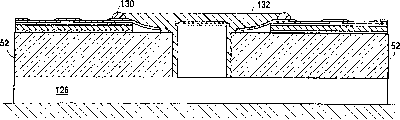
图3示出根据所揭示方法和装置的一个实施例的芯片级封装设计的截面图,在半导体模片52与包括两层柔性电路带(或柔性电路或TAB带)58的中间电路之间设置一非聚合物支承结构50。在本实施例中,非聚合物支承结构50通过粘合层64与模片52实现结构耦合。正如这里所采用的,“结构耦合”意指利用任何合适的方式(如通过淀积、采用粘合剂或其它焊接形式)使两个元件直接耦合或者间接耦合(例如,用位于二者之间的插入层或其它元件)。正如图3所示,半导体模片52通常有模片焊接片或触点84。第二粘合层56将非聚合物衬垫50附着到柔性带58上。尽管图3示出采用两层柔性电路带的芯片级封装设计的一个实施例,但是,应当明白,本公开内容的好处在于,采用其它类型的中间电路,例如具有三层或多层的非柔性电路条带或柔性电路带也是可以的。例如,图3C示出采用三层带19和引线焊接的一个实施例。在这一实施例中,三层带19包括电介质层60、导电层59和第二电介质层(通常为聚酰亚胺)60a。在层59与60a之间采用粘合层60b。
中间电路通常包括与诸如PCB的基板的电学连接的互连阵列。在图3所示的实施例中,两层柔性电路带58通常包括有图案的电介质层60和具有各个导电焊接垫片59a的有图案平面导电层59。焊球导电焊接垫片59a通常直径约在200微米至600微米之间,二者之间的间距约在300微米至1250微米之间。有图案导电层59可以由适合于形成基本平面的电路的任何可形成图案的导电材料组成,包括诸如硅和多晶硅、钨、钛、铝、基于铝的金属(如铝合金)、铜及其合金和组合等的金属或导体,但不限于此。(对于本公开内容,术语“金属”限定为包括金属、耐熔金属、金属互化物等及其组合)。最典型的有图案导电层59是铜。有图案的电介质层60可以是由适合于使导电层59绝缘的任何可形成图案的介质材料组成,包括聚酰亚胺或聚酯,但不限于此。最典型的电介质层60是聚酰亚胺,如“DUPONT KAPTON”或“UBE UPILEX”。有图案的导电层59的厚度通常约在0.5密耳至1.5密耳之间。有图案的电介质层60的厚度通常约在1密耳至3密耳之间。
为了形成球形格栅阵列57,导电焊球(或焊柱)54被附着到柔性带58上并通过在电介质层60中图案形成的开孔(或通孔)62与各个焊接垫片59a电学接触。以与各个导电焊接垫片59a互补的方式形成开孔62图案,使得每个开孔覆盖各个导电焊接垫片59a。焊球54可以是适合于通过开孔62与焊接垫片59a连接的任何形状和尺寸。通常,焊球54基本是球形的,直径约在250微米至750微米之间,最常用的约在300微米至600微米之间。焊球通常是利用诸如红外、对流或汽相的传统炉回流固定的。以这样的方式使开孔62的形状和尺寸适合于接受焊球54,即可以与焊接垫片59a相电学接触。通常,开孔62是圆形的,直径约在250微米至600微米之间,最常用的约在300微米至500微米之间。导电焊球可以由任何合适的导电材料构成,包括金、焊剂或铜,但不限于此。
在图3所示的实施例中,有图案的导电层59通常具有多个焊接引线82、每个焊接引线与导电焊接垫片59a电耦合。通常,焊接引线82的宽度约在25微米至100微米之间。引线82是通过例如内引线焊接在模片衬垫84上实现与半导体模片52的电连接,因此配置与模片衬垫84相似的间距,长度足以允许引线82与衬垫84之间的配对。然而,也可以引线82,利用图3A中所示的引线焊接82a使衬垫83引线焊接到半导体模片52上。在两种情况中,当每个焊接引线82被电学连接到各个模片84上时,在每个焊球54与相应模片衬垫84之间实现一个电路。当为形成球形格栅阵列而如此构成时,设计的每个焊球54被用作使基板76上各个模片衬垫84与相应焊接垫片75电学连接的各个“管脚”。球形格栅阵列的间距如图6所示,具有相应的基板焊接模片衬垫75,通常约在300微米至1250微米之间。通常,基板是印刷电路板(“PCB”),但是也可以是任何其它电路,包括柔性电路、硅、基片等,但不限于此。
正如图3所示,模片52和内引线连接区通常被密封剂86所密封,密封剂86放在密封封壳88内。密封剂86可以是本领域技术人员所熟知的任何合适的密封剂,包括环氧树脂和硅酮,但不限于此。密封剂封壳88可以是任何合适的密封剂存放结构,包括例如环氧树脂、粘合剂带等。尽管图3所示的实施例示出采用单层有图案的导电层59的芯片级封装设计,但是,应当明白,本发明的好处在于,实施例也可以采用两层或多层有图案(或没有图案)的导电层。
在图3的实施例中,非聚合物衬垫50可以是适当坚固以便于处理和/或热膨胀系数接近于基板热膨胀系数以使焊接点上的应力减至最小的任何材料。利用这样的非聚合物衬垫结构,可以减少或基本消除在模片附着粘合剂64中形成空隙。这是因为用粘合剂64直接将模片52焊接到非聚合物衬垫60上,因此,不存在来自聚合物材料的湿气,和不能进入这两个元件之间的接口处。
除了减小热应力和空隙形成外,所揭示的方法和装置的非聚合物衬垫结构还提供其它的重要优点。例如,包括非聚合物支承结构10的芯片级封装条带提供的表面,其平整度和表面均匀性比传统弹性体衬垫有所提高。格栅阵列支承结构表面的平整度是保证所有焊球54与基板76上衬垫75接触的一个重要因素。比较理想地,芯片级封装支承结构的共面性约为2密耳或更低,更理想地,约为1密耳或更低。这种共面性是采用传统软弹性体衬垫难以实现的。非聚合物支承结构为焊球附着提供了更平的表面,因此允许半导体模片与基板之间的连接更可靠。
除了上述的好处外,可以采用热导电非聚合物(如金属片即金属箔)作为非聚合物支承结构50,为从图3中半导体模片52的正面(或图3A中半导体模片52的背面)的热耗散提供良好的热通路。这种热导电非聚合物支承结构50还可以有效地把热传导到焊球54上。
通常采用的一种类型的热导电非聚合物是金属片即金属箔,铜是特别适合于此的金属。除了热导以外,金属片还可以改善导电层59的电屏蔽和有有助于使交扰减至最小。此外,金属片提供适合于用作接地平面的表面。因此,金属片还可以用于提供一种方便的接地平面(如果需要的话,或者是供电平面),例如通过使焊球54a与金属片53直接电连接,如图3B所示。这可以例如通过导电衬垫59b中的通孔55和下方的粘合剂层56进行,使得所选接地连接焊球54a可以与金属片53相电连接。然后,通过内引线或者通过引线焊接82b使模片中的接地衬垫与接地焊球54a连接,如图3B所示。有利地,当采用诸如铜箔的金属片时,可以用相对较低的成本获得这些优点。合适的金属片包括提供足够硬度和/或热膨胀质量的任何有图案的金属箔,包括由铜、不锈钢、合金42、钨、钛、铝、基于铝的金属(如铝合金)、和合金及其组合等制成的金属箔,但不限于此。也可以给铜箔涂覆薄的焊接镀层,提供良好的焊接能力、低的成本和/或降低氧化。合适的镀层的例子包括电镀镍、镍/硼、黑铜氧化物、锡/铅(如高于37%铅的高铅含量的锡/铅合金)、或贵金属,如银或金的表面镀层,但是不限于此。最通常地,非聚合物支持结构是厚度约在4密耳至10密耳之间的有图案的铜箔,较通常地,厚度约在5密耳至7密耳之间。铜合金通常用作引线框,如194,最适合于本应用。
当采用合适硬度的非聚合物衬垫时,用引线框常用的典型箱盒馈送设备处理芯片级封装条带可能是有利的。“合适的硬度”,这是指模量大于1Mpsi(1×10⁶每平方英寸磅)。具有合适硬度的非聚合物材料的例子包括陶瓷、和诸如上述这些的金属箔。然而,应当明白,利用模量小于约1Mpsi的非聚合物也可以实现所所揭示方法和装置的好处。这些好处包括文中别处所述的这些的好处。
参考图3,粘合剂层56和64可以是适合将非聚合物衬垫50固定到柔性带58和半导体模片52上的任何粘合剂。通常,粘合剂层56和64选自介质材料,介质材料与非聚合物衬垫50一起的的作用是具有使模片52与基板(或PCB)76相隔离或“去耦合”,因此进一步缓解焊接点上的应力和改善可靠性。这种粘合剂的作用还有为插入插座提供少量的Z轴柔量。合适的粘合剂的例子包括丙烯酸PSA、热塑性聚酰亚胺(如DuPont的“KJ”材料)、聚烯烃、DuPont公司的“PYRALUX”、环氧树脂及其混合物,但不限于此。通常采用热塑性聚酰亚胺作为粘合剂层56和64。
可以用适合于在弹性体衬垫与相邻表面,如模片或电路踪迹之间形成焊接的任何厚度将粘合剂施加于非聚合物衬垫上。通常,粘合剂层56和64的厚度约在1密耳至3密耳之间,更常用的厚度约在1密耳至2密耳之间。
尽管示出的实施例采用单个非聚合物支承结构,但是,应当理解,本发明的好处在于,在层叠的芯片级封装带组件中可以采用一个以上的非聚合物支承结构。例如,可以采用两个或多个电学隔离的金属支承结构,将其用于形成分别的电路通路(如接地平面和供电平面二者),或者金属与非金属非聚合物支承结构的组合也是可以是,如环氧树脂印刷电路板材料。
在图3D所示的另一实施例中,安装层351可以仿造淀积非聚合物材料350的层并用在半导体模片352与附属电路之间。例如,安装层351可以用粘合剂层356粘合到两层柔性电路带318或者其它中间电路上,和用粘合剂层364粘合到半导体电路芯片352上。当不是采用以上所述的非聚合物支承结构实施例时,非聚合物层350的作用是通过基本阻止湿气逃逸到模片附着粘合剂364中而降低或基本消除空隙的形成。用许多方法可以有利地制造出仿造非聚合物材料图案的安装层,包括作为单独带元件或者附着到TAB带上,但不限于此。在有些情况下,利用仿造非聚合物材料图案的安装层可能比前面所述的非聚合物支承结构的实施例更低廉。
仍参考图3D,非聚合物层350可以由适合于阻止湿气迁移到粘合剂层364中的任何非聚合物材料组成,包括为用作非聚合物支承结构而列出的这些材料。安装层351可以是适合于形成非聚合物层350图案或淀积的任何材料,包括为用作可形成图案的介电材料而列出的这些介质材料。同样,粘合剂层356和364可以是任何合适的粘合剂或附着手段,包括为供非聚合物支承结构使用而列出的这些。通常的非聚合物层350是厚度约在1微米至2微米之间的铜层,安装层351是厚度约在1密耳至3密耳之间的聚酰亚胺层。更一般地,非聚合物层350是厚度约在5微米至10微米之间的铜层,安装层351是厚度约为2密耳的聚酰亚胺层。
图3D示出在类似于图3A所示的应用中使用了仿造非聚合物层350的安装层351。与非聚合物支承结构的实施例一样,对于图3D所示的构造可以作出许多变化。例如,导电非聚合物层350可以用作接地平面、供电平面或者完成其它类型的电路通路,如以类似于图3B为非聚合物支承结构所示出的方式。安装层351和非聚合物层351也可以与具有三层或更多层的中间电路一起使用,如与图3C为非聚合物支承结构所示出的实施例相似。此外,可以采用一个以上的非聚合物层350。
芯片级封装元件的制造和组装
用许多方法可以形成具有非聚合物支承结构(或“衬垫”)的本发明所揭示方法和装置的芯片级封装器件,并将其用于许多不同应用中。例如,构造具有非聚合物衬垫的芯片级封装带的一种方法包括步骤:将粘合剂叠合到非聚合物材料(如金属箔)的滚筒上,以所需形状冲压或模压非聚合物材料,使弯曲电路(或电路踪迹)与非聚合物对准和粘合,形成芯片级封装带(例如以条带的形式)。在另一不同的方法中,通过将非聚合物材料(图金属箔)冲压成所需形状,将粘合剂薄膜冲压成相同的形状,使薄膜和箔片二者与电路踪迹对准,以及使结构叠合起来,可以形成芯片级封装带。在这两种情况中,电路踪迹与非聚合物支承结构的对准是准确的,也是比较低廉的。可以进行多种不同的步骤,利用刚才所述的芯片级封装条带或带形成芯片级封装器件。这些步骤包括:模片附着、引线和/或内引线焊接、过塑模和/或焊球附着步骤。有利地,根据这些过程的芯片级封装器件的组装是比较有效、直接和经济有效的。
图4示出粘合剂层56和64叠合到铜片(或箔)50的薄卷筒的两侧。通常,采用具有覆盖层(或防粘衬里)的粘合剂叠层,防粘衬里被留在粘合剂层56和64背离铜箔50的这一侧上。加入防粘衬里的粘合剂叠层包括丙烯酸PSA型粘合剂。如图4所示,用于形成粘合剂层56和64的叠合粘合剂通常是利用滚筒叠层100施加的。然而,应当明白,本发明的好处在于,可以利用任何的合适的方法,包括(但不限于)丝网印刷和喷洒淀积法,施加诸如前面所述的这些粘合剂。
图5示出已经与粘合剂层56和64叠合在一起的非聚合物片50的俯视图。在图5中,已经将非聚合物片50冲压或模压形成具有被连接槽区域110环绕的模片方块51的图案。模片方块51构造成具有与半导体模片52相互补的形状和更小的面积,给引线82(或者引线焊接)连接到连接槽区域110中的模片衬垫84留有间隙。连接槽110为利用内引线焊接、引线焊接或其它的合适连接方法连接到模片衬垫84上提供空间。合起来,模片方块51和连接槽110的尺寸为半导体模片52提供各个平台。
应当理解,本发明的好处在于,在所揭示的方法中模压或冲压操作可以利用任何适合于集成电路封装的任何冲压或模压方法进行。通过化学刻蚀,利用钢尺模片或利用化学刻蚀模片也可以使非聚合物形成图案。在片50中也可以冲压工具孔112,帮助电路的准确对准。
接着,如图6所示,利用工具孔112使具有接受焊球的通孔62的柔性带58对准并叠合到铜片50的一侧上。电路的叠合可以用许多方法进行,包括用滚筒-滚筒方法(如利用链齿孔的滚筒-滚筒方法)或者以压印方法。在本实施例中,通常在叠合前从粘合剂层56上撕去防粘衬里,利用对准用的工具孔,将电路的面板或条带叠合到片50上。然而,可以采用其它的粘合和叠合方法,如前面所述的方法。
此时,集成电路的附着和焊接可以不中断地继续,被附着的柔性带58可以送往别处,以供进一步组装。在后一种情况中,通常在输送前将非聚合物片50和附着的柔性带58切割成条带形式。用条带形式,单个芯片级封装条带通常具有若干个分别的模片方块51。在这两种情况中,进一步的组装通常涉及从粘合剂层64上去除第二防粘衬里,为将模片安装到非聚合物片50上作准备。在条带形式工艺的情况中,将非聚合物片的条带和附着的电路装载到处理用的料箱中。然后将模片放置在非聚合物条带的粘性侧面(与有电路的侧面相对),如果需要的话使之固化。然而,应当明白,本发明的好处在于,模片也可以被检起并放置在一卷非聚合物片上(与条带相对),半导体模片可以与其电路一起放置,与非聚合物片相邻或者相对。也可以使非聚合物条带的模片侧面留下裸露的粘合剂和模片附着粘合剂(通常为基于环氧树脂的材料),以供模片的附着使用。
接着,使条带(包括电路和一个或多个模片)倒装和放置到标准料箱中,将其装载到例如引线焊接机或者热压焊接机中。如图7所示,利用例如焊接工具124将来自带的每个引线120焊接到模片衬垫122上。利用固定器126支承柔性带(包括模片),从而使引线120在焊接过程期间在易碎部分(或刻痕)126断裂。如图8所示,然后,通过用密封剂132填充槽110可以使条带过塑模。通常,密封剂被阻挡部件130所包容,利用合适的固化方法,如紫外或热方法进行固化。或者,如图9所示,可以将条带倒装在固定器表面140上,用密封剂132从条带的模片一侧填充槽110,无需密封剂阻挡部件。正如图3A和3B所示,模片52也可以利用引线焊接82a连接到电路轨迹层59上,例如,当半导体模片是“倒装片”时,使得电路层和半导体模片的模片衬垫取向为背离支承结构的方向。图6A示出这个实施例的俯视图。
如图10所示,接着可以将焊球(或焊柱)54装在形成的开孔(或通孔)62,例如通过在聚酰亚胺层60中刻蚀的开孔中。利用适合于在球54与导电焊接衬垫59a之间形成牢固电学连接的任何方法,包括例如利用诸如红外、对流或汽相的任何传统手段进行加热和回流,可以使焊球54附着到条带上。尽管图中未示出,但是,通孔62也可以处理为电镀通孔(PTH)和/或在焊球附着前填充不同的导电填充剂材料。
此时,可以对条带或卷筒进行切割,形成单个或多个模片的芯片级封装(图10示出一个单个模片的封装150)。这可以利用诸如冲压、切割或其它类似过程的任何合适的切除方法来完成。
应当明白,本发明的好处在于,利用这一方法,可以制备其它的芯片级封装的结构,包括具有一个以上半导体模片的封装。此外,利用所公开的方法和装置概念可以制造诸如传统BGA封装的非芯片级封装的结构。还应当明白,虽然刚才所描述和示出的方法是为了利用条带形成制造集成电路,但是,当被用于利用其它过程和形式制造集成电路,包括利用滚筒-滚筒(或者卷筒-卷筒)形式形成集成电路,但不限于此,也可以获得这些方法的好处。在这方面,以与现行工业基础结构相兼容的形式和使用当前所发展的更新的形式可以实现所所揭示方法和装置的好处。还应当明白,上述的封装过程可以与仍在基片形式中的模片一起进行。例如,可以使非聚合物片对准和直接粘合到进行焊接的基片和芯片上。如前所述,然后用密封剂填充槽,附着焊球以及冲压或锯开各个封装件。
本发明可以适合于各种不同的改进和变化形式,这里,通过举例的方式已经示出并描述了具体的实施例。然而,应当明白,不希望本发明被限于所公开的具体形式。而是,本发明覆盖落在所附权利要求书中所限定的本发明的精神和范围内的所有的改进。等效和替代。
Claims (32)
1.一种集成电路的封装,其特征在于它包括:
包括电子互连阵列的中间电路;
具有第一和第二侧面的至少一层非聚合物层,所述层的第一侧面与所述集成电路相结构耦合,所述层的第二侧面与所述中间电路相结构耦合。
2.如权利要求1所述的封装,其特征在于:所述的集成电路具有多个电接触部位,所述的接触部位与所述中间电路的所述电互连相电气耦合。
3.如权利要求2所述的封装,其特征在于:所述集成电路的所述电接触部位被引线焊接到所述中间电路的所述电互连上。
4.如权利要求2所述的封装,其特征在于:所述集成电路的所述电接触部位被热压焊接到所述中间电路的所述电互连上。
5.如权利要求1所述的封装,其特征在于:所述的非聚合物层是导电的,所述的非聚合物层被电耦合到所述集成电路上,形成供电或接地平面。
6.如权利要求1所述的封装,其特征在于:所述的非聚合物层是模量大于约1Mpsi的非聚合物支承结构。
7.如权利要求1所述的封装,其特征在于:所述的非聚合物层是由厚度约在4密耳至10密耳之间的金属箔组成的非聚合物支承结构。
8.如权利要求1所述的封装,其特征在于:所述的非聚合物层是由铜箔组成的非聚合物支承结构。
9.如权利要求1所述的封装,其特征在于进一步包括具有第一和第二侧的安装层,所述安装层的第一侧面与所述非聚合物层的第二侧面相结构耦合,所述安装层的第二侧面与所述中间电路相结构耦合。
10.如权利要求9所述的封装,其特征在于:所述的安装层是厚度约在1密耳至3密耳之间的聚酰亚胺层,所述的非聚合物层是厚度约在1微米至20微米之间的铜层。
11.如权利要求1所述的封装,其特征在于:所述的中间电路是柔性电路。
12.如权利要求1所述的封装,其特征在于:所述的中间电路具有第一和第二侧面,所述中间电路的第一侧面与所述非聚合物层的第二侧面相结构耦合;和
进一步包括多个与所述中间电路相电气耦合的焊球或焊柱;所述的多个焊球或焊柱与所述中间电路的第二侧面相结构耦合。
13.一种形成集成电路封装的方法,其特征在于,所述方法包括步骤:
提供一包括电学互连阵列的中间电路;
提供具有第一和第二侧面的至少一层非聚合物层;所述非聚合物层的第一侧面适合于与所述集成电路相结构耦合;和
将所述非聚合物层的第二侧面结构耦合到所述中间电路上。
14.如权利要求13所述的方法,其特征在于进一步包括将所述集成电路在结构上耦合到所述非聚合物层的所述第一侧面上的步骤。
15.如权利要求14所述的方法,其特征在于:所述的集成电路具有多个电接触部位,进一步包括将所述接触部位在电学上耦合到所述中间电路的所述电学互连上的步骤。
16.如权利要求14所述的方法,其特征在于:把所述接触部位电学耦合到所述电学互连上的步骤包括把所述集成电路的所述接触部位引线焊接或者热压焊接到所述中间电路的所述电学互连上的步骤。
17.如权利要求14所述的方法,其特征在于:所述的非聚合物层是导电的,进一步包括把所述非聚合物支承结构电耦合到所述集成电路上,形成供电和接地平面的步骤。
18.如权利要求13所述的方法,其特征在于:所述的非聚合物层是模量大于约1Mpsi的非聚合物支承结构。
19.如权利要求13所述的方法,其特征在于:所述的非聚合物层是非聚合物支承结构,是厚度约在4密耳至10密耳之间的金属箔。
20.如权利要求13所述的方法,其特征在于:所述的非聚合物层是包括铜箔的非聚合物支承结构。
21.如权利要求13所述的方法,其特征在于:所述的非聚合物层是厚度约在1微米至20微米之间的铜层。
22.如权利要求13所述的方法,其特征在于:所述的中间电路是柔性电路。
23.如权利要求13所述的方法,其特征在于:所述的中间电路具有第一和第二侧面;将所述中间电路结构耦合到所述非聚合物层的所述步骤包括把所述中间电路的第一侧面在结构上连接到所述非聚合物层的第二侧面的步骤;和进一步包括将多个焊球或焊柱电耦合到所述中间电路的步骤;所述的多个焊球或焊柱被结构耦合到所述中间电路的所述第二侧面。
24.一种电子封装,其特征在于它包括:
包括一层有图案的导电层和至少一层有图案的电介质层的柔性带;
具有第一和第二侧面的非聚合物支承结构,所述支承结构的第一侧面被结构耦合到所述柔性带的所述导电层的第二侧面上。
25.如权利要求24所述的封装,其特征在于:所述导电层具有第一和第二侧面并印制图案以形成导电区域,所述电介质层具有第一和第二侧面并进行图案处理以形成穿过所述电介质层延伸的多个开孔,所述开孔中的每一个被配置为接收一个焊球,这里所述导电层的第一侧面被连接到所述电介质层的第二侧面,从而使所述电介质层中的所述多个开孔与所述导电层的至少部分所述导电区域相对准。
26.如权利要求25所述的封装,其特征在于进一步包括其第一侧面被结构耦合到所述非聚合物支承结构的第二侧面的半导体器件,所述半导体器件包括多个电接触部位,所述的接触部位被电耦合到所述柔性带的所述导电层上。
27.如权利要求26所述的封装,其特征在于进一步包括设置在所述柔性带的所述电介质层的第一侧面上的多个焊球或焊柱,所述焊球或焊柱中的每一个被定位在所述电介质层中所述多个开孔的一个开孔中并被电连接到所述柔性带的所述导电层的所述导电区上。
28.如权利要求27所述的封装,其特征在于:所述的非聚合物支承结构的模量大于约1Mpsi。
29.如权利要求27所述的封装,其特征在于:所述的非聚合物支承结构是厚度约在4密耳至10密耳之间的铜箔。
30.一种电子封装,其特征在于它包括:
具有第一和第二侧面和一个外侧边界的有图案导电层,对所述导电层进行图案化以形成环绕所述外侧边界的圆周设置周边导电特征的导电区域,作为半导体器件的电连接;
具有第一和第二侧面和圆周小于所述有图案导电层的所述圆周的外侧边界的有图案电介质层,对所述电介质层进行图案化以形成穿过所述电介质层延伸的多个开孔,所述开孔中的每一个开孔被设置为接收一个焊球,这里,所述导电层的第一侧面被连接到所述电介质层的第二侧面,以致于所述电介质层中的所述多个开孔与所述导电层的至少部分所述导电区域相对准,所述导电层的所述周边导电特征延伸到所述介质构件的外侧边界以外;
具有第一和第二侧面的非聚合物支承结构,所述支承结构是基本坚固的和具有大于约1Mpsi的弹性模量,所述支承结构的第一侧面被结构耦合到所述导电层的第二侧面上;
具有第一侧面的半导体器件,所述第一侧面被结构耦合到所述非聚合物支承结构的第二侧面上,所述半导体器件包括多个电接触部位,所述接触部位中至少有一个被电耦合到所述导电层的所述周边导电特征上;以及
设置在所述电介质层的第一侧面上的多个焊球,所述焊球中的每一个被定位在所述电介质层中所述多个开孔的一个开孔中并被电连接到所述导电层的所述导电区上。
31.如权利要求30所述的封装,其特征在于:所述半导体器件的所述电接触部位是采用引线焊接、内引线或其组合的手段电耦合到所述导电层的所述周边导电特征上。
32.如权利要求30所述的封装,其特征在于:所述非聚合物支承结构是导电的,所述非聚合物支承结构被电耦合在所述半导体器件的所述电接触部位中至少一个部位与所述导电层之间,使得所述非聚合物支承结构在所述半导体器件与所述导电层之间形成电气电路。
Applications Claiming Priority (2)
| Application Number | Priority Date | Filing Date | Title |
|---|---|---|---|
| US08/759,253 | 1996-12-02 | ||
| US08/759,253 US5990545A (en) | 1996-12-02 | 1996-12-02 | Chip scale ball grid array for integrated circuit package |
Publications (1)
| Publication Number | Publication Date |
|---|---|
| CN1239589A true CN1239589A (zh) | 1999-12-22 |
Family
ID=25054972
Family Applications (1)
| Application Number | Title | Priority Date | Filing Date |
|---|---|---|---|
| CN97180210A Pending CN1239589A (zh) | 1996-12-02 | 1997-04-02 | 集成电路封装用的芯片级球形格栅阵列 |
Country Status (12)
| Country | Link |
|---|---|
| US (1) | US5990545A (zh) |
| EP (1) | EP0948814B1 (zh) |
| JP (1) | JP2001506057A (zh) |
| KR (1) | KR100532179B1 (zh) |
| CN (1) | CN1239589A (zh) |
| AT (1) | ATE273564T1 (zh) |
| AU (1) | AU2435397A (zh) |
| CA (1) | CA2272434A1 (zh) |
| DE (1) | DE69730239D1 (zh) |
| HK (1) | HK1023225A1 (zh) |
| MY (1) | MY119341A (zh) |
| WO (1) | WO1998025303A1 (zh) |
Cited By (2)
| Publication number | Priority date | Publication date | Assignee | Title |
|---|---|---|---|---|
| CN108122873A (zh) * | 2016-11-28 | 2018-06-05 | 日月光半导体制造股份有限公司 | 包括填充模制连通柱的半导体器件封装 |
| CN112180128A (zh) * | 2020-09-29 | 2021-01-05 | 西安微电子技术研究所 | 一种带弹性导电微凸点的互连基板和基于其的kgd插座 |
Families Citing this family (89)
| Publication number | Priority date | Publication date | Assignee | Title |
|---|---|---|---|---|
| JP2891665B2 (ja) | 1996-03-22 | 1999-05-17 | 株式会社日立製作所 | 半導体集積回路装置およびその製造方法 |
| US20040061220A1 (en) * | 1996-03-22 | 2004-04-01 | Chuichi Miyazaki | Semiconductor device and manufacturing method thereof |
| JP3195236B2 (ja) | 1996-05-30 | 2001-08-06 | 株式会社日立製作所 | 接着フィルムを有する配線テープ,半導体装置及び製造方法 |
| US6962829B2 (en) * | 1996-10-31 | 2005-11-08 | Amkor Technology, Inc. | Method of making near chip size integrated circuit package |
| US6150193A (en) * | 1996-10-31 | 2000-11-21 | Amkor Technology, Inc. | RF shielded device |
| US5981314A (en) | 1996-10-31 | 1999-11-09 | Amkor Technology, Inc. | Near chip size integrated circuit package |
| DE69830883T2 (de) * | 1997-03-10 | 2006-04-20 | Seiko Epson Corp. | Halbleiterbauelement und mit diesem Bauelement bestückte Leiterplatte |
| JP3301355B2 (ja) * | 1997-07-30 | 2002-07-15 | 日立電線株式会社 | 半導体装置、半導体装置用tabテープ及びその製造方法、並びに半導体装置の製造方法 |
| US5888850A (en) * | 1997-09-29 | 1999-03-30 | International Business Machines Corporation | Method for providing a protective coating and electronic package utilizing same |
| US6310298B1 (en) * | 1997-12-30 | 2001-10-30 | Intel Corporation | Printed circuit board substrate having solder mask-free edges |
| US6574858B1 (en) | 1998-02-13 | 2003-06-10 | Micron Technology, Inc. | Method of manufacturing a chip package |
| JP3481117B2 (ja) * | 1998-02-25 | 2003-12-22 | 富士通株式会社 | 半導体装置及びその製造方法 |
| US6166433A (en) * | 1998-03-26 | 2000-12-26 | Fujitsu Limited | Resin molded semiconductor device and method of manufacturing semiconductor package |
| US6265776B1 (en) * | 1998-04-27 | 2001-07-24 | Fry's Metals, Inc. | Flip chip with integrated flux and underfill |
| US6089920A (en) * | 1998-05-04 | 2000-07-18 | Micron Technology, Inc. | Modular die sockets with flexible interconnects for packaging bare semiconductor die |
| WO2000005765A1 (de) * | 1998-07-22 | 2000-02-03 | Dyconex Patente Ag | Verfahren zur herstellung von umverdrahtungssubstraten für halbleiterchippackungen |
| US6479887B1 (en) | 1998-08-31 | 2002-11-12 | Amkor Technology, Inc. | Circuit pattern tape for wafer-scale production of chip size semiconductor packages |
| US6428641B1 (en) | 1998-08-31 | 2002-08-06 | Amkor Technology, Inc. | Method for laminating circuit pattern tape on semiconductor wafer |
| KR20010099684A (ko) | 1998-10-14 | 2001-11-09 | 스프레이그 로버트 월터 | 상호 연결된 접지면이 있는 테이프 볼 그리드 어레이 |
| JP2000138317A (ja) | 1998-10-31 | 2000-05-16 | Anam Semiconductor Inc | 半導体装置及びその製造方法 |
| JP2000138262A (ja) | 1998-10-31 | 2000-05-16 | Anam Semiconductor Inc | チップスケ―ル半導体パッケ―ジ及びその製造方法 |
| TW434850B (en) * | 1998-12-31 | 2001-05-16 | World Wiser Electronics Inc | Packaging equipment and method for integrated circuit |
| US6175160B1 (en) * | 1999-01-08 | 2001-01-16 | Intel Corporation | Flip-chip having an on-chip cache memory |
| US6377464B1 (en) * | 1999-01-29 | 2002-04-23 | Conexant Systems, Inc. | Multiple chip module with integrated RF capabilities |
| US6341418B1 (en) | 1999-04-29 | 2002-01-29 | International Business Machines Corporation | Method for direct chip attach by solder bumps and an underfill layer |
| US6191483B1 (en) * | 1999-05-06 | 2001-02-20 | Philips Electronics North America Corporation | Package structure for low cost and ultra thin chip scale package |
| JP3397725B2 (ja) * | 1999-07-07 | 2003-04-21 | 沖電気工業株式会社 | 半導体装置、その製造方法及び半導体素子実装用テープの製造方法 |
| JP3521325B2 (ja) * | 1999-07-30 | 2004-04-19 | シャープ株式会社 | 樹脂封止型半導体装置の製造方法 |
| US6285077B1 (en) * | 1999-08-19 | 2001-09-04 | Lsi Logic Corporation | Multiple layer tape ball grid array package |
| JP2001156212A (ja) * | 1999-09-16 | 2001-06-08 | Nec Corp | 樹脂封止型半導体装置及びその製造方法 |
| US6656765B1 (en) | 2000-02-02 | 2003-12-02 | Amkor Technology, Inc. | Fabricating very thin chip size semiconductor packages |
| US6560108B2 (en) * | 2000-02-16 | 2003-05-06 | Hughes Electronics Corporation | Chip scale packaging on CTE matched printed wiring boards |
| US6686652B1 (en) | 2000-03-20 | 2004-02-03 | National Semiconductor | Locking lead tips and die attach pad for a leadless package apparatus and method |
| US6452255B1 (en) | 2000-03-20 | 2002-09-17 | National Semiconductor, Corp. | Low inductance leadless package |
| US6372539B1 (en) | 2000-03-20 | 2002-04-16 | National Semiconductor Corporation | Leadless packaging process using a conductive substrate |
| US6399415B1 (en) * | 2000-03-20 | 2002-06-04 | National Semiconductor Corporation | Electrical isolation in panels of leadless IC packages |
| DE10014380A1 (de) * | 2000-03-23 | 2001-10-04 | Infineon Technologies Ag | Vorrichtung zum Verpacken von elektronischen Bauteilen |
| US6444499B1 (en) * | 2000-03-30 | 2002-09-03 | Amkor Technology, Inc. | Method for fabricating a snapable multi-package array substrate, snapable multi-package array and snapable packaged electronic components |
| US6320137B1 (en) * | 2000-04-11 | 2001-11-20 | 3M Innovative Properties Company | Flexible circuit with coverplate layer and overlapping protective layer |
| TW466720B (en) * | 2000-05-22 | 2001-12-01 | Siliconware Precision Industries Co Ltd | Semiconductor package with flash-prevention structure and manufacture method |
| US6501170B1 (en) | 2000-06-09 | 2002-12-31 | Micron Technology, Inc. | Substrates and assemblies including pre-applied adhesion promoter |
| US6710456B1 (en) * | 2000-08-31 | 2004-03-23 | Micron Technology, Inc. | Composite interposer for BGA packages |
| JP4570809B2 (ja) * | 2000-09-04 | 2010-10-27 | 富士通セミコンダクター株式会社 | 積層型半導体装置及びその製造方法 |
| US6624005B1 (en) | 2000-09-06 | 2003-09-23 | Amkor Technology, Inc. | Semiconductor memory cards and method of making same |
| US6809935B1 (en) | 2000-10-10 | 2004-10-26 | Megic Corporation | Thermally compliant PCB substrate for the application of chip scale packages |
| US6552436B2 (en) * | 2000-12-08 | 2003-04-22 | Motorola, Inc. | Semiconductor device having a ball grid array and method therefor |
| DE10064691A1 (de) * | 2000-12-22 | 2002-07-04 | Infineon Technologies Ag | Elektronisches Bauteil mit einem Halbleiter-Chip und Kupferleiterbahnen auf dem Chip sowie ein Verfahren zu seiner Herstellung |
| US6770963B1 (en) | 2001-01-04 | 2004-08-03 | Broadcom Corporation | Multi-power ring chip scale package for system level integration |
| DE10120408B4 (de) * | 2001-04-25 | 2006-02-02 | Infineon Technologies Ag | Elektronisches Bauteil mit einem Halbleiterchip, elektronische Baugruppe aus gestapelten Halbleiterchips und Verfahren zu deren Herstellung |
| US7115986B2 (en) | 2001-05-02 | 2006-10-03 | Micron Technology, Inc. | Flexible ball grid array chip scale packages |
| EP1280204A3 (en) * | 2001-06-27 | 2004-09-01 | Shinko Electric Industries Co. Ltd. | Wiring substrate having position problem |
| US6793759B2 (en) * | 2001-10-09 | 2004-09-21 | Dow Corning Corporation | Method for creating adhesion during fabrication of electronic devices |
| US6873059B2 (en) * | 2001-11-13 | 2005-03-29 | Texas Instruments Incorporated | Semiconductor package with metal foil attachment film |
| US6664615B1 (en) * | 2001-11-20 | 2003-12-16 | National Semiconductor Corporation | Method and apparatus for lead-frame based grid array IC packaging |
| US6657134B2 (en) | 2001-11-30 | 2003-12-02 | Honeywell International Inc. | Stacked ball grid array |
| SG104291A1 (en) * | 2001-12-08 | 2004-06-21 | Micron Technology Inc | Die package |
| SG104293A1 (en) | 2002-01-09 | 2004-06-21 | Micron Technology Inc | Elimination of rdl using tape base flip chip on flex for die stacking |
| SG115455A1 (en) | 2002-03-04 | 2005-10-28 | Micron Technology Inc | Methods for assembly and packaging of flip chip configured dice with interposer |
| SG111935A1 (en) * | 2002-03-04 | 2005-06-29 | Micron Technology Inc | Interposer configured to reduce the profiles of semiconductor device assemblies and packages including the same and methods |
| SG115456A1 (en) | 2002-03-04 | 2005-10-28 | Micron Technology Inc | Semiconductor die packages with recessed interconnecting structures and methods for assembling the same |
| SG121707A1 (en) | 2002-03-04 | 2006-05-26 | Micron Technology Inc | Method and apparatus for flip-chip packaging providing testing capability |
| US6975035B2 (en) | 2002-03-04 | 2005-12-13 | Micron Technology, Inc. | Method and apparatus for dielectric filling of flip chip on interposer assembly |
| SG115459A1 (en) | 2002-03-04 | 2005-10-28 | Micron Technology Inc | Flip chip packaging using recessed interposer terminals |
| US7132173B2 (en) * | 2002-06-28 | 2006-11-07 | Advanced Bionics Corporation | Self-centering braze assembly |
| US20040036170A1 (en) | 2002-08-20 | 2004-02-26 | Lee Teck Kheng | Double bumping of flexible substrate for first and second level interconnects |
| US6921975B2 (en) * | 2003-04-18 | 2005-07-26 | Freescale Semiconductor, Inc. | Circuit device with at least partial packaging, exposed active surface and a voltage reference plane |
| US7266869B2 (en) * | 2003-07-30 | 2007-09-11 | Kyocera Corporation | Method for manufacturing a piezoelectric oscillator |
| US20050056946A1 (en) * | 2003-09-16 | 2005-03-17 | Cookson Electronics, Inc. | Electrical circuit assembly with improved shock resistance |
| JP3929966B2 (ja) * | 2003-11-25 | 2007-06-13 | 新光電気工業株式会社 | 半導体装置及びその製造方法 |
| US7075016B2 (en) * | 2004-02-18 | 2006-07-11 | Taiwan Semiconductor Manufacturing Co., Ltd. | Underfilling efficiency by modifying the substrate design of flip chips |
| US11081370B2 (en) * | 2004-03-23 | 2021-08-03 | Amkor Technology Singapore Holding Pte. Ltd. | Methods of manufacturing an encapsulated semiconductor device |
| DE102004020580A1 (de) * | 2004-04-27 | 2005-11-17 | Infineon Technologies Ag | Verfahren zur Herstellung eines BGA-Chipmoduls und BGA-Chipmodul |
| US7071559B2 (en) * | 2004-07-16 | 2006-07-04 | International Business Machines Corporation | Design of beol patterns to reduce the stresses on structures below chip bondpads |
| US8125076B2 (en) * | 2004-11-12 | 2012-02-28 | Stats Chippac Ltd. | Semiconductor package system with substrate heat sink |
| JP4343117B2 (ja) * | 2005-01-07 | 2009-10-14 | 株式会社ルネサステクノロジ | 半導体装置およびその製造方法 |
| US7968371B2 (en) * | 2005-02-01 | 2011-06-28 | Stats Chippac Ltd. | Semiconductor package system with cavity substrate |
| US7316572B2 (en) * | 2005-02-03 | 2008-01-08 | International Business Machines Corporation | Compliant electrical contacts |
| US20070018308A1 (en) * | 2005-04-27 | 2007-01-25 | Albert Schott | Electronic component and electronic configuration |
| JP4548264B2 (ja) * | 2005-08-01 | 2010-09-22 | 株式会社デンソー | 車両用交流発電機 |
| DE102006015222B4 (de) * | 2006-03-30 | 2018-01-04 | Robert Bosch Gmbh | QFN-Gehäuse mit optimierter Anschlussflächengeometrie |
| US7788960B2 (en) * | 2006-10-27 | 2010-09-07 | Cummins Filtration Ip, Inc. | Multi-walled tube and method of manufacture |
| US7573131B2 (en) * | 2006-10-27 | 2009-08-11 | Compass Technology Co., Ltd. | Die-up integrated circuit package with grounded stiffener |
| TWI352406B (en) * | 2006-11-16 | 2011-11-11 | Nan Ya Printed Circuit Board Corp | Embedded chip package with improved heat dissipati |
| US7944029B2 (en) * | 2009-09-16 | 2011-05-17 | Sandisk Corporation | Non-volatile memory with reduced mobile ion diffusion |
| JP5642473B2 (ja) * | 2010-09-22 | 2014-12-17 | セイコーインスツル株式会社 | Bga半導体パッケージおよびその製造方法 |
| US9159649B2 (en) * | 2011-12-20 | 2015-10-13 | Intel Corporation | Microelectronic package and stacked microelectronic assembly and computing system containing same |
| TWI544583B (zh) * | 2012-04-18 | 2016-08-01 | 鴻海精密工業股份有限公司 | 晶片組裝結構及晶片組裝方法 |
| TWI480989B (zh) | 2012-10-02 | 2015-04-11 | 矽品精密工業股份有限公司 | 半導體封裝件及其製法 |
| US20160317068A1 (en) * | 2015-04-30 | 2016-11-03 | Verily Life Sciences Llc | Electronic devices with encapsulating silicone based adhesive |
Family Cites Families (22)
| Publication number | Priority date | Publication date | Assignee | Title |
|---|---|---|---|---|
| FR2439478A1 (fr) * | 1978-10-19 | 1980-05-16 | Cii Honeywell Bull | Boitier plat pour dispositifs a circuits integres |
| US5148265A (en) * | 1990-09-24 | 1992-09-15 | Ist Associates, Inc. | Semiconductor chip assemblies with fan-in leads |
| US5148266A (en) * | 1990-09-24 | 1992-09-15 | Ist Associates, Inc. | Semiconductor chip assemblies having interposer and flexible lead |
| US5216278A (en) * | 1990-12-04 | 1993-06-01 | Motorola, Inc. | Semiconductor device having a pad array carrier package |
| US5241133A (en) * | 1990-12-21 | 1993-08-31 | Motorola, Inc. | Leadless pad array chip carrier |
| JPH05160292A (ja) * | 1991-06-06 | 1993-06-25 | Toshiba Corp | 多層パッケージ |
| US5311059A (en) * | 1992-01-24 | 1994-05-10 | Motorola, Inc. | Backplane grounding for flip-chip integrated circuit |
| US5214845A (en) * | 1992-05-11 | 1993-06-01 | Micron Technology, Inc. | Method for producing high speed integrated circuits |
| US5592025A (en) * | 1992-08-06 | 1997-01-07 | Motorola, Inc. | Pad array semiconductor device |
| US5468994A (en) * | 1992-12-10 | 1995-11-21 | Hewlett-Packard Company | High pin count package for semiconductor device |
| US5420460A (en) * | 1993-08-05 | 1995-05-30 | Vlsi Technology, Inc. | Thin cavity down ball grid array package based on wirebond technology |
| US5397921A (en) * | 1993-09-03 | 1995-03-14 | Advanced Semiconductor Assembly Technology | Tab grid array |
| US5477611A (en) * | 1993-09-20 | 1995-12-26 | Tessera, Inc. | Method of forming interface between die and chip carrier |
| US5548091A (en) * | 1993-10-26 | 1996-08-20 | Tessera, Inc. | Semiconductor chip connection components with adhesives and methods for bonding to the chip |
| US5473512A (en) * | 1993-12-16 | 1995-12-05 | At&T Corp. | Electronic device package having electronic device boonded, at a localized region thereof, to circuit board |
| TW258829B (zh) * | 1994-01-28 | 1995-10-01 | Ibm | |
| EP0751561A4 (en) * | 1994-03-18 | 1997-05-07 | Hitachi Chemical Co Ltd | PROCESS FOR MANUFACTURING SEMICONDUCTOR PACKAGES AND SEMICONDUCTOR PACKAGES |
| US5741729A (en) * | 1994-07-11 | 1998-04-21 | Sun Microsystems, Inc. | Ball grid array package for an integrated circuit |
| JP2616565B2 (ja) * | 1994-09-12 | 1997-06-04 | 日本電気株式会社 | 電子部品組立体 |
| US5528083A (en) * | 1994-10-04 | 1996-06-18 | Sun Microsystems, Inc. | Thin film chip capacitor for electrical noise reduction in integrated circuits |
| JP3123638B2 (ja) * | 1995-09-25 | 2001-01-15 | 株式会社三井ハイテック | 半導体装置 |
| US5674785A (en) * | 1995-11-27 | 1997-10-07 | Micron Technology, Inc. | Method of producing a single piece package for semiconductor die |
-
1996
- 1996-12-02 US US08/759,253 patent/US5990545A/en not_active Expired - Fee Related
-
1997
- 1997-04-02 WO PCT/US1997/005489 patent/WO1998025303A1/en active IP Right Grant
- 1997-04-02 AU AU24353/97A patent/AU2435397A/en not_active Abandoned
- 1997-04-02 DE DE69730239T patent/DE69730239D1/de not_active Expired - Lifetime
- 1997-04-02 EP EP97920070A patent/EP0948814B1/en not_active Expired - Lifetime
- 1997-04-02 JP JP52554098A patent/JP2001506057A/ja active Pending
- 1997-04-02 CN CN97180210A patent/CN1239589A/zh active Pending
- 1997-04-02 CA CA002272434A patent/CA2272434A1/en not_active Abandoned
- 1997-04-02 AT AT97920070T patent/ATE273564T1/de not_active IP Right Cessation
- 1997-04-02 KR KR10-1999-7004813A patent/KR100532179B1/ko not_active IP Right Cessation
- 1997-11-28 MY MYPI97005743A patent/MY119341A/en unknown
-
2000
- 2000-04-10 HK HK00102180A patent/HK1023225A1/xx not_active IP Right Cessation
Cited By (3)
| Publication number | Priority date | Publication date | Assignee | Title |
|---|---|---|---|---|
| CN108122873A (zh) * | 2016-11-28 | 2018-06-05 | 日月光半导体制造股份有限公司 | 包括填充模制连通柱的半导体器件封装 |
| CN112180128A (zh) * | 2020-09-29 | 2021-01-05 | 西安微电子技术研究所 | 一种带弹性导电微凸点的互连基板和基于其的kgd插座 |
| CN112180128B (zh) * | 2020-09-29 | 2023-08-01 | 珠海天成先进半导体科技有限公司 | 一种带弹性导电微凸点的互连基板和基于其的kgd插座 |
Also Published As
| Publication number | Publication date |
|---|---|
| EP0948814A1 (en) | 1999-10-13 |
| JP2001506057A (ja) | 2001-05-08 |
| HK1023225A1 (en) | 2000-09-01 |
| EP0948814B1 (en) | 2004-08-11 |
| CA2272434A1 (en) | 1998-06-11 |
| WO1998025303A1 (en) | 1998-06-11 |
| AU2435397A (en) | 1998-06-29 |
| KR20000057332A (ko) | 2000-09-15 |
| DE69730239D1 (de) | 2004-09-16 |
| KR100532179B1 (ko) | 2005-12-01 |
| US5990545A (en) | 1999-11-23 |
| MY119341A (en) | 2005-05-31 |
| ATE273564T1 (de) | 2004-08-15 |
Similar Documents
| Publication | Publication Date | Title |
|---|---|---|
| CN1239589A (zh) | 集成电路封装用的芯片级球形格栅阵列 | |
| CN1274474A (zh) | 集成电路封装用的芯片级球形格栅阵列 | |
| JP3598060B2 (ja) | 回路部品内蔵モジュール及びその製造方法並びに無線装置 | |
| US7948076B2 (en) | Semiconductor chip assembly with post/base heat spreader and vertical signal routing | |
| US7888174B2 (en) | Embedded chip package process | |
| CN1230894C (zh) | 半导体封装及其制造方法 | |
| JP5198265B2 (ja) | 薄型可撓性基板の平坦な表面を形成する装置及び方法 | |
| CN1352804A (zh) | 高密度电子封装及其制造方法 | |
| JP2008103615A (ja) | 電子部品搭載多層配線基板及びその製造方法 | |
| US7951622B2 (en) | Method of making a semiconductor chip assembly with a post/base heat spreader and a signal post | |
| CN1674277A (zh) | 电路装置 | |
| KR20010014930A (ko) | 반도체장치 | |
| US20020100969A1 (en) | Flip chip package with improved cap design and process for making thereof | |
| CN1207583A (zh) | 半导体装置和用于半导体装置的布线带 | |
| CN1591841A (zh) | 带式电路基板及使用该带式电路基板的半导体芯片封装 | |
| US6489668B1 (en) | Semiconductor device and method for manufacturing the same | |
| JP4939916B2 (ja) | 多層プリント配線板およびその製造方法 | |
| JP2012074497A (ja) | 回路基板 | |
| CN1193417C (zh) | 电路装置的制造方法 | |
| CN112701055B (zh) | 一种埋置元件的封装方法及封装结构 | |
| TW201110250A (en) | Package substrate structure and method of forming same | |
| JP2003318234A (ja) | 電子部品および電子部品の製造方法 | |
| CN101064259A (zh) | 半导体封装件及其芯片承载结构与制法 | |
| JP2004006954A (ja) | 半導体装置 | |
| JP2008172176A (ja) | 半導体素子搭載基板及びその製造方法。 |
Legal Events
| Date | Code | Title | Description |
|---|---|---|---|
| C06 | Publication | ||
| PB01 | Publication | ||
| C10 | Entry into substantive examination | ||
| SE01 | Entry into force of request for substantive examination | ||
| C02 | Deemed withdrawal of patent application after publication (patent law 2001) | ||
| WD01 | Invention patent application deemed withdrawn after publication | ||
| REG | Reference to a national code |
Ref country code: HK Ref legal event code: GR Ref document number: 1071389 Country of ref document: HK |