DE10023379B4 - Membrane probes and membrane probe assemblies, methods of making the same, and test methods used therewith - Google Patents
Membrane probes and membrane probe assemblies, methods of making the same, and test methods used therewith Download PDFInfo
- Publication number
- DE10023379B4 DE10023379B4 DE10023379A DE10023379A DE10023379B4 DE 10023379 B4 DE10023379 B4 DE 10023379B4 DE 10023379 A DE10023379 A DE 10023379A DE 10023379 A DE10023379 A DE 10023379A DE 10023379 B4 DE10023379 B4 DE 10023379B4
- Authority
- DE
- Germany
- Prior art keywords
- contact
- membrane
- sensor assembly
- substrate
- contacts
- Prior art date
- Legal status (The legal status is an assumption and is not a legal conclusion. Google has not performed a legal analysis and makes no representation as to the accuracy of the status listed.)
- Expired - Fee Related
Links
Images


Classifications
-
- H—ELECTRICITY
- H01—ELECTRIC ELEMENTS
- H01L—SEMICONDUCTOR DEVICES NOT COVERED BY CLASS H10
- H01L22/00—Testing or measuring during manufacture or treatment; Reliability measurements, i.e. testing of parts without further processing to modify the parts as such; Structural arrangements therefor
-
- G—PHYSICS
- G01—MEASURING; TESTING
- G01R—MEASURING ELECTRIC VARIABLES; MEASURING MAGNETIC VARIABLES
- G01R1/00—Details of instruments or arrangements of the types included in groups G01R5/00 - G01R13/00 and G01R31/00
- G01R1/02—General constructional details
- G01R1/06—Measuring leads; Measuring probes
- G01R1/067—Measuring probes
- G01R1/06711—Probe needles; Cantilever beams; "Bump" contacts; Replaceable probe pins
- G01R1/06733—Geometry aspects
- G01R1/06744—Microprobes, i.e. having dimensions as IC details
-
- G—PHYSICS
- G01—MEASURING; TESTING
- G01R—MEASURING ELECTRIC VARIABLES; MEASURING MAGNETIC VARIABLES
- G01R1/00—Details of instruments or arrangements of the types included in groups G01R5/00 - G01R13/00 and G01R31/00
- G01R1/02—General constructional details
- G01R1/06—Measuring leads; Measuring probes
- G01R1/067—Measuring probes
- G01R1/06711—Probe needles; Cantilever beams; "Bump" contacts; Replaceable probe pins
- G01R1/06733—Geometry aspects
- G01R1/06738—Geometry aspects related to tip portion
-
- G—PHYSICS
- G01—MEASURING; TESTING
- G01R—MEASURING ELECTRIC VARIABLES; MEASURING MAGNETIC VARIABLES
- G01R1/00—Details of instruments or arrangements of the types included in groups G01R5/00 - G01R13/00 and G01R31/00
- G01R1/02—General constructional details
- G01R1/06—Measuring leads; Measuring probes
- G01R1/067—Measuring probes
- G01R1/073—Multiple probes
- G01R1/07307—Multiple probes with individual probe elements, e.g. needles, cantilever beams or bump contacts, fixed in relation to each other, e.g. bed of nails fixture or probe card
- G01R1/0735—Multiple probes with individual probe elements, e.g. needles, cantilever beams or bump contacts, fixed in relation to each other, e.g. bed of nails fixture or probe card arranged on a flexible frame or film
-
- G—PHYSICS
- G01—MEASURING; TESTING
- G01R—MEASURING ELECTRIC VARIABLES; MEASURING MAGNETIC VARIABLES
- G01R3/00—Apparatus or processes specially adapted for the manufacture or maintenance of measuring instruments, e.g. of probe tips
-
- H—ELECTRICITY
- H05—ELECTRIC TECHNIQUES NOT OTHERWISE PROVIDED FOR
- H05K—PRINTED CIRCUITS; CASINGS OR CONSTRUCTIONAL DETAILS OF ELECTRIC APPARATUS; MANUFACTURE OF ASSEMBLAGES OF ELECTRICAL COMPONENTS
- H05K3/00—Apparatus or processes for manufacturing printed circuits
- H05K3/40—Forming printed elements for providing electric connections to or between printed circuits
- H05K3/4007—Surface contacts, e.g. bumps
-
- H—ELECTRICITY
- H05—ELECTRIC TECHNIQUES NOT OTHERWISE PROVIDED FOR
- H05K—PRINTED CIRCUITS; CASINGS OR CONSTRUCTIONAL DETAILS OF ELECTRIC APPARATUS; MANUFACTURE OF ASSEMBLAGES OF ELECTRICAL COMPONENTS
- H05K2201/00—Indexing scheme relating to printed circuits covered by H05K1/00
- H05K2201/03—Conductive materials
- H05K2201/0332—Structure of the conductor
- H05K2201/0364—Conductor shape
- H05K2201/0367—Metallic bump or raised conductor not used as solder bump
-
- H—ELECTRICITY
- H05—ELECTRIC TECHNIQUES NOT OTHERWISE PROVIDED FOR
- H05K—PRINTED CIRCUITS; CASINGS OR CONSTRUCTIONAL DETAILS OF ELECTRIC APPARATUS; MANUFACTURE OF ASSEMBLAGES OF ELECTRICAL COMPONENTS
- H05K2201/00—Indexing scheme relating to printed circuits covered by H05K1/00
- H05K2201/09—Shape and layout
- H05K2201/09209—Shape and layout details of conductors
- H05K2201/09654—Shape and layout details of conductors covering at least two types of conductors provided for in H05K2201/09218 - H05K2201/095
- H05K2201/09736—Varying thickness of a single conductor; Conductors in the same plane having different thicknesses
-
- H—ELECTRICITY
- H05—ELECTRIC TECHNIQUES NOT OTHERWISE PROVIDED FOR
- H05K—PRINTED CIRCUITS; CASINGS OR CONSTRUCTIONAL DETAILS OF ELECTRIC APPARATUS; MANUFACTURE OF ASSEMBLAGES OF ELECTRICAL COMPONENTS
- H05K3/00—Apparatus or processes for manufacturing printed circuits
- H05K3/10—Apparatus or processes for manufacturing printed circuits in which conductive material is applied to the insulating support in such a manner as to form the desired conductive pattern
- H05K3/20—Apparatus or processes for manufacturing printed circuits in which conductive material is applied to the insulating support in such a manner as to form the desired conductive pattern by affixing prefabricated conductor pattern
- H05K3/205—Apparatus or processes for manufacturing printed circuits in which conductive material is applied to the insulating support in such a manner as to form the desired conductive pattern by affixing prefabricated conductor pattern using a pattern electroplated or electroformed on a metallic carrier
-
- Y—GENERAL TAGGING OF NEW TECHNOLOGICAL DEVELOPMENTS; GENERAL TAGGING OF CROSS-SECTIONAL TECHNOLOGIES SPANNING OVER SEVERAL SECTIONS OF THE IPC; TECHNICAL SUBJECTS COVERED BY FORMER USPC CROSS-REFERENCE ART COLLECTIONS [XRACs] AND DIGESTS
- Y10—TECHNICAL SUBJECTS COVERED BY FORMER USPC
- Y10T—TECHNICAL SUBJECTS COVERED BY FORMER US CLASSIFICATION
- Y10T29/00—Metal working
- Y10T29/49—Method of mechanical manufacture
- Y10T29/49002—Electrical device making
- Y10T29/49117—Conductor or circuit manufacturing
- Y10T29/49124—On flat or curved insulated base, e.g., printed circuit, etc.
- Y10T29/49126—Assembling bases
-
- Y—GENERAL TAGGING OF NEW TECHNOLOGICAL DEVELOPMENTS; GENERAL TAGGING OF CROSS-SECTIONAL TECHNOLOGIES SPANNING OVER SEVERAL SECTIONS OF THE IPC; TECHNICAL SUBJECTS COVERED BY FORMER USPC CROSS-REFERENCE ART COLLECTIONS [XRACs] AND DIGESTS
- Y10—TECHNICAL SUBJECTS COVERED BY FORMER USPC
- Y10T—TECHNICAL SUBJECTS COVERED BY FORMER US CLASSIFICATION
- Y10T29/00—Metal working
- Y10T29/49—Method of mechanical manufacture
- Y10T29/49002—Electrical device making
- Y10T29/49117—Conductor or circuit manufacturing
- Y10T29/49124—On flat or curved insulated base, e.g., printed circuit, etc.
- Y10T29/49128—Assembling formed circuit to base
-
- Y—GENERAL TAGGING OF NEW TECHNOLOGICAL DEVELOPMENTS; GENERAL TAGGING OF CROSS-SECTIONAL TECHNOLOGIES SPANNING OVER SEVERAL SECTIONS OF THE IPC; TECHNICAL SUBJECTS COVERED BY FORMER USPC CROSS-REFERENCE ART COLLECTIONS [XRACs] AND DIGESTS
- Y10—TECHNICAL SUBJECTS COVERED BY FORMER USPC
- Y10T—TECHNICAL SUBJECTS COVERED BY FORMER US CLASSIFICATION
- Y10T29/00—Metal working
- Y10T29/49—Method of mechanical manufacture
- Y10T29/49002—Electrical device making
- Y10T29/49117—Conductor or circuit manufacturing
- Y10T29/49124—On flat or curved insulated base, e.g., printed circuit, etc.
- Y10T29/49155—Manufacturing circuit on or in base
- Y10T29/49165—Manufacturing circuit on or in base by forming conductive walled aperture in base
-
- Y—GENERAL TAGGING OF NEW TECHNOLOGICAL DEVELOPMENTS; GENERAL TAGGING OF CROSS-SECTIONAL TECHNOLOGIES SPANNING OVER SEVERAL SECTIONS OF THE IPC; TECHNICAL SUBJECTS COVERED BY FORMER USPC CROSS-REFERENCE ART COLLECTIONS [XRACs] AND DIGESTS
- Y10—TECHNICAL SUBJECTS COVERED BY FORMER USPC
- Y10T—TECHNICAL SUBJECTS COVERED BY FORMER US CLASSIFICATION
- Y10T29/00—Metal working
- Y10T29/49—Method of mechanical manufacture
- Y10T29/49002—Electrical device making
- Y10T29/49117—Conductor or circuit manufacturing
- Y10T29/49174—Assembling terminal to elongated conductor
-
- Y—GENERAL TAGGING OF NEW TECHNOLOGICAL DEVELOPMENTS; GENERAL TAGGING OF CROSS-SECTIONAL TECHNOLOGIES SPANNING OVER SEVERAL SECTIONS OF THE IPC; TECHNICAL SUBJECTS COVERED BY FORMER USPC CROSS-REFERENCE ART COLLECTIONS [XRACs] AND DIGESTS
- Y10—TECHNICAL SUBJECTS COVERED BY FORMER USPC
- Y10T—TECHNICAL SUBJECTS COVERED BY FORMER US CLASSIFICATION
- Y10T29/00—Metal working
- Y10T29/49—Method of mechanical manufacture
- Y10T29/49002—Electrical device making
- Y10T29/49117—Conductor or circuit manufacturing
- Y10T29/49204—Contact or terminal manufacturing
- Y10T29/49208—Contact or terminal manufacturing by assembling plural parts
- Y10T29/4921—Contact or terminal manufacturing by assembling plural parts with bonding
- Y10T29/49211—Contact or terminal manufacturing by assembling plural parts with bonding of fused material
- Y10T29/49213—Metal
-
- Y—GENERAL TAGGING OF NEW TECHNOLOGICAL DEVELOPMENTS; GENERAL TAGGING OF CROSS-SECTIONAL TECHNOLOGIES SPANNING OVER SEVERAL SECTIONS OF THE IPC; TECHNICAL SUBJECTS COVERED BY FORMER USPC CROSS-REFERENCE ART COLLECTIONS [XRACs] AND DIGESTS
- Y10—TECHNICAL SUBJECTS COVERED BY FORMER USPC
- Y10T—TECHNICAL SUBJECTS COVERED BY FORMER US CLASSIFICATION
- Y10T29/00—Metal working
- Y10T29/49—Method of mechanical manufacture
- Y10T29/49002—Electrical device making
- Y10T29/49117—Conductor or circuit manufacturing
- Y10T29/49204—Contact or terminal manufacturing
- Y10T29/49208—Contact or terminal manufacturing by assembling plural parts
- Y10T29/49218—Contact or terminal manufacturing by assembling plural parts with deforming
-
- Y—GENERAL TAGGING OF NEW TECHNOLOGICAL DEVELOPMENTS; GENERAL TAGGING OF CROSS-SECTIONAL TECHNOLOGIES SPANNING OVER SEVERAL SECTIONS OF THE IPC; TECHNICAL SUBJECTS COVERED BY FORMER USPC CROSS-REFERENCE ART COLLECTIONS [XRACs] AND DIGESTS
- Y10—TECHNICAL SUBJECTS COVERED BY FORMER USPC
- Y10T—TECHNICAL SUBJECTS COVERED BY FORMER US CLASSIFICATION
- Y10T29/00—Metal working
- Y10T29/49—Method of mechanical manufacture
- Y10T29/49815—Disassembling
Abstract
Ein Substrat, welches bevorzugterweise aus einem duktilen Material hergestellt ist, und ein Werkzeug, welches die gewünschte Form für eine herzustellende Vorrichtung zum Kontaktieren von Kontaktflächen auf einer zu testenden Vorrichtung hat, wird mit dem Substrat in Kontakt gebracht. Das Werkzeug ist bevorzugterweise aus einem Material hergestellt, welches härter ist als das Substrat, so daß eine Vertiefung darin leicht angebracht werden kann. Eine dielektrische (isolierende) Schicht, welche bevorzugterweise mit einem Muster versehen ist, wird durch das Substrat gestützt. Ein leitendes Material wird in die Vertiefungen gebracht und dann bevorzugterweise poliert, um überstehendes Material von der Oberfläche der elektrischen Schicht zu entfernen und eine flache Gesamtoberfläche zu bilden. Eine Leiterbahn wird ausgebildet auf der dielektrischen Schicht und dem leitenden Material. Eine Polyimidschicht wird dann bevorzugterweise über der gesamten Oberfläche in strukturierter Weise aufgebracht. Das Substrat wird dann durch jeden beliebigen geeigneten Prozeß entfernt.A substrate, which is preferably made of a ductile material, and a tool having the desired shape for a device to be manufactured for contacting pads on a device under test is brought into contact with the substrate. The tool is preferably made of a material which is harder than the substrate, so that a recess can be easily mounted therein. A dielectric (insulating) layer, which is preferably patterned, is supported by the substrate. A conductive material is placed in the recesses and then preferably polished to remove excess material from the surface of the electrical layer to form a flat overall surface. A trace is formed on the dielectric layer and the conductive material. A polyimide layer is then preferably applied over the entire surface in a structured manner. The substrate is then removed by any suitable process.
Description
Die vorliegende Erfindung bezieht sich auf Aufbauten von Messfühlern der Art, wie sie üblicherweise zum Testen von integrierten Schaltungen (IC = integrated circuit) verwendet werden, und insbesondere bezieht sich die vorliegende Erfindung auf einen Membranmessfühleraufbau mit Kontakten, welche in einer lokal kontrollierten Weise über entsprechende Eingabe-/Ausgabeleiter der zu testenden Vorrichtungen hinwegbürsten, um die sich normalerweise auf diesen Leitern befindlichen Oberflächenoxidationen zuverlässig wegwischen, wodurch eine gute elektrische Verbindung zwischen dem Messfühleraufbau und der jeweils zu testenden Vorrichtung erzielt wird.The present invention relates to probe assemblies of the type commonly used for integrated circuit (IC) testing, and more particularly, the present invention relates to a diaphragm transducer assembly having contacts which operate in a locally controlled manner over respective ones Brush away the input / output conductors of the devices under test to reliably wipe away the surface oxidations normally present on these conductors, thereby achieving good electrical connection between the probe assembly and the device under test.
Bei der Herstellung elektronischer Geräte verläuft die Entwicklung hin zu beständig kleineren Geometrien, insbesondere in der integrierten Schaltungstechnologie, bei der eine große Anzahl von diskreten Schaltelementen auf einem einzelnen Substrat oder ”Wafer” hergestellt werden. Nach der Herstellung wird der Wafer in eine Vielzahl von rechteckförmigen Chips oder ”Würfen unterteilt, wobei ein jeder Würfel eine rechteckförmige oder andersweitig regelmäßige Anordnung von metallisierten Kontaktflächen aufweist, über welche Eingabe-/Ausgabeverbindungen hergestellt werden können. Obwohl ein jeder Würfel schließlich separat verpackt wird, wird aus Gründen der Arbeitsersparnis das Testen der auf einem jeden Würfel geformten Schaltung bevorzugterweise dann durchgeführt, wenn die Würfel noch miteinander auf dem Wafer verbunden sind. Eine typische Vorgehensweise besteht darin, den Wafer auf einer flachen Bühne oder einer ”Einspannvorrichtung” aufzusetzen, und den Wafer in X-, Y- und Z-Richtung relativ zum Kopf des Messfühleraufbaus zu bewegen, so dass die Kontakte auf dem Messfühleraufbau sich von Würfel zu Würfel bewegen, um nacheinander mit einem jeden einzelnen Würfel in Kontakt zu treten. Entsprechende Signal-, Spannungsversorgungs- und Erdungsleitungen laufen von Testinstrumenten zum Meßfühleraufbau hin, so daß nacheinander eine jede Schaltung mit den Testinstrumenten verbunden werden kann.In the manufacture of electronic devices, the trend is toward ever smaller geometries, particularly in integrated circuit technology, where a large number of discrete switching elements are fabricated on a single substrate or "wafer". After fabrication, the wafer is subdivided into a plurality of rectangular chips or "slugs," each having a rectangular or otherwise regular array of metallized pads over which input / output connections can be made. Finally, although each cube is packaged separately, for reasons of labor savings, testing of the circuitry formed on each cube is preferably performed when the cube is still bonded together on the wafer. A typical procedure is to place the wafer on a flat stage or "jig" and to move the wafer in the X, Y and Z directions relative to the head of the probe assembly so that the contacts on the probe assembly are cube-shaped move to cubes to contact one by one each cube. Corresponding signal, power and ground lines are routed from test instruments to the probe assembly so that each circuit can be sequentially connected to the test instruments.
Ein herkömmlicher Typ eines Meßfühleraufbaus, welcher zum Testen integrierter Schaltungen verwendet wird, stellt Kontakte bereit, die als nadelförmigen Spitzen ausgeführt sind. Diese Spitzen sind um eine in einer Meßfühlerkarte gebildete mittige Öffnung so angebracht, daß sie radial nach innen und nach unten durch die Öffnung hindurch zusammenlaufen. Wenn der Wafer über den Punkt angehoben wird, an dem die Kontaktflächen auf dem Wafer erstmals mit diesen Spitzen in Kontakt treten, so werden die Spitzen nach oben gebogen, um über die jeweiligen Kontaktflächen hinweg zu gleiten, wobei Oxidlagen auf den Kontaktflächen entfernt werden.A conventional type of probe assembly used for testing integrated circuits provides contacts that are configured as acicular tips. These tips are mounted around a central aperture formed in a probe card so that they converge radially inwardly and downwardly through the aperture. When the wafer is raised above the point at which the contact pads on the wafer first contact these tips, the tips are bent upwardly to slide over the respective pads, thereby removing oxide layers on the pads.
Das Problem mit dieser Art von Meßfühleraufbau besteht darin, daß die nadelförmigen Spitzen aufgrund ihrer geringen Abmessungen eine hohe Induktivität aufweisen, so daß bei mittels dieser Spitzen durchgeführten Hochfrequenzmessungen große elektrische Verluste auftreten. Weiterhin können diese Spitzen beim Hinwegwischen über die entsprechenden Kontakte wie ein Hobel wirken, was zu einer übermäßigen Abnutzung der Kontaktflächen führt. Dieses Problem kann so weit eskalieren, daß die Meßfühlerspitzen während des Gebrauchs ihre Form verlieren, oder wegen anderer Gründe nicht mehr in einer gemeinsamen Ebene enden, was dazu führt, daß weiter nach vorne überstehende Spitzen zu stark auf die ihnen zugeordneten Kontaktflächen drücken. Weiterhin ist es auch unpraktisch, diese Spitzen enger als in einem Abstand von 100 μm von der jeweiligen Mitte zur nächsten Mitte anzuordnen oder in einem mehrreihigen Gittermuster, um an die Kontaktflächenanordnung modernerer Würfel mit höhere Packungsdichte angepaßt zu sein. Weiterhin weist diese Art von Meßfühleraufbau eine ”Bürstlänge” der Nadelspitzen von 25 μm oder mehr auf, was die Schwierigkeit vergrößert, in der zulässigen Meßfühlerfläche zu bleiben.The problem with this type of sensor design is that the needle-shaped tips have a high inductance due to their small dimensions, so that large electrical losses occur at high frequency measurements carried out by means of these tips. Furthermore, these tips can act as a planer when wiping over the corresponding contacts, resulting in excessive wear of the contact surfaces. This problem can escalate to such an extent that the probe tips lose their shape during use, or because of other reasons, they no longer end up in a common plane, which results in tips projecting farther forward pressing too much on their associated contact surfaces. Furthermore, it is also impractical to arrange these peaks more closely than at a distance of 100 μm from the respective center to the next center or in a multi-row grid pattern in order to be adapted to the contact surface arrangement of more modern cubes with higher packing density. Furthermore, this type of probe configuration has a "brushing length" of the needle tips of 25 μm or more, which increases the difficulty of staying within the allowable probe area.
Um die Induktivitätsverluste zu reduzieren, das Abwetzen der Kontaktflächen zu vermindern, und Vorrichtungen mit kleineren Geometrien bearbeiten zu können, ist eine zweite Art von Meßfühleraufbau entwickelt worden, welche eine flexible Membranstruktur zum Stützen der Meßfühlerkontakte aufweist. Bei diesem Aufbau werden Leitungen von wohl definierter Geometrie in einer oder mehreren Lagen von flexiblen Isolationsfilmen wie z. B. Polyimid oder ”MYLARTM” gebildet. Falls separate Lagen verwendet werden, so werden diese Lagen miteinander verbunden, um z. B. eine mehrschichtige Übertragungsleitungsstruktur bereitzustellen. Im mittigen Bereich dieser flexiblen Struktur oder Membran wird eine jede Leitung durch einen entsprechenden Meßfühlerkontakt abgeschlossen, welcher an einer außengelegenen Seite der Membrane ausgebildet wird und sich hiervon wegerstreckt. Diese Meßfühlerkontakte sind in einer vorbestimmten Anordnung angebracht, welche der Anordnung der Kontaktflächen der zu testenden Vorrichtung entspricht, und sind typischerweise als sich erhebende Höcker ausgebildet, um die flachen Oberflächen abzutasten, welche üblicherweise durch die Kontaktflächen festgelegt werden. Die Innenseite der Membran wird von einer Auflagestruktur (Stützstruktur) getragen. Diese Struktur kann z. B. die Form einer abgeschnittenen Pyramide aufweisen. In diesem Fall wird die Innenseite des mittigen Bereichs der Membran vom abgeschnittenen Ende der Auflagestruktur getragen, während die Restbereiche der Membran vom Mittelbereich weggezogen sind, und zwar in einem Winkel relativ hierzu, so daß eventuell aufrechtstehende Elemente freibleiben können, welche die Kontaktflächen auf einer Vorrichtung umgeben.In order to reduce inductance losses, reduce contact surface wear, and be able to process devices with smaller geometries, a second type of probe assembly has been developed which has a flexible diaphragm structure for supporting the probe contacts. In this construction, lines of well-defined geometry in one or more layers of flexible insulation films such. As polyimide or "MYLAR TM " formed. If separate layers are used, these layers are connected to each other, for. B. to provide a multilayer transmission line structure. In the central area of this flexible structure or membrane, each conduit is terminated by a corresponding probe contact, which is formed on an outboard side of the diaphragm and extends therefrom. These probe contacts are mounted in a predetermined arrangement corresponding to the arrangement of the contact surfaces of the device under test and are typically formed as uplifting bumps to scan the flat surfaces which are usually defined by the contact surfaces. The inside of the membrane is supported by a support structure (support structure). This structure may, for. B. have the shape of a truncated pyramid. In this case, the inside of the central region of the membrane is carried by the cut end of the support structure while the remainder regions of the membrane are pulled away from the central region at an angle relative thereto so that any upstanding elements may be left free, which surround the contact surfaces on a device.
Bei diesem soeben beschriebenen Membranmeßfühleraufbau wird eine übermäßige Leitungsinduktivität durch sorgfältige Auswahl der Geometrie der Leitungen verhindert, und es wird bevorzugterweise ein photolithographisches Verfahren verwendet, um eine genaue Kontrolle der Größe, des Abstands und der Anordnung der Meßfühlerkontakte zu ermöglichen, um dadurch Anordnungen mit höherer Dichte aufzunehmen. Obwohl jedoch verschiedene Formen dieses Meßfühleraufbaus vorgeschlagen worden sind, sind Schwierigkeiten bei dieser Art von Meßfühleraufbau aufgetreten, und zwar bezüglich der Fragen der Verminderung des Abtrags der Kontaktflächen und beim Erzielen eines zuverlässigen Abtrags der Oxidschicht von einer jeden Kontaktfläche, um einen ausreichenden elektrischen Kontakt zwischen dem Meßfühler und dem zu testenden Gerät bereitzustellen.In this membrane sensor configuration just described, excessive line inductance is prevented by careful selection of the geometry of the leads, and a photolithographic method is preferably used to allow accurate control of the size, pitch, and location of the probe contacts, thereby providing higher density arrays take. However, although various forms of this probe design have been proposed, difficulties have arisen in this type of probe design with respect to the issues of reducing the removal of contact surfaces and achieving reliable removal of the oxide layer from each contact surface to ensure sufficient electrical contact between the contact surface To provide sensor and the device under test.
Eine herkömmliche Form eines Membranmeßfühleraufbau ist z. B. im europäischen Patent
Bei beiden der genannten Vorrichtungen kommt es aufgrund von Fertigungstoleranzen jedoch dazu, daß bestimmte Kontakthöcker dazu neigen, in einer zurückgezogenen Position relativ gegenüber ihren Nachbarelementen zu liegen und diese zurückgezogenen Höcker haben keine ausreichende Gelegenheit, mit ihren Kontakflächen zum Kontaktschluß zu kommen, da sie aufgrund der Einwirkung ihrer Nachbarn auf der steifen Auflage von ihren Kontaktflächen weggezogen werden. Weiterhin gilt, daß selbst wenn eine ”Bürstbewegung” gemäß der von Huff gezeigten Art auftritt, die Kontakte dazu neigen, aufgrund von Reibung an der zu testenden Vorrichtung haften, während sie die Bürstbewegung durchführen, d. h. es gibt die Tendenz, daß die Kontaktflächen der zu testenden Vorrichtung sich gemeinsam mit den Kontakten bewegen und dadurch den Effekt der Bewegung der Kontakte teilweise kompensieren. Ob überhaupt ein Bürstvorgang stattfindet, hängt davon ab, inwieweit sich die Kontaktfläche bewegen können, was wiederum davon abhängt, bis zu welchem Grad ein seitliches Spiel als Ergebnis der normalen Fertigungstoleranz zwischen den jeweiligen Trageoberflächen des Meßfühlers und der Einspannvorrichtung existiert. Somit garantiert diese Art eines Membranmeßfühleraufbaus keine zuverlässige elektrische Verbindung zwischen einem jeden Kontakt und einer Kontaktfläche.However, in both of these devices, due to manufacturing tolerances, certain bumps tend to lie in a retracted position relative to their neighboring elements, and these retracted bumps do not have a sufficient opportunity to contact contact surfaces with their contact surfaces because of their contact surface The action of their neighbors on the stiff pad will be pulled away from their contact surfaces. Further, even if a "brushing motion" occurs according to the manner shown by Huff, the contacts tend to adhere to the device under test due to friction while performing the brushing movement, that is, the brushing movement. H. there is a tendency for the contact surfaces of the device under test to move in unison with the contacts, thereby partially compensating for the effect of movement of the contacts. Whether or not a brushing event occurs at all depends on the extent to which the contact surface can move, which in turn depends on the degree to which lateral play exists as a result of normal manufacturing tolerance between the respective support surfaces of the probe and the jig. Thus, this type of membrane sensor assembly does not guarantee a reliable electrical connection between each contact and a contact surface.
Eine zweite bekannte Form eines Membranmeßfühleraufbaus ist beispielhaft durch die Vorrichtung verkörpert, welche in der europäischen Patentveröffentlichung
Bei dieser zweiten Art von Membranmeßfühleraufbauten, können, wie von Okubo aufgezeigt, die Kontakte auf eine Bewegung längs der Z-Achse beschränkt sein, um ein Wegrutschen sowie daraus resultierende Fehlausrichtungen zwischen den Kontakten und den Kontaktflächen während der Berührung zu vermeiden. Dementsprechend ist in der von Barsotti offenbarten Patentschrift die steife Auflage, welche unterhalb des Elastomerelements liegt, in ihrer Stellung fixiert, obwohl es möglich ist, die Auflage für eine Bewegung längs der Z-Achse in der Art aufzuhängen, wie sie im US-Patent
Nochmals weitere Formen von bekannten Membranmeßfühleraufbauten sind z. B. im US-Patent
Im US-Paten
Weiterhin werden diese Finger während des Gebrauchs leicht aus ihrer Lage herausgebogen und können nicht auf einfache Weise in ihre ursprüngliche Ausgangsposition zurückgebogen werden. Dies führt dazu, daß einige der Finger dazu neigen, einen Kontaktschluß herbeizuführen, bevor andere der Finger auftreffen, und Bürstdrücke und Abstände für verschiedene Finger können somit zueinander variieren. Weiterhin ist, zumindest bei Evans, kein ausreichender Mechanismus vorgesehen, um zumindest eine geringe Verkippung zwischen den Fingern und Kontaktflächen zu tolerieren. Obwohl Evans vorschlägt, die Oberfläche eines jeden Fingers aufzurauhen, um die Qualität der elektrischen Verbindung zu verbessern, kann dieses Aufrauhen einen unerwünschten Materialabtrag und eine Beschädigung der Kontaktoberflächen verursachen. Zudem besteht ein weiterer Nachteil der sowohl bei Evans und Higgins gezeigten Kontaktfinger darin, daß diese Finger nach einer relativ kleinen Anzahl von Berührungen oder Arbeitsvorgängen aufgrund des wiederholten Biegens und Spannens einer Ermüdung und einem Versagen unterliegenFurthermore, these fingers are easily bent out of position during use and can not easily be bent back to their original starting position. As a result, some of the fingers tend to make contact closure before others of the fingers strike, and brushing pressures and spacings for different fingers may thus vary with each other. Furthermore, at least Evans does not provide a sufficient mechanism to tolerate at least a slight tilt between the fingers and contact surfaces. Although Evans suggests roughening the surface of each finger to improve the quality of the electrical connection, this roughening can cause unwanted material removal and damage to the contact surfaces. In addition, another disadvantage of the contact fingers shown in both Evans and Higgins is that these fingers are subject to fatigue and failure after a relatively small number of touches or operations due to repeated bending and tensioning
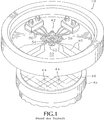
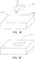
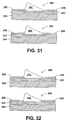
Der Meßfühler
Wenn, wie in
Ein Merkmal des Membranmeßfühleraufbaus
Der Membranaufbau ist durch eine dazwischenliegende Elastomerschicht
Wenn bei dem oben beschriebenen Aufbau, wie in
Da die Elastomerschicht
Es sei bei diesem Beispiel angemerkt, daß die Kippbewegung eines jeden Kontakts lokal geregelt ist, und daß die längeren Kontakte insbesondere in der Lage sind, unabhängig von den kürzeren Kontakten zu verkippen, so daß der kürzere Kontakt nicht seitlich verschoben wird, bevor er nicht tatsächlich mit seiner Kontaktfläche in Berührung gekommen ist.It should be noted in this example that the tilting movement of each contact is locally controlled, and that the longer contacts in particular are able to tilt independently of the shorter contacts, so that the shorter contact is not displaced laterally before it actually has come into contact with its contact surface.
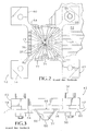
Mit Bezugnahme auf
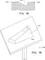
Jedoch führt die zuvor erläuterte Aufbautechnik unglücklicherweise zu einem Aufbau mit vielen unerwünschte Eigenschaften.Unfortunately, the previously discussed construction technique unfortunately results in a design with many undesirable characteristics.
Erstens führen die verschiedenen Arme
Zweitens ist die Fähigkeit, die Abstände (Schrittweite) zwischen den Vorrichtungen zu verringern, aufgrund des ”Pilzwucherungs”-Effekts des Galvanisierungsverfahrens an den Kanten des Polyimids
Drittens ist es schwierig, eine zweite Metalllage direkt auf eine ersten Metalllage aufzugalvanisieren, wie z. B. Kontaktierungsbereiche
Viertens besteht bei Anbringen einer Photoresistlage über einer nicht gleichförmigen Oberfläche die Gefahr, daß diese nicht vollständig deckend aufgetragen wird, was zu einer nicht gleichmäßigen Dicke des Photoresistmaterials als solchem führt. In
Fünftens sind getrennte Ausrichtungsprozesse notwendig, um die Arme
Was erwünscht ist, ist deshalb eine Technik zum Aufbau von Membranmessfühlern und eine Struktur derselben, welche zu einer einheitlicheren Größe der Vorrichtungen führen, sowie einem verringerten Abstand zwischen den Vorrichtungen, einer maximierten Querfestigkeit, erwünschten Geometrien und einer passenden Ausrichtung.What is desired, therefore, is a technique for constructing membrane probes and a structure thereof, which results in a more uniform size of the devices, as well as a reduced distance between the devices, maximized transverse strength, desired geometries, and proper alignment.
Zusammenfassung der ErfindungSummary of the invention
Die vorliegende Erfindung überwindet die Nachteile des Standes der Technik durch
- – Verfahren zum Herstellen eines Membranmessfühlers nach
den Ansprüchen 1, 30, 43, 78; - – Messfühleraufbauten
nach den Ansprüchen - – Verfahren zum Testen einer elektrischen Vorrichtung nach
den Ansprüchen 51 und 83; - – Verfahren zum Herstellen eines Messfühlers nach
den Ansprüchen 60, 63, 73.
- - Method for producing a membrane sensor according to
claims 1, 30, 43, 78; - - Sensor assemblies according to
claims - - Method for testing an electrical device according to
claims 51 and 83; - - Method for manufacturing a sensor according to
claims 60, 63, 73.
Die abhängigen Ansprüche betreffen vorteilhafte Ausführungsformen der erfindungsgemäßen Verfahren und Vorrichtungen.The dependent claims relate to advantageous embodiments of the method and apparatus according to the invention.
Die vorgenannten weiteren Ziele, Merkmale und Vorteile der Erfindung ergeben sich in genauerer Weise nach Betrachten der nachfolgenden detaillierten Beschreibung der Erfindung zusammen mit den beigefügten Figuren.The foregoing further objects, features and advantages of the invention will become more apparent upon consideration of the following detailed description of the invention taken in conjunction with the accompanying drawings.
Kurze FigurenbeschreibungShort description of the figures
Ausführliche Beschreibung der bevorzugten AusführungsformDetailed description of the preferred embodiment
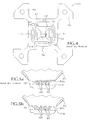
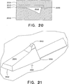
Die vorliegend angewandte Aufbautechnik für Membranmeßfühler beinhaltet als Ausgangspunkt ein flaches steifes Substrat, um weitere darauf aufzubringende Schichten zu stützen. Um die Schrittweite zu verringern und Vorrichtungen mit einer erhöhten Gleichmäßigkeit bereit zu stellen, sind immer noch komplexere und teuerere Bearbeitungsverfahren notwendig. Im direkten Gegensatz zu den herkömmlichen Techniken zum Aufbau von Schichten von unten nach oben auf einem Auflagesubstrat (Stützsubstrat) sind die Erfinder der vorliegenden Erfindung zu der Einsicht gelangt, daß durch Verwendung eines passenden Werkzeugs ein Substrat zielgerichtet so bearbeitet werden kann, daß die gewünschten Arme, Kontakthöcker und Kontaktierungsbereiche hergestellt werden können. Die verbleibenden Schichten werden dann von oben nach unten auf dem Arm hergestellt. Das Substrat selbst wird danach entfernt.The presently applied membrane sensor design technique incorporates as a starting point a flat rigid substrate to support additional layers to be deposited thereon. To reduce the pitch and provide devices with increased uniformity, more complex and expensive machining processes are still needed. In direct contrast to conventional bottom-up layer techniques on a support substrate, the inventors of the present invention have come to the conclusion that, by using a suitable tool, a substrate can be purposefully machined to provide the desired arms , Contact bumps and contacting areas can be made. The remaining layers are then made from top to bottom on the arm. The substrate itself is then removed.
Wie aus
Es ist teuer, Belichtungsmasken für die Polyimidschicht
Bevorzugterweise umfaßt die Maschine zum Anbringen von Vertiefungen eine genaue Z-Achsenbewegung, so daß die Tiefe einer jeden Vertiefung identisch ist oder im wesentlichen identisch ist. Ist eine ausreichend genaue Z-Achsenbewegung nicht möglich, so kann, wie in
In
Das zuvor erläuterte Verfahren des Aufbaus von oben nach unten stellt eine Vielzahl von Vorteilen gegenüber der herkömmlichen, von unten nach oben verlaufenden Bearbeitungstechnik zum Aufbau von Schichten auf einem Stützsubstrat bereit. Diese Vorteile ermöglichen es auch, Vorrichtungen mit verbesserten Eigenschaften aufzubauen.The above-described top-down construction method provides a variety of advantages over the conventional bottom-up machining technique for building layers on a backing substrate. These advantages also make it possible to build devices with improved properties.
Zuerst gibt es keine Beschränkungen bezüglich der Höhe der resultierenden Vorrichtungen, welche in der Vergangenheit durch das Bearbeiten mit Photoresist auferlegt worden sind. Die Möglichkeit, Vorrichtungen mit jeder passenden Höhe aufzubauen, beseitigt auch die Beschränkungen, welche bei den Versuchen aufgetreten sind, die hohen schmalen Öffnungen im Photoresist zu galvanisieren, was schwierig ist.First, there are no limitations on the height of the resulting devices which have been imposed in the past by photoresist processing. The ability to build devices of any suitable height also eliminates the limitations associated with attempts have been made to electroplate the high narrow openings in the photoresist, which is difficult.
Zweitens ist die Erhebung der Kontaktierungsbereiche
Drittens sind die Kontaktierungsbereiche der Vorrichtung stärker, da die Vorrichtung aus einem einzelnen homogenen Material aufgebaut ist während eines Abscheideprozesses, so daß keine Zwischenschichten erforderlich sind, wie dies früher bei Mehrfachbearbeitungsschritten erforderlich war. Dies erlaubt es, die Größe der Kontaktierungsbereiche bis zur Grenze der maximalen Stromdichte zu beschränken, welche während des Testens zulässig ist, und nicht auf die minimale Scherbelastbarkeit der Zwischenschicht.Third, the contacting areas of the device are stronger because the device is constructed of a single homogeneous material during a deposition process so that no intermediate layers are required, as previously required in multiple processing steps. This makes it possible to limit the size of the contacting areas to the limit of the maximum current density which is allowed during testing, and not to the minimum shear capacity of the intermediate layer.
Viertens sind die Formen der sich so ergebenden Vorrichtungen anpaßbar, um in effektiver Weise verschiedene Materialien zu testen. Die Form der Vorrichtung kann steile Seitenwandwinkel aufweisen, wie z. B. 85°, während sie gleichzeitig mechanische Festigkeit, Stabilität und Integrität aufweisen. Die steilen Seitenwände erlauben es, tiefere Vorrichtungen herzustellen, welche eine größere Dichte der Vorrichtungen erlauben, bis hin zu fortlaufend dichteren Packungen der Kontaktflächen auf der zu testenden Vorrichtung. Weiterhin ist der Winkel der Seitenwände nicht abhängig (d. h. unabhängig) vom Kristallgefüge des Substrats.Fourth, the shapes of the resulting devices are adaptable to effectively test different materials. The shape of the device may have steep side wall angles, such as. B. 85 °, while they have mechanical strength, stability and integrity. The steep side walls make it possible to produce deeper devices which allow greater device density, to progressively denser packages of contact surfaces on the device under test. Furthermore, the angle of the sidewalls is not dependent (i.e., independent) on the crystal structure of the substrate.
Fünftens ist die Form der Kontaktierungsbereiche genau bekannt und ist von Vorrichtung zu Vorrichtung gleichmäßig, was einen gleichmäßigen Kontakt mit den Kontaktflächen der zu testenden Vorrichtung ermöglicht.Fifth, the shape of the contacting areas is well known and uniform from device to device, allowing for even contact with the contact surfaces of the device under test.
Sechstens ist die Ausrichtung der verschiedenen Bereiche der resultierenden Vorrichtung exakt gleichmäßig von Vorrichtung zu Vorrichtung, da jede Vorrichtung unter Verwendung eines Verfahrens hergestellt worden ist, welches dasselbe Werkzeug verwendet. Mit einer exakten Ausrichtung der tieferen Bereiche einer jeden Vorrichtung (Arm und Kontakthöcker) im Verhältnis zum Kontaktierungsbereich gibt es keine Notwendigkeit, zusätzlich Spielraum bereit zu stellen, um die Schwankungen im Verfahren abzufangen, welche Photoresist- sowie Galvanisierungsverfahren eigen sind. Weiterhin wird auch der ”Pilzwucherungs”-Effekt beim Galvanisieren unterbunden, welcher ebenfalls die erforderliche Größe der Vorrichtung verringert. Die Verringerung der Schwankungen der Ausrichtung und praktische Eliminierung von Unterschieden in den Vorrichtungen
Siebtens kann die Form der resultierenden Vorrichtungen genau angepaßt werden, um eine optimale mechanische Belastbarkeit zu ermöglichen. Um, wie im Beschreibungseinleitungsteil erläutert, die Abbürstfunktion bereit zu stellen, sollte die Vorrichtung einen Aufbau von Arm und Höcker aufweisen, welcher bei Berührung verkippt. Die Vorrichtung
Achtens werden ”Aufsicht”-Kameras verwendet, um ein Bild des unteren Bereichs des Membranmeßfühlers zu bekommen und die genaue Positionierung der Vorrichtungen
Neuntens führt das anfängliche Polieren der Oberfläche
Zehntens werden, wie in
Elftens ist die Oberflächenstruktur des Kontaktierungsbereichs
Dreizehntens ist die erfindungsgemäße Technik zum Strukturaufbau relativ schnell, um die Vorrichtungen aufzubauen, da eine reduzierte Anzahl von Bearbeitungsschritten vorliegt, was auch zu erheblichen Kosteneinsparungen führt.Thirteen, the structure-building technique of the invention is relatively fast to build the devices because there are a reduced number of processing steps, which also leads to significant cost savings.
Die vorstehend erläuterte Herstellungstechnik stellt auch verschiedene Vorteile bereit in Bezug auf die Gestalt der Vorrichtungen, die anderenfalls nur schwerlich, wenn nicht überhaupt nicht erreicht werden könnten.The manufacturing technique discussed above also provides several advantages in terms of the shape of the devices, which would otherwise be difficult, if not impossible, to achieve.
Erstens kann das Werkzeug jede gewünschte Form bereit stellen, wie z. B. einen einfachen Höcker, falls keine Bürstwirkung erwünscht ist.First, the tool can provide any desired shape, such. B. a simple hump, if no brushing action is desired.
Zweitens stellen die geneigten Stützseiten der zu testenden Vorrichtung hin zu den Kontaktierungsbereichen
Drittens ist der Druck, welcher durch die Kontaktierungsbereiche der Vorrichtungen bei einem durch den Meßfühlerkopf vorgegebenen Druck ausgeübt wird, veränderbar, und zwar durch Ändern des Zentrums der Drehbewegung der Vorrichtung. Der Drehpunkt der Vorrichtung kann durch Auswahl der Länge der Vorrichtung und der Position/Höhe des Kontaktierungsbereichs relativ hierzu ausgewählt werden. Dementsprechend können die Drücke wie erwünscht ausgewählt werden, um zu den Eigenschaften der verschiedenen Kontaktflächen zu passen. Third, the pressure exerted by the contacting portions of the devices at a pressure set by the probe head is changeable by changing the center of rotational movement of the device. The fulcrum of the device can be selected by selecting the length of the device and the position / height of the contacting region relative thereto. Accordingly, the pressures may be selected as desired to suit the properties of the various contact surfaces.
Viertens ist in
Fünftens erlaubt es die Fähigkeit des Herstellens von Kontaktierungsbereichen, welche sich oberhalb der unteren Oberfläche der Vorrichtungen erheben, während gleichzeitig eine Gleichförmigkeit in der Höhe der Vorrichtungen und ihrer strukturellen Festigkeit beibehalten wird, daß die Vorrichtung eine Bürstwirkung zeigt, während die untere Oberfläche der Vorrichtung nur eine geringe Bewegung benötigt. Die geringe Bewegung der unteren Oberfläche der Vorrichtung, um während des Testens einen guten elektrischen Kontakt herzustellen, verringert die Spannung auf die Schichten unterhalb der unteren Oberfläche der Vorrichtung. Dementsprechend wird die Wahrscheinlichkeit des Reißens der Polyimidschichten und der Leiterbahnen verringert.Fifth, the ability to make contact areas which rise above the lower surface of the devices while maintaining uniformity in the height of the devices and their structural strength allows the device to exhibit a brushing action while the lower surface of the device only a little movement needed. The slight movement of the lower surface of the device to make good electrical contact during testing reduces the stress on the layers below the lower surface of the device. Accordingly, the likelihood of cracking of the polyimide layers and the conductive lines is reduced.
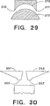
Beim Testen einer Oxidschicht auf Lothöckern oder Lotkugeln auf Wafern, welche mit einer ”flip-chip”-Packungstechnologie zu verwenden sind, so wie z. B. Lothöckern auf gedruckten Leiterplatten, ist die Oxidschicht, welche darauf ausgebildet ist, nur schwer effektiv zu durchdringen. Tritt ein herkömmlicher Kontaktierungsbereich eines Membranmeßfühlers mit einem Lothöcker in Kontakt, so besteht, wie in
Frühere Techniken zum Aufbau der Vorrichtungen führten zu Vorrichtungen, welche Kontaktierungsbereiche umfaßten, welche ziemlich groß waren und bei denen es schwierig war, ihre Ausrichtung sicher zu stellen.
Es sei angemerkt, daß abhängig von der verwendeten Technik, der gewünschten Verwendung und der erzielten Struktur, keine oder aber auch bis zu alle der zuvorgenannten und im folgenden beschriebenen Vorteile realisiert werden können in Vorrichtungen, welche gemäß der vorliegenden Erfindung hergestellt worden sind.It should be noted that, depending on the technique used, the desired use and the structure achieved, none or even all of the above-mentioned and below-described advantages can be realized in devices made according to the present invention.
Die Erfinder der vorliegenden Erfindung haben beobachtet, daß nach umfangreichem Gebrauch, wie z. B. 100 000 Prüfzyklen, die Leiterbahnen
Mit Berücksichtigung dieser Beschränkung der Prüfzykluszahl ist eine potentielle Technik, welche von den Erfindern der vorliegenden Erfindung vorgeschlagen wird, um die Anzahl der Zyklen zu erhöhen, die Maßnahme, daß die Leiterbahn
Die Erfinder der vorliegenden Erfindung, welche sich Sorgen gemacht haben wegen der zuvor genannten Beschränkungen, haben festgestellt, daß durch Herstellen dünnerer Leiterbahnen
Die Erfinder der vorliegenden Erfindung haben dann die Dreidimensionalität der Vorrichtung
Im Gegensatz zur Änderung der Dicke oder Breite der Leiter
Im Gegensatz zum Ändern der Dicke, der Breite oder des Aufbaus der Leiterbahn
Die Erfinder der vorliegenden Erfindung haben weiterhin festgestellt, daß die Steuerung der Verbiegung der Leiterbahn
Es versteht sich, daß auch andere Techniken als die hier beschriebenen verwendet werden können, und zwar individuell oder in Kombination mit anderen, wie erwünscht.It will be understood that techniques other than those described herein may be used, individually or in combination with others, as desired.
Die herkömmliche Lehrmeinung liegt nahe, daß die im wesentlichen rechteckförmige Form der Vorrichtung
Die Erfinder der vorliegenden Erfindung haben beobachtet, daß nach dem eine Vorrichtung
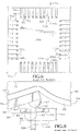
Die
Die Erfinder der vorliegenden Erfindung haben beobachtet, daß wenn das Werkzeug zum Anbringen von Vertiefungen verwendet wird, um nacheinander eine Serie von Vertiefungen herzustellen, wie in
Obwohl ein Werkzeug zur Anbringung von Vertiefungen mit vier Symmetrieachsen viele Vorteile aufweist, hat es eine etwas beschränkte Fähigkeit zum Anbringen von Schrittweiten. Um die Schrittweite der Vorrichtung (Dichte) zu vergrößern, kann ein Werkzeug zum Anbringen von Vertiefungen mit einer Zweiachs-Symmetrie verwendet werden, wie in
Während die in
Claims (100)
Applications Claiming Priority (2)
| Application Number | Priority Date | Filing Date | Title |
|---|---|---|---|
| US137759 | 1998-08-20 | ||
| US13775999P | 1999-06-04 | 1999-06-04 |
Publications (2)
| Publication Number | Publication Date |
|---|---|
| DE10023379A1 DE10023379A1 (en) | 2001-03-08 |
| DE10023379B4 true DE10023379B4 (en) | 2011-04-21 |
Family
ID=22478926
Family Applications (1)
| Application Number | Title | Priority Date | Filing Date |
|---|---|---|---|
| DE10023379A Expired - Fee Related DE10023379B4 (en) | 1999-06-04 | 2000-05-12 | Membrane probes and membrane probe assemblies, methods of making the same, and test methods used therewith |
Country Status (4)
| Country | Link |
|---|---|
| US (4) | US6578264B1 (en) |
| JP (1) | JP2001013168A (en) |
| KR (1) | KR100626166B1 (en) |
| DE (1) | DE10023379B4 (en) |
Families Citing this family (51)
| Publication number | Priority date | Publication date | Assignee | Title |
|---|---|---|---|---|
| US5914613A (en) | 1996-08-08 | 1999-06-22 | Cascade Microtech, Inc. | Membrane probing system with local contact scrub |
| US6256882B1 (en) | 1998-07-14 | 2001-07-10 | Cascade Microtech, Inc. | Membrane probing system |
| WO2000074110A2 (en) * | 1999-05-27 | 2000-12-07 | Nanonexus, Inc. | Integrated circuit wafer probe card assembly |
| US6578264B1 (en) * | 1999-06-04 | 2003-06-17 | Cascade Microtech, Inc. | Method for constructing a membrane probe using a depression |
| US6939474B2 (en) * | 1999-07-30 | 2005-09-06 | Formfactor, Inc. | Method for forming microelectronic spring structures on a substrate |
| US6914423B2 (en) | 2000-09-05 | 2005-07-05 | Cascade Microtech, Inc. | Probe station |
| US6965226B2 (en) | 2000-09-05 | 2005-11-15 | Cascade Microtech, Inc. | Chuck for holding a device under test |
| DE20114544U1 (en) | 2000-12-04 | 2002-02-21 | Cascade Microtech Inc | wafer probe |
| WO2003052435A1 (en) | 2001-08-21 | 2003-06-26 | Cascade Microtech, Inc. | Membrane probing system |
| JP2003215161A (en) * | 2002-01-22 | 2003-07-30 | Tokyo Electron Ltd | Probe, method of manufacturing probe, method and device for attaching probe, and probe card |
| KR100474420B1 (en) * | 2002-11-22 | 2005-03-10 | 주식회사 파이컴 | Probe sheet for testing flat pannel display, method thereby, probe assembly having it |
| KR100443999B1 (en) * | 2003-02-28 | 2004-08-21 | 주식회사 파이컴 | Interconnector for Printed Circuit Board, method thereby and interconnector assembly having it |
| US7492172B2 (en) | 2003-05-23 | 2009-02-17 | Cascade Microtech, Inc. | Chuck for holding a device under test |
| US7057404B2 (en) | 2003-05-23 | 2006-06-06 | Sharp Laboratories Of America, Inc. | Shielded probe for testing a device under test |
| US6853205B1 (en) * | 2003-07-17 | 2005-02-08 | Chipmos Technologies (Bermuda) Ltd. | Probe card assembly |
| US7250626B2 (en) | 2003-10-22 | 2007-07-31 | Cascade Microtech, Inc. | Probe testing structure |
| US7187188B2 (en) | 2003-12-24 | 2007-03-06 | Cascade Microtech, Inc. | Chuck with integrated wafer support |
| JP2007517231A (en) | 2003-12-24 | 2007-06-28 | カスケード マイクロテック インコーポレイテッド | Active wafer probe |
| US10641792B2 (en) | 2003-12-31 | 2020-05-05 | University Of Southern California | Multi-layer, multi-material micro-scale and millimeter-scale devices with enhanced electrical and/or mechanical properties |
| CA2569067C (en) * | 2004-06-01 | 2013-04-02 | James H. Adair | Unagglomerated core/shell nanocomposite particles |
| DE202005021435U1 (en) | 2004-09-13 | 2008-02-28 | Cascade Microtech, Inc., Beaverton | Double-sided test setups |
| US7535247B2 (en) | 2005-01-31 | 2009-05-19 | Cascade Microtech, Inc. | Interface for testing semiconductors |
| US7656172B2 (en) | 2005-01-31 | 2010-02-02 | Cascade Microtech, Inc. | System for testing semiconductors |
| US7245135B2 (en) * | 2005-08-01 | 2007-07-17 | Touchdown Technologies, Inc. | Post and tip design for a probe contact |
| JP4384724B2 (en) * | 2005-09-26 | 2009-12-16 | 日本電子材料株式会社 | Probe card manufacturing method |
| US7437813B2 (en) * | 2006-02-08 | 2008-10-21 | Sv Probe Pte Ltd. | Probe repair methods |
| US7723999B2 (en) | 2006-06-12 | 2010-05-25 | Cascade Microtech, Inc. | Calibration structures for differential signal probing |
| US7403028B2 (en) | 2006-06-12 | 2008-07-22 | Cascade Microtech, Inc. | Test structure and probe for differential signals |
| US7764072B2 (en) | 2006-06-12 | 2010-07-27 | Cascade Microtech, Inc. | Differential signal probing system |
| DE102006035644A1 (en) * | 2006-07-31 | 2008-02-14 | Advanced Micro Devices, Inc., Sunnyvale | A method of reducing contamination by providing a polymeric protective layer to be removed during processing of microstructures |
| KR100823310B1 (en) * | 2007-03-27 | 2008-04-18 | 세크론 주식회사 | Method for manufacturing probe card and probe card manufactured thereby |
| KR100908810B1 (en) * | 2007-06-11 | 2009-07-21 | 주식회사 제이엠엘 | Method for manufacturing micro tips and needles and vertical probes for probe cards |
| US7876114B2 (en) | 2007-08-08 | 2011-01-25 | Cascade Microtech, Inc. | Differential waveguide probe |
| KR101004911B1 (en) * | 2008-08-12 | 2010-12-28 | 삼성전기주식회사 | Fabrication method of micro electro-mechanical component |
| US7888957B2 (en) | 2008-10-06 | 2011-02-15 | Cascade Microtech, Inc. | Probing apparatus with impedance optimized interface |
| US8410806B2 (en) | 2008-11-21 | 2013-04-02 | Cascade Microtech, Inc. | Replaceable coupon for a probing apparatus |
| US8319503B2 (en) | 2008-11-24 | 2012-11-27 | Cascade Microtech, Inc. | Test apparatus for measuring a characteristic of a device under test |
| KR101022912B1 (en) * | 2008-11-28 | 2011-03-17 | 삼성전기주식회사 | A printed circuit board comprising a metal bump and a method of manufacturing the same |
| US8525168B2 (en) * | 2011-07-11 | 2013-09-03 | International Business Machines Corporation | Integrated circuit (IC) test probe |
| US9435855B2 (en) | 2013-11-19 | 2016-09-06 | Teradyne, Inc. | Interconnect for transmitting signals between a device and a tester |
| US9070586B1 (en) * | 2014-02-22 | 2015-06-30 | International Business Machines Corporation | Method of forming surface protrusions on an article and the article with the protrusions attached |
| US9594114B2 (en) | 2014-06-26 | 2017-03-14 | Teradyne, Inc. | Structure for transmitting signals in an application space between a device under test and test electronics |
| US9977052B2 (en) | 2016-10-04 | 2018-05-22 | Teradyne, Inc. | Test fixture |
| US10677815B2 (en) | 2018-06-08 | 2020-06-09 | Teradyne, Inc. | Test system having distributed resources |
| US11262383B1 (en) | 2018-09-26 | 2022-03-01 | Microfabrica Inc. | Probes having improved mechanical and/or electrical properties for making contact between electronic circuit elements and methods for making |
| US11363746B2 (en) | 2019-09-06 | 2022-06-14 | Teradyne, Inc. | EMI shielding for a signal trace |
| US11761982B1 (en) | 2019-12-31 | 2023-09-19 | Microfabrica Inc. | Probes with planar unbiased spring elements for electronic component contact and methods for making such probes |
| US11867721B1 (en) | 2019-12-31 | 2024-01-09 | Microfabrica Inc. | Probes with multiple springs, methods for making, and methods for using |
| US11774467B1 (en) | 2020-09-01 | 2023-10-03 | Microfabrica Inc. | Method of in situ modulation of structural material properties and/or template shape |
| US11862901B2 (en) | 2020-12-15 | 2024-01-02 | Teradyne, Inc. | Interposer |
| KR102309675B1 (en) | 2021-07-30 | 2021-10-07 | 김재길 | Probe card in film type |
Citations (22)
| Publication number | Priority date | Publication date | Assignee | Title |
|---|---|---|---|---|
| US3596228A (en) * | 1969-05-29 | 1971-07-27 | Ibm | Fluid actuated contactor |
| US4636772A (en) * | 1985-01-17 | 1987-01-13 | Riken Denshi Co. Ltd. | Multiple function type D/A converter |
| US4649339A (en) * | 1984-04-25 | 1987-03-10 | Honeywell Inc. | Integrated circuit interface |
| US4675638A (en) * | 1985-02-01 | 1987-06-23 | Dr. Ing. H.C.F. Porsche Aktiengesellschaft | Ferromagnetic multiple shell core for electric coils |
| EP0230348A2 (en) * | 1986-01-07 | 1987-07-29 | Hewlett-Packard Company | Test probe |
| EP0259163A2 (en) * | 1986-09-05 | 1988-03-09 | Tektronix, Inc. | Semiconductor wafer probe |
| US4793814A (en) * | 1986-07-21 | 1988-12-27 | Rogers Corporation | Electrical circuit board interconnect |
| EP0304868A2 (en) * | 1987-08-28 | 1989-03-01 | Tektronix Inc. | Multiple lead probe for integrated circuits in wafer form |
| US4918383A (en) * | 1987-01-20 | 1990-04-17 | Huff Richard E | Membrane probe with automatic contact scrub action |
| DE4012839A1 (en) * | 1989-04-26 | 1990-10-31 | Atg Electronic Gmbh | Test arrangement for electrical or electronic test objects - has contact needles connected to semiconducting plate via conducting blocks for close contact positioning |
| US4975638A (en) * | 1989-12-18 | 1990-12-04 | Wentworth Laboratories | Test probe assembly for testing integrated circuit devices |
| US4980637A (en) * | 1988-03-01 | 1990-12-25 | Hewlett-Packard Company | Force delivery system for improved precision membrane probe |
| US5059989A (en) * | 1990-05-16 | 1991-10-22 | Lexmark International, Inc. | Thermal edge jet drop-on-demand ink jet print head |
| US5134365A (en) * | 1989-07-11 | 1992-07-28 | Nihon Denshizairyo Kabushiki Kaisha | Probe card in which contact pressure and relative position of each probe end are correctly maintained |
| US5172050A (en) * | 1991-02-15 | 1992-12-15 | Motorola, Inc. | Micromachined semiconductor probe card |
| DE4223658A1 (en) * | 1991-07-18 | 1993-01-21 | Gold Star Electronics | Test appts. for semiconductor chips with relatively many connectors - uses tape automated bonding band with adhesive surface for connecting lines to test card and dendritically grown metal test points |
| US5355079A (en) * | 1993-01-07 | 1994-10-11 | Wentworth Laboratories, Inc. | Probe assembly for testing integrated circuit devices |
| US5389885A (en) * | 1992-01-27 | 1995-02-14 | Everett Charles Technologies, Inc. | Expandable diaphragm test modules and connectors |
| US5395253A (en) * | 1993-04-29 | 1995-03-07 | Hughes Aircraft Company | Membrane connector with stretch induced micro scrub |
| US5521518A (en) * | 1990-09-20 | 1996-05-28 | Higgins; H. Dan | Probe card apparatus |
| WO1998007040A1 (en) * | 1996-08-08 | 1998-02-19 | Cascade Microtech, Inc. | Membrane probing system with local contact scrub |
| US5869974A (en) * | 1996-04-01 | 1999-02-09 | Micron Technology, Inc. | Micromachined probe card having compliant contact members for testing semiconductor wafers |
Family Cites Families (283)
| Publication number | Priority date | Publication date | Assignee | Title |
|---|---|---|---|---|
| US1337866A (en) | 1917-09-27 | 1920-04-20 | Griffiths Ethel Grace | System for protecting electric cables |
| US2142625A (en) | 1932-07-06 | 1939-01-03 | Hollandsche Draad En Kabelfab | High tension cable |
| US2376101A (en) | 1942-04-01 | 1945-05-15 | Ferris Instr Corp | Electrical energy transmission |
| US2389668A (en) | 1943-03-04 | 1945-11-27 | Barnes Drill Co | Indexing mechanism for machine tables |
| US3193712A (en) | 1962-03-21 | 1965-07-06 | Clarence A Harris | High voltage cable |
| US3230299A (en) | 1962-07-18 | 1966-01-18 | Gen Cable Corp | Electrical cable with chemically bonded rubber layers |
| US3176091A (en) | 1962-11-07 | 1965-03-30 | Helmer C Hanson | Controlled multiple switching unit |
| US3401126A (en) | 1965-06-18 | 1968-09-10 | Ibm | Method of rendering noble metal conductive composition non-wettable by solder |
| US3429040A (en) | 1965-06-18 | 1969-02-25 | Ibm | Method of joining a component to a substrate |
| US3445770A (en) * | 1965-12-27 | 1969-05-20 | Philco Ford Corp | Microelectronic test probe with defect marker access |
| US3442831A (en) | 1966-04-21 | 1969-05-06 | Borden Co | Vinyl chloride polymerization process and latex |
| US3484679A (en) | 1966-10-03 | 1969-12-16 | North American Rockwell | Electrical apparatus for changing the effective capacitance of a cable |
| US3441315A (en) | 1967-07-07 | 1969-04-29 | Artnell Co | Seat and method for manufacturing the same |
| US3609539A (en) | 1968-09-28 | 1971-09-28 | Ibm | Self-aligning kelvin probe |
| US3595228A (en) | 1968-11-27 | 1971-07-27 | Robert C Simon | Flow line break alarm device |
| US3541222A (en) | 1969-01-13 | 1970-11-17 | Bunker Ramo | Connector screen for interconnecting adjacent surfaces of laminar circuits and method of making |
| NL7003475A (en) | 1969-03-28 | 1970-09-30 | ||
| US3654585A (en) | 1970-03-11 | 1972-04-04 | Brooks Research And Mfg Inc | Coordinate conversion for the testing of printed circuit boards |
| US3740900A (en) | 1970-07-01 | 1973-06-26 | Signetics Corp | Vacuum chuck assembly for semiconductor manufacture |
| US3700998A (en) | 1970-08-20 | 1972-10-24 | Computer Test Corp | Sample and hold circuit with switching isolation |
| US3714572A (en) | 1970-08-21 | 1973-01-30 | Rca Corp | Alignment and test fixture apparatus |
| US3680037A (en) | 1970-11-05 | 1972-07-25 | Tech Wire Prod Inc | Electrical interconnector |
| US3710251A (en) | 1971-04-07 | 1973-01-09 | Collins Radio Co | Microelectric heat exchanger pedestal |
| GB1387587A (en) | 1971-07-22 | 1975-03-19 | Plessey Co Ltd | Electrical interconnectors and connector assemblies |
| US3829076A (en) | 1972-06-08 | 1974-08-13 | H Sofy | Dial index machine |
| US3858212A (en) | 1972-08-29 | 1974-12-31 | L Tompkins | Multi-purpose information gathering and distribution system |
| US3952156A (en) | 1972-09-07 | 1976-04-20 | Xerox Corporation | Signal processing system |
| CA970849A (en) | 1972-09-18 | 1975-07-08 | Malcolm P. Macmartin | Low leakage isolating transformer for electromedical apparatus |
| US3806801A (en) | 1972-12-26 | 1974-04-23 | Ibm | Probe contactor having buckling beam probes |
| US3839672A (en) | 1973-02-05 | 1974-10-01 | Belden Corp | Method and apparatus for measuring the effectiveness of the shield in a coaxial cable |
| US3849728A (en) | 1973-08-21 | 1974-11-19 | Wentworth Labor Inc | Fixed point probe card and an assembly and repair fixture therefor |
| US3936743A (en) | 1974-03-05 | 1976-02-03 | Electroglas, Inc. | High speed precision chuck assembly |
| US3971610A (en) | 1974-05-10 | 1976-07-27 | Technical Wire Products, Inc. | Conductive elastomeric contacts and connectors |
| US3976959A (en) | 1974-07-22 | 1976-08-24 | Gaspari Russell A | Planar balun |
| US3970934A (en) | 1974-08-12 | 1976-07-20 | Akin Aksu | Printed circuit board testing means |
| US4038599A (en) | 1974-12-30 | 1977-07-26 | International Business Machines Corporation | High density wafer contacting and test system |
| US4038894A (en) | 1975-07-18 | 1977-08-02 | Springfield Tool And Die, Inc. | Piercing apparatus |
| SE407115B (en) | 1975-10-06 | 1979-03-12 | Kabi Ab | PROCEDURES AND METAL ELECTRODES FOR THE STUDY OF ENZYMATIC AND OTHER BIOCHEMICAL REACTIONS |
| US3992073A (en) | 1975-11-24 | 1976-11-16 | Technical Wire Products, Inc. | Multi-conductor probe |
| US4049252A (en) | 1976-02-04 | 1977-09-20 | Bell Theodore F | Index table |
| US4008900A (en) | 1976-03-15 | 1977-02-22 | John Freedom | Indexing chuck |
| US4099120A (en) | 1976-04-19 | 1978-07-04 | Akin Aksu | Probe head for testing printed circuit boards |
| US4027935A (en) | 1976-06-21 | 1977-06-07 | International Business Machines Corporation | Contact for an electrical contactor assembly |
| US4115735A (en) | 1976-10-14 | 1978-09-19 | Faultfinders, Inc. | Test fixture employing plural platens for advancing some or all of the probes of the test fixture |
| US4093988A (en) | 1976-11-08 | 1978-06-06 | General Electric Company | High speed frequency response measurement |
| US4312117A (en) | 1977-09-01 | 1982-01-26 | Raytheon Company | Integrated test and assembly device |
| US4184729A (en) | 1977-10-13 | 1980-01-22 | Bunker Ramo Corporation | Flexible connector cable |
| US4135131A (en) | 1977-10-14 | 1979-01-16 | The United States Of America As Represented By The Secretary Of The Army | Microwave time delay spectroscopic methods and apparatus for remote interrogation of biological targets |
| DE2849119A1 (en) | 1978-11-13 | 1980-05-14 | Siemens Ag | METHOD AND CIRCUIT FOR DAMPING MEASUREMENT, ESPECIALLY FOR DETERMINING THE DAMPING AND / OR GROUP DISTANCE DISTORTION OF A MEASURED OBJECT |
| US4383217A (en) | 1979-01-02 | 1983-05-10 | Shiell Thomas J | Collinear four-point probe head and mount for resistivity measurements |
| US4287473A (en) | 1979-05-25 | 1981-09-01 | The United States Of America As Represented By The United States Department Of Energy | Nondestructive method for detecting defects in photodetector and solar cell devices |
| FI58719C (en) | 1979-06-01 | 1981-04-10 | Instrumentarium Oy | DIAGNOSTISERINGSANORDNING FOER BROESTKANCER |
| US4277741A (en) | 1979-06-25 | 1981-07-07 | General Motors Corporation | Microwave acoustic spectrometer |
| US4327180A (en) | 1979-09-14 | 1982-04-27 | Board Of Governors, Wayne State Univ. | Method and apparatus for electromagnetic radiation of biological material |
| US4284033A (en) | 1979-10-31 | 1981-08-18 | Rca Corporation | Means to orbit and rotate target wafers supported on planet member |
| US4330783A (en) | 1979-11-23 | 1982-05-18 | Toia Michael J | Coaxially fed dipole antenna |
| US4284682A (en) | 1980-04-30 | 1981-08-18 | Nasa | Heat sealable, flame and abrasion resistant coated fabric |
| US4357575A (en) | 1980-06-17 | 1982-11-02 | Dit-Mco International Corporation | Apparatus for use in testing printed circuit process boards having means for positioning such boards in proper juxtaposition with electrical contacting assemblies |
| US4552033A (en) | 1980-07-08 | 1985-11-12 | Gebr. Marzhauser Wetzlar oHG | Drive system for a microscope stage or the like |
| US4376920A (en) | 1981-04-01 | 1983-03-15 | Smith Kenneth L | Shielded radio frequency transmission cable |
| US4425395A (en) | 1981-04-30 | 1984-01-10 | Fujikura Rubber Works, Ltd. | Base fabrics for polyurethane-coated fabrics, polyurethane-coated fabrics and processes for their production |
| US4401945A (en) | 1981-04-30 | 1983-08-30 | The Valeron Corporation | Apparatus for detecting the position of a probe relative to a workpiece |
| US4453142A (en) | 1981-11-02 | 1984-06-05 | Motorola Inc. | Microstrip to waveguide transition |
| DE3202461C1 (en) | 1982-01-27 | 1983-06-09 | Fa. Carl Zeiss, 7920 Heidenheim | Attachment of microscope objectives |
| US4468629A (en) | 1982-05-27 | 1984-08-28 | Trw Inc. | NPN Operational amplifier |
| US4528504A (en) | 1982-05-27 | 1985-07-09 | Harris Corporation | Pulsed linear integrated circuit tester |
| US4705447A (en) | 1983-08-11 | 1987-11-10 | Intest Corporation | Electronic test head positioner for test systems |
| US4487996A (en) | 1982-12-02 | 1984-12-11 | Electric Power Research Institute, Inc. | Shielded electrical cable |
| US4581679A (en) | 1983-05-31 | 1986-04-08 | Trw Inc. | Multi-element circuit construction |
| JPS59226167A (en) | 1983-06-04 | 1984-12-19 | Dainippon Screen Mfg Co Ltd | Surface treating device for circuit board |
| FR2547945B1 (en) | 1983-06-21 | 1986-05-02 | Raffinage Cie Francaise | NEW STRUCTURE OF ELECTRIC CABLE AND ITS APPLICATIONS |
| US4588950A (en) | 1983-11-15 | 1986-05-13 | Data Probe Corporation | Test system for VLSI digital circuit and method of testing |
| JPS60136006U (en) | 1984-02-20 | 1985-09-10 | 株式会社 潤工社 | flat cable |
| US4646005A (en) | 1984-03-16 | 1987-02-24 | Motorola, Inc. | Signal probe |
| US4697143A (en) | 1984-04-30 | 1987-09-29 | Cascade Microtech, Inc. | Wafer probe |
| JPS60235304A (en) | 1984-05-08 | 1985-11-22 | 株式会社フジクラ | Dc power cable |
| US4636722A (en) | 1984-05-21 | 1987-01-13 | Probe-Rite, Inc. | High density probe-head with isolated and shielded transmission lines |
| US4515133A (en) | 1984-05-31 | 1985-05-07 | Frank Roman | Fuel economizing device |
| US4837507A (en) | 1984-06-08 | 1989-06-06 | American Telephone And Telegraph Company At&T Technologies, Inc. | High frequency in-circuit test fixture |
| DK291184D0 (en) | 1984-06-13 | 1984-06-13 | Boeegh Petersen Allan | METHOD AND DEVICE FOR TESTING CIRCUIT PLATES |
| DE3428087A1 (en) | 1984-07-30 | 1986-01-30 | Kraftwerk Union AG, 4330 Mülheim | CONCENTRIC THREE-WIRE CABLE |
| US4593243A (en) | 1984-08-29 | 1986-06-03 | Magnavox Government And Industrial Electronics Company | Coplanar and stripline probe card apparatus |
| NL8403755A (en) * | 1984-12-11 | 1986-07-01 | Philips Nv | METHOD FOR MANUFACTURING A MULTI-LAYER PRINTED WIRING WITH SEW-THROUGH TRACKS IN DIFFERENT LAYERS AND MULTI-LAYER PRINTED WIRES MADE BY THE METHOD |
| US4713347A (en) | 1985-01-14 | 1987-12-15 | Sensor Diagnostics, Inc. | Measurement of ligand/anti-ligand interactions using bulk conductance |
| US4651115A (en) | 1985-01-31 | 1987-03-17 | Rca Corporation | Waveguide-to-microstrip transition |
| US4744041A (en) | 1985-03-04 | 1988-05-10 | International Business Machines Corporation | Method for testing DC motors |
| US4691163A (en) | 1985-03-19 | 1987-09-01 | Elscint Ltd. | Dual frequency surface probes |
| US4755746A (en) | 1985-04-24 | 1988-07-05 | Prometrix Corporation | Apparatus and methods for semiconductor wafer testing |
| US4684883A (en) | 1985-05-13 | 1987-08-04 | American Telephone And Telegraph Company, At&T Bell Laboratories | Method of manufacturing high-quality semiconductor light-emitting devices |
| FR2585513B1 (en) | 1985-07-23 | 1987-10-09 | Thomson Csf | COUPLING DEVICE BETWEEN A METAL WAVEGUIDE, A DIELECTRIC WAVEGUIDE AND A SEMICONDUCTOR COMPONENT, AND MIXER USING THE SAME |
| US4746857A (en) | 1985-09-13 | 1988-05-24 | Danippon Screen Mfg. Co. Ltd. | Probing apparatus for measuring electrical characteristics of semiconductor device formed on wafer |
| US4749942A (en) | 1985-09-26 | 1988-06-07 | Tektronix, Inc. | Wafer probe head |
| JPH0326643Y2 (en) | 1985-09-30 | 1991-06-10 | ||
| US5829128A (en) * | 1993-11-16 | 1998-11-03 | Formfactor, Inc. | Method of mounting resilient contact structures to semiconductor devices |
| US5476211A (en) * | 1993-11-16 | 1995-12-19 | Form Factor, Inc. | Method of manufacturing electrical contacts, using a sacrificial member |
| US6043563A (en) * | 1997-05-06 | 2000-03-28 | Formfactor, Inc. | Electronic components with terminals and spring contact elements extending from areas which are remote from the terminals |
| US5917707A (en) * | 1993-11-16 | 1999-06-29 | Formfactor, Inc. | Flexible contact structure with an electrically conductive shell |
| US4727319A (en) | 1985-12-24 | 1988-02-23 | Hughes Aircraft Company | Apparatus for on-wafer testing of electrical circuits |
| EP0442543B1 (en) * | 1986-01-24 | 1997-11-19 | Fuji Photo Film Co., Ltd. | Device for loading sheet films |
| JP2609232B2 (en) * | 1986-09-04 | 1997-05-14 | 日本ヒューレット・パッカード株式会社 | Floating drive circuit |
| US4673839A (en) | 1986-09-08 | 1987-06-16 | Tektronix, Inc. | Piezoelectric pressure sensing apparatus for integrated circuit testing stations |
| US4904933A (en) | 1986-09-08 | 1990-02-27 | Tektronix, Inc. | Integrated circuit probe station |
| US4772846A (en) * | 1986-12-29 | 1988-09-20 | Hughes Aircraft Company | Wafer alignment and positioning apparatus for chip testing by voltage contrast electron microscopy |
| US4727637A (en) | 1987-01-20 | 1988-03-01 | The Boeing Company | Computer aided connector assembly method and apparatus |
| US4827211A (en) | 1987-01-30 | 1989-05-02 | Cascade Microtech, Inc. | Wafer probe |
| US4711563A (en) | 1987-02-11 | 1987-12-08 | Lass Bennett D | Portable collapsible darkroom |
| US4912399A (en) | 1987-06-09 | 1990-03-27 | Tektronix, Inc. | Multiple lead probe for integrated circuits in wafer form |
| US4894612A (en) * | 1987-08-13 | 1990-01-16 | Hypres, Incorporated | Soft probe for providing high speed on-wafer connections to a circuit |
| US4791363A (en) | 1987-09-28 | 1988-12-13 | Logan John K | Ceramic microstrip probe blade |
| JP2554669Y2 (en) | 1987-11-10 | 1997-11-17 | 博 寺町 | Rotary positioning device |
| US5021186A (en) | 1988-03-25 | 1991-06-04 | Nissan Chemical Industries, Ltd. | Chloroisocyanuric acid composition having storage stability |
| US4871964A (en) | 1988-04-12 | 1989-10-03 | G. G. B. Industries, Inc. | Integrated circuit probing apparatus |
| US5323035A (en) | 1992-10-13 | 1994-06-21 | Glenn Leedy | Interconnection structure for integrated circuits and method for making same |
| US5020219A (en) | 1988-05-16 | 1991-06-04 | Leedy Glenn J | Method of making a flexible tester surface for testing integrated circuits |
| US5003253A (en) | 1988-05-20 | 1991-03-26 | The Board Of Trustees Of The Leland Stanford Junior University | Millimeter-wave active probe system |
| US4983910A (en) * | 1988-05-20 | 1991-01-08 | Stanford University | Millimeter-wave active probe |
| US4987100A (en) | 1988-05-26 | 1991-01-22 | International Business Machines Corporation | Flexible carrier for an electronic device |
| US4991290A (en) | 1988-07-21 | 1991-02-12 | Microelectronics And Computer Technology | Flexible electrical interconnect and method of making |
| US4922192A (en) | 1988-09-06 | 1990-05-01 | Unisys Corporation | Elastic membrane probe |
| US5634267A (en) * | 1991-06-04 | 1997-06-03 | Micron Technology, Inc. | Method and apparatus for manufacturing known good semiconductor die |
| US4906920A (en) | 1988-10-11 | 1990-03-06 | Hewlett-Packard Company | Self-leveling membrane probe |
| US4998062A (en) * | 1988-10-25 | 1991-03-05 | Tokyo Electron Limited | Probe device having micro-strip line structure |
| US4849689A (en) | 1988-11-04 | 1989-07-18 | Cascade Microtech, Inc. | Microwave wafer probe having replaceable probe tip |
| US4916002A (en) | 1989-01-13 | 1990-04-10 | The Board Of Trustees Of The Leland Jr. University | Microcasting of microminiature tips |
| US5045781A (en) | 1989-06-08 | 1991-09-03 | Cascade Microtech, Inc. | High-frequency active probe having replaceable contact needles |
| JPH0369131A (en) * | 1989-08-08 | 1991-03-25 | Fujitsu Ltd | Probe for semiconductor integrated circuit test use; manufacture of semiconductor device including test process using same probe |
| US5145552A (en) | 1989-12-21 | 1992-09-08 | Canon Kabushiki Kaisha | Process for preparing electrical connecting member |
| JPH03245527A (en) | 1990-02-23 | 1991-11-01 | Rohm Co Ltd | Fine processing |
| US5069628A (en) | 1990-03-13 | 1991-12-03 | Hughes Aircraft Company | Flexible electrical cable connector with double sided dots |
| US5059898A (en) | 1990-08-09 | 1991-10-22 | Tektronix, Inc. | Wafer probe with transparent loading member |
| US5589781A (en) | 1990-09-20 | 1996-12-31 | Higgins; H. Dan | Die carrier apparatus |
| US5126286A (en) | 1990-10-05 | 1992-06-30 | Micron Technology, Inc. | Method of manufacturing edge connected semiconductor die |
| US5207585A (en) | 1990-10-31 | 1993-05-04 | International Business Machines Corporation | Thin interface pellicle for dense arrays of electrical interconnects |
| US5148103A (en) | 1990-10-31 | 1992-09-15 | Hughes Aircraft Company | Apparatus for testing integrated circuits |
| US5061192A (en) | 1990-12-17 | 1991-10-29 | International Business Machines Corporation | High density connector |
| US5136237A (en) | 1991-01-29 | 1992-08-04 | Tektronix, Inc. | Double insulated floating high voltage test probe |
| US5097101A (en) | 1991-02-05 | 1992-03-17 | Tektronix, Inc. | Method of forming a conductive contact bump on a flexible substrate and a flexible substrate |
| US5133119A (en) | 1991-02-28 | 1992-07-28 | Hewlett-Packard Company | Shearing stress interconnection apparatus and method |
| US5487999A (en) | 1991-06-04 | 1996-01-30 | Micron Technology, Inc. | Method for fabricating a penetration limited contact having a rough textured surface |
| US5225037A (en) | 1991-06-04 | 1993-07-06 | Texas Instruments Incorporated | Method for fabrication of probe card for testing of semiconductor devices |
| US5229782A (en) * | 1991-07-19 | 1993-07-20 | Conifer Corporation | Stacked dual dipole MMDS feed |
| US5321352A (en) | 1991-08-01 | 1994-06-14 | Tokyo Electron Yamanashi Limited | Probe apparatus and method of alignment for the same |
| US5177438A (en) | 1991-08-02 | 1993-01-05 | Motorola, Inc. | Low resistance probe for semiconductor |
| JPH07105420B2 (en) * | 1991-08-26 | 1995-11-13 | ヒューズ・エアクラフト・カンパニー | Electrical connection with molded contacts |
| US5180977A (en) | 1991-12-02 | 1993-01-19 | Hoya Corporation Usa | Membrane probe contact bump compliancy system |
| US5274336A (en) | 1992-01-14 | 1993-12-28 | Hewlett-Packard Company | Capacitively-coupled test probe |
| US5367165A (en) | 1992-01-17 | 1994-11-22 | Olympus Optical Co., Ltd. | Cantilever chip for scanning probe microscope |
| US5584120A (en) | 1992-02-14 | 1996-12-17 | Research Organization For Circuit Knowledge | Method of manufacturing printed circuits |
| US6380751B2 (en) * | 1992-06-11 | 2002-04-30 | Cascade Microtech, Inc. | Wafer probe station having environment control enclosure |
| US6295729B1 (en) * | 1992-10-19 | 2001-10-02 | International Business Machines Corporation | Angled flying lead wire bonding process |
| US5371654A (en) * | 1992-10-19 | 1994-12-06 | International Business Machines Corporation | Three dimensional high performance interconnection package |
| US5479108A (en) | 1992-11-25 | 1995-12-26 | David Cheng | Method and apparatus for handling wafers |
| US5326412A (en) | 1992-12-22 | 1994-07-05 | Hughes Aircraft Company | Method for electrodepositing corrosion barrier on isolated circuitry |
| JPH0792479B2 (en) | 1993-03-18 | 1995-10-09 | 東京エレクトロン株式会社 | Parallelism adjustment method for probe device |
| US5390412A (en) * | 1993-04-08 | 1995-02-21 | Gregoire; George D. | Method for making printed circuit boards |
| US6054651A (en) * | 1996-06-21 | 2000-04-25 | International Business Machines Corporation | Foamed elastomers for wafer probing applications and interposer connectors |
| US6722032B2 (en) * | 1995-11-27 | 2004-04-20 | International Business Machines Corporation | Method of forming a structure for electronic devices contact locations |
| US6528984B2 (en) * | 1996-09-13 | 2003-03-04 | Ibm Corporation | Integrated compliant probe for wafer level test and burn-in |
| JP3346838B2 (en) | 1993-06-29 | 2002-11-18 | 有限会社創造庵 | Rotary movement mechanism |
| US5412866A (en) | 1993-07-01 | 1995-05-09 | Hughes Aircraft Company | Method of making a cast elastomer/membrane test probe assembly |
| US5441690A (en) | 1993-07-06 | 1995-08-15 | International Business Machines Corporation | Process of making pinless connector |
| US5326428A (en) * | 1993-09-03 | 1994-07-05 | Micron Semiconductor, Inc. | Method for testing semiconductor circuitry for operability and method of forming apparatus for testing semiconductor circuitry for operability |
| JP2710544B2 (en) | 1993-09-30 | 1998-02-10 | インターナショナル・ビジネス・マシーンズ・コーポレイション | Probe structure, method of forming probe structure |
| US5878486A (en) * | 1993-11-16 | 1999-03-09 | Formfactor, Inc. | Method of burning-in semiconductor devices |
| US6525555B1 (en) * | 1993-11-16 | 2003-02-25 | Formfactor, Inc. | Wafer-level burn-in and test |
| US6836962B2 (en) * | 1993-11-16 | 2005-01-04 | Formfactor, Inc. | Method and apparatus for shaping spring elements |
| US5832601A (en) * | 1993-11-16 | 1998-11-10 | Form Factor, Inc. | Method of making temporary connections between electronic components |
| US6442831B1 (en) * | 1993-11-16 | 2002-09-03 | Formfactor, Inc. | Method for shaping spring elements |
| US6184053B1 (en) * | 1993-11-16 | 2001-02-06 | Formfactor, Inc. | Method of making microelectronic spring contact elements |
| US6029344A (en) * | 1993-11-16 | 2000-02-29 | Formfactor, Inc. | Composite interconnection element for microelectronic components, and method of making same |
| US5601740A (en) * | 1993-11-16 | 1997-02-11 | Formfactor, Inc. | Method and apparatus for wirebonding, for severing bond wires, and for forming balls on the ends of bond wires |
| US6727580B1 (en) * | 1993-11-16 | 2004-04-27 | Formfactor, Inc. | Microelectronic spring contact elements |
| US5974662A (en) | 1993-11-16 | 1999-11-02 | Formfactor, Inc. | Method of planarizing tips of probe elements of a probe card assembly |
| US6023103A (en) * | 1994-11-15 | 2000-02-08 | Formfactor, Inc. | Chip-scale carrier for semiconductor devices including mounted spring contacts |
| JPH07311206A (en) * | 1994-05-19 | 1995-11-28 | Canon Inc | Manufacture of micro-probe |
| US5506515A (en) * | 1994-07-20 | 1996-04-09 | Cascade Microtech, Inc. | High-frequency probe tip assembly |
| JPH10505162A (en) | 1994-09-09 | 1998-05-19 | マイクロモジュール・システムズ | Circuit membrane probe |
| EP0707214A3 (en) | 1994-10-14 | 1997-04-16 | Hughes Aircraft Co | Multiport membrane probe for full-wafer testing |
| WO1996013967A1 (en) | 1994-10-28 | 1996-05-09 | Micromodule Systems | Programmable high density electronic testing device |
| US6727579B1 (en) * | 1994-11-16 | 2004-04-27 | Formfactor, Inc. | Electrical contact structures formed by configuring a flexible wire to have a springable shape and overcoating the wire with at least one layer of a resilient conductive material, methods of mounting the contact structures to electronic components, and applications for employing the contact structures |
| US5720098A (en) | 1995-05-12 | 1998-02-24 | Probe Technology | Method for making a probe preserving a uniform stress distribution under deflection |
| US6033935A (en) * | 1997-06-30 | 2000-03-07 | Formfactor, Inc. | Sockets for "springed" semiconductor devices |
| US6042712A (en) * | 1995-05-26 | 2000-03-28 | Formfactor, Inc. | Apparatus for controlling plating over a face of a substrate |
| US6685817B1 (en) * | 1995-05-26 | 2004-02-03 | Formfactor, Inc. | Method and apparatus for controlling plating over a face of a substrate |
| US5742174A (en) * | 1995-11-03 | 1998-04-21 | Probe Technology | Membrane for holding a probe tip in proper location |
| JP3838381B2 (en) * | 1995-11-22 | 2006-10-25 | 株式会社アドバンテスト | Probe card |
| DE19605598C1 (en) | 1996-02-15 | 1996-10-31 | Singulus Technologies Gmbh | Substrate hold and release mechanism for vacuum chamber |
| US5726211A (en) * | 1996-03-21 | 1998-03-10 | International Business Machines Corporation | Process for making a foamed elastometric polymer |
| KR100471341B1 (en) * | 1996-05-23 | 2005-07-21 | 제네시스 테크놀로지 가부시키가이샤 | Contact Probe and Probe Device with It |
| US6050829A (en) * | 1996-08-28 | 2000-04-18 | Formfactor, Inc. | Making discrete power connections to a space transformer of a probe card assembly |
| US5869326A (en) * | 1996-09-09 | 1999-02-09 | Genetronics, Inc. | Electroporation employing user-configured pulsing scheme |
| US5896038A (en) | 1996-11-08 | 1999-04-20 | W. L. Gore & Associates, Inc. | Method of wafer level burn-in |
| JPH10142259A (en) * | 1996-11-14 | 1998-05-29 | Mitsubishi Materials Corp | Manufacture of contact probe, contact probe using same, and probe device provided with contact probe |
| US6690185B1 (en) * | 1997-01-15 | 2004-02-10 | Formfactor, Inc. | Large contactor with multiple, aligned contactor units |
| US6520778B1 (en) * | 1997-02-18 | 2003-02-18 | Formfactor, Inc. | Microelectronic contact structures, and methods of making same |
| US6215196B1 (en) * | 1997-06-30 | 2001-04-10 | Formfactor, Inc. | Electronic component with terminals and spring contact elements extending from areas which are remote from the terminals |
| JPH1194863A (en) * | 1997-09-12 | 1999-04-09 | Nikon Corp | Cantilever and its manufacture |
| US6059982A (en) | 1997-09-30 | 2000-05-09 | International Business Machines Corporation | Micro probe assembly and method of fabrication |
| US6166333A (en) * | 1998-01-14 | 2000-12-26 | Packard Hughes Interconnect Company | Bumps with plural under-bump dielectric layers |
| JP3862845B2 (en) * | 1998-02-05 | 2006-12-27 | セイコーインスツル株式会社 | Near-field optical probe |
| US6807734B2 (en) * | 1998-02-13 | 2004-10-26 | Formfactor, Inc. | Microelectronic contact structures, and methods of making same |
| JP3553791B2 (en) * | 1998-04-03 | 2004-08-11 | 株式会社ルネサステクノロジ | CONNECTION DEVICE AND ITS MANUFACTURING METHOD, INSPECTION DEVICE, AND SEMICONDUCTOR ELEMENT MANUFACTURING METHOD |
| US6720501B1 (en) * | 1998-04-14 | 2004-04-13 | Formfactor, Inc. | PC board having clustered blind vias |
| US6256882B1 (en) * | 1998-07-14 | 2001-07-10 | Cascade Microtech, Inc. | Membrane probing system |
| US6160412A (en) * | 1998-11-05 | 2000-12-12 | Wentworth Laboratories, Inc. | Impedance-matched interconnection device for connecting a vertical-pin integrated circuit probing device to integrated circuit test equipment |
| US6672875B1 (en) * | 1998-12-02 | 2004-01-06 | Formfactor, Inc. | Spring interconnect structures |
| US6404211B2 (en) * | 1999-02-11 | 2002-06-11 | International Business Machines Corporation | Metal buckling beam probe |
| US6206273B1 (en) * | 1999-02-17 | 2001-03-27 | International Business Machines Corporation | Structures and processes to create a desired probetip contact geometry on a wafer test probe |
| US6539531B2 (en) * | 1999-02-25 | 2003-03-25 | Formfactor, Inc. | Method of designing, fabricating, testing and interconnecting an IC to external circuit nodes |
| US6218910B1 (en) * | 1999-02-25 | 2001-04-17 | Formfactor, Inc. | High bandwidth passive integrated circuit tester probe card assembly |
| US6448865B1 (en) * | 1999-02-25 | 2002-09-10 | Formfactor, Inc. | Integrated circuit interconnect system |
| US6208225B1 (en) * | 1999-02-25 | 2001-03-27 | Formfactor, Inc. | Filter structures for integrated circuit interfaces |
| US6538538B2 (en) * | 1999-02-25 | 2003-03-25 | Formfactor, Inc. | High frequency printed circuit board via |
| US6499121B1 (en) * | 1999-03-01 | 2002-12-24 | Formfactor, Inc. | Distributed interface for parallel testing of multiple devices using a single tester channel |
| US6419500B1 (en) * | 1999-03-08 | 2002-07-16 | Kulicke & Soffa Investment, Inc. | Probe assembly having floatable buckling beam probes and apparatus for abrading the same |
| AU5171800A (en) * | 1999-05-27 | 2000-12-18 | Nanonexus, Inc. | Massively parallel interface for electronic circuit |
| US6578264B1 (en) * | 1999-06-04 | 2003-06-17 | Cascade Microtech, Inc. | Method for constructing a membrane probe using a depression |
| US7013221B1 (en) * | 1999-07-16 | 2006-03-14 | Rosetta Inpharmatics Llc | Iterative probe design and detailed expression profiling with flexible in-situ synthesis arrays |
| US6713374B2 (en) * | 1999-07-30 | 2004-03-30 | Formfactor, Inc. | Interconnect assemblies and methods |
| US7009415B2 (en) * | 1999-10-06 | 2006-03-07 | Tokyo Electron Limited | Probing method and probing apparatus |
| JP2001174482A (en) * | 1999-12-21 | 2001-06-29 | Toshiba Corp | Contact needle for evaluating electric characteristic, probe structure, probe card and manufacturing method of contact needle for evaluating electric characteristic |
| JP2001201516A (en) * | 2000-01-18 | 2001-07-27 | Micronics Japan Co Ltd | Manufacturing method and device of probe element and hollow forming device |
| US6339338B1 (en) * | 2000-01-18 | 2002-01-15 | Formfactor, Inc. | Apparatus for reducing power supply noise in an integrated circuit |
| US6509751B1 (en) * | 2000-03-17 | 2003-01-21 | Formfactor, Inc. | Planarizer for a semiconductor contactor |
| US6677744B1 (en) * | 2000-04-13 | 2004-01-13 | Formfactor, Inc. | System for measuring signal path resistance for an integrated circuit tester interconnect structure |
| US6441629B1 (en) * | 2000-05-31 | 2002-08-27 | Advantest Corp | Probe contact system having planarity adjustment mechanism |
| US6424164B1 (en) * | 2000-06-13 | 2002-07-23 | Kulicke & Soffa Investment, Inc. | Probe apparatus having removable beam probes |
| US6420887B1 (en) * | 2000-06-13 | 2002-07-16 | Kulicke & Soffa Investment, Inc. | Modulated space transformer for high density buckling beam probe and method for making the same |
| US6731128B2 (en) * | 2000-07-13 | 2004-05-04 | International Business Machines Corporation | TFI probe I/O wrap test method |
| US6970005B2 (en) * | 2000-08-24 | 2005-11-29 | Texas Instruments Incorporated | Multiple-chip probe and universal tester contact assemblage |
| GB0021975D0 (en) * | 2000-09-07 | 2000-10-25 | Optomed As | Filter optic probes |
| US7005842B2 (en) * | 2000-12-22 | 2006-02-28 | Tokyo Electron Limited | Probe cartridge assembly and multi-probe assembly |
| US6756797B2 (en) * | 2001-01-31 | 2004-06-29 | Wentworth Laboratories Inc. | Planarizing interposer for thermal compensation of a probe card |
| US7006046B2 (en) * | 2001-02-15 | 2006-02-28 | Integral Technologies, Inc. | Low cost electronic probe devices manufactured from conductive loaded resin-based materials |
| US6856150B2 (en) * | 2001-04-10 | 2005-02-15 | Formfactor, Inc. | Probe card with coplanar daughter card |
| US6882239B2 (en) * | 2001-05-08 | 2005-04-19 | Formfactor, Inc. | Electromagnetically coupled interconnect system |
| US6525552B2 (en) * | 2001-05-11 | 2003-02-25 | Kulicke And Soffa Investments, Inc. | Modular probe apparatus |
| JP2002343879A (en) * | 2001-05-15 | 2002-11-29 | Nec Corp | Semiconductor device and method of manufacturing the same |
| JP3979793B2 (en) * | 2001-05-29 | 2007-09-19 | 日立ソフトウエアエンジニアリング株式会社 | Probe design apparatus and probe design method |
| US6729019B2 (en) * | 2001-07-11 | 2004-05-04 | Formfactor, Inc. | Method of manufacturing a probe card |
| US6862727B2 (en) * | 2001-08-24 | 2005-03-01 | Formfactor, Inc. | Process and apparatus for adjusting traces |
| US6678876B2 (en) * | 2001-08-24 | 2004-01-13 | Formfactor, Inc. | Process and apparatus for finding paths through a routing space |
| US6549106B2 (en) * | 2001-09-06 | 2003-04-15 | Cascade Microtech, Inc. | Waveguide with adjustable backshort |
| US6714828B2 (en) * | 2001-09-17 | 2004-03-30 | Formfactor, Inc. | Method and system for designing a probe card |
| US6906540B2 (en) * | 2001-09-20 | 2005-06-14 | Wentworth Laboratories, Inc. | Method for chemically etching photo-defined micro electrical contacts |
| DE10294376D2 (en) * | 2001-09-24 | 2004-08-26 | Jpk Instruments Ag | Device and method for a scanning probe microscope |
| US6882546B2 (en) * | 2001-10-03 | 2005-04-19 | Formfactor, Inc. | Multiple die interconnect system |
| US7071714B2 (en) * | 2001-11-02 | 2006-07-04 | Formfactor, Inc. | Method and system for compensating for thermally induced motion of probe cards |
| JP3976733B2 (en) * | 2001-11-13 | 2007-09-19 | 株式会社アドバンテスト | Chromatic dispersion measurement system and method |
| US7020363B2 (en) * | 2001-12-28 | 2006-03-28 | Intel Corporation | Optical probe for wafer testing |
| US7015707B2 (en) * | 2002-03-20 | 2006-03-21 | Gabe Cherian | Micro probe |
| US6828767B2 (en) * | 2002-03-20 | 2004-12-07 | Santronics, Inc. | Hand-held voltage detection probe |
| US6806697B2 (en) * | 2002-04-05 | 2004-10-19 | Agilent Technologies, Inc. | Apparatus and method for canceling DC errors and noise generated by ground shield current in a probe |
| DE10220343B4 (en) * | 2002-05-07 | 2007-04-05 | Atg Test Systems Gmbh & Co. Kg Reicholzheim | Apparatus and method for testing printed circuit boards and probes |
| US6881072B2 (en) * | 2002-10-01 | 2005-04-19 | International Business Machines Corporation | Membrane probe with anchored elements |
| US7026832B2 (en) * | 2002-10-28 | 2006-04-11 | Dainippon Screen Mfg. Co., Ltd. | Probe mark reading device and probe mark reading method |
| US6864694B2 (en) * | 2002-10-31 | 2005-03-08 | Agilent Technologies, Inc. | Voltage probe |
| US6727716B1 (en) * | 2002-12-16 | 2004-04-27 | Newport Fab, Llc | Probe card and probe needle for high frequency testing |
| JP2004199796A (en) * | 2002-12-19 | 2004-07-15 | Shinka Jitsugyo Kk | Method for connecting probe pin for measuring characteristics of thin-film magnetic head and method for measuring characteristics of thin-film magnetic head |
| US7132839B2 (en) * | 2002-12-31 | 2006-11-07 | Intel Corporation | Ultra-short low-force vertical probe test head and method |
| JP2004265942A (en) * | 2003-02-20 | 2004-09-24 | Okutekku:Kk | Method for detecting zero point of probe pin and probe |
| US7022976B1 (en) * | 2003-04-02 | 2006-04-04 | Advanced Micro Devices, Inc. | Dynamically adjustable probe tips |
| US7002133B2 (en) * | 2003-04-11 | 2006-02-21 | Hewlett-Packard Development Company, L.P. | Detecting one or more photons from their interactions with probe photons in a matter system |
| US7023225B2 (en) * | 2003-04-16 | 2006-04-04 | Lsi Logic Corporation | Wafer-mounted micro-probing platform |
| TWI220163B (en) * | 2003-04-24 | 2004-08-11 | Ind Tech Res Inst | Manufacturing method of high-conductivity nanometer thin-film probe card |
| KR100523139B1 (en) * | 2003-06-23 | 2005-10-20 | 주식회사 하이닉스반도체 | Semiconductor device for reducing the number of probing pad used during wafer testing and method for testing the same |
| US6956388B2 (en) * | 2003-06-24 | 2005-10-18 | Agilent Technologies, Inc. | Multiple two axis floating probe assembly using split probe block |
| US6870381B2 (en) * | 2003-06-27 | 2005-03-22 | Formfactor, Inc. | Insulative covering of probe tips |
| US7015708B2 (en) * | 2003-07-11 | 2006-03-21 | Gore Enterprise Holdings, Inc. | Method and apparatus for a high frequency, impedance controlled probing device with flexible ground contacts |
| US7015703B2 (en) * | 2003-08-12 | 2006-03-21 | Scientific Systems Research Limited | Radio frequency Langmuir probe |
| US7025628B2 (en) * | 2003-08-13 | 2006-04-11 | Agilent Technologies, Inc. | Electronic probe extender |
| JP3812559B2 (en) * | 2003-09-18 | 2006-08-23 | Tdk株式会社 | Eddy current probe |
| US7286013B2 (en) * | 2003-09-18 | 2007-10-23 | Avago Technologies Wireless Ip (Singapore) Pte Ltd | Coupled-inductance differential amplifier |
| US7034553B2 (en) * | 2003-12-05 | 2006-04-25 | Prodont, Inc. | Direct resistance measurement corrosion probe |
| US7009188B2 (en) * | 2004-05-04 | 2006-03-07 | Micron Technology, Inc. | Lift-out probe having an extension tip, methods of making and using, and analytical instruments employing same |
| US7015709B2 (en) * | 2004-05-12 | 2006-03-21 | Delphi Technologies, Inc. | Ultra-broadband differential voltage probes |
| US7023231B2 (en) * | 2004-05-14 | 2006-04-04 | Solid State Measurements, Inc. | Work function controlled probe for measuring properties of a semiconductor wafer and method of use thereof |
| US7019541B2 (en) * | 2004-05-14 | 2006-03-28 | Crown Products, Inc. | Electric conductivity water probe |
| US7015690B2 (en) * | 2004-05-27 | 2006-03-21 | General Electric Company | Omnidirectional eddy current probe and inspection system |
| TWI252925B (en) * | 2004-07-05 | 2006-04-11 | Yulim Hitech Inc | Probe card for testing a semiconductor device |
| JP4980903B2 (en) * | 2004-07-07 | 2012-07-18 | カスケード マイクロテック インコーポレイテッド | Probe head with membrane suspension probe |
| US7001785B1 (en) * | 2004-12-06 | 2006-02-21 | Veeco Instruments, Inc. | Capacitance probe for thin dielectric film characterization |
| US7005879B1 (en) * | 2005-03-01 | 2006-02-28 | International Business Machines Corporation | Device for probe card power bus noise reduction |
-
2000
- 2000-04-11 US US09/546,927 patent/US6578264B1/en not_active Expired - Lifetime
- 2000-05-12 DE DE10023379A patent/DE10023379B4/en not_active Expired - Fee Related
- 2000-06-03 KR KR1020000030592A patent/KR100626166B1/en active IP Right Grant
- 2000-06-05 JP JP2000167610A patent/JP2001013168A/en active Pending
-
2003
- 2003-04-16 US US10/418,510 patent/US7178236B2/en not_active Expired - Fee Related
-
2006
- 2006-12-01 US US11/607,156 patent/US7533462B2/en not_active Expired - Fee Related
-
2009
- 2009-02-18 US US12/378,650 patent/US20090178277A1/en not_active Abandoned
Patent Citations (22)
| Publication number | Priority date | Publication date | Assignee | Title |
|---|---|---|---|---|
| US3596228A (en) * | 1969-05-29 | 1971-07-27 | Ibm | Fluid actuated contactor |
| US4649339A (en) * | 1984-04-25 | 1987-03-10 | Honeywell Inc. | Integrated circuit interface |
| US4636772A (en) * | 1985-01-17 | 1987-01-13 | Riken Denshi Co. Ltd. | Multiple function type D/A converter |
| US4675638A (en) * | 1985-02-01 | 1987-06-23 | Dr. Ing. H.C.F. Porsche Aktiengesellschaft | Ferromagnetic multiple shell core for electric coils |
| EP0230348A2 (en) * | 1986-01-07 | 1987-07-29 | Hewlett-Packard Company | Test probe |
| US4793814A (en) * | 1986-07-21 | 1988-12-27 | Rogers Corporation | Electrical circuit board interconnect |
| EP0259163A2 (en) * | 1986-09-05 | 1988-03-09 | Tektronix, Inc. | Semiconductor wafer probe |
| US4918383A (en) * | 1987-01-20 | 1990-04-17 | Huff Richard E | Membrane probe with automatic contact scrub action |
| EP0304868A2 (en) * | 1987-08-28 | 1989-03-01 | Tektronix Inc. | Multiple lead probe for integrated circuits in wafer form |
| US4980637A (en) * | 1988-03-01 | 1990-12-25 | Hewlett-Packard Company | Force delivery system for improved precision membrane probe |
| DE4012839A1 (en) * | 1989-04-26 | 1990-10-31 | Atg Electronic Gmbh | Test arrangement for electrical or electronic test objects - has contact needles connected to semiconducting plate via conducting blocks for close contact positioning |
| US5134365A (en) * | 1989-07-11 | 1992-07-28 | Nihon Denshizairyo Kabushiki Kaisha | Probe card in which contact pressure and relative position of each probe end are correctly maintained |
| US4975638A (en) * | 1989-12-18 | 1990-12-04 | Wentworth Laboratories | Test probe assembly for testing integrated circuit devices |
| US5059989A (en) * | 1990-05-16 | 1991-10-22 | Lexmark International, Inc. | Thermal edge jet drop-on-demand ink jet print head |
| US5521518A (en) * | 1990-09-20 | 1996-05-28 | Higgins; H. Dan | Probe card apparatus |
| US5172050A (en) * | 1991-02-15 | 1992-12-15 | Motorola, Inc. | Micromachined semiconductor probe card |
| DE4223658A1 (en) * | 1991-07-18 | 1993-01-21 | Gold Star Electronics | Test appts. for semiconductor chips with relatively many connectors - uses tape automated bonding band with adhesive surface for connecting lines to test card and dendritically grown metal test points |
| US5389885A (en) * | 1992-01-27 | 1995-02-14 | Everett Charles Technologies, Inc. | Expandable diaphragm test modules and connectors |
| US5355079A (en) * | 1993-01-07 | 1994-10-11 | Wentworth Laboratories, Inc. | Probe assembly for testing integrated circuit devices |
| US5395253A (en) * | 1993-04-29 | 1995-03-07 | Hughes Aircraft Company | Membrane connector with stretch induced micro scrub |
| US5869974A (en) * | 1996-04-01 | 1999-02-09 | Micron Technology, Inc. | Micromachined probe card having compliant contact members for testing semiconductor wafers |
| WO1998007040A1 (en) * | 1996-08-08 | 1998-02-19 | Cascade Microtech, Inc. | Membrane probing system with local contact scrub |
Non-Patent Citations (1)
| Title |
|---|
| KIM,Yong-Dae, et.al.: Fabrication of a Silicon Micro-Probe for Vertical Probe Card Application. In: Jpn. J. Appl. Phys., Vol.37, 1998, S.7070-S.7073 * |
Also Published As
| Publication number | Publication date |
|---|---|
| US20090178277A1 (en) | 2009-07-16 |
| US20070074392A1 (en) | 2007-04-05 |
| KR20010029783A (en) | 2001-04-16 |
| JP2001013168A (en) | 2001-01-19 |
| KR100626166B1 (en) | 2006-09-20 |
| US7533462B2 (en) | 2009-05-19 |
| US20030192183A1 (en) | 2003-10-16 |
| US6578264B1 (en) | 2003-06-17 |
| DE10023379A1 (en) | 2001-03-08 |
| US7178236B2 (en) | 2007-02-20 |
Similar Documents
| Publication | Publication Date | Title |
|---|---|---|
| DE10023379B4 (en) | Membrane probes and membrane probe assemblies, methods of making the same, and test methods used therewith | |
| DE112005003667B4 (en) | Electrical test probe | |
| DE69635227T2 (en) | CONTACT SUPPORT FOR FITTING SUBSTRATES WITH SPRING CONTACTS | |
| DE69533336T2 (en) | TEST CARD AND ITS APPLICATION | |
| DE60314548T2 (en) | PROBE TO CHECK THE ELECTRICAL CONDUCTIVITY | |
| DE112007000415B4 (en) | Probe and electrical connection device using it | |
| DE102007046042B4 (en) | Electrical test probe and electrical probe assembly | |
| DE60035667T2 (en) | Kontaktor with contact element on the LSI circuit side, contact element on the test board side for testing semiconductor devices and manufacturing method thereof | |
| DE69726169T2 (en) | MEMBRANE PROBE SYSTEM WITH LOCAL CONTACT CLEANER | |
| EP1266402B1 (en) | Semiconductor element and method for producing the same | |
| DE69633771T2 (en) | METHOD AND DEVICE FOR CONTACTING | |
| DE112007000936B4 (en) | Process for the preparation of a probe blade | |
| DE69927996T2 (en) | SHARP, ORIENTED PRESSURE CONTACT POINT | |
| DE69908639T2 (en) | TEST CARD FOR CHIPS WITH INCREASED CONTACT ELEMENTS | |
| DE60218985T2 (en) | PROCESS FOR PRODUCING CONTACT PROBE | |
| DE69233232T2 (en) | Electrical connector body and manufacturing method therefor | |
| DE10297653T5 (en) | Method for producing an electrical contact component for testing an electrical device and an electrical contact component | |
| DE2364786A1 (en) | ELECTROMECHANICAL PROBE WITH PARALLEL CONTACT NEEDLES | |
| DE4319081A1 (en) | High density electrical connector system | |
| DE4237591A1 (en) | PCB test facility with foil adapter | |
| EP1224476B1 (en) | Test probe for a device for testing printed circuit boards | |
| DE10393364B4 (en) | Hole microprobe using a MEMS technique and a method of making the same | |
| DE10357224B4 (en) | Clamping device for pressing in connections and press-in device | |
| DE10111389A1 (en) | Soldered connection between tracks on e.g. flexible- and glass substrates, to make position measurement sensor, involves using solder pads of specified shape on each substrate | |
| DE602004009268T2 (en) | Interconnects |
Legal Events
| Date | Code | Title | Description |
|---|---|---|---|
| OR8 | Request for search as to paragraph 43 lit. 1 sentence 1 patent law | ||
| 8105 | Search report available | ||
| 8110 | Request for examination paragraph 44 | ||
| 8128 | New person/name/address of the agent |
Representative=s name: WIESE KONNERTH FISCHER PATENTANWAELTE PARTNERSCHAF |
|
| 8128 | New person/name/address of the agent |
Representative=s name: SCHROETER LEHMANN FISCHER & NEUGEBAUER, 81479 MUEN |
|
| R020 | Patent grant now final |
Effective date: 20110722 |
|
| R119 | Application deemed withdrawn, or ip right lapsed, due to non-payment of renewal fee | ||
| R119 | Application deemed withdrawn, or ip right lapsed, due to non-payment of renewal fee |
Effective date: 20141202 |