DE102008063402B4 - Reducing the threshold voltage fluctuation in transistors with a channel semiconductor alloy by reducing the deposition nonuniformities - Google Patents
Reducing the threshold voltage fluctuation in transistors with a channel semiconductor alloy by reducing the deposition nonuniformities Download PDFInfo
- Publication number
- DE102008063402B4 DE102008063402B4 DE102008063402A DE102008063402A DE102008063402B4 DE 102008063402 B4 DE102008063402 B4 DE 102008063402B4 DE 102008063402 A DE102008063402 A DE 102008063402A DE 102008063402 A DE102008063402 A DE 102008063402A DE 102008063402 B4 DE102008063402 B4 DE 102008063402B4
- Authority
- DE
- Germany
- Prior art keywords
- silicon
- threshold
- transistor
- semiconductor
- transistors
- Prior art date
- Legal status (The legal status is an assumption and is not a legal conclusion. Google has not performed a legal analysis and makes no representation as to the accuracy of the status listed.)
- Active
Links
- 239000004065 semiconductor Substances 0.000 title claims abstract description 132
- 239000000956 alloy Substances 0.000 title description 46
- 229910045601 alloy Inorganic materials 0.000 title description 43
- 230000008021 deposition Effects 0.000 title description 28
- 239000000463 material Substances 0.000 claims abstract description 95
- 238000000034 method Methods 0.000 claims abstract description 86
- 239000010703 silicon Substances 0.000 claims abstract description 42
- XUIMIQQOPSSXEZ-UHFFFAOYSA-N Silicon Chemical compound [Si] XUIMIQQOPSSXEZ-UHFFFAOYSA-N 0.000 claims abstract description 41
- 229910052710 silicon Inorganic materials 0.000 claims abstract description 30
- 238000005530 etching Methods 0.000 claims abstract description 29
- 239000002019 doping agent Substances 0.000 claims abstract description 20
- 239000007772 electrode material Substances 0.000 claims abstract description 19
- 238000002513 implantation Methods 0.000 claims abstract description 19
- 229910052751 metal Inorganic materials 0.000 claims abstract description 18
- 239000002184 metal Substances 0.000 claims abstract description 18
- 239000003989 dielectric material Substances 0.000 claims abstract description 16
- 230000008569 process Effects 0.000 claims description 61
- 238000002955 isolation Methods 0.000 claims description 16
- 229910000927 Ge alloy Inorganic materials 0.000 claims description 10
- 229910000676 Si alloy Inorganic materials 0.000 claims description 10
- WGTYBPLFGIVFAS-UHFFFAOYSA-M tetramethylammonium hydroxide Chemical compound [OH-].C[N+](C)(C)C WGTYBPLFGIVFAS-UHFFFAOYSA-M 0.000 claims description 10
- 238000003631 wet chemical etching Methods 0.000 claims description 6
- 238000000059 patterning Methods 0.000 abstract description 5
- VYPSYNLAJGMNEJ-UHFFFAOYSA-N Silicium dioxide Chemical compound O=[Si]=O VYPSYNLAJGMNEJ-UHFFFAOYSA-N 0.000 description 48
- 238000004519 manufacturing process Methods 0.000 description 44
- 238000000151 deposition Methods 0.000 description 34
- 239000000377 silicon dioxide Substances 0.000 description 24
- 235000012239 silicon dioxide Nutrition 0.000 description 18
- 238000009413 insulation Methods 0.000 description 13
- 230000003647 oxidation Effects 0.000 description 11
- 238000007254 oxidation reaction Methods 0.000 description 11
- 238000012545 processing Methods 0.000 description 11
- 239000000758 substrate Substances 0.000 description 11
- 229910021420 polycrystalline silicon Inorganic materials 0.000 description 8
- 229920005591 polysilicon Polymers 0.000 description 8
- KRHYYFGTRYWZRS-UHFFFAOYSA-N Fluorane Chemical compound F KRHYYFGTRYWZRS-UHFFFAOYSA-N 0.000 description 7
- 239000000203 mixture Substances 0.000 description 7
- 229910052581 Si3N4 Inorganic materials 0.000 description 6
- 230000005669 field effect Effects 0.000 description 6
- 229910052732 germanium Inorganic materials 0.000 description 6
- GNPVGFCGXDBREM-UHFFFAOYSA-N germanium atom Chemical compound [Ge] GNPVGFCGXDBREM-UHFFFAOYSA-N 0.000 description 6
- 238000001459 lithography Methods 0.000 description 6
- HQVNEWCFYHHQES-UHFFFAOYSA-N silicon nitride Chemical compound N12[Si]34N5[Si]62N3[Si]51N64 HQVNEWCFYHHQES-UHFFFAOYSA-N 0.000 description 6
- 230000008878 coupling Effects 0.000 description 5
- 238000010168 coupling process Methods 0.000 description 5
- 238000005859 coupling reaction Methods 0.000 description 5
- 238000005137 deposition process Methods 0.000 description 5
- 230000006870 function Effects 0.000 description 5
- 229910000577 Silicon-germanium Inorganic materials 0.000 description 4
- NRTOMJZYCJJWKI-UHFFFAOYSA-N Titanium nitride Chemical compound [Ti]#N NRTOMJZYCJJWKI-UHFFFAOYSA-N 0.000 description 4
- LEVVHYCKPQWKOP-UHFFFAOYSA-N [Si].[Ge] Chemical compound [Si].[Ge] LEVVHYCKPQWKOP-UHFFFAOYSA-N 0.000 description 4
- 230000009471 action Effects 0.000 description 4
- PNEYBMLMFCGWSK-UHFFFAOYSA-N aluminium oxide Inorganic materials [O-2].[O-2].[O-2].[Al+3].[Al+3] PNEYBMLMFCGWSK-UHFFFAOYSA-N 0.000 description 4
- 230000000694 effects Effects 0.000 description 4
- 239000000126 substance Substances 0.000 description 4
- 238000005516 engineering process Methods 0.000 description 3
- 238000012856 packing Methods 0.000 description 3
- 239000003973 paint Substances 0.000 description 3
- 230000009467 reduction Effects 0.000 description 3
- 230000003213 activating effect Effects 0.000 description 2
- 238000000137 annealing Methods 0.000 description 2
- 238000013459 approach Methods 0.000 description 2
- 230000015572 biosynthetic process Effects 0.000 description 2
- 239000000969 carrier Substances 0.000 description 2
- 239000013043 chemical agent Substances 0.000 description 2
- 238000005229 chemical vapour deposition Methods 0.000 description 2
- 125000005843 halogen group Chemical group 0.000 description 2
- 239000007943 implant Substances 0.000 description 2
- 238000005468 ion implantation Methods 0.000 description 2
- 229910052814 silicon oxide Inorganic materials 0.000 description 2
- 238000012876 topography Methods 0.000 description 2
- 229910004129 HfSiO Inorganic materials 0.000 description 1
- 125000004429 atom Chemical group 0.000 description 1
- 239000003990 capacitor Substances 0.000 description 1
- 230000008859 change Effects 0.000 description 1
- 239000002800 charge carrier Substances 0.000 description 1
- 238000004140 cleaning Methods 0.000 description 1
- 239000004020 conductor Substances 0.000 description 1
- 238000010276 construction Methods 0.000 description 1
- 239000013078 crystal Substances 0.000 description 1
- 230000001419 dependent effect Effects 0.000 description 1
- 238000013461 design Methods 0.000 description 1
- 230000009977 dual effect Effects 0.000 description 1
- 230000003628 erosive effect Effects 0.000 description 1
- CJNBYAVZURUTKZ-UHFFFAOYSA-N hafnium(iv) oxide Chemical compound O=[Hf]=O CJNBYAVZURUTKZ-UHFFFAOYSA-N 0.000 description 1
- 230000001771 impaired effect Effects 0.000 description 1
- 239000011810 insulating material Substances 0.000 description 1
- 230000010354 integration Effects 0.000 description 1
- 230000000873 masking effect Effects 0.000 description 1
- 230000007246 mechanism Effects 0.000 description 1
- QPJSUIGXIBEQAC-UHFFFAOYSA-N n-(2,4-dichloro-5-propan-2-yloxyphenyl)acetamide Chemical compound CC(C)OC1=CC(NC(C)=O)=C(Cl)C=C1Cl QPJSUIGXIBEQAC-UHFFFAOYSA-N 0.000 description 1
- BPUBBGLMJRNUCC-UHFFFAOYSA-N oxygen(2-);tantalum(5+) Chemical compound [O-2].[O-2].[O-2].[O-2].[O-2].[Ta+5].[Ta+5] BPUBBGLMJRNUCC-UHFFFAOYSA-N 0.000 description 1
- RVTZCBVAJQQJTK-UHFFFAOYSA-N oxygen(2-);zirconium(4+) Chemical compound [O-2].[O-2].[Zr+4] RVTZCBVAJQQJTK-UHFFFAOYSA-N 0.000 description 1
- 229920002120 photoresistant polymer Polymers 0.000 description 1
- 238000000623 plasma-assisted chemical vapour deposition Methods 0.000 description 1
- 238000005498 polishing Methods 0.000 description 1
- 239000002243 precursor Substances 0.000 description 1
- 238000002360 preparation method Methods 0.000 description 1
- 238000000926 separation method Methods 0.000 description 1
- 229910021332 silicide Inorganic materials 0.000 description 1
- FVBUAEGBCNSCDD-UHFFFAOYSA-N silicide(4-) Chemical group [Si-4] FVBUAEGBCNSCDD-UHFFFAOYSA-N 0.000 description 1
- 150000003376 silicon Chemical class 0.000 description 1
- 239000002210 silicon-based material Substances 0.000 description 1
- 239000007787 solid Substances 0.000 description 1
- 125000006850 spacer group Chemical group 0.000 description 1
- PWYYWQHXAPXYMF-UHFFFAOYSA-N strontium(2+) Chemical compound [Sr+2] PWYYWQHXAPXYMF-UHFFFAOYSA-N 0.000 description 1
- 238000004381 surface treatment Methods 0.000 description 1
- 230000005641 tunneling Effects 0.000 description 1
- 229910001928 zirconium oxide Inorganic materials 0.000 description 1
Images


Classifications
-
- H—ELECTRICITY
- H01—ELECTRIC ELEMENTS
- H01L—SEMICONDUCTOR DEVICES NOT COVERED BY CLASS H10
- H01L21/00—Processes or apparatus adapted for the manufacture or treatment of semiconductor or solid state devices or of parts thereof
- H01L21/70—Manufacture or treatment of devices consisting of a plurality of solid state components formed in or on a common substrate or of parts thereof; Manufacture of integrated circuit devices or of parts thereof
- H01L21/77—Manufacture or treatment of devices consisting of a plurality of solid state components or integrated circuits formed in, or on, a common substrate
- H01L21/78—Manufacture or treatment of devices consisting of a plurality of solid state components or integrated circuits formed in, or on, a common substrate with subsequent division of the substrate into plural individual devices
- H01L21/82—Manufacture or treatment of devices consisting of a plurality of solid state components or integrated circuits formed in, or on, a common substrate with subsequent division of the substrate into plural individual devices to produce devices, e.g. integrated circuits, each consisting of a plurality of components
- H01L21/822—Manufacture or treatment of devices consisting of a plurality of solid state components or integrated circuits formed in, or on, a common substrate with subsequent division of the substrate into plural individual devices to produce devices, e.g. integrated circuits, each consisting of a plurality of components the substrate being a semiconductor, using silicon technology
- H01L21/8232—Field-effect technology
- H01L21/8234—MIS technology, i.e. integration processes of field effect transistors of the conductor-insulator-semiconductor type
- H01L21/8238—Complementary field-effect transistors, e.g. CMOS
-
- H—ELECTRICITY
- H01—ELECTRIC ELEMENTS
- H01L—SEMICONDUCTOR DEVICES NOT COVERED BY CLASS H10
- H01L21/00—Processes or apparatus adapted for the manufacture or treatment of semiconductor or solid state devices or of parts thereof
- H01L21/70—Manufacture or treatment of devices consisting of a plurality of solid state components formed in or on a common substrate or of parts thereof; Manufacture of integrated circuit devices or of parts thereof
- H01L21/77—Manufacture or treatment of devices consisting of a plurality of solid state components or integrated circuits formed in, or on, a common substrate
- H01L21/78—Manufacture or treatment of devices consisting of a plurality of solid state components or integrated circuits formed in, or on, a common substrate with subsequent division of the substrate into plural individual devices
- H01L21/82—Manufacture or treatment of devices consisting of a plurality of solid state components or integrated circuits formed in, or on, a common substrate with subsequent division of the substrate into plural individual devices to produce devices, e.g. integrated circuits, each consisting of a plurality of components
- H01L21/822—Manufacture or treatment of devices consisting of a plurality of solid state components or integrated circuits formed in, or on, a common substrate with subsequent division of the substrate into plural individual devices to produce devices, e.g. integrated circuits, each consisting of a plurality of components the substrate being a semiconductor, using silicon technology
- H01L21/8232—Field-effect technology
- H01L21/8234—MIS technology, i.e. integration processes of field effect transistors of the conductor-insulator-semiconductor type
- H01L21/823412—MIS technology, i.e. integration processes of field effect transistors of the conductor-insulator-semiconductor type with a particular manufacturing method of the channel structures, e.g. channel implants, halo or pocket implants, or channel materials
-
- H—ELECTRICITY
- H01—ELECTRIC ELEMENTS
- H01L—SEMICONDUCTOR DEVICES NOT COVERED BY CLASS H10
- H01L21/00—Processes or apparatus adapted for the manufacture or treatment of semiconductor or solid state devices or of parts thereof
- H01L21/70—Manufacture or treatment of devices consisting of a plurality of solid state components formed in or on a common substrate or of parts thereof; Manufacture of integrated circuit devices or of parts thereof
- H01L21/77—Manufacture or treatment of devices consisting of a plurality of solid state components or integrated circuits formed in, or on, a common substrate
- H01L21/78—Manufacture or treatment of devices consisting of a plurality of solid state components or integrated circuits formed in, or on, a common substrate with subsequent division of the substrate into plural individual devices
- H01L21/82—Manufacture or treatment of devices consisting of a plurality of solid state components or integrated circuits formed in, or on, a common substrate with subsequent division of the substrate into plural individual devices to produce devices, e.g. integrated circuits, each consisting of a plurality of components
- H01L21/822—Manufacture or treatment of devices consisting of a plurality of solid state components or integrated circuits formed in, or on, a common substrate with subsequent division of the substrate into plural individual devices to produce devices, e.g. integrated circuits, each consisting of a plurality of components the substrate being a semiconductor, using silicon technology
- H01L21/8232—Field-effect technology
- H01L21/8234—MIS technology, i.e. integration processes of field effect transistors of the conductor-insulator-semiconductor type
- H01L21/823437—MIS technology, i.e. integration processes of field effect transistors of the conductor-insulator-semiconductor type with a particular manufacturing method of the gate conductors, e.g. particular materials, shapes
- H01L21/82345—MIS technology, i.e. integration processes of field effect transistors of the conductor-insulator-semiconductor type with a particular manufacturing method of the gate conductors, e.g. particular materials, shapes gate conductors with different gate conductor materials or different gate conductor implants, e.g. dual gate structures
-
- H—ELECTRICITY
- H01—ELECTRIC ELEMENTS
- H01L—SEMICONDUCTOR DEVICES NOT COVERED BY CLASS H10
- H01L21/00—Processes or apparatus adapted for the manufacture or treatment of semiconductor or solid state devices or of parts thereof
- H01L21/70—Manufacture or treatment of devices consisting of a plurality of solid state components formed in or on a common substrate or of parts thereof; Manufacture of integrated circuit devices or of parts thereof
- H01L21/77—Manufacture or treatment of devices consisting of a plurality of solid state components or integrated circuits formed in, or on, a common substrate
- H01L21/78—Manufacture or treatment of devices consisting of a plurality of solid state components or integrated circuits formed in, or on, a common substrate with subsequent division of the substrate into plural individual devices
- H01L21/82—Manufacture or treatment of devices consisting of a plurality of solid state components or integrated circuits formed in, or on, a common substrate with subsequent division of the substrate into plural individual devices to produce devices, e.g. integrated circuits, each consisting of a plurality of components
- H01L21/822—Manufacture or treatment of devices consisting of a plurality of solid state components or integrated circuits formed in, or on, a common substrate with subsequent division of the substrate into plural individual devices to produce devices, e.g. integrated circuits, each consisting of a plurality of components the substrate being a semiconductor, using silicon technology
- H01L21/8232—Field-effect technology
- H01L21/8234—MIS technology, i.e. integration processes of field effect transistors of the conductor-insulator-semiconductor type
- H01L21/8238—Complementary field-effect transistors, e.g. CMOS
- H01L21/823807—Complementary field-effect transistors, e.g. CMOS with a particular manufacturing method of the channel structures, e.g. channel implants, halo or pocket implants, or channel materials
-
- H—ELECTRICITY
- H01—ELECTRIC ELEMENTS
- H01L—SEMICONDUCTOR DEVICES NOT COVERED BY CLASS H10
- H01L21/00—Processes or apparatus adapted for the manufacture or treatment of semiconductor or solid state devices or of parts thereof
- H01L21/70—Manufacture or treatment of devices consisting of a plurality of solid state components formed in or on a common substrate or of parts thereof; Manufacture of integrated circuit devices or of parts thereof
- H01L21/77—Manufacture or treatment of devices consisting of a plurality of solid state components or integrated circuits formed in, or on, a common substrate
- H01L21/78—Manufacture or treatment of devices consisting of a plurality of solid state components or integrated circuits formed in, or on, a common substrate with subsequent division of the substrate into plural individual devices
- H01L21/82—Manufacture or treatment of devices consisting of a plurality of solid state components or integrated circuits formed in, or on, a common substrate with subsequent division of the substrate into plural individual devices to produce devices, e.g. integrated circuits, each consisting of a plurality of components
- H01L21/822—Manufacture or treatment of devices consisting of a plurality of solid state components or integrated circuits formed in, or on, a common substrate with subsequent division of the substrate into plural individual devices to produce devices, e.g. integrated circuits, each consisting of a plurality of components the substrate being a semiconductor, using silicon technology
- H01L21/8232—Field-effect technology
- H01L21/8234—MIS technology, i.e. integration processes of field effect transistors of the conductor-insulator-semiconductor type
- H01L21/8238—Complementary field-effect transistors, e.g. CMOS
- H01L21/823828—Complementary field-effect transistors, e.g. CMOS with a particular manufacturing method of the gate conductors, e.g. particular materials, shapes
- H01L21/823842—Complementary field-effect transistors, e.g. CMOS with a particular manufacturing method of the gate conductors, e.g. particular materials, shapes gate conductors with different gate conductor materials or different gate conductor implants, e.g. dual gate structures
-
- H—ELECTRICITY
- H01—ELECTRIC ELEMENTS
- H01L—SEMICONDUCTOR DEVICES NOT COVERED BY CLASS H10
- H01L21/00—Processes or apparatus adapted for the manufacture or treatment of semiconductor or solid state devices or of parts thereof
- H01L21/70—Manufacture or treatment of devices consisting of a plurality of solid state components formed in or on a common substrate or of parts thereof; Manufacture of integrated circuit devices or of parts thereof
- H01L21/77—Manufacture or treatment of devices consisting of a plurality of solid state components or integrated circuits formed in, or on, a common substrate
- H01L21/78—Manufacture or treatment of devices consisting of a plurality of solid state components or integrated circuits formed in, or on, a common substrate with subsequent division of the substrate into plural individual devices
- H01L21/82—Manufacture or treatment of devices consisting of a plurality of solid state components or integrated circuits formed in, or on, a common substrate with subsequent division of the substrate into plural individual devices to produce devices, e.g. integrated circuits, each consisting of a plurality of components
- H01L21/84—Manufacture or treatment of devices consisting of a plurality of solid state components or integrated circuits formed in, or on, a common substrate with subsequent division of the substrate into plural individual devices to produce devices, e.g. integrated circuits, each consisting of a plurality of components the substrate being other than a semiconductor body, e.g. being an insulating body
Abstract
Verfahren mit:
Bilden eines Schwellwert-einstellenden Halbleitermaterials (209) auf einem ersten und einem zweiten Silizium-enthaltenden Halbleitergebiet (203A, 203B);
Einführen einer Dotierstoffsorte in das zweite Silizium-enthaltende Halbleitergebiet (203B) unter Anwendung einer Implantationsmaske (214B), die das erste Silizium-enthaltende Halbleitergebiet (203A) abdeckt;
Entfernen des Schwellwert-einstellenden Halbleitermaterials (209) selektiv von dem zweiten Silizium-enthaltenden Halbleitergebiet (203B) durch Bilden einer Maskenschicht (205), Strukturieren der Maskenschicht (205) unter Verwendung der genannten Implantationsmaske (214B) und Ätzen durch das Schwellwert-einstellenden Halbleitermaterial (209) unter Verwendung der strukturierten Maskenschicht (205) als eine Ätzmaske; und
Bilden einer ersten Gate-Elektrodenstruktur eines ersten Transistors auf dem Schwellwert-einstellenden Halbleitermaterial (209) und einer zweiten Gate-Elektrodenstruktur eines zweiten Transistors auf dem zweiten Silizium-enthaltenden Halbleitergebiet (203B), wobei die erste und die zweite Gate-Elektrodenstruktur ein dielektrisches Material mit großem ε und ein Metall-enthaltendes Elektrodenmaterial aufweisen, das auf dem dielektrischen Material mit großem ε gebildet ist.Method with:
Forming a threshold adjusting semiconductor material (209) on first and second silicon-containing semiconductor regions (203A, 203B);
Introducing a dopant species into the second silicon-containing semiconductor region (203B) using an implantation mask (214B) covering the first silicon-containing semiconductor region (203A);
Removing the threshold-adjusting semiconductor material (209) selectively from the second silicon-containing semiconductor region (203B) by forming a mask layer (205), patterning the mask layer (205) using said implantation mask (214B), and etching through the threshold-adjusting semiconductor material (209) using the patterned mask layer (205) as an etch mask; and
Forming a first gate electrode structure of a first transistor on the threshold-adjusting semiconductor material (209) and a second gate electrode structure of a second transistor on the second silicon-containing semiconductor region (203B), the first and second gate electrode structures being a dielectric material with large ε and a metal-containing electrode material formed on the high-k dielectric material.

Description
Gebiet der vorliegenden ErfindungField of the present invention
Im Allgemeinen betrifft die vorliegende Erfindung komplexe integrierte Schaltungen mit modernen Transistorelementen, die hochkapazitive Gate-Strukturen mit einer Metall enthaltenden Elektrode und einem Gate-Dielektrikum mit großem ε mit erhöhter Permitivität aufweisen im Vergleich zu Gate-Dielektrika, etwa Siliziumdioxid und Siliziumnitrid.In general, the present invention relates to complex integrated circuits with advanced transistor elements having high capacitance gate structures with a metal-containing electrode and a high-capacitance gate dielectric of increased permittivity compared to gate dielectrics, such as silicon dioxide and silicon nitride.
Beschreibung des Stands der TechnikDescription of the Related Art
Die Herstellung moderner integrierter Schaltungen, etwa von CPUs, Speicherbauelementen, ASICs (anwendungsspezifischen integrierten Schaltungen) und dergleichen, erfordert, dass eine große Anzahl an Schaltungselementen auf einer vorgegebenen Chipfläche gemäß einem spezifizierten Schaltungsaufbau hergestellt wird, wobei Feldeffekttransistoren eine wichtige Art an Schaltungselementen repräsentieren, die im Wesentlichen das Leistungsverhalten der integrierten Schaltungen bestimmen. Im Allgemeinen werden eine Vielzahl von Prozesstechnologien aktuell eingesetzt, wobei für viele Arten komplexer Schaltungen mit Feldeffekttransistoren die MOS-Technologie aktuell eine der vielversprechendsten Vorgehensweisen aufgrund der guten Eigenschaften im Hinblick auf die Arbeitsgeschwindigkeit und/oder Leistungsaufnahme und/oder Kosteneffizienz ist. Während der Herstellung komplexer integrierter Schaltungen unter Anwendung von beispielsweise der MOS-Technologie werden Millionen von Transistoren, etwa n-Kanaltransistoren und/oder p-Kanaltransistoren, auf einem Substrat hergestellt, das eine kristalline Halbleiterschicht aufweist. Ein Feldeffekttransistor enthält, unabhängig davon, ob ein n-Kanaltransistor oder ein p-Kanaltransistor betrachtet wird, sogenannte pn-Übergänge, die durch eine Grenzfläche stark dotierter Gebiete, die als Drain- und Source-Gebiete bezeichnet werden, mit einem leicht dotierten oder nicht dotierten Gebiet, etwa einem Kanalgebiet, gebildet sind, das benachbart zu den stark dotierten Gebieten angeordnet ist. In einem Feldeffekttransistor ist die Leitfähigkeit des Kanalgebiets, d. h. der Durchlassstrom des leitenden Kanals, durch eine Gate-Elektrode gesteuert, die benachbart zu dem Kanalgebiet ausgebildet und davon durch eine dünne isolierende Schicht getrennt ist. Die Leitfähigkeit des Kanalgebiets beim Aufbau eines leitenden Kanals aufgrund des Anlegens einer geeigneten Steuerspannung an die Gate-Elektrode hängt von der Dotierstoffkonzentration, der Beweglichkeit der Ladungsträger und – für eine vorgegebene Abmessung des Kanalgebiets in der Transistorbreitenrichtung – von dem Abstand zwischen dem Source-Gebiet und dem Drain-Gebiet ab, der auch als Kanallänge bezeichnet wird. Somit beeinflusst in Kombination mit der Fähigkeit, rasch einen leitenden Kanal unter der isolierenden Schicht beim Anlegen der Steuerspannung an die Gate-Elektrode aufzubauen, die Leitfähigkeit des Kanalgebiets wesentlich das Leistungsverhalten von MOS-Transistoren. Da somit die Geschwindigkeit des Aufbaus des Kanals, die von der Leitfähigkeit der Gate-Elektrode abhängt, und der Kanalwiderstand im Wesentlichen die Transistoreigenschaften bestimmt, ist die Verringerung der Kanallänge – und damit verknüpft die Verringerung des Kanalwiderstands und die Verringerung des Gate-Widerstands – ein wichtiges Entwurfskriterium, um eine Zunahme der Arbeitsgeschwindigkeit integrierter Schaltungen zu erreichen.The fabrication of advanced integrated circuits, such as CPUs, memory devices, ASICs (application specific integrated circuits), and the like, requires that a large number of circuit elements be fabricated on a given chip area according to a specified circuit configuration, with field effect transistors representing an important type of circuit elements essentially determine the performance of the integrated circuits. In general, a variety of process technologies are currently used, and for many types of complex circuits with field effect transistors, MOS technology is currently one of the most promising approaches due to the good performance in terms of operating speed and / or power consumption and / or cost efficiency. During the fabrication of complex integrated circuits using, for example, MOS technology, millions of transistors, such as n-channel transistors and / or p-channel transistors, are fabricated on a substrate having a crystalline semiconductor layer. Regardless of whether an n-channel transistor or a p-channel transistor is considered, a field-effect transistor includes so-called pn-junctions which are lightly doped or not through an interface of heavily doped regions, referred to as drain and source regions doped region, such as a channel region, which is disposed adjacent to the heavily doped regions. In a field effect transistor, the conductivity of the channel region, i. H. the forward current of the conductive channel, controlled by a gate electrode formed adjacent to the channel region and separated therefrom by a thin insulating layer. The conductivity of the channel region in the construction of a conductive channel due to the application of a suitable control voltage to the gate electrode depends on the dopant concentration, the mobility of the carriers and, for a given dimension of the channel region in the transistor width direction, the distance between the source region and the drain region, which is also referred to as the channel length. Thus, in combination with the ability to rapidly build up a conductive channel under the insulating layer upon application of the control voltage to the gate electrode, the conductivity of the channel region substantially affects the performance of MOS transistors. Thus, since the channel build-up speed and the channel resistance essentially determine the transistor characteristics, the reduction in channel length - and, associated with this, the reduction in channel resistance and the reduction in gate resistance - is a factor important design criterion to achieve an increase in the operating speed of integrated circuits.
Gegenwärtig wird der größte Teil der integrierten Schaltungen auf Grundlage von Silizium aufgrund von dessen nahezu unbegrenzter Verfügbarkeit, den gut verstandenen Eigenschaften des Siliziums und damit in Beziehung stehenden Materialien und Prozesse und der Erfahrung, die über die letzten 50 Jahre gewonnen wurde, hergestellt. Daher bleibt in der absehbaren Zukunft Silizium das Material der Wahl für Schaltungsgenerationen, die für Massenprodukte vorgesehen sind. Ein Grund für die Bedeutung des Siliziums bei der Herstellung von Halbleiterbauelementen besteht in den guten Eigenschaften einer Silizium/Siliziumdioxid-Grenzfläche, die eine zuverlässige elektrische Integrierung unterschiedlicher Gebiete ermöglicht. Die Silizium/Siliziumdioxid-Grenzfläche ist bei hohen Temperaturen stabil und ermöglicht damit das Ausführen nachfolgender Hochtemperaturprozesse, wie sie beispielsweise für Ausheizprozesse zur Aktivierung der Dotierstoffe und zum Ausheilen von Kristallschäden erforderlich sind, ohne die elektrischen Eigenschaften der Grenzfläche zu beeinträchtigen.Currently, most of the silicon-based integrated circuits are manufactured because of its near-infinite availability, the well-understood properties of silicon and related materials and processes, and the experience gained over the last 50 years. Therefore, in the foreseeable future, silicon remains the material of choice for circuit generations intended for mass production. One reason for the importance of silicon in the fabrication of semiconductor devices is the good properties of a silicon / silicon dioxide interface that enables reliable electrical integration of different areas. The silicon / silicon dioxide interface is stable at high temperatures, thereby enabling subsequent high temperature processes such as those required for bake processes to activate the dopants and to heal crystal damage without compromising the electrical properties of the interface.
Aus den zuvor genannten Gründen wird Siliziumdioxid vorzugsweise als eine Gate-Isolationsschicht in Feldeffekttransistoren eingesetzt, die die Gate-Elektrode, wie häufig aus Polysilizium oder andere Metall enthaltende Materialien aufgebaut ist, von dem Siliziumkanalgebiet trennt. Beim ständigen Verbessern des Bauteilleitungsverhaltens von Feldeffekttransistoren wurde die Länge des Kanalgebiets kontinuierlich verringert, um damit die Schaltgeschwindigkeit und den Durchlassstrom zu verbessern. Da das Transistorleistungsverhalten durch die Spannung gesteuert wird, die der Gate-Elektrode zur Invertierung der Oberfläche des Kanalgebiets in eine ausreichend hohe Ladungsträgerdichte zugeführt wird, um den gewünschten Durchlassstrom bei einer vorgegebenen Versorgungsspannung zu erreichen, ist ein gewisser Grad an kapazitiver Kopplung beizubehalten, die durch den Kondensator hervorgerufen wird, der durch die Gate-Elektrode, das Kanalgebiet und das dazwischen angeordnete Siliziumdioxid gebildet ist. Es zeigt sich jedoch, dass das Verringern der Kanallänge eine erhöhte kapazitive Kopplung erfordert, um das sogenannte Kurzkanalverhalten während des Transistorbetriebs zu vermeiden. Das Kurzkanalverhalten kann zu einem erhöhten Leckstrom und zu einer ausgeprägten Abhängigkeit der Schwellwertspannung von der Kanallänge führen. Aggressiv skalierte Transistorbauelemente mit einer relativ geringen Versorgungsspannung und damit einer geringeren Schwellwertspannung weisen eine exponente Zunahme des Leckstromes auf, wobei auch gleichzeitig eine höhere kapazitive Kopplung der Gate-Elektrode an das Kanalgebiet erforderlich ist. Somit muss die Dicke der Siliziumdioxid-Schicht entsprechend verändert werden, um die erforderliche Kapazität zwischen dem Gate- und dem Kanalgebiet zu schaffen. Beispielsweise erfordert eine Kanallänge von ungefähr 0,08 μm eine Gate-Dielektrikum aus Siliziumdioxid, das eine Dicke von ungefähr 1,2 nm aufweist. Obwohl im Allgemeinen die Verwendung von Hochgeschwindigkeitstransistorelementen mit einem äußerst kurzen Kanal auf Hochgeschwindigkeitsanwendungen beschränkt ist, wohingegen Transistorelemente mit einem längeren Kanal für weniger kritische Anwendungen eingesetzt werden, etwa als Speichertransistoren, kann der relativ hohe Leckstrom, der durch direkte Tunneln von Ladungsträgern durch eine sehr dünne Siliziumdioxid-Isolationsschicht hervorgerufen wird, Werte für eine Oxiddicke im Bereich von 1–2 nm erreichen, die nicht mehr mit den Erfordernissen für modernste Schaltungen kompatibel sind.For the foregoing reasons, silicon dioxide is preferably used as a gate insulating layer in field effect transistors that separate the gate electrode from the silicon channel region, as often constructed of polysilicon or other metal-containing materials. In steadily improving the device conduction behavior of field effect transistors, the length of the channel region has been continuously reduced, thereby improving the switching speed and the on-state current. Since the transistor performance is controlled by the voltage supplied to the gate electrode for inversion of the surface of the channel region to a sufficiently high carrier density to achieve the desired forward current at a given supply voltage, a certain degree of capacitive coupling is to be maintained the capacitor is caused, which is formed by the gate electrode, the channel region and the silicon dioxide arranged therebetween. It turns out, however, that reducing the channel length requires increased capacitive coupling to the so-called Short channel behavior during transistor operation to avoid. The short channel behavior can lead to increased leakage current and to a pronounced dependence of the threshold voltage on the channel length. Aggressively scaled transistor devices with a relatively low supply voltage and thus a lower threshold voltage exhibit an exponential increase in leakage current, while at the same time requiring a higher capacitive coupling of the gate electrode to the channel region. Thus, the thickness of the silicon dioxide layer must be altered accordingly to provide the required capacitance between the gate and channel regions. For example, a channel length of about 0.08 μm requires a silicon dioxide gate dielectric having a thickness of about 1.2 nm. Although in general the use of high speed, ultra-short channel transistor elements is limited to high speed applications, whereas longer channel transistor elements are used for less critical applications, such as memory transistors, the relatively high leakage current produced by direct tunneling of carriers through a very thin channel Silicon dioxide insulation layer is achieved, reaching values for an oxide thickness in the range of 1-2 nm, which are no longer compatible with the requirements for the most modern circuits.
Daher wurde das Ersetzen des Siliziumdioxids oder zumindest eines Teils davon als Material für Gate-Isolationsschichten insbesondere für sehr dünne Siliziumdioxid-Gate-Schichten, vorgeschlagen. Mögliche alternative Dielektrika sind Materialien, die eine deutlich höhere Permittivität aufweisen, so dass eine physikalische Größe der Dicke einer entsprechend gebildeten Gate-Isolationsschicht dennoch eine kapazitive Kopplung ergibt, die durch eine sehr dünne Siliziumdioxid-Schicht erreicht würde. Üblicherweise wird eine Dicke, die zum Erreichen einer spezifizierten kapazitiven Kopplung mittels Siliziumdioxid erreicht wird, als eine Kapazitäts-Äquivalenz-Dicke (CET) bezeichnet. Somit erscheint es auf den ersten Blick einfach, das Siliziumdioxid durch Materialien mit großem ε zu ersetzen, um damit eine Kapazitäts-Äquivalenz-Dicke im Bereich von 1 nm oder weniger zu erhalten.Therefore, replacing the silicon dioxide or at least a portion thereof has been proposed as the material for gate insulating films, particularly for very thin silicon dioxide gate films. Possible alternative dielectrics are materials that have a significantly higher permittivity, so that a physical size of the thickness of a correspondingly formed gate insulation layer nevertheless results in a capacitive coupling that would be achieved by a very thin silicon dioxide layer. Typically, a thickness achieved to achieve a specified silicon dioxide capacitive coupling is referred to as a capacitance equivalent thickness (CET). Thus, at first glance, it seems easy to replace the silica with high-k materials to obtain a capacitance equivalent thickness in the range of 1 nm or less.
Es wurde daher vorgeschlagen, Siliziumdioxid durch Materialien mit hoher Permittivität, etwa Tantaloxid (Ta2O5) mit einem ε von ungefähr 25, durch Strontiumtitanoxid (SrTiO3) mit einem ε von ungefähr 150, durch Hafniumoxid (HfO2), durch HfSiO, durch Zirkonoxid (ZrO2) und dergleichen zu ersetzen.It has therefore been proposed to use silica with high permittivity, such as tantalum oxide (Ta 2 O 5 ) with an ε of about 25, with strontium titanium oxide (SrTiO 3 ) with an ε of about 150, with hafnium oxide (HfO 2 ), with HfSiO, by zirconium oxide (ZrO 2 ) and the like.
Beim Übergang zu einer komplexen Gate-Architektur auf der Grundlage Dielektrika mit großem kann das Transistorleistungsverhalten auch erhöht werden, indem ein geeignetes leitendes Material für die Gate-Elektrode vorgesehen wird, um damit das für gewöhnlich verwendete Polysiliziummaterial zu ersetzen, da Polysilizium eine Ladungsträgerverarmung in der Nähe der Grenzfläche zu dem Gate-Dielektrikum aufweist, wodurch die effektive Kapazität zwischen dem Kanalgebiet und der Gate-Elektrode verringert wird. Es wurde daher ein Gate-Stapel vorgeschlagen, in welchem ein dielektrisches Material mit großem ε für eine erhöhte Kapazität selbst einer weniger kritischen Dicke im Vergleich zu einer Siliziumdioxidschicht sorgt, während zusätzlich Leckströme auf einem akzeptablem Niveau gehalten werden. Andererseits wird ein Metall enthaltendes Nicht-Polysiliziummaterial, etwa Titannitrid, Aluminiumoxid und dergleichen, so hergestellt, dass dieses direkt mit dem dielektrischen Material mit großem ε in Kontakt ist, wodurch die Anwesenheit einer Verarmungszone im Wesentlichen vermieden wird. Da typischerweise eine geringe Schwellwertspannung des Transistors, die die Spannung repräsentiert, bei der sich ein leitender Kanal in dem Kanalgebiet ausbildet, wünschenswert ist, um hohe Durchlassströme zu erreichen, erfordert üblicherweise die Steuerbarkeit des entsprechenden Kanals aufwändige laterale Dotierstoffprofile und Dotierstoffgradienten zumindest in der Nähe der pn-Übergänge. Daher werden sogenannte Halo-Gebiete für gewöhnlich durch Ionenimplantation hergestellt, um eine Dotierstoffsorte einzuführen, deren Leitfähigkeitsart der Leitfähigkeitsart des verbleibenden Kanalgebiets und des Halbleitergebiets entspricht, um damit den resultierenden pn-Übergangsdotierstoffgradienten nach Herstellung entsprechender Erweiterungsgebiete und tiefer Drain- und Source-Gebiete zu „verstärken”. Auf diese Weise bestimmt die Schwellwertspannung des Transistors wesentlich die Steuerbarkeit des Kanals, wobei eine ausgeprägte Variabilität der Schwellwertspannung bei geringeren Gate-Längen beobachtet werden kann. Durch das Vorsehen eines geeigneten Halo-Implantationsgebiets kann somit die Steuerbarkeit des Kanals verbessert werden, wodurch auch die Variabilität der Schwellwertspannung, was auch als Schwellwertvariabilität bezeichnet wird, verringert wird und wodurch auch ausgeprägte Fluktuationen des Transistorleistungsverhaltens mit einer Änderung der Gate-Länge verringert werden. Da die Schwellwertspannung der Transistoren wesentlich durch die Austrittsarbeit des Gate-Materials beeinflusst ist, das mit dem Gate-Dielektrikumsmaterial in Kontakt ist, muss eine geeignete Einstellung der effektiven Austrittsarbeit in Bezug auf die Leitfähigkeitsart des betrachteten Transistors sichergestellt sein.When transitioning to a large-scale, large-scale dielectric gate architecture, the transistor performance can also be increased by providing a suitable conductive material for the gate electrode to replace the commonly used polysilicon material, since polysilicon has a charge carrier depletion in the Near the interface with the gate dielectric, whereby the effective capacitance between the channel region and the gate electrode is reduced. Therefore, a gate stack has been proposed in which a high-k dielectric material for an increased capacitance itself provides a less critical thickness as compared to a silicon dioxide layer, while additionally maintaining leakage currents at an acceptable level. On the other hand, a metal-containing non-polysilicon material, such as titanium nitride, alumina, and the like, is prepared to be in direct contact with the high-k dielectric material, thereby substantially avoiding the presence of a depletion zone. Typically, since a low threshold voltage of the transistor representing the voltage at which a conductive channel forms in the channel region is desirable to achieve high forward currents, usually the controllability of the corresponding channel requires expensive lateral dopant profiles and dopant gradients at least near the pn junctions. Thus, so-called halo regions are usually fabricated by ion implantation to introduce a dopant species whose conductivity type corresponds to the conductivity type of the remaining channel region and the semiconductor region, to thereby provide the resulting pn junction dopant gradient after formation of respective extension regions and deep drain and source regions. strengthen ". In this way, the threshold voltage of the transistor substantially determines the controllability of the channel, whereby a marked variability of the threshold voltage can be observed at smaller gate lengths. By providing a suitable halo implantation region, the controllability of the channel can thus be improved, which also reduces the variability of the threshold voltage, also referred to as threshold variability, and also reduces pronounced fluctuations in transistor performance with a change in gate length. Since the threshold voltage of the transistors is significantly affected by the work function of the gate material in contact with the gate dielectric material, appropriate adjustment of the effective work function with respect to the conductivity type of the transistor under consideration must be ensured.
Beispielsweise werden geeignete Metall enthaltende Gate-Elektrodenmaterialien, etwa Titannitrid, Aluminiumoxid und dergleichen, häufig eingesetzt, wobei die entsprechende Austrittarbeit so eingestellt wird, dass diese für eine Art an Transistor geeignet ist, etwa für n-Kanaltransistoren, während p-Kanaltransistoren eine andere Austrittsarbeit und damit ein unterschiedlich behandeltes Metall enthaltendes Elektrodenmaterial erfordern, um die gewünschte Schwellwertspannung zu erreichen. In diesem Falle sind komplexe und aufwändige Fertigungsschemata erforderlich, um unterschiedliche Gate-Elektrodenmaterialien vorzusehen, um damit den Erfordernissen der unterschiedlichen Transistorarten Rechnung zu tragen. Aus diesem Grunde wurde auch vorgeschlagen, die Schwellwertspannung der Transistorbauelemente in geeigneter Weise einzustellen, indem speziell gesteuertes Halbleitermaterial an der Grenzfläche zwischen dem dielektrischen Material mit großem ε und dem Kanalgebiet des Transistorbauelements vorgesehen wird, um damit in geeigneter Weise die Bandlücke des speziell gestalteten Halbleitermaterials an die Austrittsarbeit des Metall enthaltenden Gate-Elektrodenmaterials „anzupassen”, wodurch die gewünschte geringe Schwellwertspannung des betrachteten Transistors erreicht wird. Typischerweise wird ein entsprechend speziell gestaltetes Halbleitermaterial, etwa Silizium/Germanium und dergleichen, durch eine epitaktische Aufwachstechnik vorgesehen, die ebenfalls einen zusätzlichen komplexen Prozessschritt repräsentiert, die jedoch insgesamt für eine geringere Prozesskomplexität im Vergleich zu dem Vorsehen der unterschiedlichen Metall enthaltenden Gate-Elektrodenmaterialien sorgt, oder die eine höhere Flexibilität beim Einstellen geeigneter Transistoreigenschaften ermöglicht.For example, suitable metal-containing gate electrode materials, such as titanium nitride, alumina, and the like, are commonly employed, with the corresponding leakage work being adjusted to be suitable for one type of transistor, such as n-channel transistors, while p-type. Channel transistors require a different work function and thus a differently treated metal containing electrode material to achieve the desired threshold voltage. In this case, complex and expensive manufacturing schemes are required to provide different gate electrode materials to accommodate the needs of different types of transistors. For this reason, it has also been proposed to suitably adjust the threshold voltage of the transistor devices by providing specially controlled semiconductor material at the interface between the high-k dielectric material and the channel region of the transistor device to suitably adjust the bandgap of the specially designed semiconductor material "adjust" the work function of the metal-containing gate electrode material, thereby achieving the desired low threshold voltage of the transistor under consideration. Typically, a correspondingly designed semiconductor material, such as silicon / germanium and the like, is provided by an epitaxial growth technique, which also represents an additional complex process step, but which provides overall lower process complexity as compared to providing the different metal-containing gate electrode materials. or which allows greater flexibility in setting suitable transistor properties.
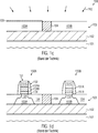
Es zeigt sich jedoch, dass die Fertigungssequenz zum Vorsehen der Schwellwerteinstellung der Halbleiterlegierung deutlich die Schwellwertvariabilität über das Halbleiterchipgebiet hinweg oder über Substrate hinweg beeinflusst, wie dies detaillierter mit Bezug zu den
Das in
Die Transistoren
Obwohl die Schwellwertspannung des p-Kanaltransistors
In der
In der
In der
Angesichts der zuvor beschriebenen Situation betrifft die vorliegende Erfindung Fertigungstechniken für Halbleiterbauelemente, in denen eine effiziente Schwellwerteinstellung auf der Grundlage einer Halbleiterlegierung erreicht wird, die in dem Kanalgebiet vorgesehen wird, wobei eines oder mehrere der oben erkannten Probleme vermieden oder zumindest in der Auswirkung reduziert wird. In view of the situation described above, the present invention relates to fabrication techniques for semiconductor devices in which efficient threshold adjustment is achieved based on a semiconductor alloy provided in the channel region, avoiding or at least reducing in effect one or more of the problems identified above.
Überblick über die vorliegende ErfindungOverview of the present invention
Im Allgemeinen stellt die vorliegende Erfindung Fertigungstechniken bereit, in denen die Schwellwertvariabilität von Transistoren, die eine Schwellwerteinstellung des Halbleiterlegierungsmaterials aufweisen, deutlich verringert wird, indem Prozessungleichmäßigkeiten während des Abscheidens des Schwellwert-einstellenden Halbleitermaterials reduziert werden. Zu diesem Zweck wird der Grad an „Strukturmuster” während des epitaktischen Aufwachsprozesses zum Abscheiden des Schwellwert-einstellenden Halbleitermaterials verringert, wodurch ein hohes Maß an Gleichmäßigkeit über einzelne Halbleiterchipgebiete hinweg und auch über gesamte Substrate hinweg erreicht wird. In dieser Hinsicht ist der Begriff „Strukturmusterbeeinflussung” als die Wirkung der Variabilität der Schichtdicke und/oder Materialzusammensetzung während eines Abscheideprozesses in Abhängigkeit der „Nachbarschaft” des Bereiches zu verstehen, auf welchem das entsprechende Material abzuscheiden ist. Das heißt, typischerweise hängt das Abscheideverhalten von den lokalen Abscheidebedingungen ab, die wiederum durch die Nachbarschaft des Abscheidebereiches bestimmt sind, wobei insbesondere ein ausgeprägter Unterschied zwischen dicht gepackten Bauteilgebieten und nicht-dicht gepackten Bauteilgebieten beobachtet wird. Gemäß den hierin offenbarten Prinzipien können somit die entsprechenden lokalen Abscheidebedingungen gleichmäßiger gestaltet werden, indem das Schwellwert-einstellende Material in einer mehr „globalen” Weise abgeschieden wird und dieses in einer nachfolgenden gleichmäßigen gut steuerbaren Strukturierungssequenz strukturiert wird.In general, the present invention provides fabrication techniques in which the threshold variability of transistors having threshold adjustment of the semiconductor alloy material is significantly reduced by reducing process non-uniformities during deposition of the threshold-adjusting semiconductor material. For this purpose, the degree of "patterning" during the epitaxial growth process for depositing the threshold-adjusting semiconductor material is reduced, thereby achieving a high degree of uniformity across individual semiconductor chip regions and also across entire substrates. In this regard, the term "pattern control" is to be understood as the effect of the variability of the layer thickness and / or material composition during a deposition process as a function of the "proximity" of the region on which the corresponding material is to be deposited. That is, typically, the deposition behavior depends on the local deposition conditions, which in turn are determined by the proximity of the deposition region, and in particular, a pronounced difference is observed between densely packed device regions and non-densely packaged device regions. Thus, in accordance with the principles disclosed herein, the corresponding local deposition conditions may be made more uniform by depositing the threshold adjusting material in a more "global" manner and structuring it in a subsequent uniform well-controllable patterning sequence.
Ein anschauliches hierin offenbartes Verfahren umfasst Bilden eines Schwellwert-einstellenden Halbleitermaterials auf einem ersten und einem zweiten Silizium-enthaltenden Halbleitergebiet;
Einführen einer Dotierstoffsorte in das zweite Silizium-enthaltende Halbleitergebiet unter Anwendung einer Implantationsmaske, die das erste Silizium-enthaltende Halbleitergebiet abdeckt;
Entfernen des Schwellwert-einstellenden Halbleitermaterials selektiv von dem zweiten Silizium-enthaltenden Halbleitergebiet durch Bilden einer Maskenschicht, Strukturieren der Maskenschicht unter Verwendung der genannten Implantationsmaske und Ätzen durch das Schwellwert-einstellenden Halbleitermaterial unter Verwendung der strukturierten Maskenschicht als eine Ätzmaske; und
Bilden einer ersten Gate-Elektrodenstruktur eines ersten Transistors auf dem Schwellwert-einstellenden Halbleitermaterial und einer zweiten Gate-Elektrodenstruktur eines zweiten Transistors auf dem zweiten Silizium-enthaltenden Halbleitergebiet, wobei die erste und die zweite Gate-Elektrodenstruktur ein dielektrisches Material mit großem ε und ein Metall-enthaltendes Elektrodenmaterial aufweisen, das auf dem dielektrischen Material mit großem ε gebildet ist.One illustrative method disclosed herein comprises forming a threshold adjusting semiconductor material on a first and a second silicon-containing semiconductor region;
Introducing a dopant species into the second silicon-containing semiconductor region using an implantation mask covering the first silicon-containing semiconductor region;
Removing the threshold-adjusting semiconductor material selectively from the second silicon-containing semiconductor region by forming a mask layer, patterning the mask layer using said implantation mask, and etching by the threshold-adjusting semiconductor material using the patterned mask layer as an etch mask; and
Forming a first gate electrode structure of a first transistor on the threshold adjusting semiconductor material and a second gate electrode structure of a second transistor on the second silicon-containing semiconductor region, the first and second gate electrode structures being a high-k dielectric material and a metal comprising electrode material formed on the high-k dielectric material.
Kurze Beschreibung der ZeichnungenBrief description of the drawings
Weitere Ausführungsformen der vorliegenden Erfindung und Beispiele, die nicht Bestandteil der vorliegenden Erfindung sind, sind in den angefügten Patentansprüchen definiert und gehen dort aus der folgenden detaillierten Beschreibung hervor, wenn diese mit Bezug zu den begleitenden Zeichnungen studiert wird, in denen:Further embodiments of the present invention and examples, which do not form part of the present invention, are defined in the appended claims, and will become apparent from the following detailed description, when studied with reference to the accompanying drawings, in which:
Detaillierte BeschreibungDetailed description
Im Allgemeinen stellt die vorliegende Erfindung Techniken bereit, in denen komplexe Gate-Elektrodenstrukturen in einer frühen Fertigungsphase auf der Grundlage eines dielektrischen Materials mit großem ε und einem Metall-enthaltenden Elektrodenmaterial hergestellt werden. In diesem Falle kann die Schwellwertspannung eine Art an Transistoren eingestellt werden, indem ein geeignetes Halbleitermaterial in dem Kanalgebiet des jeweiligen Transistors vorgesehen wird, was auf der Grundlage eines Fertigungsprozesses mit besserer Gleichmäßigkeit bewerkstelligt werden kann, wodurch die Schwellwertvariabilität verringert wird, die selbst durch geringe Abweichungen in der Schichtdicke und/oder Materialzusammensetzung von ungefähr ±5% hervorgerufen wird. Das heißt, wie zuvor mit Bezug zu dem Halbleiterbauelement
Der erhöhte Grad an Gleichmäßigkeit wird in einigen anschaulichen Ausführungsformen erreicht, indem die Schwellwert-einstellende Halbleiterlegierung in einer „nicht-selektiven” Weise abgeschieden wird, wobei die Halbleiterlegierung auf aktiven Gebieten jede Art an Transistor abgeschieden wird und nachfolgend von einer Art an Transistoren, etwa von n-Kanaltransistoren, auf der Grundlage eines gut steuerbaren Ätzprozesses abgetragen wird. Es sollte beachtet werden, dass der Begriff „nicht-selektive” Abscheidung auch auf Fälle zutrifft, in denen dennoch ein Grad an Flexibilität zwischen kristallinen Halbleiteroberflächen und dielektrischen Oberflächenbereichen erreicht wird, die etwa in Form von Isolationsstrukturen und dergleichen vorgesehen sind. Selbst wenn eine Abscheidung der Halbleiterlegierung auf kristalline Halbleiteroberflächen beschränkt wird, können somit deutlich bessere Abscheidebedingungen über den gesamten Halbleiterchip hinweg oder das Substrat hinweg, das eine Vielzahl von Halbleiterchips aufweisen kann, erreicht, da auf lokalem Maßstab sehr ähnliche Abscheidebedingungen erreicht werden, da typischerweise beide Transistorarten in unmittelbarer Nähe zueinander positioniert sind, unabhängig davon, ob dicht gepackte oder nicht-dicht gepackte Bauteilgebiete betrachtet werden. In anderen anschaulichen Ausführungsform werden die Isolationsstrukturen hergestellt, nachdem die Halbleiterlegierung in einer sehr nicht-selektiven Weise abgeschieden wird, wodurch die Gleichmäßigkeit der Abscheidebedingungen noch weiter verbessert wird. In einigen anschaulichen hierin offenbarten Ausführungsformen wird die Strukturierung der Halbleiterlegierung bewerkstelligt, ohne dass ein zusätzlicher Lithografieschritt erforderlich ist, wodurch für einen effizienten gesamten Fertigungsablauf gesorgt wird.The increased degree of uniformity is achieved in some illustrative embodiments by depositing the threshold-adjusting semiconductor alloy in a "non-selective" manner, wherein the semiconductor alloy is deposited on active regions of each type of transistor and subsequently on one type of transistors, such as transistors of n-channel transistors, is removed on the basis of a well controllable etching process. It should be noted that the term "non-selective" deposition also applies to cases in which, nevertheless, a degree of flexibility is achieved between crystalline semiconductor surfaces and dielectric surface regions, for instance in the form of insulating structures and the like. Thus, even if deposition of the semiconductor alloy is limited to crystalline semiconductor surfaces, significantly better deposition conditions can be achieved across the entire semiconductor chip or substrate, which may comprise a plurality of semiconductor chips, since very similar deposition conditions are achieved on a local scale, since typically both Transistor types are positioned in close proximity to each other, regardless of whether densely packed or non-densely packed component areas are considered. In other illustrative embodiments, the isolation structures are formed after the semiconductor alloy is deposited in a very non-selective manner, thereby further improving the uniformity of the deposition conditions. In some illustrative embodiments disclosed herein, the patterning of the semiconductor alloy is accomplished without the need for an additional lithography step, thereby providing an efficient overall manufacturing process.
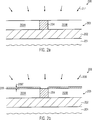
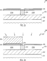
Mit Bezug zu den
Im Hinblick auf die bislang beschriebenen Komponenten und in Bezug auf entsprechende Fertigungstechniken zur Herstellung dieser Komponenten gelten die gleichen Kriterien, wie zuvor mit Bezug zu dem Halbleiterbauelement
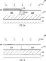
Mit Bezug zu den
Die Transistoren
Es gilt also: die vorliegende Erfindung stellt Fertigungstechniken bereit, in denen mit der Abscheidung in Beziehung stehende Ungleichmäßigkeiten für die Herstellung einer Schwellwert-einstellenden Halbleiterlegierung verringert werden, indem das Material auf aktiven Gebieten für jede Art von Transistor abgeschieden wird und nachfolgend die Halbleiterlegierung auf der Grundlage einer gut steuerbaren Strukturierungssequenz strukturiert wird. Folglich können aufwändige Gate-Elektrodenstrukturen mit dielektrischem Material mit großem ε und mit einem Metall-enthaltenden Elektrodenmaterial in einer frühen Fertigungsphase hergestellt werden, d. h. vor der Erzeugung der Drain- und Source-Gebiete, auf der Grundlage einer Schwellwert-einstellenden Halbleiterlegierung, etwa eines Silizium/Germaniummaterials, wobei die bessere Gleichmäßigkeit während der selektiven Herstellung des Schwellwert-einstellenden Materials zu einer geringeren Schwellwertvariabilität führt, selbst wenn äußerst größenreduzierte Halbleiterbauelemente betrachtet werden.Thus, the present invention provides fabrication techniques in which deposition-related non-uniformities for the fabrication of a threshold-adjusting semiconductor alloy are reduced by depositing the material in active regions for each type of transistor and subsequently depositing the semiconductor alloy onto the semiconductor device Basis of a well-controllable structuring sequence is structured. Consequently, expensive gate electrode structures with high-k dielectric material and with a metal-containing electrode material can be fabricated in an early manufacturing stage, i. H. prior to the generation of the drain and source regions, based on a threshold-adjusting semiconductor alloy, such as a silicon germanium material, wherein the improved uniformity during selective fabrication of the threshold adjusting material results in lower threshold variability, even if highly scaled semiconductor devices to be viewed as.
Claims (6)
Priority Applications (6)
| Application Number | Priority Date | Filing Date | Title |
|---|---|---|---|
| DE102008063402A DE102008063402B4 (en) | 2008-12-31 | 2008-12-31 | Reducing the threshold voltage fluctuation in transistors with a channel semiconductor alloy by reducing the deposition nonuniformities |
| US12/637,112 US8236654B2 (en) | 2008-12-31 | 2009-12-14 | Reduction of threshold voltage variation in transistors comprising a channel semiconductor alloy by reducing deposition non-uniformities |
| JP2011542725A JP5669752B2 (en) | 2008-12-31 | 2009-12-29 | Reducing threshold voltage variation by reducing deposition non-uniformity in transistors with channel semiconductor alloys |
| KR1020117018048A KR101539416B1 (en) | 2008-12-31 | 2009-12-29 | Reduction of threshold voltage variation in transistors comprising a channel semiconductor alloy by reducing deposition non-uniformities |
| CN200980157723.XA CN102341906B (en) | 2008-12-31 | 2009-12-29 | Reduction of threshold voltage variation in transistors comprising a channel semiconductor alloy by reducing deposition non-uniformities |
| PCT/EP2009/009307 WO2010076018A1 (en) | 2008-12-31 | 2009-12-29 | Reduction of threshold voltage variation in transistors comprising a channel semiconductor alloy by reducing deposition non-uniformities |
Applications Claiming Priority (1)
| Application Number | Priority Date | Filing Date | Title |
|---|---|---|---|
| DE102008063402A DE102008063402B4 (en) | 2008-12-31 | 2008-12-31 | Reducing the threshold voltage fluctuation in transistors with a channel semiconductor alloy by reducing the deposition nonuniformities |
Publications (2)
| Publication Number | Publication Date |
|---|---|
| DE102008063402A1 DE102008063402A1 (en) | 2010-07-08 |
| DE102008063402B4 true DE102008063402B4 (en) | 2013-10-17 |
Family
ID=42234616
Family Applications (1)
| Application Number | Title | Priority Date | Filing Date |
|---|---|---|---|
| DE102008063402A Active DE102008063402B4 (en) | 2008-12-31 | 2008-12-31 | Reducing the threshold voltage fluctuation in transistors with a channel semiconductor alloy by reducing the deposition nonuniformities |
Country Status (6)
| Country | Link |
|---|---|
| US (1) | US8236654B2 (en) |
| JP (1) | JP5669752B2 (en) |
| KR (1) | KR101539416B1 (en) |
| CN (1) | CN102341906B (en) |
| DE (1) | DE102008063402B4 (en) |
| WO (1) | WO2010076018A1 (en) |
Families Citing this family (8)
| Publication number | Priority date | Publication date | Assignee | Title |
|---|---|---|---|---|
| DE102009006886B4 (en) * | 2009-01-30 | 2012-12-06 | Advanced Micro Devices, Inc. | Reducing thickness variations of a threshold adjusting semiconductor alloy by reducing the patterning non-uniformities before depositing the semiconductor alloy |
| JP5605134B2 (en) * | 2010-09-30 | 2014-10-15 | 富士通セミコンダクター株式会社 | Semiconductor device and manufacturing method thereof |
| DE102010063296B4 (en) * | 2010-12-16 | 2012-08-16 | Globalfoundries Dresden Module One Limited Liability Company & Co. Kg | Production method with reduced STI topography for semiconductor devices with a channel semiconductor alloy |
| US8609509B2 (en) | 2011-09-22 | 2013-12-17 | Globalfoundries Inc. | Superior integrity of high-k metal gate stacks by forming STI regions after gate metals |
| US8377773B1 (en) * | 2011-10-31 | 2013-02-19 | Globalfoundries Inc. | Transistors having a channel semiconductor alloy formed in an early process stage based on a hard mask |
| US8541281B1 (en) | 2012-08-17 | 2013-09-24 | Globalfoundries Inc. | Replacement gate process flow for highly scaled semiconductor devices |
| US8969190B2 (en) | 2012-08-24 | 2015-03-03 | Globalfoundries Inc. | Methods of forming a layer of silicon on a layer of silicon/germanium |
| US9029919B2 (en) | 2013-02-01 | 2015-05-12 | Globalfoundries Inc. | Methods of forming silicon/germanium protection layer above source/drain regions of a transistor and a device having such a protection layer |
Citations (6)
| Publication number | Priority date | Publication date | Assignee | Title |
|---|---|---|---|---|
| US20050136624A1 (en) * | 2001-04-04 | 2005-06-23 | Massachusetts Institute Of Technology | Method for semiconductor device fabrication |
| WO2005067055A1 (en) * | 2003-12-24 | 2005-07-21 | Intel Corporation | Transistor gate electrode having conductor material layer |
| US7217608B1 (en) * | 2001-12-17 | 2007-05-15 | Advanced Micro Devices, Inc. | CMOS with strained silicon channel NMOS and silicon germanium channel PMOS |
| US20080079086A1 (en) * | 2006-08-10 | 2008-04-03 | Hyung-Suk Jung | Semiconductor device and method of manufacturing the same |
| US20080111155A1 (en) * | 2006-11-14 | 2008-05-15 | Freescale Semiconductor, Inc. | Electronic device including a transistor having a metal gate electrode and a process for forming the electronic device |
| WO2008112949A1 (en) * | 2007-03-15 | 2008-09-18 | Intel Corporation | Cmos device with dual-epi channels and self-aligned contacts |
Family Cites Families (27)
| Publication number | Priority date | Publication date | Assignee | Title |
|---|---|---|---|---|
| KR100473901B1 (en) * | 1995-12-15 | 2005-08-29 | 코닌클리케 필립스 일렉트로닉스 엔.브이. | Semiconductor Field Effect Device Including SiGe Layer |
| JP2000353753A (en) * | 1999-06-14 | 2000-12-19 | Hitachi Ltd | Manufacture of semiconductor device |
| AU2002306436A1 (en) * | 2001-02-12 | 2002-10-15 | Asm America, Inc. | Improved process for deposition of semiconductor films |
| JP2004006959A (en) * | 2001-04-12 | 2004-01-08 | Matsushita Electric Ind Co Ltd | Semiconductor device and manufacturing method thereof |
| US6794252B2 (en) * | 2001-09-28 | 2004-09-21 | Texas Instruments Incorporated | Method and system for forming dual work function gate electrodes in a semiconductor device |
| CN100399576C (en) * | 2002-03-28 | 2008-07-02 | 先进微装置公司 | Semiconductor device having a retrograde dopant profile in a channel region and method for fabricating the same |
| KR100487525B1 (en) * | 2002-04-25 | 2005-05-03 | 삼성전자주식회사 | Semiconductor device using silicon-germanium gate and method for fabricating the same |
| JP2003332458A (en) * | 2002-05-09 | 2003-11-21 | Fujitsu Ltd | Semiconductor device and its manufacturing method |
| KR20030090411A (en) * | 2002-05-23 | 2003-11-28 | 삼성전자주식회사 | CMOS gate electrode using selective growth and fabrication method the same |
| EP1588416B1 (en) * | 2003-01-07 | 2009-03-25 | S.O.I.Tec Silicon on Insulator Technologies | Recycling of a wafer comprising a multi-layer structure after taking-off a thin layer |
| US6828181B2 (en) * | 2003-05-08 | 2004-12-07 | International Business Machines Corporation | Dual gate material process for CMOS technologies |
| CN100536167C (en) * | 2003-08-05 | 2009-09-02 | 富士通微电子株式会社 | Semiconductor device and preparation method thereof |
| CN1906755A (en) * | 2004-04-30 | 2007-01-31 | 松下电器产业株式会社 | Semiconductor manufacturing method and semiconductor device |
| JP2008513979A (en) * | 2004-09-14 | 2008-05-01 | アリゾナ ボード オブ リージェンツ ア ボディー コーポレート アクティング オン ビハーフ オブ アリゾナ ステイト ユニバーシティ | Si-Ge semiconductor material and device growth method on a substrate |
| JP2006108251A (en) * | 2004-10-01 | 2006-04-20 | Rohm Co Ltd | Manufacturing method of semiconductor device |
| JP2006202928A (en) * | 2005-01-19 | 2006-08-03 | Nec Electronics Corp | Method of manufacturing semiconductor device |
| US7132322B1 (en) * | 2005-05-11 | 2006-11-07 | International Business Machines Corporation | Method for forming a SiGe or SiGeC gate selectively in a complementary MIS/MOS FET device |
| TWI267926B (en) * | 2005-09-23 | 2006-12-01 | Ind Tech Res Inst | A new method for high mobility enhancement strained channel CMOS with single workfunction metal-gate |
| JP4795817B2 (en) * | 2006-03-02 | 2011-10-19 | 富士通セミコンダクター株式会社 | Manufacturing method of semiconductor device |
| JP2006332687A (en) * | 2006-07-10 | 2006-12-07 | Fujitsu Ltd | Cmos semiconductor device |
| KR100773359B1 (en) * | 2006-11-20 | 2007-11-05 | 삼성전자주식회사 | Fabrication method of transistors having a high mobility and transistors fabricated thereby |
| JP4898517B2 (en) * | 2007-03-27 | 2012-03-14 | シャープ株式会社 | Manufacturing method of semiconductor device |
| US7709331B2 (en) * | 2007-09-07 | 2010-05-04 | Freescale Semiconductor, Inc. | Dual gate oxide device integration |
| US20090108294A1 (en) * | 2007-10-30 | 2009-04-30 | International Business Machines Corporation | Scalable high-k dielectric gate stack |
| US7718496B2 (en) * | 2007-10-30 | 2010-05-18 | International Business Machines Corporation | Techniques for enabling multiple Vt devices using high-K metal gate stacks |
| US8053306B2 (en) * | 2007-12-13 | 2011-11-08 | International Business Machines Corporation | PFET with tailored dielectric and related methods and integrated circuit |
| JP2010157570A (en) * | 2008-12-26 | 2010-07-15 | Toshiba Corp | Method of manufacturing semiconductor device |
-
2008
- 2008-12-31 DE DE102008063402A patent/DE102008063402B4/en active Active
-
2009
- 2009-12-14 US US12/637,112 patent/US8236654B2/en active Active
- 2009-12-29 CN CN200980157723.XA patent/CN102341906B/en active Active
- 2009-12-29 JP JP2011542725A patent/JP5669752B2/en active Active
- 2009-12-29 WO PCT/EP2009/009307 patent/WO2010076018A1/en active Application Filing
- 2009-12-29 KR KR1020117018048A patent/KR101539416B1/en not_active IP Right Cessation
Patent Citations (6)
| Publication number | Priority date | Publication date | Assignee | Title |
|---|---|---|---|---|
| US20050136624A1 (en) * | 2001-04-04 | 2005-06-23 | Massachusetts Institute Of Technology | Method for semiconductor device fabrication |
| US7217608B1 (en) * | 2001-12-17 | 2007-05-15 | Advanced Micro Devices, Inc. | CMOS with strained silicon channel NMOS and silicon germanium channel PMOS |
| WO2005067055A1 (en) * | 2003-12-24 | 2005-07-21 | Intel Corporation | Transistor gate electrode having conductor material layer |
| US20080079086A1 (en) * | 2006-08-10 | 2008-04-03 | Hyung-Suk Jung | Semiconductor device and method of manufacturing the same |
| US20080111155A1 (en) * | 2006-11-14 | 2008-05-15 | Freescale Semiconductor, Inc. | Electronic device including a transistor having a metal gate electrode and a process for forming the electronic device |
| WO2008112949A1 (en) * | 2007-03-15 | 2008-09-18 | Intel Corporation | Cmos device with dual-epi channels and self-aligned contacts |
Also Published As
| Publication number | Publication date |
|---|---|
| JP2012514318A (en) | 2012-06-21 |
| DE102008063402A1 (en) | 2010-07-08 |
| KR20120067973A (en) | 2012-06-26 |
| US8236654B2 (en) | 2012-08-07 |
| JP5669752B2 (en) | 2015-02-18 |
| KR101539416B1 (en) | 2015-07-27 |
| WO2010076018A1 (en) | 2010-07-08 |
| CN102341906B (en) | 2014-10-15 |
| CN102341906A (en) | 2012-02-01 |
| US20100164014A1 (en) | 2010-07-01 |
Similar Documents
| Publication | Publication Date | Title |
|---|---|---|
| DE102009015747B4 (en) | A method of fabricating transistors having metal gate electrode structures and high-k gate dielectric and an intermediate etch stop layer | |
| DE102009010883B4 (en) | Adjusting a non-silicon content in a semiconductor alloy during FET transistor fabrication by an intermediate oxidation process | |
| DE102009021489B4 (en) | Increasing deposition uniformity for a semiconductor alloy provided for threshold adjustment in an active region | |
| DE102009006886B4 (en) | Reducing thickness variations of a threshold adjusting semiconductor alloy by reducing the patterning non-uniformities before depositing the semiconductor alloy | |
| DE102011077661B4 (en) | Metal gate electrode structures and methods of making same by reducing the gate fill aspect ratio in a replacement gate technology | |
| DE102007063270B4 (en) | A method of reducing the generation of charge trapping sites in gate dielectrics in MOS transistors by performing a hydrogen treatment | |
| DE102008064671B4 (en) | A method of fabricating a semiconductor device having a gate structure and increasing the integrity of a high-k gate stack by protecting a coating on the gate bottom during exposure of the gate top | |
| DE102009006802B3 (en) | A method and semiconductor device with work function adjustment in a high ε gate electrode structure after transistor fabrication using lanthanum | |
| DE102009010847B4 (en) | Integrate semiconductor alloys into PMOS and NMOS transistors using a common recess etch process | |
| DE102008063402B4 (en) | Reducing the threshold voltage fluctuation in transistors with a channel semiconductor alloy by reducing the deposition nonuniformities | |
| DE102009031110B4 (en) | Improved cover layer integrity in a gate stack by using a hard mask for spacer patterning | |
| DE102010063296B4 (en) | Production method with reduced STI topography for semiconductor devices with a channel semiconductor alloy | |
| DE102009006801B4 (en) | A method of fabricating a field effect short channel transistor having less length fluctuation by using an amorphous electrode material during implantation | |
| DE102009021484B4 (en) | Greater uniformity of a channel semiconductor alloy by producing STI structures after the growth process | |
| DE102009035418B4 (en) | Producing a channel semiconductor alloy by depositing a hard mask for selective epitaxial growth | |
| DE102008063432B4 (en) | A method of adjusting the strain caused in a transistor channel of a FET by semiconductor material provided for threshold adjustment | |
| DE102010028459B4 (en) | Reduced STI topography in high-G metal gate transistors by using a mask after deposition of a channel semiconductor alloy | |
| DE102010064291A1 (en) | Transistors having large ε metal gate electrode structures comprising a polycrystalline semiconductor material and embedded strain-inducing semiconductor alloys | |
| DE102013206295B4 (en) | Method of fabricating FET transistor elements with higher stability of the transistor properties in early formed high-k / metal gate | |
| DE102010063774A1 (en) | Production of a channel semiconductor alloy by means of a nitride hard mask layer and an oxide mask | |
| DE102009055395B4 (en) | Pre-doped semiconductor material for a large gate metal gate electrode structure of p and n channel transistors | |
| DE102011090169A1 (en) | Structuring of sensitive metal-containing layers with increased mask material adhesion by providing a modified surface layer | |
| DE102009010846B4 (en) | A method of fabricating a high-ε gate electrode structure to increase its integrity by including a metal capping layer after deposition | |
| DE102009047311B4 (en) | A method for producing gate structures with improved interface properties between a channel semiconductor alloy and a gate dielectric by means of an oxidation process | |
| DE102009055394B4 (en) | A method and semiconductor device with enhancement of deposition uniformity for a channel semiconductor alloy by forming a well prior to well implantation |
Legal Events
| Date | Code | Title | Description |
|---|---|---|---|
| OP8 | Request for examination as to paragraph 44 patent law | ||
| R016 | Response to examination communication | ||
| R016 | Response to examination communication | ||
| R130 | Divisional application to |
Ref document number: 102008064796 Country of ref document: DE Effective date: 20130409 |
|
| R018 | Grant decision by examination section/examining division | ||
| R020 | Patent grant now final |
Effective date: 20140118 |
|
| R081 | Change of applicant/patentee |
Owner name: ADVANCED MICRO DEVICES, INC., SANTA CLARA, US Free format text: FORMER OWNERS: ADVANCED MICRO DEVICES, INC., SUNNYVALE, CALIF., US; AMD FAB 36 LIMITED LIABILITY COMPANY & CO. KG, 01109 DRESDEN, DE |
|
| R082 | Change of representative |
Representative=s name: GRUENECKER PATENT- UND RECHTSANWAELTE PARTG MB, DE |