EP0010791A1 - Method and device for inspecting a moving sheet material for streaklike defects - Google Patents
Method and device for inspecting a moving sheet material for streaklike defects Download PDFInfo
- Publication number
- EP0010791A1 EP0010791A1 EP79200564A EP79200564A EP0010791A1 EP 0010791 A1 EP0010791 A1 EP 0010791A1 EP 79200564 A EP79200564 A EP 79200564A EP 79200564 A EP79200564 A EP 79200564A EP 0010791 A1 EP0010791 A1 EP 0010791A1
- Authority
- EP
- European Patent Office
- Prior art keywords
- signal
- signals
- scanning
- sheet material
- ratio
- Prior art date
- Legal status (The legal status is an assumption and is not a legal conclusion. Google has not performed a legal analysis and makes no representation as to the accuracy of the status listed.)
- Granted
Links
Images


Classifications
-
- G—PHYSICS
- G01—MEASURING; TESTING
- G01N—INVESTIGATING OR ANALYSING MATERIALS BY DETERMINING THEIR CHEMICAL OR PHYSICAL PROPERTIES
- G01N21/00—Investigating or analysing materials by the use of optical means, i.e. using sub-millimetre waves, infrared, visible or ultraviolet light
- G01N21/84—Systems specially adapted for particular applications
- G01N21/88—Investigating the presence of flaws or contamination
- G01N21/89—Investigating the presence of flaws or contamination in moving material, e.g. running paper or textiles
- G01N21/892—Investigating the presence of flaws or contamination in moving material, e.g. running paper or textiles characterised by the flaw, defect or object feature examined
- G01N21/8921—Streaks
Definitions
- This invention relates to a method and a device for inspecting a moving sheet material for streaklike defects, comprising means for directing radiant energy on one surface of the sheet material and photocell means for measuring at distinct lateral positions of the sheet material the intensity of the radiation after transmission of the radiation through, or after reflection on the surface of the sheet material.
- Known devices operate satisfactorily for the detection of rather coarse speck- and streaklike defects in moving sheets since in such cases the signal-to-noise ratio of the output signals of the photocells is sufficiently great to enable the signals, after their amplification, to be compared with a predetermined reference signal in order to identify a defect.
- Suchlike defect identifying signals may either be stored in digital or analogue form in a memory together with the exact address of the defect, or they may directly be signalled as in the coating of webs in order to arrest or to re-adjust the coating, or they may directly control a sorting mechanism as in the inspection of sheets cut from a coated web.
- specklike defects caused by the inclusion of a strange object, e.g. a dust particle in a coated layer, or a dry spot, e.g. an air bubble included during the coating of a layer on a support.
- S/N ratio signal-to-noise ratio
- a basic condition for the operation of such techniques is that the defect to be identified should be recursive during a number of, say at least 5, successive scans. This means that the defects have to be of protracted duration in the machine direction, that is in the coating direction in the case of the inspection of coated layers. In other words, only streaklike defect signals are suitable for S/N ratio improvement.
- the time t of the correlation circuit for reaching a significant S/N ratio improvement is rather important so that in some cases it may take up to 100 seconds and more before the correlated signal is available. It is the object of the invention to provide a new correlation technique in the inspection of a moving sheet material for streaklike defects, that does not show the shortcomings mentioned hereinbefore.
- the invention aims in particular at considerably improving the S/N ratio of photocell signals that are encountered in the identification of very subtle streaklike defects in moving sheet materials.
- streaklike irregularities may be mentioned that occur at the coating on a web of a layer, or of a combination of layers as the case may be, by means of a so-called cascade or slide hopper coater.
- cascade or slide hopper coater In certain application fields, notably in photography, very stringent requirements are put to the uniformity of a coated layer, and it is shown that defect signals resulting from streaklike thickness deviations of an order of magnitude under 0.1 %, even when additively correlated, are not discernable from the noise component of the signals.
- a method for inspecting at least one longitudinal section of a moving sheet material for streaklike defects by repeatedly transversely scanning said at least one section of the material by means of radiant energy capable of being modulated by said sheet material, and by receiving said modulated energy on at least one photocell thereby to detect at said at least one photocell signals that are periodically recurring in response with the scanning of the material and the variation of which signals is indicative of the presence of said defects, comprises improving the S/N ratio of those said periodically recurring signals the S/N ratio of which is greater than one, by delaying each measurement signal V m over a delay time t corresponding with the scanning period P, multiplying a next signal V with a factor that is proportional to the product of said delayed signal and a factor A, delaying said multiplied signal over said delay time t and multiplying the next signal V m with a factor that is proportional to the product of said previous multiplied signal and said factor A, and so on for a number of times, wherein said factor A is at least equal to
- sheet material stands for webs that may have a length up to many hundreds of meters, as well as for a plurality of distinct sheets that may have been cut from such webs and that may be inspected in succession.
- modulated by indicates that radiation is attenuated on its path towards the photocell, either by transmission through the sheet material or by reflection from the surface of said sheet material. Said defects modify the attenuation.
- signals with a S/N ratio greater than. one means in the present specification signals the defect- component of which is greater than the effective noise component. This means that peak-to-peak noise levels may be present in the photocell signal that are much greater than the useful signal level but the effective value of which, that is the rms value determined over a time that is equal to the quotient of the scanning time t by the number of discrete measurements during said time.
- the scanning period "P" is the time comprised between two successive scans of a given zone of said at least one longitudinal section from edge to edge in one direction.
- the measurement signal V may be the output signal of a photocell that must be compared with a given reference signal in order to establish the occasional deviation of said measurement signal, thereby to detect a defect at the lateral position of the sheet material inspected by the photocell, but said signal V may also be, and in a different embodiment preferably is, the difference, amplified as the case may be, between two successive signals of a multiplicity of sequential output signals that represent the scanning of the sheet material.
- scanning stands for the repeated inspection of the sheet material in a direction that runs transverse with respect to the direction of movement of the sheet material.
- the scanning may occur by means of a beam of radiation that is projected on the sheet material and that is swept over the material.
- This sweeping may be done by means of a source of radiation mounted on a frame arranged for oscillation transverse with respect to the material, but said sweeping may also be carried out by means of a beam of radiation that is deflected by a rotating or pivoting mirror or the like.
- the scanning may occur by means of a plurality of distinct small light sources, for instance light emitting diodes (LED's) that are mounted closely adjacent to each other in a row and that may be energized in sequence to produce a radiation spot that scans the sheet material.
- LED's light emitting diodes
- the photocell may be arranged for lateral displacement synchronous with the scanning beam of radiation, but the photocell may also collect, for instance by means of a collecting glass rod that extends transversely of the sheet material, the radiant energy that has been modulated by the sheet material.
- a plurality of photocells may be mounted in a row extending transversely of the web path for receiving radiant energy that has been modulated by the zone of the sheet section that corresponds with the field angle of a corresponding photocell.
- a multiplicity of successive measurements are carried out during each scanning, each two successive measurement signals are compared with each other, and the difference between each such two successive signals constitutes the signal m.
- a device in accordance with the present invention comprises :
- Figure 1 is a diagrammatic isometric view of a device for transversely scanning a moving web.
- the device comprises a boxlike frame 20 that is slideably suspended by means of two guides 21 and 22 on two horizontally spaced, fixed parallel rods 23 and 24.
- suspension means may be replaced by any known other suspension or guide mechanism that enables the frame to carry out a scanning movement in the direction indicated by the arrow 25.
- the transverse position of the frame with respect to a web 10 that is advanced in the direction of the arrow 11 is controlled by a crank 26 that is pivotally fitted to one end of the frame and to a drive wheel 27 that may continuously rotate at a constant speed.
- the web 10 is passed through the device through a slotlike opening 28 along a path that is determined by the tangent plane to two rollers (not shown), one being located upstream and the other downstream of the device.
- the unit comprises two so-called fishtail optics 29 and 30 which are fiber optic assemblies wherein the fibers are bundled at one extremity to a bundle with a circular cross-section, and wherein the fibers diverge towards the other extremity to form a line on which the single fibers are ranged closely adjacent to each other.
- the two fishtail assemblies have been ground at their. lower ends to form an interface 31 at which they are adhered to each other.
- a rodlike lens 32 with a semicircular cross-section projects the lines of radiation at the lower ends of the fishtail optics on the web in the form of the two narrow elongate beams of radiant energy hereinafter called "lines", that have been represented by the solid points 33 and 34, respectively.
- the radiant energy may be produced by any suitable source such as an incandescent bulb, a light-emitting diode (LED),'or the like.
- a light-emitting diode LED
- two LED's 95 and 96 were placed in face of the upper ends of the corresponding fishtail optics.
- Radiation from both lines 33 and 34 that is transmitted through the web may be bundled by a second rodlike lens, such as lens 35 onto an elongate photocell 36.
- the sources of radiation as well as the photocell carry out an oscillating motion as indicated by the arrows 25.
- the amplitude of said oscillation is that of the oscillating amplitude of the frame 20 shown in fig. 3.
- the electronic block circuit of the device is shown in fig. 4.
- a web 10 that moves in a direction normal to the plane of the drawing is scanned by pairs of light sources 95 and 96 that produce adjacent pairs of lines of radiant energy on the web as shown in detail in fig. 2.
- Corresponding photocells 18 receive the radiation transmitted through the web and are bodily coupled as illustrated by the broken lines 40 and 41 with the light sources in order to carry out an oscillating displacement with respect to the web in the direction of the arrow 25.
- Both light sources of each pair of sources are alternatively energized by a source 42 in response to an oscillator 43.
- the output signals V of the photocells are amplified by amplifiers 44 and synchronously demodulated by corresponding demodulators 45 that are likewise controlled by the oscillator 43.
- the amplifiers 44 may comprise a high-pass filter with a breakpoint at 20 Hz for 6 db attenuation.
- the frame of the device is further provided with a pulse-generator 46 in the form of a glass strip that is provided with a great number of spaced fields capable of periodically absorbing the radiation from a stationary light source 47 that is directed to a photocell 48.
- the vertical dash and dot line 49 represents a wall of the oscillating frame at which all electric terminals 50 may be grouped and connected by means of a flexible band comprising different separate conductors with the remaining electronic circuit of the device which in practice is mounted in a stationary column beside the oscillating frame.
- this distance c is a fraction only of the peak to peak amplitude of the oscillation of the frame 20. This is illustrated in the diagram of fig. 5 wherein the distance d represents the peak to peak amplitude of the frame 20, whereas the distance c represents the effective scanning width of each photocell. As a consequence of the mentioned difference between d and c, the distance c covers a portion of the curve 51 that represents the sinusoidal motion of the frame, that deviates not quite much from a line, whereby the corresponding speed of the frame during measuring is nearly uniform.
- the right hand portion of the drawing of fig. 4 shows a known additive correlation circuit for improving the S/N ratio of the measurement signals V. It should be noted that actually there is one such correlation circuit for each photocell circuit.
- the electronic correlation circuit comprises an adder- type amplifier 52, an analogue to digital converter 53, a delay line 54 in the form of an 8 bit shift register with 1024 positions, a digital to analogue converter 55, and feedback element 56.
- the adder sums the incoming signals V i with a delayed output signal V 0 which has been multiplied by a feedback gain which is strictly less than unity.
- the delay line 54 is controlled in synchronism with the scanning of the web by pulses produced by the pulse generating strip 46 that comprises in this specific embodiment 1024 pairs of light absorbing and light transmission areas.
- the signals of the photocell 48 ' are appropriately shaped by a pulse shaper 57.
- the operation of the circuit is as follows. An input signal that occurs at a time t 1 , see fig. 5, is stored in the first stage of the shift register 54 until at a time t 2 the pulse generator 46 controls the shift register to shift its information over one place whereby the first signal is transferred to a second position, and the new signal that occurs at the time t 2 is entered into the shift register. The same procedure continues until the generator 46 has been displaced over a distance c i.e. at the time t 1024 which means that the scanning of the respective section of the web has been completed.
- the circuit is so arranged (not illustrated) that during the returning movement of the frame the shift registers remain inoperative.
- a pulse from the generator 46 at a time t 1 transfers the signal of the shift register that is at the position 1024 to the position 1 whereby (through 55, 56, 52 and 53) said signal is added to the next signal that occurs at the same transverse zone of the web as the zone where said transferred signal occurred, etc.
- the same operation is repeated a number of times thereby to increase the S/N ratio of each of the signals at the positions from 1 to 1024 by a factor as will further be explained.
- each correlator circuit is fed to a trigger 58 where they are compared with a reference signal from a reference signal generator 59.
- the output signal at terminal 63 may, either directly control a warning mechanism, or it may be stored either in analogue or in converted digital form in a memory together with the exact address of the location of the defect on the web.
- One part of said address is formed by the pulse number of the generator 46 which indicates the transverse location of the defect on the web.
- Another part of the address may be formed by the number from a counter that counts the number of meters of the web which have been unwound from a roll.
- Such counter is usually reset at zero at the starting of the treatment, for example coating, of each new web roll. Still another part of the address may be formed by an identification number for the device that detected the object.
- the circuit comprises further a second trigger 61 that is directly connected with the input terminal 50 and that serves for the instant signalling at a terminal 62 of defects that are so severe that they need not a repeated circulation through the correlation circuit, with the corresponding delay, to reach a level at which sufficient signal to noise distinction has been obtained.
- the active operation of the device namely from a time t 1 to a time t 1024 , is a fraction only of the period of one complete scanning.
- the examination of the moving web occurs in consequence interruptedly considered in the longitudinal direction. Taking into account however, that the device according to the invention is intended for the identification of streaklike defects of protracted duration, this lack of continuity of the measurement in the longitudinal direction of the web is without any importance.
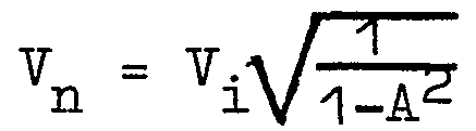
- the circuit comprises an adder 67, a delay line 68 with a delay time z and an adjustable feedback element 69 with a gain A comprised between 0 and 1. It can be shown that the relation between the output voltage V 0 and the input voltage V i is expressed by : and that the improvement of the S/N ratio is : or, expressed in db : (2)
- the system reaches 99 % of its maximum S/N improvement after a time t given by :
- the S/N improvement amounts to a ratio of 14.106.
- the abscissa is a time axis in seconds whereas the ordinate represents V.
- the maximum level of the noise component V n of the output signal V 0 after 100 s has been arbitrarily illustrated at a level of 1 volt. In fact whereas . It may be seen that both the noise signal V n and the defect signal V d exponentially increase in the same direction towards a determined limit.
- the S/N ratio of periodically recurring signals is improved by multiplicatively correlating said signals instead of additively correlating them.
- the basic operation of multiplicative correlation is illustrated in fig. 8 wherein the block circuit comprises a multiplicator 70, a delay line 71 with a delay time ⁇ , and a feedback element 72 with a gain factor A. It can be shown that the relation between the output voltage V o and the input voltage V i is expressed 1031 by:
- the system produces a S/N improvement that is infinitely great in theory.
- said improvement is limited by the maximal level the signal component V d can reach in the circuit. Common values for said signal Vd are within 12 and 15 volts in modern integrated circuit lay-outs.
- a basic condition for the operation of the described circuit is that the product of the input signal V i with its delayed equivalent is always greater than one. In case said product is smaller than one, then repeated multiplication will only reduce the amplitude of the signal instead of increasing it.
- the mentioned condition may be met in one of two ways : either the signal V i is greater than 1 volt and in that case the gain A may be equal to one, or the signal V i is smaller than one volt and in that case the gain A is adjusted so that the product V i .
- A is greater than 1.
- Another basic condition for the operation of the circuit is that the ratio of the useful signal level V d to the effective noise level V n of the input voltage V i be greater than one. Otherwise the system is incapable of making a-distinction between signal and noise.
- Fig. 10 is a block circuit of a multiplicative correlator wherein common integrated circuits are used.
- a multiplier 75 (type 8013 manufactured by Intersil Corp.) is followed by an analogue to digital convertor 76 (type AD 7570 manufactured by Analog Devices), a digital 8-bits shift register 77 (type SY 2533 manufactured by Synertek) and a digital to analogue convertor 77 (type AD 559 manufactured by Analog Devices).
- the circuit comprises further an analogue adder 79 (type ⁇ A 741 manufactured by Fairchild) for adding to the output voltage V o a small voltage V a that may be set by means of a potentiometer 80.
- V a The purpose of said voltage V a is as follows. At the starting of a correlation cycle, it may occur that, depending on the offset characteristics of the convertor 78, that the output voltage V o is zero. The repeated multiplication of V by V i will involve no result since multiplication by a factor zero gives a product that remains zero.
- V a a given voltage V a is added to the voltage V o before the multiplication with V i occurs.
- Said voltage V a may be small since its only purpose is to make sure that V i will not become multiplied by zero.
- V a will be chosen between 100 and 200 mV for a full scale output voltage of the device of 10 V. It is clear that the addition of said voltage V a "falsifies” so to say the correlated output signal V o . It should be understood, however, that this "falsification” is neglectable as compared by the distortion of the signal V i as a consequence of the multiplicative correlation.
- any signal V i that comprises a signal component greater than 1 volt and a noise component smaller than 1 volt inevitably is amplified after a number of correlations to the saturation voltage V sat of the device.
- the signal component of V i is, for instance, 1.1 or 1.5 V
- the output voltage V will become within the shortest time equal to V sat .
- the described distortion of the input signal V i is completely immaterial in this type of apparatus wherein the only aim is to increase the S/N ratio of a signal V i that fulfils the basic conditions set forth hereinbefore, as rapidly and as much as possible at all.
- Fig. 11 illustrates the device described hereinbefore with reference to figs. 1 to 4, modified however, for multiplicative correlation of the measurement signal V.
- the part of the drawing situated at the left hand side of the dash and dot line 49 is identical with that of fig. 4 and has therefore been given the same reference numerals, except for the amplifiers 44 the gain of which has been made adjustable, as indicated by the conventional sign, so that the output measurement signals V m at terminals 50 may be so adjusted that the noise of the signal at each terminal 50 is just smaller than 1 volt.
- the signals V m form in fact the input signals V i of the multiplicative correlator, the shift register 77 of which is controlled synchronously with the scanning of the different sections of the web by means of the output signal from the pulse shaper 57.
- the correlator is followed by two comparators 58 and 61 that have the same function as the comparators disclosed in fig. 4.
- the following data illustrate the operation of the described device that was used for the inspection of a wet coating of silver halide that was applied by means of a slide hopper to a polyethylene- terephthalate film having a width of 1.70 m.
- the multiplicity of signal comparisons, namely 6000, that is carried out by the measuring device with the alternately operated pairs of lamps 95 and 96, is much greater than the number, namely 1024, of discrete signals into which the output voltage V o of the measuring device is divided for carrying out the correlation. It can thus be said that finally the resolving power of the device is 1024 points for each web section being examined. Whereas this number is largely sufficient for many applications, it should be understood it can easily be increased by using instead of pulse strip 46 another pulse strip capable of producing a larger number of pulses. It is evident that the number of the positions of the shift register 77 should correspondingly be increased.
- the ADC convertors 75 and the DAC convertors 78 are 8 bit devices whereby 256 (that is 2 8 ) distinct levels of the signals V i can be transmitted. It is clear that by using convertors with a number of bits 2 n , wherein n is greater than 8, the sensitivity for small signal variations can further be increased.
- a generator for generating a white noise containing frequencies within the range of 0 to 20 kHz was used to similate the input voltage V i of a correlator.
- the amplitude was so adjusted that the effective noise level was slightly less than 1 volt.
- This noise signal is the signal 85 in fig. 12 which figure is a reproduction from a screen positive from an instant picture of the screen of an oscilloscope on which the different signals were made visible.
- the grid of the oscilloscope which has been overdrawn for the sake of visibility, is composed of squares measuring 1x1 cm. The vertical sensitivity was adjusted so that 1 cm corresponds with 1 volt.
- the time basis was adjusted so that 1 cm of deflection in the horizontal direction corresponds with a time interval of 10 ms.
- the signal 86 represents an arbitrarily produced defect pulse 90 with a level slightly greater than 1 volt.
- the signal 87 is the sum of signals 85 and 86. It should be understood that the three signals were not simultaneously displayed on the oscilloscope, but that three successive pictures were taken on one film with the vertical positioning of the cathode ray spot so adjusted that for each signal a different vertical position on the screen was taken.
- delay lines may be used in the correlator, for instance magnetic delay lines, acoustic delay lines, charge coupled devices (CCD's) etc.
- CCD's charge coupled devices
Abstract
Description
- This invention relates to a method and a device for inspecting a moving sheet material for streaklike defects, comprising means for directing radiant energy on one surface of the sheet material and photocell means for measuring at distinct lateral positions of the sheet material the intensity of the radiation after transmission of the radiation through, or after reflection on the surface of the sheet material.
- Known devices operate satisfactorily for the detection of rather coarse speck- and streaklike defects in moving sheets since in such cases the signal-to-noise ratio of the output signals of the photocells is sufficiently great to enable the signals, after their amplification, to be compared with a predetermined reference signal in order to identify a defect. Suchlike defect identifying signals may either be stored in digital or analogue form in a memory together with the exact address of the defect, or they may directly be signalled as in the coating of webs in order to arrest or to re-adjust the coating, or they may directly control a sorting mechanism as in the inspection of sheets cut from a coated web. As examples of rather coarse defects can be mentioned specklike defects caused by the inclusion of a strange object, e.g. a dust particle in a coated layer, or a dry spot, e.g. an air bubble included during the coating of a layer on a support.
- In those cases, however, where very minute defects have to be identified, fluttering of the material at the place of measurement and noise of the electronic circuitry may cause variations in the output signals of the photocells that are of the same order of magnitude as those caused by a sheet defect.
- It is known to use electronic correlation techniques for improving the signal-to-noise ratio, hereinafter referred to as S/N ratio, of the defect identifying signals. A basic condition for the operation of such techniques is that the defect to be identified should be recursive during a number of, say at least 5, successive scans. This means that the defects have to be of protracted duration in the machine direction, that is in the coating direction in the case of the inspection of coated layers. In other words, only streaklike defect signals are suitable for S/N ratio improvement.
- The use of additive correlation in apparatus for the inspection of moving webs is disclosed for instance in GB-P 1,471,316 of E.Kodak and in USP 4,005,281 of E.I.Du Pont de Nemours and Company. The mentioned use does not provide results that are entirely satisfactory for the following reasons.
- The S/N ratio improvement that can be obtained is rather limited as will be further explained in detail in the description of the invention. For instance, for a gain A in the feedback loop of a delay line equal to 0.90, the S/N gain is 12.78 db whereas for A = 0.99, the gain is 22.98 db in accordance with the formula : S/N (in db) = 20 log

- Further, whereas it is possible to use for a factor A = 0.90 an analogue circuitry, the use of a factor A = 0.99 inevitably necessitates the use of a digital circuitry in order to obtain a sufficient accuracy, and suchlike digital arrangement requires a rather extensive hardware layout.
- Finally, the time t of the correlation circuit for reaching a significant S/N ratio improvement is rather important so that in some cases it may take up to 100 seconds and more before the correlated signal is available. It is the object of the invention to provide a new correlation technique in the inspection of a moving sheet material for streaklike defects, that does not show the shortcomings mentioned hereinbefore. The invention aims in particular at considerably improving the S/N ratio of photocell signals that are encountered in the identification of very subtle streaklike defects in moving sheet materials.
- As an example of very subtle streaklike defects, streaklike irregularities may be mentioned that occur at the coating on a web of a layer, or of a combination of layers as the case may be, by means of a so-called cascade or slide hopper coater. In certain application fields, notably in photography, very stringent requirements are put to the uniformity of a coated layer, and it is shown that defect signals resulting from streaklike thickness deviations of an order of magnitude under 0.1 %, even when additively correlated, are not discernable from the noise component of the signals.
- As to the occurrence of the mentioned defect in the said coating technique, it is assumed that the most important cause for such defect is the passage of a web splice through the coating bead. It appears that a web splice entrains air in the coating bead and that such air may remain there for quite long periods, in some circumstances covering hundreds of meters of material, so that the coating thickness at that area is correspondingly disturbed
- Considering the fact that in the manufacture of delicate materials, such as for instance radiographic film or film for graphic reproduction techniques, thickness deviations in coated layer in the order of magnitude of 0.1 % and preferably even less than 0.1 % should be indentified, it will be understood that the signal-to-noise characteristics of common detection systems do not enable a reliable and rapid retrieval of the mentioned defect.
- In accordance with the present invention, a method for inspecting at least one longitudinal section of a moving sheet material for streaklike defects, by repeatedly transversely scanning said at least one section of the material by means of radiant energy capable of being modulated by said sheet material, and by receiving said modulated energy on at least one photocell thereby to detect at said at least one photocell signals that are periodically recurring in response with the scanning of the material and the variation of which signals is indicative of the presence of said defects, comprises improving the S/N ratio of those said periodically recurring signals the S/N ratio of which is greater than one, by delaying each measurement signal Vm over a delay time t corresponding with the scanning period P, multiplying a next signal V with a factor that is proportional to the product of said delayed signal and a factor A, delaying said multiplied signal over said delay time t and multiplying the next signal Vm with a factor that is proportional to the product of said previous multiplied signal and said factor A, and so on for a number of times, wherein said factor A is at least equal to one, and wherein further Vm.A > 1, for said signal V being expressed in volts.
- The notion "streaklike defect in a moving sheet material" stands in the present statement for a line-wise defect that runs parallel with the direction of movement of the sheet material during its inspection.
- The term "sheet material" stands for webs that may have a length up to many hundreds of meters, as well as for a plurality of distinct sheets that may have been cut from such webs and that may be inspected in succession.
- The term "modulated by" indicates that radiation is attenuated on its path towards the photocell, either by transmission through the sheet material or by reflection from the surface of said sheet material. Said defects modify the attenuation.
- The expression "signals with a S/N ratio greater than. one" means in the present specification signals the defect- component of which is greater than the effective noise component. This means that peak-to-peak noise levels may be present in the photocell signal that are much greater than the useful signal level but the effective value of which, that is the rms value determined over a time that is equal to the quotient of the scanning time t by the number of discrete measurements during said time.
- The scanning period "P" is the time comprised between two successive scans of a given zone of said at least one longitudinal section from edge to edge in one direction.
- The measurement signal V may be the output signal of a photocell that must be compared with a given reference signal in order to establish the occasional deviation of said measurement signal, thereby to detect a defect at the lateral position of the sheet material inspected by the photocell, but said signal V may also be, and in a different embodiment preferably is, the difference, amplified as the case may be, between two successive signals of a multiplicity of sequential output signals that represent the scanning of the sheet material.
- The term "scanning" stands for the repeated inspection of the sheet material in a direction that runs transverse with respect to the direction of movement of the sheet material. The scanning may occur by means of a beam of radiation that is projected on the sheet material and that is swept over the material. This sweeping may be done by means of a source of radiation mounted on a frame arranged for oscillation transverse with respect to the material, but said sweeping may also be carried out by means of a beam of radiation that is deflected by a rotating or pivoting mirror or the like. Alternatively, the scanning may occur by means of a plurality of distinct small light sources, for instance light emitting diodes (LED's) that are mounted closely adjacent to each other in a row and that may be energized in sequence to produce a radiation spot that scans the sheet material.
- The photocell may be arranged for lateral displacement synchronous with the scanning beam of radiation, but the photocell may also collect, for instance by means of a collecting glass rod that extends transversely of the sheet material, the radiant energy that has been modulated by the sheet material. Alternatively, a plurality of photocells may be mounted in a row extending transversely of the web path for receiving radiant energy that has been modulated by the zone of the sheet section that corresponds with the field angle of a corresponding photocell.
- According to a preferred embodiment of the invention, a multiplicity of successive measurements are carried out during each scanning, each two successive measurement signals are compared with each other, and the difference between each such two successive signals constitutes the signal m.
- A device in accordance with the present invention comprises :
- - radiant energy means and photocell means arranged for periodically scanning said moving sheet material,
- - means for amplifying the measurement signals V m that are produced during the scanning of the sheet material,
- - delay lines controlled in response to the scanning of the material for delaying each measurement signal V over a period equal to the scanning period P,
- - multipliers for multiplying each delayed signal Vm with the instant signal V m that occurs after each said delay period, and for repeating such multiplication for a number of times thereby to increase the S/N ratio of measurement signals the signal component Vd of which is greater than the effective noise component V ,
- - means for processing said signals Vd with improved S/N ratio thereby to identify streaklike defects in the sheet material.
- The invention will hereinafter be described by way of example with reference to the accompanying drawings, in which :
- Fig. 1 is a diagrammatic isometric view of an embodiment of a device for transversely scanning a moving web,
- Fig. 2 is a vertical section on line 2-2 of fig. 1,
- Fig. 3 is a section on line 3-3 of fig. 2,
- Fig. 4 is the electronic block circuit of the device according to figs. 1 to 3, and
- Fig. 5 illustrates the sinusoidal displacement of the device according to fig. 3, and the operative detection zone within said sinusoidal displacement,
- Fig. 6 is the basic block circuit of an additive correlator, and
- Fig. 7 is a diagram illustrating the S/N ratio improvement of the correlator of fig. 6,
- Fig. 8 is the basic block circuit of a multiplicative correlator, and
- Fig. 9 is a diagram illustrating the S/N ratio improvement of the correlator of fig. 8,
- Fig. 10 is a more detailed block circuit of the multiplicative correlator of fig. 8, and
- Fig. 11 is the electronic block circuit of one embodiment of a device according to the present invention.
- Fig. 12 is a representation of the screen of an oscilloscope showing a noise signal, a defect signal and the combination of both signals, and
- Fig. 13 is a representation on the same screen of the combination signal the S/N ratio of which has been improved by additive, respectively by multiplicative correlation.
- Figure 1 is a diagrammatic isometric view of a device for transversely scanning a moving web. The device comprises a
boxlike frame 20 that is slideably suspended by means of twoguides parallel rods - It will be understood that the illustrated suspension means may be replaced by any known other suspension or guide mechanism that enables the frame to carry out a scanning movement in the direction indicated by the
arrow 25. - The transverse position of the frame with respect to a
web 10 that is advanced in the direction of thearrow 11 is controlled by acrank 26 that is pivotally fitted to one end of the frame and to adrive wheel 27 that may continuously rotate at a constant speed. Theweb 10 is passed through the device through aslotlike opening 28 along a path that is determined by the tangent plane to two rollers (not shown), one being located upstream and the other downstream of the device. - Within the device there are mounted several detection units next to each other at equal intervals, each covering a section of the width of the web. One such unit is diagrammatically illustrated in the vertical cross-sectional view of fig. 2, and the vertical longitudinal sectional view of fig. 3.
- The unit comprises two so-called
fishtail optics interface 31 at which they are adhered to each other. Arodlike lens 32 with a semicircular cross-section projects the lines of radiation at the lower ends of the fishtail optics on the web in the form of the two narrow elongate beams of radiant energy hereinafter called "lines", that have been represented by thesolid points - Radiation from both
lines lens 35 onto anelongate photocell 36. The sources of radiation as well as the photocell carry out an oscillating motion as indicated by thearrows 25. The amplitude of said oscillation is that of the oscillating amplitude of theframe 20 shown in fig. 3. - It should be noted that several units such as the one illustrated in fig. 2 are mounted at equal distances next to each other within the
frame 20,and that the distance between two successive units is smaller than the amplitude of oscillation of the frame in order to completely transversely scan the web. While the web moves away from the reader according to the illustration of fig. 2, the web moves towards the right according to fig. 3, as indicated by thearrow 37. - The electronic block circuit of the device is shown in fig. 4. A
web 10 that moves in a direction normal to the plane of the drawing is scanned by pairs oflight sources photocells 18 receive the radiation transmitted through the web and are bodily coupled as illustrated by thebroken lines 40 and 41 with the light sources in order to carry out an oscillating displacement with respect to the web in the direction of thearrow 25. - Both light sources of each pair of sources are alternatively energized by a
source 42 in response to anoscillator 43. The output signals V of the photocells are amplified byamplifiers 44 and synchronously demodulated by correspondingdemodulators 45 that are likewise controlled by theoscillator 43. Theamplifiers 44 may comprise a high-pass filter with a breakpoint at 20 Hz for 6 db attenuation. - The frame of the device is further provided with a pulse-
generator 46 in the form of a glass strip that is provided with a great number of spaced fields capable of periodically absorbing the radiation from a stationarylight source 47 that is directed to aphotocell 48. The vertical dash and dot line 49 represents a wall of the oscillating frame at which allelectric terminals 50 may be grouped and connected by means of a flexible band comprising different separate conductors with the remaining electronic circuit of the device which in practice is mounted in a stationary column beside the oscillating frame. - It will be clear that upon oscillation of the
frame 20 with the light sources and the photocells, no electric measurement signals Vm occur at theterminals 50 if a defect-free web is being examined. As a matter of fact, the blocklike energizing of the pairs oflight sources circuits 45 produces a zero output voltage. In case however, a pair of light sources scan a streaklike defect, the amplitude of the successive output signals of the corresponding photocell will no longer be equal for the two light sources during their passage over a line defect of the web so that the resulting demodulated signal will no longer be zero. The same is true for the other pairs of light sources and the corresponding photocells that each cover a section of the width of the web, as indicated by the distance c. - In connection with this distance c, it should be noted that this is a fraction only of the peak to peak amplitude of the oscillation of the
frame 20. This is illustrated in the diagram of fig. 5 wherein the distance d represents the peak to peak amplitude of theframe 20, whereas the distance c represents the effective scanning width of each photocell. As a consequence of the mentioned difference between d and c, the distance c covers a portion of thecurve 51 that represents the sinusoidal motion of the frame, that deviates not quite much from a line, whereby the corresponding speed of the frame during measuring is nearly uniform. - As a consequence of the frame amplitude d that.is greater than the distance c between two adjacent measuring units, overlapping measurement occurs. The electronic circuit is, however, so arranged (not shown) that the output signals of overlapping measurements of adjacent web sections are not processed.
- The right hand portion of the drawing of fig. 4 shows a known additive correlation circuit for improving the S/N ratio of the measurement signals V. It should be noted that actually there is one such correlation circuit for each photocell circuit.
- The electronic correlation circuit comprises an adder-
type amplifier 52, an analogue todigital converter 53, adelay line 54 in the form of an 8 bit shift register with 1024 positions, a digital toanalogue converter 55, andfeedback element 56. The adder sums the incoming signals Vi with a delayed output signal V0 which has been multiplied by a feedback gain which is strictly less than unity. Thedelay line 54 is controlled in synchronism with the scanning of the web by pulses produced by thepulse generating strip 46 that comprises in this specific embodiment 1024 pairs of light absorbing and light transmission areas. The signals of thephotocell 48'are appropriately shaped by apulse shaper 57. - The operation of the circuit is as follows. An input signal that occurs at a time t1, see fig. 5, is stored in the first stage of the
shift register 54 until at a time t2 thepulse generator 46 controls the shift register to shift its information over one place whereby the first signal is transferred to a second position, and the new signal that occurs at the time t2 is entered into the shift register. The same procedure continues until thegenerator 46 has been displaced over a distance c i.e. at the time t1024 which means that the scanning of the respective section of the web has been completed. - The circuit is so arranged (not illustrated) that during the returning movement of the frame the shift registers remain inoperative. At the second scanning of the web, a pulse from the
generator 46 at a time t1 transfers the signal of the shift register that is at the position 1024 to theposition 1 whereby (through 55, 56, 52 and 53) said signal is added to the next signal that occurs at the same transverse zone of the web as the zone where said transferred signal occurred, etc. The same operation is repeated a number of times thereby to increase the S/N ratio of each of the signals at the positions from 1 to 1024 by a factor as will further be explained. - The output signals V0 of each correlator circuit are fed to a
trigger 58 where they are compared with a reference signal from areference signal generator 59. In case the difference between both signals exceeds a predetermined value, the output signal atterminal 63 may, either directly control a warning mechanism, or it may be stored either in analogue or in converted digital form in a memory together with the exact address of the location of the defect on the web. One part of said address is formed by the pulse number of thegenerator 46 which indicates the transverse location of the defect on the web. Another part of the address may be formed by the number from a counter that counts the number of meters of the web which have been unwound from a roll. Such counter is usually reset at zero at the starting of the treatment, for example coating, of each new web roll. Still another part of the address may be formed by an identification number for the device that detected the object. The circuit comprises further asecond trigger 61 that is directly connected with theinput terminal 50 and that serves for the instant signalling at a terminal 62 of defects that are so severe that they need not a repeated circulation through the correlation circuit, with the corresponding delay, to reach a level at which sufficient signal to noise distinction has been obtained. - It should finally be noted that the active operation of the device, namely from a time t1 to a time t1024, is a fraction only of the period of one complete scanning. The examination of the moving web occurs in consequence interruptedly considered in the longitudinal direction. Taking into account however, that the device according to the invention is intended for the identification of streaklike defects of protracted duration, this lack of continuity of the measurement in the longitudinal direction of the web is without any importance.
- Further details about the principle of operation of the device described hereinbefore, namely the scanning of a material across at least part of the width of its path by means of one or more beams of radiation which or each of which at any given instant irradiates a narrow elongate zone (elongate in the direction of travel of the material) within the width of the said path, receiving quanta of such radiant energy, modulated by adjacent successively irradiated zones of the material, on a photocell, deriving from such photocell a multiplicity of sequential signals each representative of a particular said zone, and comparing successive said signals with each other and using amplitude differences between compared signals as indicative of the presence of said defects, may be found in our co-pending application no. 27,863/78 entitled "Method and device for inspecting a moving sheet material for streaklike defects".
- The basic operation of an additive correlator as used in the block circuit of fig. 4 is illustrated in figs. 6 and 7.
- Referring to fig. 6 the circuit comprises an
adder 67, adelay line 68 with a delay time z and anadjustable feedback element 69 with a gain A comprised between 0 and 1. It can be shown that the relation between the output voltage V0 and the input voltage Vi is expressed by :


- The system reaches 99 % of its maximum S/N improvement after a time t given by :

- As mentioned already in the introduction of the specification, a significant improvement of the S/N ratio can only be obtained for a gain close to 1, e.g. 0.99, what requires in practice a complete digital lay-out of the system in order to obtain a stable operation. The time required for reaching such improvement is not neglectable. For instance, for the device illustrated in figs. 1 to 4 wherein 2'is equal to 0.2 s,t = 100 (from t =

- Fig. 7 is a diagram illustrating the S/N improvement for A = 0.99, τ = 0.2 s, and t = 100 s. The S/N improvement amounts to a ratio of 14.106. The abscissa is a time axis in seconds whereas the ordinate represents V. The maximum level of the noise component Vn of the output signal V0 after 100 s has been arbitrarily illustrated at a level of 1 volt. In fact

- In accordance with the present invention, the S/N ratio of periodically recurring signals is improved by multiplicatively correlating said signals instead of additively correlating them. The basic operation of multiplicative correlation is illustrated in fig. 8 wherein the block circuit comprises a
multiplicator 70, adelay line 71 with a delay time τ, and afeedback element 72 with a gain factor A. It can be shown that the relation between the output voltage Vo and the input voltage Vi is expressed 1031 by:
- In consequence, the system produces a S/N improvement that is infinitely great in theory. In practice, said improvement is limited by the maximal level the signal component Vd can reach in the circuit. Common values for said signal Vd are within 12 and 15 volts in modern integrated circuit lay-outs.
- A basic condition for the operation of the described circuit is that the product of the input signal Vi with its delayed equivalent is always greater than one. In case said product is smaller than one, then repeated multiplication will only reduce the amplitude of the signal instead of increasing it. The mentioned condition may be met in one of two ways : either the signal Vi is greater than 1 volt and in that case the gain A may be equal to one, or the signal Vi is smaller than one volt and in that case the gain A is adjusted so that the product Vi. A is greater than 1.
- Another basic condition for the operation of the circuit is that the ratio of the useful signal level Vd to the effective noise level Vn of the input voltage Vi be greater than one. Otherwise the system is incapable of making a-distinction between signal and noise. The operation of the system is-illustrated in the diagram of fig. 9 wherein the abscissa is a time axis in seconds, and the ordinate represents the output voltage Vo. In case Vi = 1 volt and for A = 1, there is no S/N improvement whatsoever.
- In case Vi > 1, than it may be seen that as a consequence of repeated multiplication the output voltage Vo increases towards infinity. In practice said voltage Vo will reach a limit Vsat which is the saturation voltage or the full scale output voltage of the electronic circuit. In case Vi < 1, then the output voltage decreases as a consequence of repeated multiplication and tends towards zero. Thus it is clear that the signal component Vd of Vi should be greater than 1 whereas the effective noise component Vn of Vi should be smaller than 1.
- Fig. 10 is a block circuit of a multiplicative correlator wherein common integrated circuits are used. A multiplier 75 (type 8013 manufactured by Intersil Corp.) is followed by an analogue to digital convertor 76 (type AD 7570 manufactured by Analog Devices), a digital 8-bits shift register 77 (type SY 2533 manufactured by Synertek) and a digital to analogue convertor 77 (type AD 559 manufactured by Analog Devices). The circuit comprises further an analogue adder 79 (type µA 741 manufactured by Fairchild) for adding to the output voltage Vo a small voltage V a that may be set by means of a
potentiometer 80. - The purpose of said voltage V a is as follows. At the starting of a correlation cycle, it may occur that, depending on the offset characteristics of the
convertor 78, that the output voltage Vo is zero. The repeated multiplication of V by Vi will involve no result since multiplication by a factor zero gives a product that remains zero. - Therefore, in order to take account of said possibility that the output voltage Vo might be zero, a given voltage Va is added to the voltage Vo before the multiplication with Vi occurs. Said voltage Va may be small since its only purpose is to make sure that Vi will not become multiplied by zero. In practice, V awill be chosen between 100 and 200 mV for a full scale output voltage of the device of 10 V. It is clear that the addition of said voltage Va "falsifies" so to say the correlated output signal Vo. It should be understood, however, that this "falsification" is neglectable as compared by the distortion of the signal Vi as a consequence of the multiplicative correlation. As a matter of fact, any signal Vi that comprises a signal component greater than 1 volt and a noise component smaller than 1 volt, inevitably is amplified after a number of correlations to the saturation voltage Vsat of the device. Thus, whether the signal component of Vi is, for instance, 1.1 or 1.5 V, the output voltage V will become within the shortest time equal to Vsat. The described distortion of the input signal Vi is completely immaterial in this type of apparatus wherein the only aim is to increase the S/N ratio of a signal Vi that fulfils the basic conditions set forth hereinbefore, as rapidly and as much as possible at all.
- In case the signal component Vd of a signal Vi is smaller than 1 V, it is yet possible to multiplicatively correlate said signal in amplifying it by a factor A so that the product of V..A is greater than 1. An amplifier for carrying out the mentioned step is illustrated in broken lines by the
block 81 in fig. 10. Said block might as well figure between theinput terminal 82 of the circuit and themultiplier 75, between themultiplier 75 and theconvertor 76, etc., thereby to provide at the lower input terminal of themultiplier 75 an input signal greater than 1 V. - Fig. 11 illustrates the device described hereinbefore with reference to figs. 1 to 4, modified however, for multiplicative correlation of the measurement signal V. The part of the drawing situated at the left hand side of the dash and dot line 49 is identical with that of fig. 4 and has therefore been given the same reference numerals, except for the
amplifiers 44 the gain of which has been made adjustable, as indicated by the conventional sign, so that the output measurement signals Vm atterminals 50 may be so adjusted that the noise of the signal at each terminal 50 is just smaller than 1 volt. - The signals Vm form in fact the input signals Vi of the multiplicative correlator, the
shift register 77 of which is controlled synchronously with the scanning of the different sections of the web by means of the output signal from thepulse shaper 57. The correlator is followed by twocomparators source 80 has been adjusted for adding a signal Va = 0.2 V to the output signal Vo. The following data illustrate the operation of the described device that was used for the inspection of a wet coating of silver halide that was applied by means of a slide hopper to a polyethylene- terephthalate film having a width of 1.70 m.
- Variation in the output signals for a film fluttering of 1 mm at a frequency above 20 Hz : 0.5 %
- Components used :
-
Lamps 35 and 36 : LED type GE manufactured by FIRE DIVISION - International Audio Visual Inc.
- Photocells 18 : PIN-L4 manufactured by United Detector Technology .
- Spectral band of measurement : 880 nm wavelength.
- It should be noted that the multiplicity of signal comparisons, namely 6000, that is carried out by the measuring device with the alternately operated pairs of
lamps pulse strip 46 another pulse strip capable of producing a larger number of pulses. It is evident that the number of the positions of theshift register 77 should correspondingly be increased. Another point that has to do with the sensitivity of the device is that theADC convertors 75 and theDAC convertors 78 are 8 bit devices whereby 256 (that is 28) distinct levels of the signals Vi can be transmitted. It is clear that by using convertors with a number of bits 2n, wherein n is greater than 8, the sensitivity for small signal variations can further be increased. - In order to visualize the S/N ratio improvement that can be obtained in accordance with the present invention, the following test was made. A generator for generating a white noise containing frequencies within the range of 0 to 20 kHz was used to similate the input voltage Vi of a correlator. The amplitude was so adjusted that the effective noise level was slightly less than 1 volt. This noise signal is the
signal 85 in fig. 12 which figure is a reproduction from a screen positive from an instant picture of the screen of an oscilloscope on which the different signals were made visible. The grid of the oscilloscope, which has been overdrawn for the sake of visibility, is composed of squares measuring 1x1 cm. The vertical sensitivity was adjusted so that 1 cm corresponds with 1 volt. The time basis was adjusted so that 1 cm of deflection in the horizontal direction corresponds with a time interval of 10 ms. Thesignal 86 represents an arbitrarily produceddefect pulse 90 with a level slightly greater than 1 volt. Thesignal 87 is the sum ofsignals - The result of a S/N ratio improvement of the
signal 87 by 12.79 db as a consequence of additive correlation is illustrated by thecurve 88 of fig. 13 wherein the vertical sensitivity was 1 V/cm, whereas the quite spectacular improvement of 42.14 db by multiplicative correlation is illustrated by thecurve 89 wherein the vertical sensitivity was 10 V/cm. - It will be understood that the invention is not limited to the described embodiment.
- It is possible to use the known additive correlation in cascade with the inventive multiplicative correlation to further improve the S/N ratio, and thereby the sensitivity of the system for streaklike defects.
- It is further possible to produce the measurement signal Vm in another way, namely by scanning each section of the width of the web by only one light source, and by delaying the signal produced by said light source over a certain time thereby to compare it with the instant signal after such delay time in order to establish an occasional deviation. This technique of simulating the second light source of each pair of sources is disclosed in detail in our co-pending application no. 27.863/78 referred to hereinbefore.
- It is also possible to correlate the output voltages V of the photocells after suitable amplification, and then to compare them with a suitable reference signal, "normalized" as the case may be as mentioned in the introduction of the specification.
- Other types of delay lines may be used in the correlator, for instance magnetic delay lines, acoustic delay lines, charge coupled devices (CCD's) etc.
Claims (11)
Applications Claiming Priority (2)
| Application Number | Priority Date | Filing Date | Title |
|---|---|---|---|
| GB4116378 | 1978-10-19 | ||
| GB7841163 | 1978-10-19 |
Publications (2)
| Publication Number | Publication Date |
|---|---|
| EP0010791A1 true EP0010791A1 (en) | 1980-05-14 |
| EP0010791B1 EP0010791B1 (en) | 1983-05-11 |
Family
ID=10500438
Family Applications (1)
| Application Number | Title | Priority Date | Filing Date |
|---|---|---|---|
| EP79200564A Expired EP0010791B1 (en) | 1978-10-19 | 1979-10-04 | Method and device for inspecting a moving sheet material for streaklike defects |
Country Status (5)
| Country | Link |
|---|---|
| US (1) | US4274748A (en) |
| EP (1) | EP0010791B1 (en) |
| JP (1) | JPS5557137A (en) |
| CA (1) | CA1127259A (en) |
| DE (1) | DE2965385D1 (en) |
Cited By (2)
| Publication number | Priority date | Publication date | Assignee | Title |
|---|---|---|---|---|
| EP0079851A1 (en) * | 1981-11-04 | 1983-05-25 | Ciba-Geigy Ag | Method and device for inspecting sheet material |
| EP0757245A2 (en) * | 1995-08-03 | 1997-02-05 | TZN Forschungs- und Entwicklungszentrum Unterlüss GmbH | Apparatus for detecting streaky surface defects |
Families Citing this family (16)
| Publication number | Priority date | Publication date | Assignee | Title |
|---|---|---|---|---|
| US4348114A (en) * | 1979-12-07 | 1982-09-07 | Ciba-Geigy Ag | Method of inspecting coated web material to detect the presence of downlines thereon |
| JPS5862252U (en) * | 1981-10-22 | 1983-04-26 | コニカ株式会社 | surface inspection equipment |
| JPS58106409A (en) * | 1981-12-18 | 1983-06-24 | Seiko Instr & Electronics Ltd | Discriminating method for attitude of parts |
| CH663474A5 (en) * | 1984-04-24 | 1987-12-15 | Zellweger Uster Ag | METHOD AND DEVICE FOR THE AUTOMATIC MONITORING OF TISSUE LINES. |
| US4722297A (en) * | 1985-03-25 | 1988-02-02 | The First National Bank | Film coater |
| US4612875A (en) * | 1985-03-25 | 1986-09-23 | Qmi Corporation | Film coater |
| US5118195A (en) * | 1990-09-10 | 1992-06-02 | Rkb Opto-Electrics, Inc. | Area scan camera system for detecting streaks and scratches |
| US5184190A (en) * | 1991-05-28 | 1993-02-02 | Winzen International, Inc. | Method and apparatus for detecting flaws and defects in heat seals |
| US5668887A (en) * | 1992-05-29 | 1997-09-16 | Eastman Kodak Company | Coating density analyzer and method using non-synchronous TDI camera |
| JPH0743313A (en) * | 1993-07-29 | 1995-02-14 | Canon Inc | Foreign matter inspection system and production of semiconductor device using it |
| BRPI0720784A2 (en) * | 2007-01-11 | 2014-01-28 | 3M Innovative Properties Co | LONGITUDINAL BLANK SENSOR |
| BRPI0811658A2 (en) * | 2007-06-19 | 2015-02-10 | 3M Innovative Properties Co | "SYSTEMS AND METHODS FOR IDENTIFYING A BLANK POSITION" |
| EP2165162A2 (en) * | 2007-06-19 | 2010-03-24 | 3M Innovative Properties Company | Total internal reflection displacement scale |
| US9513412B2 (en) * | 2007-06-19 | 2016-12-06 | 3M Innovative Properties Company | Systems and methods for fabricating displacement scales |
| CN102317882B (en) | 2008-12-29 | 2015-04-22 | 3M创新有限公司 | Phase-locked web position signal using web fiducials |
| KR101578259B1 (en) | 2008-12-30 | 2015-12-16 | 쓰리엠 이노베이티브 프로퍼티즈 컴파니 | Apparatus and method for making fiducials on a substrate |
Citations (5)
| Publication number | Priority date | Publication date | Assignee | Title |
|---|---|---|---|---|
| US3700876A (en) * | 1970-12-09 | 1972-10-24 | Us Navy | Reduced time delay auto-correlation signal processor |
| US3835332A (en) * | 1973-06-04 | 1974-09-10 | Eastman Kodak Co | Inspection apparatus for detecting defects in a web |
| US3972624A (en) * | 1973-12-20 | 1976-08-03 | Agfa-Gevaert, A.G. | Process and apparatus for detecting longitudinal faults on moving webs of material |
| US4005281A (en) * | 1975-05-14 | 1977-01-25 | E. I. Du Pont De Nemours And Company | Defect identification with normalizing of gain function in optical-electrical inspection |
| GB1526375A (en) * | 1977-03-23 | 1978-09-27 | Ciba Geigy Ag | Method of identifying streaks on a web |
-
1979
- 1979-09-27 CA CA336,470A patent/CA1127259A/en not_active Expired
- 1979-10-04 DE DE7979200564T patent/DE2965385D1/en not_active Expired
- 1979-10-04 EP EP79200564A patent/EP0010791B1/en not_active Expired
- 1979-10-17 US US06/085,711 patent/US4274748A/en not_active Expired - Lifetime
- 1979-10-17 JP JP13470979A patent/JPS5557137A/en active Pending
Patent Citations (5)
| Publication number | Priority date | Publication date | Assignee | Title |
|---|---|---|---|---|
| US3700876A (en) * | 1970-12-09 | 1972-10-24 | Us Navy | Reduced time delay auto-correlation signal processor |
| US3835332A (en) * | 1973-06-04 | 1974-09-10 | Eastman Kodak Co | Inspection apparatus for detecting defects in a web |
| US3972624A (en) * | 1973-12-20 | 1976-08-03 | Agfa-Gevaert, A.G. | Process and apparatus for detecting longitudinal faults on moving webs of material |
| US4005281A (en) * | 1975-05-14 | 1977-01-25 | E. I. Du Pont De Nemours And Company | Defect identification with normalizing of gain function in optical-electrical inspection |
| GB1526375A (en) * | 1977-03-23 | 1978-09-27 | Ciba Geigy Ag | Method of identifying streaks on a web |
Cited By (3)
| Publication number | Priority date | Publication date | Assignee | Title |
|---|---|---|---|---|
| EP0079851A1 (en) * | 1981-11-04 | 1983-05-25 | Ciba-Geigy Ag | Method and device for inspecting sheet material |
| EP0757245A2 (en) * | 1995-08-03 | 1997-02-05 | TZN Forschungs- und Entwicklungszentrum Unterlüss GmbH | Apparatus for detecting streaky surface defects |
| EP0757245A3 (en) * | 1995-08-03 | 1997-06-25 | Tzn Forschung & Entwicklung | Apparatus for detecting streaky surface defects |
Also Published As
| Publication number | Publication date |
|---|---|
| EP0010791B1 (en) | 1983-05-11 |
| DE2965385D1 (en) | 1983-06-16 |
| JPS5557137A (en) | 1980-04-26 |
| CA1127259A (en) | 1982-07-06 |
| US4274748A (en) | 1981-06-23 |
Similar Documents
| Publication | Publication Date | Title |
|---|---|---|
| EP0010791B1 (en) | Method and device for inspecting a moving sheet material for streaklike defects | |
| US3781531A (en) | Flaw detector system utilizing a laser scanner | |
| US3922093A (en) | Device for measuring the roughness of a surface | |
| US3043956A (en) | Measuring systems using infra-red radiation | |
| US3920970A (en) | Laser scanner flaw detection system using baseline follower signal processing | |
| AU570474B2 (en) | Optical triangulation measuring apparatus | |
| GB1474191A (en) | Measurement of surface roughness | |
| US3814943A (en) | Method of and apparatus for analysing patterns and inspecting objects | |
| US3510664A (en) | Automatic laser beam scanning film flaw detector | |
| US3331963A (en) | Apparatus for optically detecting flaws in sheet material | |
| US3589816A (en) | Apparatus for detecting imperfections on a web | |
| EP0006648B1 (en) | Method and device for inspecting a moving sheet material for streaklike defects | |
| US3779649A (en) | Method of and an electro-optical system for inspecting material | |
| US4054377A (en) | Method and apparatus for examining sheet material | |
| US4086497A (en) | System for inspecting can lids for through the lid flaws | |
| JPH06341953A (en) | Method and device for measuring quantity of material conveyed in fiber belt | |
| US3519351A (en) | Non-contact speed measurement | |
| JP2873450B2 (en) | Defect inspection device using light | |
| JPS6125042A (en) | Surface-defect examining device | |
| EP0093890B1 (en) | Apparatus for detecting the irregularities on the surface of a linear material | |
| US3381136A (en) | Interferometric fluorescent lifetime measuring arrangement | |
| KR970001184A (en) | How to Monitor Moving Sites and Devices for Performing These Methods | |
| JPS61254809A (en) | Inferior shape detector | |
| JPS56128443A (en) | Grain size measuring method of granulous substance | |
| US6426793B2 (en) | Process and apparatus for fault detection in a liquid sheet and curtain coating process |
Legal Events
| Date | Code | Title | Description |
|---|---|---|---|
| PUAI | Public reference made under article 153(3) epc to a published international application that has entered the european phase |
Free format text: ORIGINAL CODE: 0009012 |
|
| AK | Designated contracting states |
Designated state(s): BE CH DE FR GB IT |
|
| 17P | Request for examination filed |
Effective date: 19801030 |
|
| ITF | It: translation for a ep patent filed |
Owner name: AGFA GEVAERT |
|
| GRAA | (expected) grant |
Free format text: ORIGINAL CODE: 0009210 |
|
| AK | Designated contracting states |
Designated state(s): BE CH DE FR GB IT |
|
| REF | Corresponds to: |
Ref document number: 2965385 Country of ref document: DE Date of ref document: 19830616 |
|
| ET | Fr: translation filed | ||
| PGFP | Annual fee paid to national office [announced via postgrant information from national office to epo] |
Ref country code: DE Payment date: 19830927 Year of fee payment: 5 |
|
| PLBE | No opposition filed within time limit |
Free format text: ORIGINAL CODE: 0009261 |
|
| STAA | Information on the status of an ep patent application or granted ep patent |
Free format text: STATUS: NO OPPOSITION FILED WITHIN TIME LIMIT |
|
| 26N | No opposition filed | ||
| PGFP | Annual fee paid to national office [announced via postgrant information from national office to epo] |
Ref country code: FR Payment date: 19840920 Year of fee payment: 6 |
|
| PGFP | Annual fee paid to national office [announced via postgrant information from national office to epo] |
Ref country code: CH Payment date: 19840924 Year of fee payment: 6 |
|
| PGFP | Annual fee paid to national office [announced via postgrant information from national office to epo] |
Ref country code: BE Payment date: 19840930 Year of fee payment: 6 |
|
| REG | Reference to a national code |
Ref country code: GB Ref legal event code: 746 |
|
| REG | Reference to a national code |
Ref country code: FR Ref legal event code: DL |
|
| PG25 | Lapsed in a contracting state [announced via postgrant information from national office to epo] |
Ref country code: DE Effective date: 19850702 |
|
| PG25 | Lapsed in a contracting state [announced via postgrant information from national office to epo] |
Ref country code: CH Effective date: 19851031 Ref country code: BE Effective date: 19851031 |
|
| BERE | Be: lapsed |
Owner name: AGFA-GEVAERT N.V. Effective date: 19851031 |
|
| GBPC | Gb: european patent ceased through non-payment of renewal fee | ||
| PG25 | Lapsed in a contracting state [announced via postgrant information from national office to epo] |
Ref country code: FR Free format text: LAPSE BECAUSE OF NON-PAYMENT OF DUE FEES Effective date: 19860630 |
|
| REG | Reference to a national code |
Ref country code: CH Ref legal event code: PL |
|
| REG | Reference to a national code |
Ref country code: FR Ref legal event code: ST |
|
| PG25 | Lapsed in a contracting state [announced via postgrant information from national office to epo] |
Ref country code: GB Effective date: 19881118 |