EP0020995A1 - Method and circuit for selection and for discharging bit line capacitances of a highly integrated MTL semiconductor memory - Google Patents
Method and circuit for selection and for discharging bit line capacitances of a highly integrated MTL semiconductor memory Download PDFInfo
- Publication number
- EP0020995A1 EP0020995A1 EP80102653A EP80102653A EP0020995A1 EP 0020995 A1 EP0020995 A1 EP 0020995A1 EP 80102653 A EP80102653 A EP 80102653A EP 80102653 A EP80102653 A EP 80102653A EP 0020995 A1 EP0020995 A1 EP 0020995A1
- Authority
- EP
- European Patent Office
- Prior art keywords
- read
- memory cells
- bit line
- write
- discharge
- Prior art date
- Legal status (The legal status is an assumption and is not a legal conclusion. Google has not performed a legal analysis and makes no representation as to the accuracy of the status listed.)
- Granted
Links
Images


Classifications
-
- G—PHYSICS
- G11—INFORMATION STORAGE
- G11C—STATIC STORES
- G11C11/00—Digital stores characterised by the use of particular electric or magnetic storage elements; Storage elements therefor
- G11C11/21—Digital stores characterised by the use of particular electric or magnetic storage elements; Storage elements therefor using electric elements
- G11C11/34—Digital stores characterised by the use of particular electric or magnetic storage elements; Storage elements therefor using electric elements using semiconductor devices
- G11C11/40—Digital stores characterised by the use of particular electric or magnetic storage elements; Storage elements therefor using electric elements using semiconductor devices using transistors
- G11C11/41—Digital stores characterised by the use of particular electric or magnetic storage elements; Storage elements therefor using electric elements using semiconductor devices using transistors forming static cells with positive feedback, i.e. cells not needing refreshing or charge regeneration, e.g. bistable multivibrator or Schmitt trigger
- G11C11/411—Digital stores characterised by the use of particular electric or magnetic storage elements; Storage elements therefor using electric elements using semiconductor devices using transistors forming static cells with positive feedback, i.e. cells not needing refreshing or charge regeneration, e.g. bistable multivibrator or Schmitt trigger using bipolar transistors only
- G11C11/4113—Digital stores characterised by the use of particular electric or magnetic storage elements; Storage elements therefor using electric elements using semiconductor devices using transistors forming static cells with positive feedback, i.e. cells not needing refreshing or charge regeneration, e.g. bistable multivibrator or Schmitt trigger using bipolar transistors only with at least one cell access to base or collector of at least one of said transistors, e.g. via access diodes, access transistors
-
- G—PHYSICS
- G11—INFORMATION STORAGE
- G11C—STATIC STORES
- G11C11/00—Digital stores characterised by the use of particular electric or magnetic storage elements; Storage elements therefor
- G11C11/21—Digital stores characterised by the use of particular electric or magnetic storage elements; Storage elements therefor using electric elements
- G11C11/34—Digital stores characterised by the use of particular electric or magnetic storage elements; Storage elements therefor using electric elements using semiconductor devices
- G11C11/40—Digital stores characterised by the use of particular electric or magnetic storage elements; Storage elements therefor using electric elements using semiconductor devices using transistors
- G11C11/401—Digital stores characterised by the use of particular electric or magnetic storage elements; Storage elements therefor using electric elements using semiconductor devices using transistors forming cells needing refreshing or charge regeneration, i.e. dynamic cells
- G11C11/402—Digital stores characterised by the use of particular electric or magnetic storage elements; Storage elements therefor using electric elements using semiconductor devices using transistors forming cells needing refreshing or charge regeneration, i.e. dynamic cells with charge regeneration individual to each memory cell, i.e. internal refresh
- G11C11/4023—Digital stores characterised by the use of particular electric or magnetic storage elements; Storage elements therefor using electric elements using semiconductor devices using transistors forming cells needing refreshing or charge regeneration, i.e. dynamic cells with charge regeneration individual to each memory cell, i.e. internal refresh using field effect transistors
-
- G—PHYSICS
- G11—INFORMATION STORAGE
- G11C—STATIC STORES
- G11C11/00—Digital stores characterised by the use of particular electric or magnetic storage elements; Storage elements therefor
- G11C11/21—Digital stores characterised by the use of particular electric or magnetic storage elements; Storage elements therefor using electric elements
- G11C11/34—Digital stores characterised by the use of particular electric or magnetic storage elements; Storage elements therefor using electric elements using semiconductor devices
- G11C11/40—Digital stores characterised by the use of particular electric or magnetic storage elements; Storage elements therefor using electric elements using semiconductor devices using transistors
- G11C11/41—Digital stores characterised by the use of particular electric or magnetic storage elements; Storage elements therefor using electric elements using semiconductor devices using transistors forming static cells with positive feedback, i.e. cells not needing refreshing or charge regeneration, e.g. bistable multivibrator or Schmitt trigger
- G11C11/413—Auxiliary circuits, e.g. for addressing, decoding, driving, writing, sensing, timing or power reduction
- G11C11/414—Auxiliary circuits, e.g. for addressing, decoding, driving, writing, sensing, timing or power reduction for memory cells of the bipolar type
- G11C11/416—Read-write [R-W] circuits
Definitions
- the invention relates to a method according to the preamble of claim 1 and a circuit arrangement for performing the method.
- bipolar transistors are characterized by short switching times and are particularly suitable for the construction of extremely highly integrated memories and logic circuit groups.
- Memories that are constructed with memory cells made of bipolar transistors that have an MTL-like structure require the reloading of bit data and / or control line capacities in order to select a memory cell.
- the voltage swing of the bit lines corresponds approximately to the voltage swing of the selected word lines.
- the capacitive discharge currents are dissipated to ground via the memory cells of the selected word line and via the word line driver.
- this has the disadvantage that the area requirement of the driver circuits, the electrical power loss for each driver and the delay time in the selection of the word line become disproportionately large, so that the advantages of the MTL structure used thereby become again would be destroyed.
- the circuit arrangement mentioned is characterized in that the bit lines within the memory matrix are connected to a discharge line, which in turn is connected to a discharge circuit, and that the discharge circuit and all word and / or bit line switching transistors for control via lines are connected to a control or control logic , which is controlled with the selection signal of the memory chip.
- the number of components required in the peripheral circuits of such a memory is still very high.
- the read signal supplied is dependent on the direct current supplied by the read / write amplifier.
- the invention is therefore based on the object, a Ver drive to read and / or write to create an integrated semiconductor memory, the memory cells are designed in particular in MTL technology, which are arranged at crossing points of word and bit lines and are selected via drivers and decoders, the higher and steeper read and write signal with a reduction in the components in the read and write circuits and a reduction in the required control lines, and to create a circuit arrangement for carrying out the method.
- the advantage of the method according to the invention is the substantial improvement of the read signal, which is characterized by a significantly higher slope and absolute size.
- the number of components in the read / write circuit associated with each pair of bit lines is significantly reduced since no components are required to provide a sense and / or write direct current.
- the number of drive lines for the components within the read / write circuit is reduced significantly.
- Interfering injection currents due to the isolation between selected and unselected cells are significantly reduced because the new circuit works with lower currents.
- the tension level on the read / write and bit lines the new read / write circuit is extremely uncritical, since the two transistors still available for writing never turn on inversely, due to the fact that they are blocked by Schottky diodes.
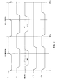
- the circuit diagram shown in FIG. 1 represents a section of a memory level in integrated technology.
- the new read / write amplifier is shown in the lower part of the circuit arrangement. It consists of the two Schottky-clamped transistors T46 and T49 with the Schottky collector contacts S46 and S49.
- the base of transistor T46 is connected to a line WT1 which is common to all read / write amplifiers of a memory level and the base of transistor T49 is connected to a line WTO which is also common to all read / write amplifiers of a memory level .
- the bases of the two transistors T46 and T49 are connected via a common line to a bit selection line BS, which is connected to the base of one bit switch T51 via two Schottky diodes D50 and D51 connected in series.
- This transistor T51 which represents the bit switch for the bit line BL1
- the transistor T50 is connected to the bit line BL1
- the transistor T50 to the bit line BLO
- the other electrode is both connected to a bit reference line BRL at the memory level.
- the bases of both transistors T50 and T51 are supplied with a current via a resistor R50, which is connected to a further reference line BRBL, which keeps these transistors saturated during the idle period.
- word lines WL are present in FIG. 1 for each memory cell CO, 1, ..., of which, however, only the word lines WLO and WL1 for the memory cells CO and C1 are shown in this circuit diagram.
- a known differential amplifier not shown, is connected to the bit lines BLO and BL1 for sensing the stored information and is common to all cells within a bit line pair BLO, BL1.
- the task of the Schottky diodes D50, D51 and the resistor R50 is to prepare and set the rest and operating potentials during the individual memory operations in a known manner.
- the currents for the bit lines BLO and BL1 are supplied via the transistors T50 and T51 serving as bit line switches. These two transistors T50 and T51 are operated inversely and deeply saturated, which ensures that the bit line potentials VBLO and VBL1 differ from each other only by a small amount (typically 3 mV for a stored bit pattern under the most critical conditions).
- the word line potentials VWLO, VWL1, ..., VWL (N-1) are VBE (typically 600 mV) below the bit line potential.
- the memory cell CLO shown in FIG. 1 is to be selected for subsequent reading.
- the bit-side selection of the memory cell CO takes place by pulling down the potential on the line BS (see time diagram according to FIG. 2).
- the two transistors T50 and T51 serving as bit line switches are switched off and the quiescent current is interrupted.
- the memory cell CO in FIG. 1 is selected on the word side by lowering the potential on the word line WLO.
- a charge .DELTA.Q flows in a pulsed manner into the two input capacitances CEOO and CE01, as a result of which the injector voltages of the selected memory cell CO increase. Analyzes in practical tests showed that with a word line swing of recharging the injector capacity with an increase in injector voltages results.
- the discharge currents injected from the injector capacities CEOO and CE01 to the inner cell nodes cause the capacitors CCOO and CC01 to be charged.
- the base-emitter voltage of both NPN transistors T02 and T03 increases.
- the transistor T02 the voltage reaches a value of approximately 400 mV for a short time, starting from approximately 20 mV, after which it drops again very quickly when the base-emitter Capacitance CC01 of transistor T03 is charged to such an extent that the discharge current increases the side of the memory cell CO which is in the off state can be taken over.
- the read signal results from the different degradation of the charges on the side of the memory cell CO that is in the off state and that in the on state.
- the discharge current on the side in the off state is the collector current of the NPN transistor T03 in the on state. This discharge is very quick.
- On the side in the on state corresponds to that of the base current of the NPN transistor T03 in the on state. This is lower than the collector current by the current gain ⁇ u.
- the part of ⁇ Q which is not discharged by the base current remains as a storage charge in the PNP transistor TO1 on the side which is in the on state. This part falls with the storage time constant T S, which is typically 30 ns.
- the larger charge on the side in the on state corresponds to a higher injector voltage.
- one of the two transistors T46 or T49 present in the read / write circuit is activated, i.e. put in the on state.
- the bit line BLO is discharged when the transistor T46 is turned on and the bit line BLO is discharged when the transistor T49 is in the on state.
- the charge Q is formed on the respective input capacitance of the memory cell CO connected to the bit line BLO or BL1, as when reading when the word line potential VWLO is lowered. If, at this point in time, the transistor that was previously in the on state can no longer take over the current flowing into the collector because the PNP transistor integrated with it no longer supplies a base current, the memory cell topples over to the other state, ie The desired binary zero or binary one is entered.
- driver and decoder circuits on the bit and word sides of the memory, respectively, are neither shown nor described because they are well known in the art and are not necessary to explain the present invention.
Abstract
Es wird ein Verfahren zum Lesen und/oder Schreiben eines integrierten Halbleiterspeichers beschrieben, dessen Speicherzellen C aus Flip-Flops mit bipolaren Transistoren bestehen. Der zum Lesen und/oder Schreiben der Speicherzellen C erforderliche Strom wird nur durch die Entladung von Eingangskapazitäten CE der nicht angesteuerten Speicherzellen erzeugt und direkt den angesteuerten Speicherzellen C zugeführt. Dies wird durch eine Schaltungsanordnung erreicht, die zwei Schottky-geklemmte Transistoren T46 und T49 mit Schottky-Kollektorkontakten S46 und S49 aufweist, die mit den Bitleitungen BL0 und BL1 verbunden sind und bei der die Basen der Schottky-geklemmten Transistoren jeweils mit einer Schreib-/Lese-Leitung WT1 bzw. WT0 verbunden sind und die Emitter gemeinsam mit einer Bitselektionsleitung BS.A method for reading and / or writing an integrated semiconductor memory is described, the memory cells C of which consist of flip-flops with bipolar transistors. The current required for reading and / or writing the memory cells C is generated only by the discharge of input capacitances CE of the non-activated memory cells and fed directly to the activated memory cells C. This is achieved by a circuit arrangement which has two Schottky-clamped transistors T46 and T49 with Schottky collector contacts S46 and S49, which are connected to the bit lines BL0 and BL1 and in which the bases of the Schottky-clamped transistors each have a write / Read line WT1 and WT0 are connected and the emitters together with a bit selection line BS.
Description
Die Erfindung betrifft ein Verfahren nach dem Oberbegriff des Patentanspruchs 1 und eine Schaltungsanordnung zur Durchführung des Verfahrens.The invention relates to a method according to the preamble of
Durch die DE-PS 25 11 518 sind ein Verfahren und eine Schaltungsanordnung zum Betreiben eines integrierten Halbleiterspeichers bekannt geworden, dessen Speicherzellen aus Flip-Flops mit bipolaren Transistoren und Schottky-Dioden als Lese-/Schreib-Ankoppelelemente bestehen und die als Lastelemente hochohmige Widerstände oder als Stromquellen geschaltete Transistoren benützen, deren Schreib-/Lesezyklen jeweils in mehreren Phasen ablaufen und die durch Pegeländerungen auf Wortleitungen und Bitleitungen selektiert werden, die zum Erhöhen der Schreib- und Lesegeschwindigkeit sowie zum Verringern der Verlustleistung die'Entladung der Bitleitungen über die leitenden Speicherzellen-Transistoren vornehmen. Die Entladung der Bitleitung über diese leitenden Speicherzellen-Transistoren erfolgt dabei nach Masse. Während der Lesephase des Speichers werden die Bitleitungen nur geringfügig umgeladen, so daß der Umladestrom, der durch die Speicherzelle fließt, dabei sehr klein ist.From DE-PS 25 11 518, a method and a circuit arrangement for operating an integrated semiconductor memory are known, the memory cells of which consist of flip-flops with bipolar transistors and Schottky diodes as read / write coupling elements and which as high-resistance resistors or load elements Use transistors switched as current sources, the write / read cycles of which each run in several phases and which are selected by level changes on word lines and bit lines, which increase the write and read speed and reduce the power loss by discharging the bit lines via the conductive memory cell. Make transistors. The bit line is discharged via these conductive memory cell transistors to ground. During the read phase of the memory, the bit lines are only slightly recharged, so that the recharge current that flows through the memory cell is very small.
In den letzten Jahren hat auf dem Gebiet der logischen Verknüpfungsschaltungen und der integrierten Halbleiterspeichertechnik mit bipolaren Transistoren eine rege Entwicklung stattgefunden, die unter der Bezeichnung MTL (Merged Transistor Logic) oder auch I2L (Integrated Injection Logic) Eingang in die Fachliteratur gefunden hat. Es wird hierzu beispielsweise auf die Aufsätze im IEEE Journal of Solid States Circuits, Band SC/7, Nr. 5, Okt. 1972, Seiten 340 ff. und 346 ff., verwiesen. Entsprechende Vorschläge wurden auch in der US-PS 3 736 477 sowie in der weiteren US-PS 3 816 748 gemacht.In recent years, there has been a lively development in the field of logic logic circuits and integrated semiconductor memory technology with bipolar transistors, which has found its way into the specialist literature under the name MTL (Merged Transistor Logic) or I 2 L (Integrated Injection Logic). For this, reference is made, for example, to the articles in the IEEE Journal of Solid States Circuits, Volume SC / 7, No. 5, Oct. 1972, pages 340 ff. And 346 ff. Appropriate proposals have also been made in U.S. Patent No. 3,736,477 and the other U.S. Patent No. 3,816,748.
Diese Konzepte mit bipolaren Transistoren zeichnen sich durch kurze Schaltzeiten aus und sind zum Aufbau von extrem hochintegrierten Speichern und logischen Schaltungsverbänden besonders geeignet.These concepts with bipolar transistors are characterized by short switching times and are particularly suitable for the construction of extremely highly integrated memories and logic circuit groups.
Speicher, die mit Speicherzellen aus bipolaren Transistoren aufgebaut sind, die eine MTL-ähnliche Struktur aufweisen, verlangen zur Selektion einer Speicherzelle die Umladung von Bitdaten- und/oder Steuerleitungskapazitäten. Der Spannungshub der Bitleitungen entspricht dabei ungefähr dem Spannungshub der selektierten Wortleitungen. Wie bereits in der DE-PS 2 511 518 beschrieben ist, werden die kapazitiven Entladeströme über die Speicherzellen der selektierten Wortleitung und über den Wortleitungstreiber nach Masse abgeführt. Dies hat jedoch bei einer größeren Anzahl von Speicherzellen innerhalb einer Matrix den Nachteil, daß der Flächenbedarf der Treiberschaltkreise, die elektrische Verlustleistung für jeden Treiber und die Verzögerungszeit bei der Selektion der Wortleitung unverhältnismäßig groß wird, so daß die Vorteile der verwendeten MTL-Struktur dadurch wieder zunichte gemacht würden.Memories that are constructed with memory cells made of bipolar transistors that have an MTL-like structure require the reloading of bit data and / or control line capacities in order to select a memory cell. The voltage swing of the bit lines corresponds approximately to the voltage swing of the selected word lines. As already described in DE-PS 2 511 518, the capacitive discharge currents are dissipated to ground via the memory cells of the selected word line and via the word line driver. However, with a larger number of memory cells within a matrix, this has the disadvantage that the area requirement of the driver circuits, the electrical power loss for each driver and the delay time in the selection of the word line become disproportionately large, so that the advantages of the MTL structure used thereby become again would be destroyed.
Um diesen Nachteil zu beseitigen, wurde bereits in der DE-OS 28 55 866 ein Verfahren zum Betreiben eines Halbleiterspeichers und eine Schaltungsanordnung vorgeschlagen, die diese Nachteile nicht mehr aufweisen. Das genannte Verfahren ist dadurch charakterisiert, daß eine an sich bekannte Kontrolle frühzeitig vor dem Selektieren für die Speichermatrix aufgrund eines Auswahlsignales gleichzeitig Steuersignale auf eine Entladeschaltung, die allen Speicherzellen gemeinsam ist, und auf Schalttransistoren abgibt, die daraufhin eingeschaltet werden, daß dadurch auf den Bitdaten- und -steuerleitungen die Entladeströme der Leitungskapazitäten durch die Schalttransistoren fließen und über die Entladeschaltung gemeinsam abfließen. Die genannte Schaltungsanordnung ist dadurch gekennzeichnet, daß die Bitleitungen innerhalb der Speichermatrix mit einer Entladeleitung verbunden sind, die ihrerseits mit einer Entladeschaltung verbunden ist und daß die Entladeschaltung und alle Wort- und/oder Bitleitungsschalttransistoren zur Steuerung über Leitungen mit einer Kontroll- oder Steuerlogik verbunden sind, die mit dem Selektionssignal des Speicherchips gesteuert wird.In order to eliminate this disadvantage, a method for operating a semiconductor memory and a circuit arrangement which no longer have these disadvantages have already been proposed in DE-OS 28 55 866. The above-mentioned method is characterized in that a control known per se emits control signals to a discharge circuit, which is common to all memory cells, and to switching transistors, which are then switched on, by means of a selection signal, early on before selection for the memory matrix Bit data and control lines flow the discharge currents of the line capacitances through the switching transistors and flow off together via the discharge circuit. The circuit arrangement mentioned is characterized in that the bit lines within the memory matrix are connected to a discharge line, which in turn is connected to a discharge circuit, and that the discharge circuit and all word and / or bit line switching transistors for control via lines are connected to a control or control logic , which is controlled with the selection signal of the memory chip.
Obwohl diese Entladeverfahren sowie die Schaltungsanordnungen zur Durchführung dieser Verfahren es gestatten, den minimalen Hub auf der Wortleitung zu verwenden, kapazitive Spitzenströme auf den Spannungsversorgungsleitungen zu verhindern und eine relativ hohe Integration erlauben, haben diese Lösungen folgende Nachteile:
- Der Ablauf der Entladeoperation und der Selektionsoperation der Bitleitungen muß zeitlich nacheinander erfolgen. Der An-w stieg des Abfühlstroms aus dem Abfühlschaltkreis nach der Selektion der Bitleitungen bestimmt mit maßgeblich die Zugriffszeit zur Speicherzelle. Die parallel arbeitenden Bit-und Wortleitungs-Schalttransistoren müssen am Ende der Selektionszeit alle eingeschaltet sein, so daß sich die Zugriffszeit des Speicherchips verlängert.
- The sequence of the discharge operation and the selection operation of the bit lines must take place sequentially. The rise in the sense current from the sense circuit after selection of the bit lines is one of the determining factors in the access time to the memory cell. The bit and word line switching transistors operating in parallel must all be switched on at the end of the selection time, so that the access time of the memory chip is extended.
Die Zahl der erforderlichen Komponenten in den peripheren Schaltkreisen eines solchen Speichers ist jedoch noch sehr hoch. Außerdem ist das gelieferte Lesesignal von dem Gleichstrom abhängig, der von dem Lese-/Schreibverstärker geliefert wird.However, the number of components required in the peripheral circuits of such a memory is still very high. In addition, the read signal supplied is dependent on the direct current supplied by the read / write amplifier.
Der Erfindung liegt deshalb die Aufgabe zugrunde, ein Verfahren zum Lesen und/oder Schreiben eines integrierten Halbleiterspeichers zu schaffen, dessen Speicherzellen insbesondere in MTL-Technik ausgeführt sind, die in Kreuzungspunkten von Wort- und Bitleitungen angeordnet sind und über Treiber und Decodierer selektiert werden, das ein höheres und steileres Lese- und Schreibsignal bei Verringerung der Komponenten in den Lese- und Schreibschaltkreisen und eine Verringerung der erforderlichen Steuerleitungen ermöglicht sowie eine Schaltungsanordnung zur Durchführung des Verfahrens zu schaffen.The invention is therefore based on the object, a Ver drive to read and / or write to create an integrated semiconductor memory, the memory cells are designed in particular in MTL technology, which are arranged at crossing points of word and bit lines and are selected via drivers and decoders, the higher and steeper read and write signal with a reduction in the components in the read and write circuits and a reduction in the required control lines, and to create a circuit arrangement for carrying out the method.
Die erfindungsgemäße Lösung für das Verfahren ergibt sich aus den Kennzeichen der Patentansprüche 1 und 2.The solution according to the invention for the method results from the characteristics of
Eine weitere vorteilhafte Lösung ergibt sich aus dem Kennzeichen des Patentanspruchs 3.A further advantageous solution results from the characterizing part of patent claim 3.
Die erfindungsgemäße Lösung der Schaltungsanordnung ergibt sich aus dem Kennzeichen des Patentanspruchs 4.The solution of the circuit arrangement according to the invention results from the characterizing part of patent claim 4.
Der Vorteil des erfindungsgemäßen Verfahrens besteht in der wesentlichen Verbesserung des Lesesignals, das sich durch eine wesentlich höhere Flankensteilheit und absolute Größe auszeichnet.The advantage of the method according to the invention is the substantial improvement of the read signal, which is characterized by a significantly higher slope and absolute size.
Außerdem wird die Zahl der Komponenten in dem Lese-/Schreibschaltkreis, der jedem Bitleitungspaar zugeordnet ist, wesentlich reduziert, da hier keine Komponenten zur Bereitstellung eines Abfühl- und/oder Schreibgleichstroms mehr erforderlich sind. Die Zahl der Ansteuerleitungen für die Komponenten innerhalb des Lese-/Schreibschaltkreises verringert sich wesentlich. Störende Injektionsströme durch die Isolation zwischen selektierten und nicht selektierten Zellen werden wesentlich reduziert, da der neue Schaltkreis mit niedrigeren Strömen arbeitet. Bezüglich der Spannungspegel auf den Lese-/Schreib- und Bitleitungen ist der neue Lese-/Schreibschaltkreis äußerst unkritisch, da die beiden noch vorhandenen zum Schreiben dienenden Transistoren nie invers einschalten, bedingt dadurch, daß sie durch Schottky-Dioden gesperrt sind.In addition, the number of components in the read / write circuit associated with each pair of bit lines is significantly reduced since no components are required to provide a sense and / or write direct current. The number of drive lines for the components within the read / write circuit is reduced significantly. Interfering injection currents due to the isolation between selected and unselected cells are significantly reduced because the new circuit works with lower currents. Regarding the tension level on the read / write and bit lines, the new read / write circuit is extremely uncritical, since the two transistors still available for writing never turn on inversely, due to the fact that they are blocked by Schottky diodes.
Die Erfindung wird nun anhand eines Ausführungsbeispiels, das in den Zeichnungen dargestellt ist, näher beschrieben.The invention will now be described in more detail using an exemplary embodiment which is illustrated in the drawings.
Es zeigen:
- Fig. 1 einen Ausschnitt aus einer Speicherebene mit dem erfindungsgemäßen Lese-/Schreibschaltkreis;
- Fig. 2 ein Zeitdiagramm für die Lese- und Schreiboperationen, die in der Schaltungsanordnung nach Fig. 1 ablaufen und
- Fig. 3 ein detailliertes Ersatzschaltbild für die Speicherzellen innerhalb einer Kolonne der Speicherebene.
- 1 shows a detail from a memory level with the read / write circuit according to the invention;
- Fig. 2 is a timing diagram for the read and write operations that take place in the circuit arrangement of FIG. 1 and
- Fig. 3 is a detailed equivalent circuit diagram for the memory cells within a column of the storage level.
Das in Fig. 1 gezeigte Schaltbild stellt einen Ausschnitt aus einer Speicherebene in integrierter Technik dar. Im unteren Teil der Schaltungsanordnung ist der neue Lese-/ Schreibverstärker dargestellt. Er besteht aus den beiden Schottky-geklemmten Transistoren T46 und T49 mit den Schottky-Kollektor-Kontakten S46 bzw. S49. Die Basis des Transistors T46 ist mit einer Leitung WT1 verbunden, die für alle Lese-/Schreibverstärker einer Speicherebene gemeinsam vorhanden ist und die Basis des Transistors T49 ist mit einer Leitung WTO verbunden, die für alle Lese-/Schreibverstärker einer Speicherebene ebenfalls gemeinsam vorhanden ist. Die Basen der beiden Transistoren T46 und T49 sind über eine gemeinsame Leitung mit einer Bit-Selektionsleitung BS verbunden, die über zwei in Reihe geschaltete Schottky-Dioden D50 und D51 mit der Basis des einen Bitschalters T51 verbunden ist. Dieser den Bitschalter für die Bitleitung BL1 darstellende Transistor T51 ist mit der Bitleitung BL1 verbunden, der Transistor T50 mit der Bitleitung BLO, während die andere Elektrode beider mit einer Bit-Referenzleitung BRL auf der Speicherebene verbunden ist. Außerdem werden die Basen beider Transistoren T50 und T51 über einen Widerstand R50, der mit einer weiteren Referenzleitung BRBL verbunden ist, mit einem Strom versorgt, der diese Transistoren während der Ruhezeit in Sättigung hält.The circuit diagram shown in FIG. 1 represents a section of a memory level in integrated technology. The new read / write amplifier is shown in the lower part of the circuit arrangement. It consists of the two Schottky-clamped transistors T46 and T49 with the Schottky collector contacts S46 and S49. The base of transistor T46 is connected to a line WT1 which is common to all read / write amplifiers of a memory level and the base of transistor T49 is connected to a line WTO which is also common to all read / write amplifiers of a memory level . The bases of the two transistors T46 and T49 are connected via a common line to a bit selection line BS, which is connected to the base of one bit switch T51 via two Schottky diodes D50 and D51 connected in series. This transistor T51, which represents the bit switch for the bit line BL1, is connected to the bit line BL1, the transistor T50 to the bit line BLO, while the other electrode is both connected to a bit reference line BRL at the memory level. In addition, the bases of both transistors T50 and T51 are supplied with a current via a resistor R50, which is connected to a further reference line BRBL, which keeps these transistors saturated during the idle period.
Im mittleren Teil der Fig. 1 sind zwei Speicherzellen CO und C1 innerhalb des Bitleitungspaares BLO, BL1 dargestellt. Die angedeuteten waagerecht verlaufenden Leitungen oberhalb der Speicherzelle C1 sollen nur andeuten, daß innerhalb dieses Bitleitungspaares BLO, BL1 in der Praxis N Speicherzellen angeordnet sind.In the middle part of FIG. 1, two memory cells CO and C1 are shown within the bit line pair BLO, BL1. The indicated horizontal lines above the memory cell C1 are only intended to indicate that, in practice, N memory cells are arranged within this bit line pair BLO, BL1.
Außerdem sind in der Fig. 1 für jede Speicherzelle CO, 1,... Wortleitungen WL vorhanden, wovon in diesem Schaltbild jedoch nur die Wortleitungen WLO und WL1 für die Speicherzellen CO und C1 dargestellt sind. Außerdem soll noch erwähnt sein, daß an die Bitleitungen BLO und BL1 zum Abfühlen der gespeicherten Informationen ein nicht dargestellter bekannter Differenzverstärker angeschlossen ist, der für alle Zellen innerhalb eines Bitleitungspaares BLO, BL1 gemeinsam ist. Die Aufgabe der Schottky-Dioden D50, D51 und des Widerstands R50 bestehen in der Bereit- und Einstellung der Ruhe- und Betriebspotentiale während der einzelnen Speicheroperationen auf bekannte Art und Weise.In addition, word lines WL are present in FIG. 1 for each memory cell CO, 1, ..., of which, however, only the word lines WLO and WL1 for the memory cells CO and C1 are shown in this circuit diagram. It should also be mentioned that a known differential amplifier, not shown, is connected to the bit lines BLO and BL1 for sensing the stored information and is common to all cells within a bit line pair BLO, BL1. The task of the Schottky diodes D50, D51 and the resistor R50 is to prepare and set the rest and operating potentials during the individual memory operations in a known manner.
Im folgenden sei nun anhand des in Fig. 2 gezeigten Zeitdiagramms für je einen Lese- und Schreibzyklus, in der Figur als R-Operation bzw. WR-Operation gekennzeichnet, die Wirkungsweise des in Fig. 1 gezeigten Schaltbildes näher erklärt.The following is now based on the time diagram shown in FIG. 2 for one read and one write cycle in the figure characterized as an R operation or WR operation, the mode of operation of the circuit diagram shown in Fig. 1 explained in more detail.
Zunächst wird angenommen, daß sich der Speicher im Ruhezustand befindet, d.h., daß alle Potentiale und Ströme sich so eingestellt haben, daß nur ein sehr kleiner Leistungsverlust auftritt. Die Ströme für die Bitleitungen BLO und BL1 werden über die als Bitleitungsschalter dienenden Transistoren T50 und T51 geliefert. Diese beiden Transistoren T50 und T51 sind invers betrieben und tief gesättigt, wodurch gewährleistet ist, daß sich die Bitleitungspotentiale VBLO und VBL1 nur um einen geringen Betrag voneinander unterscheiden (typisch 3 mV für ein eingespeichertes Bitmuster unter kritischsten Bedingungen). Die Wortleitungspotentiale VWLO, VWL1, ..., VWL(N-1) liegen um VBE (typisch 600 mV) unter dem Bitleitungspotential.First, it is assumed that the memory is at rest, i.e. that all potentials and currents have been set so that there is only a very small loss of power. The currents for the bit lines BLO and BL1 are supplied via the transistors T50 and T51 serving as bit line switches. These two transistors T50 and T51 are operated inversely and deeply saturated, which ensures that the bit line potentials VBLO and VBL1 differ from each other only by a small amount (typically 3 mV for a stored bit pattern under the most critical conditions). The word line potentials VWLO, VWL1, ..., VWL (N-1) are VBE (typically 600 mV) below the bit line potential.
Im folgenden soll nun angenommen werden, daß die in Fig. 1 dargestellte Speicherzelle CLO zum nachfolgenden Lesen selektiert werden soll. Die bitseitige Selektion der Speicherzelle CO erfolgt durch Herabziehen des Potentials auf der Leitung BS (siehe Zeitdiagramm nach Fig. 2). Dadurch werden die beiden als Bitleitungsschalter dienenden Transistoren T50 und T51 abgeschaltet und der Ruhestrom wird unterbrochen. Die Selektion der Speicherzelle CO in Fig. 1 auf der Wortseite erfolgt durch Absenken des Potentials auf der Wortleitung WLO.In the following, it should now be assumed that the memory cell CLO shown in FIG. 1 is to be selected for subsequent reading. The bit-side selection of the memory cell CO takes place by pulling down the potential on the line BS (see time diagram according to FIG. 2). As a result, the two transistors T50 and T51 serving as bit line switches are switched off and the quiescent current is interrupted. The memory cell CO in FIG. 1 is selected on the word side by lowering the potential on the word line WLO.
Wenn nun das Potential auf der Wortleitung WLO sprungartig herabgezogen wird, bilden die Parallelschaltungen der Injektorkapazitäten der nicht-selektierten Zellen und der Bitleitungs-Metall-Kapazitäten CSO und CS1.![]()
![]()
![]()
![]()
In die beiden Eingangskapazitäten CEOO und CE01 fließt impulsförmig eine Ladung ΔQ, wodurch sich die Injektorspannungen der selektierten Speicherzelle CO erhöhen. Analysen bei praktischen Versuchen ergaben, daß sich bei einem Wortleitungshub von![]()
![]()
![]()
![]()
![]()
![]()
Die in die Injektoren fließenden LadungenAQ entsprechen über den Taktzyklus tCL = 50 ns gemittelt, einem mittleren Lesestrom von IO = I1 =Δ Q/tCL (≈20 µA).The charges AQ flowing into the injectors correspond to averaged over the clock cycle tCL = 50 ns, an average reading current of IO = I1 = Δ Q / tCL (≈20 µA).
Der Ausgleichsvorgang für ΔQ nach dem Herabziehen des Potentials auf der Wortleitung, z.B. WLO, ist äußerst komplex und wird anschließend anhand der Fig. 3 näher erklärt.The equalization process for ΔQ after pulling down the potential on the word line, e.g. WLO is extremely complex and is subsequently explained in more detail with reference to FIG. 3.
Anfangs bewirken die von den Injektorkapazitäten CEOO und CE01 zu den inneren Zellknoten injizierten Entladungsströme eine Aufladung der dargestellten Kapazitäten CCOO und CC01. Dabei steigt die Basis-Emitterspannung beider NPN-Transistoren T02 und T03 an. Auf der sich im Aus-Zustand befindlichen Seite der Speicherzelle CO, hier der Transistor T02, erreicht die Spannung, ausgehend von ca. 20 mV kurzzeitig einen Wert von ca. 400 mV, worauf sie sehr rasch wieder abfällt, wenn die Basis-Emitter-Kapazität CC01 des Transistors T03 so weit aufgeladen ist, daß der Entladestrom auf der sich im Aus-Zustand befindlichen Seite der Speicherzelle CO übernommen werden kann.Initially, the discharge currents injected from the injector capacities CEOO and CE01 to the inner cell nodes cause the capacitors CCOO and CC01 to be charged. The base-emitter voltage of both NPN transistors T02 and T03 increases. On the side of the memory cell CO that is in the off state, here the transistor T02, the voltage reaches a value of approximately 400 mV for a short time, starting from approximately 20 mV, after which it drops again very quickly when the base-emitter Capacitance CC01 of transistor T03 is charged to such an extent that the discharge current increases the side of the memory cell CO which is in the off state can be taken over.
Auf der sich im Ein-Zustand befindlichen Seite, d.h., in Fig. 3 am Transistor T03, steigt die Spannung von ca. 600 mV auf ca. 800 mV, um dann langsam wieder abzufallen.On the side in the on-state, i.e., in Fig. 3 at transistor T03, the voltage rises from approx. 600 mV to approx. 800 mV and then slowly drops again.
Das Lesesignal ergibt sich aus dem unterschiedlichen Abbau der Ladungen der sich im Aus-Zustand und der sich im Ein- Zustand befindlichen Seite der Speicherzelle CO. Der Entladestrom auf der sich im Aus-Zustand befindlichen Seite ist der Kollektorstrom des sich im Ein-Zustand befindlichen NPN-Transistors T03. Diese Entladung verläuft sehr rasch. Auf der sich im Ein-Zustand befindlichen Seite entspricht dem der Basisstrom des sich im Ein-Zustand befindlichen NPN-Transistors T03. Dieser ist um die Stromverstärkung βu niedriger als der Kollektorstrom. Der durch den Basisstrom nicht entladene Teil von ΔQ verbleibt als Speicherladung im PNP-Transistor TO1 auf der sich im Ein-Zustand befindlichen Seite. Dieser Teil fällt mit der Speicherzeitkonstanten TS, die typischerweise bei 30 ns liegt, ab. Der größeren Ladung auf der sich im Ein-Zustand befindlichen Seite entspricht eine höhere Injektorspannung.The read signal results from the different degradation of the charges on the side of the memory cell CO that is in the off state and that in the on state. The discharge current on the side in the off state is the collector current of the NPN transistor T03 in the on state. This discharge is very quick. On the side in the on state corresponds to that of the base current of the NPN transistor T03 in the on state. This is lower than the collector current by the current gain βu. The part of ΔQ which is not discharged by the base current remains as a storage charge in the PNP transistor TO1 on the side which is in the on state. This part falls with the storage time constant T S, which is typically 30 ns. The larger charge on the side in the on state corresponds to a higher injector voltage.
Somit ist gezeigt worden, daß lediglich durch die kapazitiven Ströme auf den Bitleitungen BLO und BL1, d.h. ohne jegliche zusätzlich generierte Ströme durch die Lese-/Schreibschaltung das Lesen der gespeicherten Information in der Speicherzelle CO möglich ist.Thus, it has been shown that only by the capacitive currents on bit lines BLO and BL1, i.e. it is possible to read the stored information in the memory cell CO without any additional currents generated by the read / write circuit.
In Fig. 3 sind außerdem der Vollständigkeit halber noch die Ersatzkomponenten der Speicherzellen C1 und C2 angedeutet. Im nachfolgenden soll noch kurz auf die Schreiboperation und die dabei auftretenden Ströme eingegangen werden.For the sake of completeness, the replacement components of the memory cells C1 and C2 are also indicated in FIG. 3. In the following, the write operation and the currents that occur will be briefly discussed.
Zum Schreiben wird einer der beiden im Lese-/Schreibschaltkreis vorhandenen Transistoren T46 bzw. T49 aktiviert, d.h. in den Ein-Zustand versetzt. Mit anderen Worten, die Bitleitung BLO wird entladen, wenn der Transistor T46 eingeschaltet wird und die Bitleitung BLO wird entladen, wenn sich der Transistor T49 im Ein-Zustand befindet. An der jeweiligen, mit der Bitleitung BLO oder BL1 verbundenen Eingangskapazität der Speicherzelle CO bildet sich, wie beim Lesen bei Absenkung des Wortleiungspotentials VWLO, die Ladung Q aus. Wenn zu diesem Zeitpunkt, der sich bisher im Ein-Zustand befindliche Transistor den in den Kollektor fließenden Strom nicht mehr übernehmen kann, weil der mit ihm integrierte PNP-Transistor keinen Basisstrom mehr liefert, kippt die Speicherzelle in den anderen Zustand um, d.h., die gewünschte binäre Null, bzw. binäre Eins ist eingeschrieben.For writing, one of the two transistors T46 or T49 present in the read / write circuit is activated, i.e. put in the on state. In other words, the bit line BLO is discharged when the transistor T46 is turned on and the bit line BLO is discharged when the transistor T49 is in the on state. The charge Q is formed on the respective input capacitance of the memory cell CO connected to the bit line BLO or BL1, as when reading when the word line potential VWLO is lowered. If, at this point in time, the transistor that was previously in the on state can no longer take over the current flowing into the collector because the PNP transistor integrated with it no longer supplies a base current, the memory cell topples over to the other state, ie The desired binary zero or binary one is entered.
Auch hier wurde klar gezeigt, daß außer den kapazitiven Strömen zum Schreiben einer Information in den Speicher keine weiteren Ströme erforderlich sind und gerade deshalb ein sehr schnelles und sauberes Schalten möglich ist. Aus dem Schaltbild nach Fig. 1 geht auch klar hervor, daß der technische Aufwand für den Lese-/Schreibschaltkreis bei der Verwendung nur kapazitiver Ströme zum Lesen und/oder Schreiben von Informationen äußerst gering ist. Ein weiterer Vorteil besteht darin, daß wenig Steuerleitungen erforderlich sind, so daß eine sehr hohe Integrationsdichte erzielbar ist.Here, too, it was clearly shown that, apart from the capacitive currents for writing information into the memory, no further currents are required and precisely for this reason very fast and clean switching is possible. 1 clearly shows that the technical outlay for the read / write circuit when using only capacitive currents for reading and / or writing information is extremely low. Another advantage is that few control lines are required, so that a very high integration density can be achieved.
Die Treiberschaltungen und Decodierschaltungen auf der Bit- bzw. auf der Wortseite des Speichers sind weder dargestellt noch werden sie beschrieben, weil sie in der Technik hinlänglich bekannt sind und zur Erklärung der vorliegenden Erfindung nicht erforderlich sind.The driver and decoder circuits on the bit and word sides of the memory, respectively, are neither shown nor described because they are well known in the art and are not necessary to explain the present invention.
Claims (4)
Applications Claiming Priority (2)
| Application Number | Priority Date | Filing Date | Title |
|---|---|---|---|
| DE2926050 | 1979-06-28 | ||
| DE2926050A DE2926050C2 (en) | 1979-06-28 | 1979-06-28 | Method and circuit arrangement for reading and / or writing an integrated semiconductor memory with memory cells using MTL technology |
Publications (2)
| Publication Number | Publication Date |
|---|---|
| EP0020995A1 true EP0020995A1 (en) | 1981-01-07 |
| EP0020995B1 EP0020995B1 (en) | 1983-06-15 |
Family
ID=6074350
Family Applications (1)
| Application Number | Title | Priority Date | Filing Date |
|---|---|---|---|
| EP80102653A Expired EP0020995B1 (en) | 1979-06-28 | 1980-05-13 | Method and circuit for selection and for discharging bit line capacitances of a highly integrated mtl semiconductor memory |
Country Status (5)
| Country | Link |
|---|---|
| US (1) | US4330853A (en) |
| EP (1) | EP0020995B1 (en) |
| JP (1) | JPS5824875B2 (en) |
| DE (2) | DE2926050C2 (en) |
| IT (1) | IT1174672B (en) |
Cited By (3)
| Publication number | Priority date | Publication date | Assignee | Title |
|---|---|---|---|---|
| EP0031462A2 (en) * | 1979-12-27 | 1981-07-08 | International Business Machines Corporation | Differential charge sensing system for a four device MTL memory cell |
| EP0069227A2 (en) * | 1981-07-06 | 1983-01-12 | International Business Machines Corporation | Integrated semiconductor memory and method for accessing and reading |
| EP0078335A1 (en) * | 1981-10-30 | 1983-05-11 | Ibm Deutschland Gmbh | Method for reading a semiconductor memory |
Families Citing this family (8)
| Publication number | Priority date | Publication date | Assignee | Title |
|---|---|---|---|---|
| US4601016A (en) * | 1983-06-24 | 1986-07-15 | Honeywell Inc. | Semiconductor memory cell |
| US4598390A (en) * | 1984-06-25 | 1986-07-01 | International Business Machines Corporation | Random access memory RAM employing complementary transistor switch (CTS) memory cells |
| US4596002A (en) * | 1984-06-25 | 1986-06-17 | International Business Machines Corporation | Random access memory RAM employing complementary transistor switch (CTS) memory cells |
| US4578779A (en) * | 1984-06-25 | 1986-03-25 | International Business Machines Corporation | Voltage mode operation scheme for bipolar arrays |
| US4752913A (en) * | 1986-04-30 | 1988-06-21 | International Business Machines Corporation | Random access memory employing complementary transistor switch (CTS) memory cells |
| EP0246371B1 (en) * | 1986-05-22 | 1991-01-09 | International Business Machines Corporation | Integrated injection logic output circuit |
| US4763026A (en) * | 1987-04-09 | 1988-08-09 | National Semiconductor Corporation | Sense amplifier for single-ended data sensing |
| US5526319A (en) * | 1995-01-31 | 1996-06-11 | International Business Machines Corporation | Memory with adiabatically switched bit lines |
Citations (11)
| Publication number | Priority date | Publication date | Assignee | Title |
|---|---|---|---|---|
| US3540010A (en) * | 1968-08-27 | 1970-11-10 | Bell Telephone Labor Inc | Diode-coupled semiconductive memory |
| US3541531A (en) * | 1967-02-07 | 1970-11-17 | Bell Telephone Labor Inc | Semiconductive memory array wherein operating power is supplied via information paths |
| US3688264A (en) * | 1970-09-18 | 1972-08-29 | Rca Corp | Operation of field-effect transistor circuits having substantial distributed capacitance |
| US3736574A (en) * | 1971-12-30 | 1973-05-29 | Ibm | Pseudo-hierarchy memory system |
| US3786442A (en) * | 1972-02-24 | 1974-01-15 | Cogar Corp | Rapid recovery circuit for capacitively loaded bit lines |
| US3900838A (en) * | 1973-02-27 | 1975-08-19 | Ibm | Hybrid storage circuit |
| US4070656A (en) * | 1975-12-17 | 1978-01-24 | International Business Machines Corporation | Read/write speed up circuit for integrated data memories |
| US4090255A (en) * | 1975-03-15 | 1978-05-16 | International Business Machines Corporation | Circuit arrangement for operating a semiconductor memory system |
| US4112511A (en) * | 1977-09-13 | 1978-09-05 | Signetics Corporation | Four transistor static bipolar memory cell using merged transistors |
| EP0004871A1 (en) * | 1978-04-19 | 1979-10-31 | International Business Machines Corporation | Monolithic integrated semiconductor device with at least one I2L structure, memory cell using such device and memory matrix using such memory cell |
| EP0013302A1 (en) * | 1978-12-22 | 1980-07-23 | International Business Machines Corporation | Process and circuitry for operating an integrated semi-conductor memory |
Family Cites Families (12)
| Publication number | Priority date | Publication date | Assignee | Title |
|---|---|---|---|---|
| US3815106A (en) * | 1972-05-11 | 1974-06-04 | S Wiedmann | Flip-flop memory cell arrangement |
| US3668264A (en) * | 1969-07-15 | 1972-06-06 | Union Oil Co | Production of alkylbenzenes |
| US3643231A (en) * | 1970-04-20 | 1972-02-15 | Ibm | Monolithic associative memory cell |
| DE2021824C3 (en) * | 1970-05-05 | 1980-08-14 | Ibm Deutschland Gmbh, 7000 Stuttgart | Monolithic semiconductor circuit |
| US3816758A (en) * | 1971-04-14 | 1974-06-11 | Ibm | Digital logic circuit |
| US3816748A (en) * | 1972-04-28 | 1974-06-11 | Alpha Ind Inc | Ion accelerator employing crossed-field selector |
| US3786422A (en) * | 1973-01-31 | 1974-01-15 | Rel Reeves Inc | System for determination of deviations of a vehicle from a prescribed route |
| US3866531A (en) * | 1973-10-12 | 1975-02-18 | Sperry Rand Corp | Apparatus for controlling the movement of crop material in a roll forming machine |
| GB1494481A (en) * | 1973-12-21 | 1977-12-07 | Mullard Ltd | Electrical circuits comprising master/slave bistable arrangements |
| US4021786A (en) * | 1975-10-30 | 1977-05-03 | Fairchild Camera And Instrument Corporation | Memory cell circuit and semiconductor structure therefore |
| US4032902A (en) * | 1975-10-30 | 1977-06-28 | Fairchild Camera And Instrument Corporation | An improved semiconductor memory cell circuit and structure |
| JPS53117341A (en) * | 1977-03-24 | 1978-10-13 | Toshiba Corp | Semiconductor memory |
-
1979
- 1979-06-28 DE DE2926050A patent/DE2926050C2/en not_active Expired
-
1980
- 1980-04-03 US US06/136,859 patent/US4330853A/en not_active Expired - Lifetime
- 1980-05-09 JP JP55060778A patent/JPS5824875B2/en not_active Expired
- 1980-05-13 DE DE8080102653T patent/DE3063756D1/en not_active Expired
- 1980-05-13 EP EP80102653A patent/EP0020995B1/en not_active Expired
- 1980-06-06 IT IT22604/80A patent/IT1174672B/en active
Patent Citations (11)
| Publication number | Priority date | Publication date | Assignee | Title |
|---|---|---|---|---|
| US3541531A (en) * | 1967-02-07 | 1970-11-17 | Bell Telephone Labor Inc | Semiconductive memory array wherein operating power is supplied via information paths |
| US3540010A (en) * | 1968-08-27 | 1970-11-10 | Bell Telephone Labor Inc | Diode-coupled semiconductive memory |
| US3688264A (en) * | 1970-09-18 | 1972-08-29 | Rca Corp | Operation of field-effect transistor circuits having substantial distributed capacitance |
| US3736574A (en) * | 1971-12-30 | 1973-05-29 | Ibm | Pseudo-hierarchy memory system |
| US3786442A (en) * | 1972-02-24 | 1974-01-15 | Cogar Corp | Rapid recovery circuit for capacitively loaded bit lines |
| US3900838A (en) * | 1973-02-27 | 1975-08-19 | Ibm | Hybrid storage circuit |
| US4090255A (en) * | 1975-03-15 | 1978-05-16 | International Business Machines Corporation | Circuit arrangement for operating a semiconductor memory system |
| US4070656A (en) * | 1975-12-17 | 1978-01-24 | International Business Machines Corporation | Read/write speed up circuit for integrated data memories |
| US4112511A (en) * | 1977-09-13 | 1978-09-05 | Signetics Corporation | Four transistor static bipolar memory cell using merged transistors |
| EP0004871A1 (en) * | 1978-04-19 | 1979-10-31 | International Business Machines Corporation | Monolithic integrated semiconductor device with at least one I2L structure, memory cell using such device and memory matrix using such memory cell |
| EP0013302A1 (en) * | 1978-12-22 | 1980-07-23 | International Business Machines Corporation | Process and circuitry for operating an integrated semi-conductor memory |
Non-Patent Citations (6)
| Title |
|---|
| ELECTRONICS, Band 47, Nr. 9, 2. Mai 1974, Seiten 110-114 New York, U.S.A. GERSBACH: "Current Steering Simplifies and Shrinks 1k Bipolar RAM" * Seiten 112-114, Abschnitt: "A slightly different bit drive"; Figuren 1, 3, 4 * & US - A - 3 736 574 (I.B.M.). * |
| I.B.M. TECHNICAL DISCLOSURE BULLETIN, Band 21, Nr. 1, Juni 1978, Seiten 231-232 Armonk, U.S.A. WIEDMANN: "MTL Storage Cell". * |
| IBM TECHNICAL DISCLOSURE BULLETIN, Band 13, Nr. 6, November 1970, Seiten 1705-1706 Armonk, U.S.A. WIEDMANN et al.: "Restore Circuitry for Bit/Sense System" * Seiten 1705-1706 * * |
| IEEE JOURNAL OF SOLID-STATE CIRCUITS, Band SC13, Nr. 5, Oktober 1978, Seiten 656-663 New York, U.S.A. KAWARADA et al.: "A Fast 7.5 ns Access 1K-Bit RAM for Cache-Memory Systems" * Seiten 659-660, Abschnitt: "F. Error-Write Suppression and Bit Line Clamping"; Figuren 5-9 * * |
| IEEE JOURNAL OF SOLID-STATE CIRCUITS, Band SC2, Nr. 4, Dezember 1967, Seiten 196-201 New York, U.S.A. IWERSEN: "Beam-Lead Sealed-Junction Semiconductor Memory with Minimal Cell Complexity" & US - A - 3 541 531 (BELL). * |
| IEEE JOURNAL OF SOLID-STATE CIRCUITS, Band SC6, Nr. 5, Oktober 1971, Seiten 297-300 New York, U.S.A. HENN: "Bipolar Dynamic Memory Cell". * |
Cited By (5)
| Publication number | Priority date | Publication date | Assignee | Title |
|---|---|---|---|---|
| EP0031462A2 (en) * | 1979-12-27 | 1981-07-08 | International Business Machines Corporation | Differential charge sensing system for a four device MTL memory cell |
| EP0031462A3 (en) * | 1979-12-27 | 1981-08-05 | International Business Machines Corporation | Differential charge sensing system for an integrated memory using dual-capacitance cells coupled to two bit lines |
| EP0069227A2 (en) * | 1981-07-06 | 1983-01-12 | International Business Machines Corporation | Integrated semiconductor memory and method for accessing and reading |
| EP0069227A3 (en) * | 1981-07-06 | 1985-04-03 | International Business Machines Corporation | Integrated semiconductor memory and method for accessing and reading |
| EP0078335A1 (en) * | 1981-10-30 | 1983-05-11 | Ibm Deutschland Gmbh | Method for reading a semiconductor memory |
Also Published As
| Publication number | Publication date |
|---|---|
| US4330853A (en) | 1982-05-18 |
| DE3063756D1 (en) | 1983-07-21 |
| DE2926050C2 (en) | 1981-10-01 |
| IT8022604A0 (en) | 1980-06-06 |
| JPS5824875B2 (en) | 1983-05-24 |
| IT1174672B (en) | 1987-07-01 |
| JPS567291A (en) | 1981-01-24 |
| EP0020995B1 (en) | 1983-06-15 |
| DE2926050B1 (en) | 1981-01-08 |
Similar Documents
| Publication | Publication Date | Title |
|---|---|---|
| DE2659248C3 (en) | Dynamic memory with random access | |
| DE2556831C2 (en) | Matrix memory and procedure for its operation | |
| DE1499843B2 (en) | Arrangement with at least one memory cell with a plurality of transistors | |
| DE2707456C3 (en) | ||
| EP0020995B1 (en) | Method and circuit for selection and for discharging bit line capacitances of a highly integrated mtl semiconductor memory | |
| EP0013302B1 (en) | Process and circuitry for operating an integrated semi-conductor memory | |
| DE2429771A1 (en) | STORAGE MATRIX WITH CONTROLLABLE FOUR-LAYER SEMI-CONDUCTORS | |
| DE3038641A1 (en) | SEMICONDUCTOR MEMORY CIRCUIT | |
| DE2302137B2 (en) | Reading circuit for non-destructive reading of dynamic charge storage cells | |
| EP0078335B1 (en) | Method for reading a semiconductor memory | |
| DE3305427C2 (en) | Bipolar semiconductor memory | |
| EP0021143B1 (en) | Method and circuit for selection and for discharging bit lines capacitances in a highly integrated semi-conductor memory | |
| EP0031001B1 (en) | Method for capacitive read-signal amplification in an integrated semiconductor memory with mtl technique memory cells | |
| DE2152706B2 (en) | MONOLITHIC INTEGRATED SEMI-CONDUCTOR MEMORY FOR BINARY DATA | |
| EP0022930B1 (en) | Recharge circuit for a semi-conductor memory | |
| DE2556833B2 (en) | Method and circuit arrangement for operating a semiconductor memory | |
| EP0003030A2 (en) | Bipolar dynamic memory cell | |
| DE3938638A1 (en) | SEMICONDUCTOR MEMORY DEVICE WITH AN IMPROVED CURRENT TYPE READING AMPLIFIER AND METHOD FOR OPERATING THE SAME | |
| DE1774948C3 (en) | Word organized memory. Eliminated from: 1499843 | |
| DE1499843C (en) | Arrangement with at least one storage cell with several transistors | |
| DE2348065C3 (en) | Bipolar transistor memory with capacitive storage | |
| DE2002708C3 (en) | Memory arrangement with bistable flip-flops | |
| DE2511518C3 (en) | Method and circuit arrangement for operating a semiconductor memory | |
| DE1499857C (en) | Read driver circuit for a data memory | |
| DE2654460A1 (en) | CIRCUIT TO INCREASE THE WRITING SPEED FOR MEMORY CELLS |
Legal Events
| Date | Code | Title | Description |
|---|---|---|---|
| PUAI | Public reference made under article 153(3) epc to a published international application that has entered the european phase |
Free format text: ORIGINAL CODE: 0009012 |
|
| AK | Designated contracting states |
Designated state(s): DE FR GB NL SE |
|
| 17P | Request for examination filed |
Effective date: 19810312 |
|
| GRAA | (expected) grant |
Free format text: ORIGINAL CODE: 0009210 |
|
| AK | Designated contracting states |
Designated state(s): DE FR GB NL SE |
|
| PG25 | Lapsed in a contracting state [announced via postgrant information from national office to epo] |
Ref country code: NL Effective date: 19830615 |
|
| REF | Corresponds to: |
Ref document number: 3063756 Country of ref document: DE Date of ref document: 19830721 |
|
| ET | Fr: translation filed | ||
| NLV1 | Nl: lapsed or annulled due to failure to fulfill the requirements of art. 29p and 29m of the patents act | ||
| PLBE | No opposition filed within time limit |
Free format text: ORIGINAL CODE: 0009261 |
|
| STAA | Information on the status of an ep patent application or granted ep patent |
Free format text: STATUS: NO OPPOSITION FILED WITHIN TIME LIMIT |
|
| PGFP | Annual fee paid to national office [announced via postgrant information from national office to epo] |
Ref country code: SE Payment date: 19840630 Year of fee payment: 5 |
|
| 26N | No opposition filed | ||
| PG25 | Lapsed in a contracting state [announced via postgrant information from national office to epo] |
Ref country code: SE Effective date: 19860514 |
|
| PGFP | Annual fee paid to national office [announced via postgrant information from national office to epo] |
Ref country code: GB Payment date: 19900404 Year of fee payment: 11 |
|
| PGFP | Annual fee paid to national office [announced via postgrant information from national office to epo] |
Ref country code: DE Payment date: 19900529 Year of fee payment: 11 |
|
| PGFP | Annual fee paid to national office [announced via postgrant information from national office to epo] |
Ref country code: FR Payment date: 19910430 Year of fee payment: 12 |
|
| PG25 | Lapsed in a contracting state [announced via postgrant information from national office to epo] |
Ref country code: GB Effective date: 19910513 |
|
| GBPC | Gb: european patent ceased through non-payment of renewal fee | ||
| PG25 | Lapsed in a contracting state [announced via postgrant information from national office to epo] |
Ref country code: DE Effective date: 19920303 |
|
| PG25 | Lapsed in a contracting state [announced via postgrant information from national office to epo] |
Ref country code: FR Effective date: 19930129 |
|
| REG | Reference to a national code |
Ref country code: FR Ref legal event code: ST |
|
| EUG | Se: european patent has lapsed |
Ref document number: 80102653.5 Effective date: 19870225 |