EP0028774A2 - Apparatus for detecting defects in a periodic pattern - Google Patents
Apparatus for detecting defects in a periodic pattern Download PDFInfo
- Publication number
- EP0028774A2 EP0028774A2 EP80106681A EP80106681A EP0028774A2 EP 0028774 A2 EP0028774 A2 EP 0028774A2 EP 80106681 A EP80106681 A EP 80106681A EP 80106681 A EP80106681 A EP 80106681A EP 0028774 A2 EP0028774 A2 EP 0028774A2
- Authority
- EP
- European Patent Office
- Prior art keywords
- light
- periodic pattern
- order diffraction
- pattern
- defect
- Prior art date
- Legal status (The legal status is an assumption and is not a legal conclusion. Google has not performed a legal analysis and makes no representation as to the accuracy of the status listed.)
- Granted
Links
Images


Classifications
-
- G—PHYSICS
- G01—MEASURING; TESTING
- G01N—INVESTIGATING OR ANALYSING MATERIALS BY DETERMINING THEIR CHEMICAL OR PHYSICAL PROPERTIES
- G01N21/00—Investigating or analysing materials by the use of optical means, i.e. using sub-millimetre waves, infrared, visible or ultraviolet light
- G01N21/84—Systems specially adapted for particular applications
- G01N21/88—Investigating the presence of flaws or contamination
- G01N21/95—Investigating the presence of flaws or contamination characterised by the material or shape of the object to be examined
- G01N21/956—Inspecting patterns on the surface of objects
- G01N21/95623—Inspecting patterns on the surface of objects using a spatial filtering method
-
- G—PHYSICS
- G02—OPTICS
- G02B—OPTICAL ELEMENTS, SYSTEMS OR APPARATUS
- G02B27/00—Optical systems or apparatus not provided for by any of the groups G02B1/00 - G02B26/00, G02B30/00
- G02B27/42—Diffraction optics, i.e. systems including a diffractive element being designed for providing a diffractive effect
- G02B27/46—Systems using spatial filters
Definitions
- the present invention relates to an apparatus for inspecting defects in a periodic pattern.
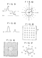
- a mesh plate with a number of periodic square holes may have one kind of defect which is an enlarged hole as shown in Fig. 1A and another kind of defect which is a reduced hole as shown in Fig. 1B.
- E is light information from the examined mesh plate pattern
- P light information from an ideal periodic pattern
- D light information representing defects.
- the mesh plate with a reduced hole shown Fig. 1B can be repaired by manually removing the intruding part 10 to thereby improve the yield. Also, there is sometimes a difference in the acceptable tolerance between an enlarged hole and a reduced hole.
- an apparatus for inspecting defects in a periodic pattern includes a device for forming a Fourier transformed pattern of the periodic pattern.
- a filter is then provided for passing predetermined spatial frequency ranges of the Fourier transformed pattern, the predetermined spatial frequency ranges being lower than a spatial frequency which coincides with a first order diffraction of the Fourier transformed pattern.
- defect means any factor which distorts a periodic pattern such as a different size pattern, deformation of the pattern, scratches on the pattern, dust stack to the pattern, etc.
- the defect inspection-apparatus according to the invention is used to detect such defects in the periodic pattern.
- a mesh plate with a mesh pattern generally is formed in a vidicon or shadow mask of a color cathode ray tube for use as an object to be inspected.
- Such an object is not limited to a mesh plate but may be an opaque object with a periodic pattern, for example, such as used in semiconductor products.
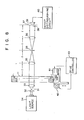
- a mesh plate 11 is shown with a number of periodically arranged square holes 12. As shown in Figs. 2 and 3, the mesh plate 11 is illuminated by a coherent light beam 13.
- a lens 14, a spatial filter 15, and a lens 16 are positioned in order on an optical path 17 of the beam 13, the spatial filter 15 being positioned at the focal point of lenses 14 and 16.
- Lens 14 forms a spatial Fourier transformer and lens 16 forms the inverse spatial Fourier transformer.
- a zeroth order diffraction light component is directed to the origin to form a zeroth order spot 20 and a first order diffraction light components are directed to outside of the zeroth order spot 20 to form a first order spot 21.
- second and higher order diffraction light components are similarly directed to further outside of the preceding order diffraction spots.
- the light intensity distribution of these diffraction light components on the axis of Fig. 4 is generally illustrated by a solid line A in Fig. 5.
- the spot size of each diffracted light component indicates approximately the relative light intensity level.
- the size of the diffraction areas and the distance between the diffraction areas is as follows.
- P denotes the pitch of the mesh pattern 18, i.e., the interval between the adjacent holes 12
- the diameter of zeroth order diffraction area 20 is and the distance between zeroth order diffraction area 20 and first order diffraction area 21 is , where X is the wavelength of the coherent light projected and f is the focal length of the lens.
- the diffraction pattern as shown in Figs. 4 and 5 is periodic and is determined by the hole pattern in mesh plate 11. If a hole 12 has a defect as shown Fig. lA, the defect diffracted pattern is given by a dotted line B in Fig. 5. Therefore, if a spatial filter is used to filter out the periodic diffraction pattern, e.g., a spatial filter 22 having a ring-like transmission area 23 as shown in Fig. 6, the non-periodic pattern represents the defect, namely, only the defect information may be extracted from the diffracted pattern in Fig. 4. For example, if spatial filter 22 is placed at back focal plane of lens 14 shown in Fig. 3, a mesh pattern having only defect information light is obtained at the back focal plane of lens 16.
- the primary feature of the present invention is to extract not only the non-periodic pattern information component but also the zeroth order diffraction component, which is one of the periodic pattern information components.
- light information caused by an ideal periodic pattern P comprises a direct current component of light information L and a high frequency component of light information H
- E H+L+D
- L+D E-H
- the value of 2LD is different in case of D > 0 and D ⁇ O. Therefore, it is possible to distinguish between an enlarged hole defect shown in Fig. 1A and a small hole defect shown in Fig. 1B by examining the light intensity of light information, i.e., of the direct current component, caused by an ideal periodic pattern and light information caused by defects.
- the light intensity (L+D) 2 is detected by a spatial filter 26 as shown in Fig. 7.
- Spatial filter 26 comprises a light blocking area 27 and a circular light transmission area 28.
- Circular light transmission area 28 is a circular hole having diameter C as shown in Fig. 5, i.e., . Therefore, if spatial filter 26 is placed at the back focal plane of the lens 35 shown in Fig. 3, a mesh pattern is obtained having defect information at the back focal plate of lens 16:
- the enlarged hole defect 9 shown in Fig. lA is detected as a bright point and the small hole defect 10 shown in Fig. 1B is detected as a dark spot in the mesh pattern.
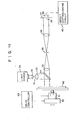
- a collimator 31 including lenses 32 and 33 is disposed on an optical path of a coherent light beam emitted from a light source 34, such as a laser device which generates a coherent light beam with a single wavelength. Collimator 31 converts the coherent light beam into parallel pencil light rays or a parallel light beam.
- a mesh plate 11, having a number of holes of identical shape arranged periodically thereon, is disposed on the optical path of the light beam for the purpose of inspection.
- a lens 35 disposed on the light path of the light beam transmitted through mesh plate 11 performs a spatial Fourier transformation of the light beam.
- Spatial filter 26 shown in Fig. 7 is located at the backward focal point of the lens 35 at which the Fourier transformed pattern of the periodic hole pattern is formed.
- the coherent light beam transmitted through mesh plate 11 includes light information on the periodic pattern and any defects, namely, it includes the periodic pattern information light component and the non-periodic pattern (defect) information light component.
- the periodic pattern information light component comprises the zeroth order diffraction light and first and higher order diffraction light.
- Light blocking area 27 of spatial filter 26 prevents transmission of the first and higher order diffraction light and circular light transmission area 28 of spatial filter 26 passes the defect information light component and the zeroth order diffraction light.
- the light passed through spatial filter 26 is inverse Fourier transformed by lens 36 located at the- focal distance f from spatial filter 26.
- a screen 37_ with a pinhole 38 and photoelectric converter 39 is located at the backward focal point of lens 36.
- the light passed through lens 36 and pinhole 38 is received by photoelectric converter 39 and converted into electrical signals which correspond to the intensity of the light.
- the electrical signals are supplied to a defect distinguishing circuit 40 which distinguishes the kind of defect in mesh plate 11 by detecting the amplitude of the electrical signals from photoelectric converter 39.
- Fig. 9 shows an example of the electrical signal waveform from photoelectric converter 39.
- the electrical signal contains a direct current component Ld because spatial filter 26 passes the zeroth order diffraction light.
- the amplitude of the electrical signal increases as shown by A l in Fig. 9.
- the part of mesh plate 11 which contains a small hole defect 10 is illuminated by the coherent light beam, the amplitude of the electrical signal is small as shown by A 2 in Fig. 9. Therefore, defect distinguishing circuit 40 can distinguish the kind of defect in mesh plate 11 by comparing the amplitude of the electrical signals with two predetermined levels L 1 and L 2 .
- Predetermined level L 1 is higher than direct current component level L d .
- Predetermined level L 2 is lower than L do
- Mesh plate 11 is supported by rotating mechanism 41 which rotates mesh plate 11 in a plane normal to the optical path of the optical system.
- Rotating mechanism 41 is further supported by a shifting mechanism 42 which shifts the mechanism at a constant rate in the plane of rotation.
- a drive controller 43 controls rotating mechanism 41 and shifting mechanism 42.
- Mesh plate 11 is laterally shifted in a direction orthogonal to the optical path of the coherent light beam, while being rotated in a plane normal to the optical path of the coherent light beam so mesh plate 11 is helically scanned by the coherent light beam.
- Spatial filter 26 always prevents the transmission of the first and higher order diffraction light even if mesh plate 11 is rotated and shifted.
- the Fourier transformed pattern shown in Fig. 4 is rotated as shown in Fig. 10.
- the first order diffraction areas 21 form a ring about the zeroth order diffraction area 20 and the higher order (more than second order) diffraction areas form rings outside the first order diffraction areas 21.
- the Fourier transformed pattern shown in Fig. 4 does not change.
- spatial filter 26 always prevents the transmission of the first and higher order diffraction light even if mesh plate 11 is rotated or shifted. Thus, it is not required to precisely align the spatial filter with the mesh plate if spatial filter 26 shown in Fig. 7 is used.
- the light passed through mesh plate 11 is Fourier transformed by lens 35.
- the periodic pattern in Fig. 8 transmits light
- the invention also is applicable to periodic patterns which reflect light.
- Fig. 11 shows an embodiment of the invention for light reflective surfaces where like reference numerals are used to designate like portions in Fig. 8.
- a beam splitter 44 is disposed between lens 35 and object 46.
- the coherent light beam passes through collimator 31 and is reflected by beam splitter 44 to impinge against alight reflecting object having a periodic pattern.
- the light reflected from object 46 is directed toward lens 35 through beam splitter 44 to enable the apparatus to detect defects in the periodic pattern.
- Fig. 12 shows another embodiment of this invention which detects the size of the defects.
- the light beam is Fourier transformed by lens 35 and split into a first and second light beam by a beam splitter 51.
- the first light beam passes through a first spatial filter 26F which has a light blocking area for preventing the transmission of the first and higher order diffraction light and a circular light transmission area for passing the zeroth order diffraction light and the defect information light component.
- the light passed through spatial filter 26F is inverse Fourier transformed by lens 36F.
- the light passed through lens 36F is directed through a pinhole 38F in screen 37F to photoelectric converter 39F.
- the second spatial filter 22S is the same as filter 22 in Fig. 6 and it is positioned at the backward focal point of lens 35.
- the second spatial filter 22S has a light blocking area 25 for blocking mainly the periodic pattern information light component and a ring-like light transmission area 23 for passing the defect information light component.
- the spatial filter 22S includes a spot-like light blocking area 24 which prevents the transmission of the zeroth order diffraction light and another light blocking area 25 which is disposed around the spot-like blocking area 24 to prevent the transmission of the first and higher order diffraction light.
- the light passed through the second spatial filter 22S is inverse Fourier transformed by a lens 36S.
- the light passed through second lens 36B then is directed through a pinhole 38S in screen 37S to photoelectric-converter 39S.
- the photoelectric converter 39S is - - connected to a size detecting circuit 52.
- the electrical signal generated by the photoelectric converter 39S corresponds to the intensity of the received light.
- the electrical signal generated by photoelectric converter 39S does not contain a direct current component as shown in Fig. 13 because second spatial filter 22S prevents the transmission of the zeroth order diffraction light.
- the amplitude of the electrical signal is porportional to the size of the defect in the periodic pattern. Therefore, size detecting circuit 52 detects the size of the defect in the periodic pattern by sensing the amplitude of the electrical signal from the photoelectric converter 39S.
- a defect pattern can be designated by coherent light, such as red laser light, and a periodic pattern can be designated by the incoherent green light at the position of screen 37F.
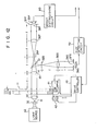
- F ig. 14 shows another embodiment of the invention. Unlike the apparatus shown in Fig. 8, the apparatus of F ig. 14 obtains information about a Fourier transformed image of a periodic pattern without using an optical system and calculates defect information from the information from the image information by arithmetic operations. More specifically, a light source 61 emits incoherent light, which is applied through a lens 62 onto a periodic pattern 63. The light which passes through the pattern 13 forms a periodic pattern image 64 of a predetermined area. Periodic pattern image 64 is sampled by an image pickup device 65 and converted into electrical analog image signals. The analog image signals are supplied to an analog digital converter 66 and are converted into digital image signals.
- the digital image signals are stored in a two-dimensional memory 67 which can store n x n digital signals. That is, the periodic pattern image 64 is split by image pickup device 65 into n x n pixells, the pixells are converted into digital signals, and the digital signals are stored at predetermined addresses.in the memory 6 7.
- the digital image signals are read out from two-dimensional memory 67 and undergo a Fourier transform operation by a Fourier transformer 68.
- the signals from Fourier transformer 68 are then stored in a two-dimensional memory 69.
- Fourier transformer 68 may be the AP-400 which is made by ANALGIC, Inc. and which achieves a high speed Fourier transformation.
- the signals are read out from two-dimensional memory 69 and then multiplied one after another by a multiplier 70. Only defect signals from these signals are stored in a memory 71.
- the multiplication at multiplier 70 is carried out according to filtering function data stored in filtering function memory 74; this takes out only the defect component signals.
- the filtering function data consists of n x n digital data.
- the area filled with digit numerals "0" correspond to-a - light blocking area as illustrated in Fig. 7, and the area filled with digit numerals "1" corresponds to a light transmission area.
- the filtering function data is a pattern formed of digital signals which correspond to n x n pixells defining the image of the spatial filter 26 of Fig. 7.
- the number of pixells which corresponds to the diameter of the light transmission area of Fig. 7 is expressed as .
- the defect signals read out from the memory 71 are supplied to an inverse Fourier transformer 72. These signals undergo an inverse Fourier transformation and are converted into pixell digital signals which represent a defect image.
- the inverse Fourier transformer 72 may be of the same type as Fourier transformer 68.
- the pixell digital signals thus - obtained are supplied to a digital-analog converter 73 and thus converted into analog defect image signals.
- the periodic patterns shown in Figs. 2 and 15 have holes arranged equidistantly, the holes of the pattern do not have to be arranged in this manner.
- the distance from a hole 75 to an adjacent hole 76 is P 1 and the distance from the hole 75 to an adjacent hole 77 is P 2 . These distances are not equal.
- Such a pattern can be used so long as the pattern is arranged periodically.
Abstract
Description
- The present invention relates to an apparatus for inspecting defects in a periodic pattern.
- In conventional apparatus for inspecting defects in a periodic pattern, the pattern is visually examined with a microscope. Since, visual examination is inherently inaccurate, another well known inspection technique employs the combination of coherent light rays and a spatial filter. In this inspection technique, -the optical information of the periodic pattern is separated into periodic pattern information and non-periodic pattern information by Fourier transformation and the non-periodic pattern information is examined by blocking the periodic pattern information with a spatial filter. This technique is disclosed in two articles in Proceedings of the IEEE, September 1969, pp. 1,634 to 1,639, "Inspection of Integrated Circuit Photomasks with Intensity Spatial Filters" by Watkins, and April 1972, pp. 447 to 448, "Intensity Spatial Filtering Applied to Defect Detection in Integrated Circuit Photomasks" by Axelrod. Also in European Patent Application Number 80 300 803.6, filed March 14, 1980, the above named inventor describes an improved apparatus using this inspection technique having an omni-directional spatial filter. A disadvantage of this technique is that the spatial filter and the examined pattern must be precisely aligned or oriented with each other.
- All the above inspecting apparatus also have the disadvantage that it is impossible to distinguish between an enlarged hole defect and a reduced hole defect. For example, a mesh plate with a number of periodic square holes may have one kind of defect which is an enlarged hole as shown in Fig. 1A and another kind of defect which is a reduced hole as shown in Fig. 1B. The inspection apparatus detects defects by solving the formula D 2 =(E-P)2 where E is light information from the examined mesh plate pattern, P is light information from an ideal periodic pattern and D is light information representing defects. When the defect is an enlarged hole, E > P and when the defect is a small hole, E < P. Accordingly, the prior art inspection apparatus cannot distinguish between the enlarged hole of Fig. lA and the reduced hole of Fig. 1B.
- Sometimes it is necessary to distinguish between an enlarged hole and a reduced hole. For example, the mesh plate with a reduced hole shown Fig. 1B can be repaired by manually removing the intruding
part 10 to thereby improve the yield. Also, there is sometimes a difference in the acceptable tolerance between an enlarged hole and a reduced hole. - It is one object of this invention to provide a new and improved apparatus for inspecting defects in a periodic pattern.
- It is another object of this invention to provide an apparatus for inspecting defects in a periodic pattern which can distinguish between an enlarged hole defect and a reduced hole defect.
- It is another object of this invention to provide an apparatus for inspecting defects in a periodic pattern which has a relatively large tolerance between- the relative positioning and orientation of a periodic pattern and the optical elements of the apparatus.
- It is a further object of this invention to provide an apparatus for inspecting defects in a periodic pattern which operates at a high speed.
- According to the invention, there is provided an apparatus for inspecting defects in a periodic pattern. The apparatus includes a device for forming a Fourier transformed pattern of the periodic pattern. A filter is then provided for passing predetermined spatial frequency ranges of the Fourier transformed pattern, the predetermined spatial frequency ranges being lower than a spatial frequency which coincides with a first order diffraction of the Fourier transformed pattern.
- Other objects and features of the invention will become apparent to those skilled in the art from the following description of a preferred embodiment of the invention, as illustrated in the accompanying drawings, in which:
- Fig. 1A shows a plan view of a mesh plate with a number of periodic square holes and an enlarged hole as an example of a periodic pattern with an enlarged hole defect;
- Fig. lB is a plan view of a mesh plate with a number of periodic square holes and a small hole as an example of a periodic pattern with a small hole defect;
- Fig. 2 shows a plan view of a mesh plate with a number of square holes as an example of a periodic pattern;
- Fig. 3 shows a schematic view of the invention;
- Fig. 4 shows a plan view of a diffraction pattern obtained by Fourier transformation of the periodic pattern shown in Fig. 2;
- Fig. 5 shows a diffraction light intensity distribution of the image shown in Fig. 4;
- Fig. 6 shows a spatial filter of the defect - inspection apparatus according to the invention of the above-mentioned European Patent Application Number 80 300 803.6;
- Fig. 7 shows an example of a spatial filter of the defect inspection apparatus according to the present invention;
- Fig. 8 is a schematic diagram of the defect inspection apparatus of the invention;
- Fig. 9 shows waveforms obtained by
photoelectric converter 39 shown in Fig. 8; - Fig. 10 shows a plan view of a diffraction image pattern formed by Fourier transformation of the periodic pattern rotated-with the mesh plate shown in Fig. 2;
- Fig. 11 shows a schematic diagram of another embodiment of the invention;
- Fig. 12 shows a schematic diagram of a further embodiment of the invention;
- Fig. 13 shows waveforms obtained by
photoelectric converter 39S shown in Fig. 12; - Fig. 14 shows a schematic diagram of another embodiment of the invention;
- Fig. 15 shows a plan view of a periodic pattern image obtained by the apparatus shown in Fig. 14;
- Fig. 16 shows filtering function data stored in a
filtering function memory 72 shown in Fig. 14; and - Fig. 17 illustrates another example of the periodic pattern.
- In the specification, the term "defect" means any factor which distorts a periodic pattern such as a different size pattern, deformation of the pattern, scratches on the pattern, dust stack to the pattern, etc. The defect inspection-apparatus according to the invention is used to detect such defects in the periodic pattern.
- A mesh plate with a mesh pattern generally is formed in a vidicon or shadow mask of a color cathode ray tube for use as an object to be inspected. Such an object, however, is not limited to a mesh plate but may be an opaque object with a periodic pattern, for example, such as used in semiconductor products.
- The basic concept of the invention will now be described referring to Figs. 2 to 7. In Fig. 2, a
mesh plate 11 is shown with a number of periodically arrangedsquare holes 12. As shown in Figs. 2 and 3, themesh plate 11 is illuminated by acoherent light beam 13. Alens 14, aspatial filter 15, and alens 16 are positioned in order on anoptical path 17 of thebeam 13, thespatial filter 15 being positioned at the focal point oflenses Lens 14 forms a spatial Fourier transformer andlens 16 forms the inverse spatial Fourier transformer. - When
coherent light beam 13 impinges uponmesh plate 11 withholes 12, the light beam from the pattern is Fourier transformed bylens 14 to form a diffraction pattern at the back focal plane oflens 14, namely at the position ofspatial filter 15, as shown in Fig. 3. In the diffraction pattern, with the orthogonal - coordinate system having and n axes, a zeroth order diffraction light component is directed to the origin to form azeroth order spot 20 and a first order diffraction light components are directed to outside of thezeroth order spot 20 to form afirst order spot 21. In this way, second and higher order diffraction light components are similarly directed to further outside of the preceding order diffraction spots. The light intensity distribution of these diffraction light components on the axis of Fig. 4 is generally illustrated by a solid line A in Fig. 5. In Fig. 4, the spot size of each diffracted light component indicates approximately the relative light intensity level. - The size of the diffraction areas and the distance between the diffraction areas is as follows. "P" denotes the pitch of the
mesh pattern 18, i.e., the interval between theadjacent holes 12, and "N" denotes the number ofholes 12 within the circle as counted in the direction of the pitch (N = 6 in Fig. 2). Then, as shown in Fig. 5, the diameter of zerothorder diffraction area 20 is
order diffraction area 20 and firstorder diffraction area 21 is
- The diffraction pattern as shown in Figs. 4 and 5 is periodic and is determined by the hole pattern in
mesh plate 11. If ahole 12 has a defect as shown Fig. lA, the defect diffracted pattern is given by a dotted line B in Fig. 5. Therefore, if a spatial filter is used to filter out the periodic diffraction pattern, e.g., aspatial filter 22 having a ring-like transmission area 23 as shown in Fig. 6, the non-periodic pattern represents the defect, namely, only the defect information may be extracted from the diffracted pattern in Fig. 4. For example, ifspatial filter 22 is placed at back focal plane oflens 14 shown in Fig. 3, a mesh pattern having only defect information light is obtained at the back focal plane oflens 16. - However, as stated above, by extracting only the defect information, it is impossible to distinguish an enlarged hole defect 9 and a reduced
hole defect 10. The primary feature of the present invention is to extract not only the non-periodic pattern information component but also the zeroth order diffraction component, which is one of the periodic pattern information components. - If light information caused by an ideal periodic pattern P comprises a direct current component of light information L and a high frequency component of light information H, light information caused by the examined mesh plate pattern E can be described as E = H+L+D which can be rewritten as L+D = E-H, where (L+D)2 = L 2+D 2+2LD.
- In the above formula, the value of 2LD is different in case of
D >0 and D<O. Therefore, it is possible to distinguish between an enlarged hole defect shown in Fig. 1A and a small hole defect shown in Fig. 1B by examining the light intensity of light information, i.e., of the direct current component, caused by an ideal periodic pattern and light information caused by defects. - The light intensity (L+D)2 is detected by a
spatial filter 26 as shown in Fig. 7.Spatial filter 26 comprises alight blocking area 27 and a circularlight transmission area 28. Circularlight transmission area 28 is a circular hole having diameter C as shown in Fig. 5, i.e.,
spatial filter 26 is placed at the back focal plane of thelens 35 shown in Fig. 3, a mesh pattern is obtained having defect information at the back focal plate of lens 16: The enlarged hole defect 9 shown in Fig. lA is detected as a bright point and thesmall hole defect 10 shown in Fig. 1B is detected as a dark spot in the mesh pattern. - In Fig. 8, an embodiment of the defect inspection apparatus according to the invention is shown. A
collimator 31 includinglenses light source 34, such as a laser device which generates a coherent light beam with a single wavelength.Collimator 31 converts the coherent light beam into parallel pencil light rays or a parallel light beam. Amesh plate 11, having a number of holes of identical shape arranged periodically thereon, is disposed on the optical path of the light beam for the purpose of inspection. Alens 35 disposed on the light path of the light beam transmitted throughmesh plate 11 performs a spatial Fourier transformation of the light beam.Spatial filter 26 shown in Fig. 7 is located at the backward focal point of thelens 35 at which the Fourier transformed pattern of the periodic hole pattern is formed. - As above-mentioned, the coherent light beam transmitted through
mesh plate 11 includes light information on the periodic pattern and any defects, namely, it includes the periodic pattern information light component and the non-periodic pattern (defect) information light component. The periodic pattern information light component comprises the zeroth order diffraction light and first and higher order diffraction light.Light blocking area 27 ofspatial filter 26 prevents transmission of the first and higher order diffraction light and circularlight transmission area 28 ofspatial filter 26 passes the defect information light component and the zeroth order diffraction light. - The light passed through
spatial filter 26 is inverse Fourier transformed bylens 36 located at the- focal distance f fromspatial filter 26. A screen 37_ with apinhole 38 andphotoelectric converter 39 is located at the backward focal point oflens 36. The light passed throughlens 36 andpinhole 38 is received byphotoelectric converter 39 and converted into electrical signals which correspond to the intensity of the light. The electrical signals are supplied to adefect distinguishing circuit 40 which distinguishes the kind of defect inmesh plate 11 by detecting the amplitude of the electrical signals fromphotoelectric converter 39. - Fig. 9 shows an example of the electrical signal waveform from
photoelectric converter 39. The electrical signal contains a direct current component Ld becausespatial filter 26 passes the zeroth order diffraction light. When the part ofmesh plate 11 which contains an enlarged hole defect 9 is illuminated by the coherent light beam, the amplitude of the electrical signal increases as shown by Al in Fig. 9. On the other hand, when the part ofmesh plate 11 which contains asmall hole defect 10 is illuminated by the coherent light beam, the amplitude of the electrical signal is small as shown by A2 in Fig. 9. Therefore, defect distinguishingcircuit 40 can distinguish the kind of defect inmesh plate 11 by comparing the amplitude of the electrical signals with two predetermined levels L1 and L2. Predetermined level L1 is higher than direct current component level Ld. Predetermined level L2 is lower than Ldo -
Mesh plate 11 is supported by rotatingmechanism 41 which rotatesmesh plate 11 in a plane normal to the optical path of the optical system. Rotatingmechanism 41 is further supported by ashifting mechanism 42 which shifts the mechanism at a constant rate in the plane of rotation. Adrive controller 43controls rotating mechanism 41 and shiftingmechanism 42.Mesh plate 11 is laterally shifted in a direction orthogonal to the optical path of the coherent light beam, while being rotated in a plane normal to the optical path of the coherent light beam somesh plate 11 is helically scanned by the coherent light beam. -
Spatial filter 26 always prevents the transmission of the first and higher order diffraction light even ifmesh plate 11 is rotated and shifted. Whenmesh plate 11 is rotated by rotatingmechanism 40, the Fourier transformed pattern shown in Fig. 4 is rotated as shown in Fig. 10. As shown in Fig. 10, the firstorder diffraction areas 21 form a ring about the zerothorder diffraction area 20 and the higher order (more than second order) diffraction areas form rings outside the firstorder diffraction areas 21. Also, whenmesh plate 11 is shifted in a direction orthogonal to the optical path of the coherent light, the Fourier transformed pattern shown in Fig. 4 does not change. Therefore,spatial filter 26 always prevents the transmission of the first and higher order diffraction light even ifmesh plate 11 is rotated or shifted. Thus, it is not required to precisely align the spatial filter with the mesh plate ifspatial filter 26 shown in Fig. 7 is used. - As mentioned with respect to Fig. 8, the light passed through
mesh plate 11 is Fourier transformed bylens 35. Although the periodic pattern in Fig. 8 transmits light, the invention also is applicable to periodic patterns which reflect light. Fig. 11 shows an embodiment of the invention for light reflective surfaces where like reference numerals are used to designate like portions in Fig. 8. Because of the light reflecting nature of the periodic pattern, abeam splitter 44 is disposed betweenlens 35 andobject 46. The coherent light beam passes throughcollimator 31 and is reflected bybeam splitter 44 to impinge against alight reflecting object having a periodic pattern. The light reflected fromobject 46 is directed towardlens 35 throughbeam splitter 44 to enable the apparatus to detect defects in the periodic pattern. - Fig. 12 shows another embodiment of this invention which detects the size of the defects. Again like reference numerals are used to designate like portions in Fig. 8. The light beam is Fourier transformed by
lens 35 and split into a first and second light beam by abeam splitter 51. The first light beam passes through a firstspatial filter 26F which has a light blocking area for preventing the transmission of the first and higher order diffraction light and a circular light transmission area for passing the zeroth order diffraction light and the defect information light component. The light passed throughspatial filter 26F is inverse Fourier transformed bylens 36F. The light passed throughlens 36F is directed through apinhole 38F inscreen 37F tophotoelectric converter 39F. - On the other hand, the second spatial filter 22S is the same as
filter 22 in Fig. 6 and it is positioned at the backward focal point oflens 35. The second spatial filter 22S has alight blocking area 25 for blocking mainly the periodic pattern information light component and a ring-likelight transmission area 23 for passing the defect information light component. The spatial filter 22S includes a spot-likelight blocking area 24 which prevents the transmission of the zeroth order diffraction light and anotherlight blocking area 25 which is disposed around the spot-like blocking area 24 to prevent the transmission of the first and higher order diffraction light. - The light passed through the second spatial filter 22S is inverse Fourier transformed by a
lens 36S. The light passed through second lens 36B then is directed through apinhole 38S inscreen 37S to photoelectric-converter 39S. Thephotoelectric converter 39S is - - connected to asize detecting circuit 52. The electrical signal generated by thephotoelectric converter 39S corresponds to the intensity of the received light. - The electrical signal generated by
photoelectric converter 39S does not contain a direct current component as shown in Fig. 13 because second spatial filter 22S prevents the transmission of the zeroth order diffraction light. The amplitude of the electrical signal is porportional to the size of the defect in the periodic pattern. Therefore,size detecting circuit 52 detects the size of the defect in the periodic pattern by sensing the amplitude of the electrical signal from thephotoelectric converter 39S. - If the size of
pinhole 38 is large, much light is received by photo-detector 39S. Therefore, rapid defect inspection is possible by usingscreen 37S with alarger pinhole 38S. Accordingly, at first,mesh plate 11 is scanned by the coherent light beam at rapid speed. When a defect is detected bysize detecting circuit 52, a speed control signal is supplied to drivecontroller 43. Then,mesh plate 11 is scanned at slow speed to determine the kind of defect by defect distinguishcircuit 40. Thus, in the embodiment shown in Fig. 12, it is possible to quickly determine the size and kind of defect. - In the embodiment shown in either Fig. 8 or Fig. 12, if a dichroic mirror is disposed between
lens 32 andlens 33, and a gelatine filter is used asspatial filter 26F, and an incoherent light beam such as green light is projected to the dichroic mirror, a defect pattern can be designated by coherent light, such as red laser light, and a periodic pattern can be designated by the incoherent green light at the position ofscreen 37F. - Fig. 14 shows another embodiment of the invention. Unlike the apparatus shown in Fig. 8, the apparatus of Fig. 14 obtains information about a Fourier transformed image of a periodic pattern without using an optical system and calculates defect information from the information from the image information by arithmetic operations. More specifically, a
light source 61 emits incoherent light, which is applied through alens 62 onto aperiodic pattern 63. The light which passes through thepattern 13 forms aperiodic pattern image 64 of a predetermined area.Periodic pattern image 64 is sampled by animage pickup device 65 and converted into electrical analog image signals. The analog image signals are supplied to an analogdigital converter 66 and are converted into digital image signals. The digital image signals are stored in a two-dimensional memory 67 which can store n x n digital signals. That is, theperiodic pattern image 64 is split byimage pickup device 65 into n x n pixells, the pixells are converted into digital signals, and the digital signals are stored at predetermined addresses.in the memory 67. - The digital image signals are read out from two-
dimensional memory 67 and undergo a Fourier transform operation by aFourier transformer 68. The signals fromFourier transformer 68 are then stored in a two-dimensional memory 69.Fourier transformer 68 may be the AP-400 which is made by ANALGIC, Inc. and which achieves a high speed Fourier transformation. The signals are read out from two-dimensional memory 69 and then multiplied one after another by amultiplier 70. Only defect signals from these signals are stored in amemory 71. The multiplication atmultiplier 70 is carried out according to filtering function data stored infiltering function memory 74; this takes out only the defect component signals. As shown in Fig. 16, the filtering function data consists of n x n digital data. The area filled with digit numerals "0" correspond to-a - light blocking area as illustrated in Fig. 7, and the area filled with digit numerals "1" corresponds to a light transmission area. In other words, the filtering function data is a pattern formed of digital signals which correspond to n x n pixells defining the image of thespatial filter 26 of Fig. 7. The number of pixells which corresponds to the diameter of the light transmission area of Fig. 7 is expressed as
- The defect signals read out from the
memory 71 are supplied to aninverse Fourier transformer 72. These signals undergo an inverse Fourier transformation and are converted into pixell digital signals which represent a defect image. Theinverse Fourier transformer 72 may be of the same type asFourier transformer 68. The pixell digital signals thus - obtained are supplied to a digital-analog converter 73 and thus converted into analog defect image signals. The apparatus of Fig. 14, though not provided with an optical system, thus can distinguish the kind of defect. - Although the periodic patterns shown in Figs. 2 and 15 have holes arranged equidistantly, the holes of the pattern do not have to be arranged in this manner. For example, as in the pattern shown in Fig. 17, the distance from a hole 75 to an adjacent hole 76 is P1 and the distance from the hole 75 to an adjacent hole 77 is P2. These distances are not equal. Such a pattern can be used so long as the pattern is arranged periodically.
Claims (11)
Applications Claiming Priority (2)
| Application Number | Priority Date | Filing Date | Title |
|---|---|---|---|
| JP143228/79 | 1979-11-07 | ||
| JP54143228A JPS60708B2 (en) | 1979-11-07 | 1979-11-07 | Defect inspection equipment |
Publications (3)
| Publication Number | Publication Date |
|---|---|
| EP0028774A2 true EP0028774A2 (en) | 1981-05-20 |
| EP0028774A3 EP0028774A3 (en) | 1982-04-07 |
| EP0028774B1 EP0028774B1 (en) | 1986-02-12 |
Family
ID=15333873
Family Applications (1)
| Application Number | Title | Priority Date | Filing Date |
|---|---|---|---|
| EP80106681A Expired EP0028774B1 (en) | 1979-11-07 | 1980-10-30 | Apparatus for detecting defects in a periodic pattern |
Country Status (4)
| Country | Link |
|---|---|
| US (1) | US4360269A (en) |
| EP (1) | EP0028774B1 (en) |
| JP (1) | JPS60708B2 (en) |
| DE (1) | DE3071422D1 (en) |
Cited By (6)
| Publication number | Priority date | Publication date | Assignee | Title |
|---|---|---|---|---|
| EP0114524A1 (en) * | 1982-12-27 | 1984-08-01 | The University Of Dayton | Production of high performance optical spatial filters |
| EP0334544A2 (en) * | 1988-03-19 | 1989-09-27 | Cabot Plastics Limited | Method and apparatus for evaluating the surface of an object |
| US5177559A (en) * | 1991-05-17 | 1993-01-05 | International Business Machines Corporation | Dark field imaging defect inspection system for repetitive pattern integrated circuits |
| FR2706048A1 (en) * | 1993-06-04 | 1994-12-09 | Marelli Autronica | Easily inspectable collimator |
| WO2007003175A2 (en) * | 2005-07-01 | 2007-01-11 | Koenig Hans Eberhard | Method and device for the analysis of ordered structures |
| CN101339360B (en) * | 2007-01-15 | 2011-08-17 | Hoya株式会社 | Pattern defect inspecting method, and pattern defect inspecting device |
Families Citing this family (27)
| Publication number | Priority date | Publication date | Assignee | Title |
|---|---|---|---|---|
| US4513441A (en) * | 1983-08-02 | 1985-04-23 | Sparta, Inc. | Image comparison system |
| US4640620A (en) * | 1983-12-29 | 1987-02-03 | Robotic Vision Systems, Inc. | Arrangement for rapid depth measurement using lens focusing |
| JPS6113318U (en) * | 1984-06-25 | 1986-01-25 | 株式会社 オ−デイオテクニカ | cassette type cleaner |
| US4873653A (en) * | 1986-04-09 | 1989-10-10 | Carl-Zeiss-Stiftung | Microscope system for providing three-dimensional resolution |
| JPH0682102B2 (en) * | 1987-02-27 | 1994-10-19 | 三菱電機株式会社 | Pattern defect inspection device and pattern defect inspection method |
| US4913524A (en) * | 1988-05-12 | 1990-04-03 | The Perkin-Elmer Corporation | Synthetic imaging technique |
| JPH01297542A (en) * | 1988-05-25 | 1989-11-30 | Csk Corp | Defect inspecting device |
| US4972258A (en) * | 1989-07-31 | 1990-11-20 | E. I. Du Pont De Nemours And Company | Scanning laser microscope system and methods of use |
| US5073006A (en) * | 1990-03-30 | 1991-12-17 | The United States Of America As Represented By The Secretary Of The Air Force | Compact 2f optical correlator |
| US5712729A (en) * | 1992-04-17 | 1998-01-27 | Olympus Optical Co., Ltd. | Artificial retina cell, artificial retina and artificial visual apparatus |
| US5644429A (en) * | 1992-07-23 | 1997-07-01 | Research Foundation Of City College Of New York | 2-dimensional imaging of translucent objects in turbid media |
| US5629768A (en) * | 1993-01-28 | 1997-05-13 | Nikon Corporation | Defect inspecting apparatus |
| US5526113A (en) * | 1994-06-21 | 1996-06-11 | Honeywell Inc. | Method and apparatus for measurement of spatial signal and noise power of imaging systems |
| US5742422A (en) * | 1995-09-19 | 1998-04-21 | Inspex, Inc. | Adjustable fourier mask |
| IL118057A0 (en) * | 1996-04-29 | 1996-09-12 | Patir Research And Dev Limited | Optical phase element |
| US5966212A (en) * | 1996-07-18 | 1999-10-12 | Pixel Systems, Inc. | High-speed, high-resolution, large area inspection using multiple optical fourier transform cells |
| WO1999027491A1 (en) * | 1997-11-20 | 1999-06-03 | Cornell Research Foundation, Inc. | A fast method and system for determining local properties of striped patterns |
| US6137570A (en) * | 1998-06-30 | 2000-10-24 | Kla-Tencor Corporation | System and method for analyzing topological features on a surface |
| US6555781B2 (en) | 1999-05-10 | 2003-04-29 | Nanyang Technological University | Ultrashort pulsed laser micromachining/submicromachining using an acoustooptic scanning device with dispersion compensation |
| US6285002B1 (en) * | 1999-05-10 | 2001-09-04 | Bryan Kok Ann Ngoi | Three dimensional micro machining with a modulated ultra-short laser pulse |
| DE10127352A1 (en) * | 2001-06-06 | 2003-01-23 | Infineon Technologies Ag | Method and device for error analysis of physical sub-objects which are arranged in a physical object in the form of a matrix, computer-readable storage medium and computer program element |
| US7262864B1 (en) * | 2001-07-02 | 2007-08-28 | Advanced Micro Devices, Inc. | Method and apparatus for determining grid dimensions using scatterometry |
| WO2004088417A1 (en) * | 2003-03-31 | 2004-10-14 | Fujitsu Limited | Photomask pattern inspecting method, photomask pattern inspecting device, and photomask pattern inspecting program |
| WO2006091913A1 (en) * | 2005-02-25 | 2006-08-31 | Nanometrics Incorporated | Apparatus and method for enhanced critical dimension scatterometry |
| US7940384B2 (en) * | 2006-12-15 | 2011-05-10 | Kla-Tencor Corp. | Systems and methods for blocking specular reflection and suppressing modulation from periodic features on a specimen |
| SG149763A1 (en) * | 2007-07-12 | 2009-02-27 | Applied Materials Israel Ltd | Method and system for evaluating an object that has a repetitive pattern |
| US10043259B2 (en) | 2016-07-25 | 2018-08-07 | PT Papertech Inc. | Facilitating anomaly detection for a product having a pattern |
Citations (3)
| Publication number | Priority date | Publication date | Assignee | Title |
|---|---|---|---|---|
| US3614232A (en) * | 1968-11-25 | 1971-10-19 | Ibm | Pattern defect sensing using error free blocking spacial filter |
| US3790280A (en) * | 1972-05-03 | 1974-02-05 | Western Electric Co | Spatial filtering system utilizing compensating elements |
| EP0017371A1 (en) * | 1979-03-19 | 1980-10-15 | Kabushiki Kaisha Toshiba | Apparatus for inspecting defects in a periodic pattern |
-
1979
- 1979-11-07 JP JP54143228A patent/JPS60708B2/en not_active Expired
-
1980
- 1980-10-30 EP EP80106681A patent/EP0028774B1/en not_active Expired
- 1980-10-30 US US06/202,320 patent/US4360269A/en not_active Expired - Lifetime
- 1980-10-30 DE DE8080106681T patent/DE3071422D1/en not_active Expired
Patent Citations (3)
| Publication number | Priority date | Publication date | Assignee | Title |
|---|---|---|---|---|
| US3614232A (en) * | 1968-11-25 | 1971-10-19 | Ibm | Pattern defect sensing using error free blocking spacial filter |
| US3790280A (en) * | 1972-05-03 | 1974-02-05 | Western Electric Co | Spatial filtering system utilizing compensating elements |
| EP0017371A1 (en) * | 1979-03-19 | 1980-10-15 | Kabushiki Kaisha Toshiba | Apparatus for inspecting defects in a periodic pattern |
Non-Patent Citations (3)
| Title |
|---|
| APPLIED OPTICS, Vol. 19, No. 7 April 1980, New York A. IWAMOTO et al. "Rotation-, Shift-, and Magnification-insensitive Periodic-pattern-defects Optical Detection System" pages 1196 to 1200 * |
| IBM JOURNAL OF RESEARCH AND DEVELOPMENT Vol. 17, No. 6, November 1973 A.L. FLAMHOLZ et al. "Dimensional Measurement and Defect Detection Using Spatial Filtering" pages 509 to 518 * |
| PROCEEDINGS OF THE IEEE, Vol. 57, No. 9, September 1969 L.S. WATKINS "Inspection of Integrated Circuit Photomasks with Intensity Spatial Filters" pages 1634 to 1639 * |
Cited By (8)
| Publication number | Priority date | Publication date | Assignee | Title |
|---|---|---|---|---|
| EP0114524A1 (en) * | 1982-12-27 | 1984-08-01 | The University Of Dayton | Production of high performance optical spatial filters |
| EP0334544A2 (en) * | 1988-03-19 | 1989-09-27 | Cabot Plastics Limited | Method and apparatus for evaluating the surface of an object |
| EP0334544A3 (en) * | 1988-03-19 | 1990-09-26 | Cabot Plastics Limited | Method and apparatus for evaluating the surface of an object |
| US5177559A (en) * | 1991-05-17 | 1993-01-05 | International Business Machines Corporation | Dark field imaging defect inspection system for repetitive pattern integrated circuits |
| FR2706048A1 (en) * | 1993-06-04 | 1994-12-09 | Marelli Autronica | Easily inspectable collimator |
| WO2007003175A2 (en) * | 2005-07-01 | 2007-01-11 | Koenig Hans Eberhard | Method and device for the analysis of ordered structures |
| WO2007003175A3 (en) * | 2005-07-01 | 2007-05-03 | Hans Eberhard Koenig | Method and device for the analysis of ordered structures |
| CN101339360B (en) * | 2007-01-15 | 2011-08-17 | Hoya株式会社 | Pattern defect inspecting method, and pattern defect inspecting device |
Also Published As
| Publication number | Publication date |
|---|---|
| DE3071422D1 (en) | 1986-03-27 |
| US4360269A (en) | 1982-11-23 |
| JPS5667486A (en) | 1981-06-06 |
| EP0028774A3 (en) | 1982-04-07 |
| EP0028774B1 (en) | 1986-02-12 |
| JPS60708B2 (en) | 1985-01-09 |
Similar Documents
| Publication | Publication Date | Title |
|---|---|---|
| EP0028774A2 (en) | Apparatus for detecting defects in a periodic pattern | |
| EP0017371B1 (en) | Apparatus for inspecting defects in a periodic pattern | |
| US5471066A (en) | Defect inspection apparatus of rotary type | |
| US6366690B1 (en) | Pixel based machine for patterned wafers | |
| US3614232A (en) | Pattern defect sensing using error free blocking spacial filter | |
| EP0500293B1 (en) | Particle detection method and apparatus | |
| US5805278A (en) | Particle detection method and apparatus | |
| KR100246268B1 (en) | Apparatus for optical inspection of patterned substrates | |
| US6104481A (en) | Surface inspection apparatus | |
| US4898471A (en) | Particle detection on patterned wafers and the like | |
| US5659390A (en) | Method and apparatus for detecting particles on a surface of a semiconductor wafer having repetitive patterns | |
| GB2051349A (en) | Automatic defecting inspection apparatus | |
| CH617772A5 (en) | ||
| JPS6182147A (en) | Method and device for inspecting surface | |
| US3586865A (en) | Method of,and apparatus for,inspecting the shape of small objects | |
| JPS6036013B2 (en) | Metal surface defect inspection method | |
| KR970000781B1 (en) | Foreign matter detection device | |
| RU2152589C1 (en) | Process controlling position of fiber, method of control over position of fiber and device to measure distance to surface | |
| EP0035720A1 (en) | Apparatus for inspecting an object by light | |
| JPH0783840A (en) | Rotary defect inspection device | |
| JP2000509825A (en) | Optical scanning device | |
| JPH0682373A (en) | Inspection of defect | |
| JP3218726B2 (en) | Foreign matter inspection device | |
| JPS62119439A (en) | Measurement of etched pit on monocrystalline surface | |
| JP3556324B2 (en) | Hologram inspection apparatus and method |
Legal Events
| Date | Code | Title | Description |
|---|---|---|---|
| PUAI | Public reference made under article 153(3) epc to a published international application that has entered the european phase |
Free format text: ORIGINAL CODE: 0009012 |
|
| AK | Designated contracting states |
Designated state(s): DE FR GB IT NL |
|
| PUAL | Search report despatched |
Free format text: ORIGINAL CODE: 0009013 |
|
| AK | Designated contracting states |
Designated state(s): DE FR GB IT NL |
|
| 17P | Request for examination filed |
Effective date: 19801030 |
|
| RAP1 | Party data changed (applicant data changed or rights of an application transferred) |
Owner name: KABUSHIKI KAISHA TOSHIBA |
|
| GRAA | (expected) grant |
Free format text: ORIGINAL CODE: 0009210 |
|
| AK | Designated contracting states |
Designated state(s): DE FR GB |
|
| ET | Fr: translation filed | ||
| REF | Corresponds to: |
Ref document number: 3071422 Country of ref document: DE Date of ref document: 19860327 |
|
| PLBE | No opposition filed within time limit |
Free format text: ORIGINAL CODE: 0009261 |
|
| STAA | Information on the status of an ep patent application or granted ep patent |
Free format text: STATUS: NO OPPOSITION FILED WITHIN TIME LIMIT |
|
| 26N | No opposition filed | ||
| PGFP | Annual fee paid to national office [announced via postgrant information from national office to epo] |
Ref country code: FR Payment date: 19941011 Year of fee payment: 15 |
|
| PGFP | Annual fee paid to national office [announced via postgrant information from national office to epo] |
Ref country code: GB Payment date: 19941020 Year of fee payment: 15 |
|
| PGFP | Annual fee paid to national office [announced via postgrant information from national office to epo] |
Ref country code: DE Payment date: 19941021 Year of fee payment: 15 |
|
| PG25 | Lapsed in a contracting state [announced via postgrant information from national office to epo] |
Ref country code: GB Effective date: 19951030 |
|
| GBPC | Gb: european patent ceased through non-payment of renewal fee |
Effective date: 19951030 |
|
| PG25 | Lapsed in a contracting state [announced via postgrant information from national office to epo] |
Ref country code: FR Effective date: 19960628 |
|
| PG25 | Lapsed in a contracting state [announced via postgrant information from national office to epo] |
Ref country code: DE Effective date: 19960702 |
|
| REG | Reference to a national code |
Ref country code: FR Ref legal event code: ST |