EP0029121B1 - Shared storage arrangement for multiple processor systems with a request select ring - Google Patents
Shared storage arrangement for multiple processor systems with a request select ring Download PDFInfo
- Publication number
- EP0029121B1 EP0029121B1 EP80106264A EP80106264A EP0029121B1 EP 0029121 B1 EP0029121 B1 EP 0029121B1 EP 80106264 A EP80106264 A EP 80106264A EP 80106264 A EP80106264 A EP 80106264A EP 0029121 B1 EP0029121 B1 EP 0029121B1
- Authority
- EP
- European Patent Office
- Prior art keywords
- processor
- request
- ring
- latch
- storage
- Prior art date
- Legal status (The legal status is an assumption and is not a legal conclusion. Google has not performed a legal analysis and makes no representation as to the accuracy of the status listed.)
- Expired
Links
Images


Classifications
-
- G—PHYSICS
- G06—COMPUTING; CALCULATING OR COUNTING
- G06F—ELECTRIC DIGITAL DATA PROCESSING
- G06F13/00—Interconnection of, or transfer of information or other signals between, memories, input/output devices or central processing units
- G06F13/14—Handling requests for interconnection or transfer
- G06F13/16—Handling requests for interconnection or transfer for access to memory bus
- G06F13/18—Handling requests for interconnection or transfer for access to memory bus based on priority control
Definitions
- This invention relates to a shared storage arrangement for multiple processor systems including a plurality of processors connected to a shared storage unit.
- Patent US-A-3,706,974 (R. L. Patrick et al) assigned to International Business Machines Corporation, filed October 27, 1971, published December 19, 1972, describes a system comprising a plurality of devices interconnected in a loop arrangement by an enabling or "Go" line.
- a controlling unit is coupled in parallel to all the devices. Each device actuates its leg of the "Go” line if it was the device granted last service or if it does not have a service request present.
- the connection of a requesting device to the controlling unit results only if it receives a "Go" signal on the "Go" line from the device preceding it on the loop.
- This system requires a "Go" signal to propagate clear around the loop before service can be granted. This reduces the systems performances.
- Patent US-A-3,832,692 (Henzel et al) describes a priority network including a multiple line bus coupled with a plurality of priority seeking devices, the priority of each device being dependent upon its proximity to the input end of the bus. Each device determines whether it has priority or not by looking back at the priority indications of two or more previous devices.
- the shared storage arrangement is used in a data processing system comprising a plurality of processors, each of them having facilities for processing data in accordance with programmed instruction sequences and for generating storage request signals, at least one common shared storage unit, for storing data processing information in a plurality of addressable locations, a storage control unit interconnected with the shared storage unit for controlling access to the addressable locations in the shared storage unit to fetch or store data processing information in the addressable locations upon storage requests generated by the processors and individual processor interconnect means respectively associated with each processor and activatable to interconnect them with the storage control unit.
- the storage control unit is responsive to signals on request lines from the processors to selectively activate the processor interconnect means and thereby interconnect a selected processor to the shared storage unit for transfer of control, address, and data signals therebetween.
- the storage control unit comprises a request select ring connected to the processors according to a logical ring configuration.
- a request select ring connected to the processors according to a logical ring configuration.
- the select ring comprises a processor request latch associated with each processor, settable in response to a request signal from its associated processor, a processor accept latch associated with each processor for providing an accept signal to its associated processor when a request therefrom has been accepted by the select ring, a last service latch associated with each processor, settable in response- to the accept signal provided by the processor accept latch, a lookahead ring circuit associated with each processor for providing a Go signal in response to signals from the last service latches, the accept latches and the request latches, of at least a group of processors and in response to a Go signal from a similar lookahead ring circuits responsive to signals from a preceding group of processors on the ring, a master request latch responsive to a request signal from any set request latch AND a Go signal from the lookahead ring circuit associated with the processor preceding the requesting processor on the ring, for setting the processor accept latch of each processor, whereafter the last service latch is set to hold the current accept signal in order that the determination of the next requesting processor
- the invention also provides a Test and Set operation, whereby processor A, as an example, would seize the shared storage for two memory cycles, accomplishing both test and set before processor B has access to the shared storage.
- the Test and Set operation allows the selected CPU to freeze the ring.
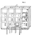
- FIG 1 illustrates one arrangement of eight central processing units (CPU's 1-8 positioned to form a letter "H" as viewed from above.
- the CPU's may be of the type described in US-A-4,047,161 (M. I. Davis entitled: “Task Management Apparatus") or in the "Series/1 Digest", GS 360-0061, copyright 1977, 1978, IBM Corporation.
- each 1,8 meter rack is positioned in the front and four others 5-8 of equal size, in 1,8 meter racks, are in the rear.
- a frame positioned in between each set of four processors houses the shared storage card file 10.
- each 1,8 meter rack is bolted to the one next to its so that all eight racks, along with the shared storage unit, create one solid grounded frame system.
- the "H" configuration is just one of many different configurations that can be used. It is preferably done in this fashion to make use of flat cable internally located in the frames.
- Each of the processors such as processor 4, has a number of associated units such as the printer 11 and display station 12.
- the processor may have an input/output expansion unit 14, a sensor I/O unit 15, a diskette unit 16 and a disk storage unit 17.
- the storage for each CPU is up to 256 KB in size (from 64 kB to 256 kB).
- the Shared Storage card file 10 has up to 512 KB of storage (from 64 KB to 512 KB) on individual circuit cards. Shared storage addresses are fixed to start at location (hexadecimal) 200.000 to insure its address is greater than any attached future CPU.
- the hexadecimal notation is a convenient means of denoting a binary number, groups of 4 bits being expressed by their equivalent in the hexadecimal number system. Thus in hexadecimal number "200.000", hexadecimal "2" represents binary number "0010" and hexadecimal "0" represents binary number '0000".
- the storage in the Shared Storage card file is accessible to all attached CPU's.
- the attached CPU's have no means of direct communication with each other, but communicate only through the shared storage unit 10.
- Program Interrput/Digital Output (PI/DO) or other communications features may be connected between CPU's for interrupt capability.
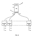
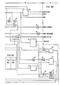
- the multiple processor system of figure 1 is illustrated in a more diagramatic form. It includes the CPU's 1-8, the Shared Storage card file 10, and a number of interconnecting cables 20 enabling transmission of control, address and data information between the CPU's 1-8 and Shared Storage card file 10 by way of interface cards 21.
- Each CPU is attached to the Shared Storage card file via two flat cables from top card connectors on the CPU Address Expansion card cables to top card connectors on its CPU Interface card.
- a set of wires is dedicated to each CPU so that the request and storage address for the next CPU to be serviced can be sitting on the cables into the Shared Storage card file ready to be serviced immediately upon completion of the last CPU service without delay.
- the length of these cables is typically between 2 and 7 meters.
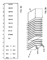
- the Shared Storage card file is typically packaged in a card file ( Figures 3A and 3B), containing a number of card sockets such as card sockets A-Q and a power supply 23.
- This card file contains up to four CPU interface cards (A-D), a Storage Control Unit (SCU) card (F) and an associated extender card (G) to provide a path for signals from the top of the SCU card to the card file board, and up to eight 64 K byte storage cards (H-Q).
- Each of the interface cards (A-D) handles attachment of two of the processors.
- the CPU/CPU Interface card interface for each attached CPU consists of forty lines as shown in Figure 4 and as also represented on the left side of Figure 6A.
- the Shared Storage Bus is a bidirectional dual purpose 26-bit bus (bits 0-22, PO, P 1 and P2). The bus is used for both the transfer of the storage address and the transfer of data between the attached CPU's and the Shared Storage.
- Bits 0-22, PO, P and P2 are used to transfer the Shared Storage Address from the CPU to the Shared Storage card file.
- the Storage Address bits are valid from the rise of the Request line to the rise of the Gate CSX&Y line (see Figure 7).
- the Storage Address bits and their usage are shown below.
- Bits 0-15, PO and P1 are used for Data Transfer between the CPU and Shared Storage.
- Test and Reset Other instructions which may be used but which require inversion of the logic, i.e., really Test and Reset are Move Byte and Zero, Move Word and Zero, Test Bit and Invert, and Test Bit and Reset.
- This interface consists of 40 lines, not illustrated. However, these lines are essentially the same as those described in connection with Figure 4 with the following exceptions:
- This interface consists of 80 lines. These lines are shown in Figure 5 and are also represented on the right side of Figure 6B.
- a typical CPU Interface card 21, Figures 2 and 6A has connectors for the two cables which carry the signals for communication with the Address Expansion card of the attached CPU.
- One CPU Interface card has four connectors so it can accommodate up to two CPU's.
- the CPU Interface card contains logic for the 26-bit Shared Storage bus, gating logic for signal lines from the CPU Interface card to the Storage Control Unit (SCU) card, and drivers and receivers for the CPU/CPU Interface card interface.
- SCU Storage Control Unit
- SCU Storage Control Unit
- the storage Control Unit (SCU) card 18 18, Figures 2, 6A and 6B, has connectors for the three flat cables to the Extender Card.
- the SCU card, Figures 6A contains:
- Test and set allows the selected CPU to freeze the ring so that it does not advance to another CPU.
- the Storage Address is checked to determine if it is within the domain of installed storage. If it is not, an Invalid Storage Address (ISA) signal is generated.
- ISA Invalid Storage Address
- Test and Set is held up from one CPU for greater than a predetermined amount of time then a Storage Parity Check is set in that CPU and requests from that CPU are blocked until Test and Set drops.
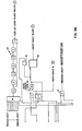
- a Request signal from the CPU handled by this portion of the interface card 21 feeds receiver 51, Figure 6A, which in turn is directed to the Select Ring logic 52.
- Select Ring logic 52 determines which CPU has access to Shared Storage and sends an accept signal through Driver block 53 to the appropriate interface card and back to the requesting processor.
- the Accept signal also sets the Accept Flip Latch Holdover 55.
- the Accept Latch Holdover output goes to AND circuit 56 which gates Bus 50 through a set of AND circuits generally represented by 57 to the Storage Control Unit Card 18 and to the Storage Address Register 60.
- the signal on line 58 which is the logical OR of the eight Accept signals within Select Ring logic 52 is gated at AND circuit 59 receiving on its other input a Gate Card Select Not signal (by way of AND circuit 62 and AND Invert circuit 64).
- the output pulse from AND circuit 59 which is approximately 55 nanoseconds, sets the data on bus 50 into Storage Address Register 60.
- Gate Card Select does become active, it is gated at AND circuit 77 by the output of Invalid Storage Address logic 76 (figure 6B).
- ISA latch 78 will be set if ISA logic 76 determines that an Invalid Storage Address has been selected. The output of the ISA latch 78 is sent to the requesting processor through driver 79, Figure 6A.
- Signal Gate CSX&Y from AND circuit 63, Figure 6A is sent in true and inverted form (by means of inverter 94) into AND circuits 93 and 92 respectively ( Figure 6B).
- the Parity Check block 70, Figure 6B checks the Storage Address Register contents (transmitted by AND circuit 92) for odd byte parity.
- the Parity Check block 70 gates AND circuit 71, Figure 6B, and sets the SAR parity latch 72 if the address register's parity was incorrect.
- the output from the SAR parity latch is sent to the requesting processor through driver 73, Figure 6A.
- Card Select and CSX&Y logic within Card Select block 66, Figure 6B generate sixteen (16) unique card select lines, four (4) common CSX lines and four (4) common CSY lines. These signals are generated from the decoding of the Storage Address Register bits and are timed by Gate Card Select and Gate CSX&Y.
- Invert block 97, AND circuit 98 and Invert block 99, Figure 6A are used to control the direction which Bus 50 is carrying data.
- AND circuit 98 and Driver 83 are degated when Gate CSX&Y is inactive. This allows Bus 50, which is carrying the Shared Storage Address to be gated through AND circuit 57 and hence to the Storage Address Register 60.
- Gate CSX&Y becomes active and the shared Storage Operation is a Write operation to storage, that is, Write SCU Strobe is active from AND circuit 69, and circuit 98 and Driver 83 are still blocked, Bus 50 continues to be gated through AND circuit 57. Data will pass through the SCU card 18 by way of driver 67, Figure 6B.
- Gate CSX&Y became active and the shared storage operation was a Read from storage, that is, Write SCU strobe is not generated, then the output from inverter 97 would be at a logical 1 and thus gate AND circuit 98 would be enabled. This in turn degates AND circuit 57 and enables driver 83. After the appropriate storage access time, data from storage enters the SCU via receiver 81, Figure 6B, and leaves the SCU via driver 82, Figure 6A. This allows interface card 21 to redrive the storage data through driver 83 to Bus 50.
- AND circuits 84 and 85 serve a Write strobing function.
- Gate CSX&Y also removes the Request line to block 51, Figure 6A, which then removes it from the Select Ring logic 52. This causes Select Ring logic 52 to drop line 58.
- AND circuit 95 allows data to come from storage through Driver 82 after Gate CSX&Y becomes active. The fact that it is a Read operation rather than a Write operation is indicated by Inverter 96. If the Shared Storage Request is a Write operation, the Write Op 0/1 lines will become active at the beginning of the request as shown in the timing chart, Figure 7, and remain active until the Shared Storage Write cycle is completed.
- Test and Set Pulse Another item of interest in the timing chart, Figure 7, is the Test and Set Pulse. This signal was described earlier and is used to block the Select Ring logic 52 from advancing to the next processor between the Fetch and the Store of the Test and Set operation.
- the Test and Set signal becomes active soon after the rise of the Gate Card Select associated with the fetch portion of the operation by way of Receiver circuit 90 and remains active until the fall of Gate Card Select associated with the store portion of the operation.
- Some multiple processor systems operation with delays because the select ring advances at the rate of an internal clock. If a request from a CPU just missed being selected, it would have to wait while the Select Ring proceeded clear around the ring before it could be serviced.
- next CPU to be serviced gets the next cycle. If there is a cycle in progress, the next CPU to be serviced is partially set up during the current service time, so that the next cycle can start shortly after completion of the current cycle.
- the Select Ring 52 herein uses CPU lookahead. This contrasts with US-A-3,706,974 which required the GO line to propage clear around the ring before service could be granted.
- the CPU lookahead bypass stages in the ring and speeds up response time.
- Test and Set feature allows the selected CPU to freeze the ring so it does not advance to another CPU.
- Figure 7 shows the Select Ring interface timings and Figures 8A-8D show the Select Ring logic with certain ring logic common to all processors.
- Select Ring logic 52 is shown in considerable detail in Figures 8A-8D which include necessary to implement one processor selection for the Select Ring as well as certain common logic that is provided for handling up to eight processors.
- the start of the Select Ring operation is with inputs to the Processor 0 Request Input Gates 110, Figure 8A.
- the input signal lines to block 110 are Request In from processor 0, (also referred to as Request Block 51 in Figure 6A), Last Service Polarity Hold 0 (PH) and Test and Set.
- Another condition is Test and Set Not and Request In from processor 0 stored by Processor 0 Request Latch 101 by way of Input Gates 110. This logic insures that the proper CPU Shared Storage Request is processed if Test and Set is active.
- the output from AND circuit 114 among other places is directed to the Master Request Set Gate 113.
- the Master Request Set Gate is an OR circuit.
- Each processor in the Select Ring has an AND circuit 114 in the Select Ring Logic.
- the output of Block 113 in turn goes to the Master Request latch 102, Figure 8B.
- the Master Request Latch 102 will set if Accept Holdover latch driver 54 in Figure 6A and the output of block 113. Figure 8A, are active.
- the output of Master Request Latch 102 is directed to a continuously triggered Single Shot Block 119 which is deconditioned 100 nanoseconds after the Master Request latch 102 is set.
- the output of the Single Shot 119 is referred to as Master Request Delay and is one input into the Processor 0 Accept latch 103 ( Figure 8C).
- the 100 ns delay is necessary to allow the Common Lookahead ring circuitry block 105 to settle out. This is the period of time during which the Lookahead Ring 105 decides which processor will have its request accepted.
- the Lookahead Ring circuitry 105 ( Figure 8D) is duplicated for every processor and provides for four processor lookahead.
- the longest logic path required to process a request by the Logic Lookahead Ring involves four stages of delay.
- a Lookahead Ring accommodating four processors is chosen as the optimum ring due to technology considerations. Obviously, a Lookahead Ring accommodating 8 processors provides the fastest ring settle out time.
- Processor 0 is at the head of the ring, then Processor 7 would be the last processor in a counterclockwise direction. If Processor 2 was the last one to be serviced, the ring would prioritize requests from Processor 3, then Processor 4, Processor 5, etc., in that order. In actuality because of the lookahead operation, all eight processors scanned from the last processor serviced can be scanned and serviced in the same amount of time as it would take to scan only two processors in a ring without look ahead.
- Lookahead ring 105 includes a five-way AND/OR circuit arrangement which receives various inputs from the Ring circuits in Figure 8.
- the Lookahead Ring logic for four processors is implemented according to the following Boolean equation for each processor on the ring.
- Processor Accept latch block 103 on the Set side is the Accept Latch Holdover Not which is derived from block 54, Figure 6A.
- block 103 will set and its output is then directed to several places. First of all, it is supplied to the NAND Block 117 which returns to Driver 53 in Figure 6A. This provides an "Accept 0" signal.
- Another use of the output from Processor 0 Accept latch 103 is to the Last Service clocking circuitry 107, Figure 8B. The purpose of this circuitry is to produce a glitch pulse of predicatable width. A signal at the input of circuit 107 proceeds through a number of inverter stages which determine the width of the pulse.
- the original signal is ANDed together with the derived pulse from the Inverter circuits to make up the particular pulse required from the output of Circuit 107.
- Another circuit which receives the output from Processor 0 Accept latch 103 is the Last Service 0 latch block 104.
- Each Select Ring processor has a "Last Service” latch which gets set when its corresponding Processor's Request has been accepted by the Ring logic.
- Last Service Generator 109 unique to Last Service 0 latch 104. This circuit provides for two things. It selects Last Service 0 latch at cold start time and if Last Service latch is not set on any processor connected to the Select Ring this circuitry sets Last Service 0 latch. The Last Service signals are essential for correct select Ring operation.
- Block 112 comprises a Master Request Gate for which AND circuit 111 provides an input from Processor 0. Block 112 merely resets the Master Request latch 102 at the appropriate time.
- Single Shot Block 121 provides a 2 microsecond Time Out after the Master Request Latch 102 is set.
- the output of block 121 feeds the reset side of the Master Request Latch.
- the operation of the single shot keeps the ring from dead-locking due to component failure or noise filtering into the Select Ring Logic.
- the sequence is as follows.
- the signals are shown for Processor 0 but apply to any of the other processors 1-7 which may be referred to as processor N.
- the Processor Request 0 involving block 1.01 is received by the Ring Logic, previously described. That, and the fact that the Master Request latch 102 is not active, is enough to set the request. With some logic delay time, the Master Request latch 102 is then set.
- the Single Shot 119 provides for 100 nanoseconds delay which is referred to as Master Request Latch Delayed. Within a certain amount of logic delay, according to the technology, the Accept 0 latch 103, Figure 8C, is set. Also see driver 53, Figure 6A.
- an Accept Latch Holdover signal from block 54, Figure 6A comes into the Select Ring logic, Figures 8A-8D, and degates Master Request latch 102, Figure 8B, and Processor 0 Accept latch 103, Figure 8C.
- the requesting processor will drop its request and in turn the Select Ring logic Processor 0 Request Latch 101 will also reset.
- the Master Request latch 102 is also reset. This, in turn, resets Processor 0 Accept latch 103.
- the Select Ring logic has essentially done its function and is waiting for the Accept Latch Holdover 54 to drop. Once that drops, another processor or shared storage request can be filled, and the process and the timing starts all over.
- the Last Service 0 latch 104 is set as a function of Processor 6 Accept latch 103 and will remain set until another processor shared storage request has been filled. Last service 0 latch 104 is set >55 ns after processor 0 accept latch becomes valid.
- Test and Set signal which comes from driver 90 in Figure 6A, gates the input to Processor 0 Request Input block 110, Figure 8A.
- This line when it is active allows only that processor which has its Last Service latch set to fill a new request from the processor. This will continue until this particular line drops out. It becomes active at Gate Card Select Time and Falls when Gate Card Select goes away.
Description
- This invention relates to a shared storage arrangement for multiple processor systems including a plurality of processors connected to a shared storage unit.
- Systems of this nature have been described wherein multiple central processing units communicate through a shared storage. Many times a single bus structure is shared by all of the units on a time-shared basis which may lead to delays time. In many cases, access to the shared or common memory is set up on a prioritized basis, and it is known to provide interface units in a multiple processing system to resolve priority among the various processors requesting service.
- Thus, the article "Dynamic Resolution of Memory Access Conflicts" by J. M. Daniel, published in IEEE Transactions on computers, volume C-20, No. 12, 1971 pp. 1583-1586, describes a method for designing and implementing a dynamic priority assignment memory-access conflict-resolution circuit for use in multiprocessing systems with K processors. A state table is first made according to a decision rule establishing a cyclic priority. Then, the state table is transformed into logic equations using map simplification or other means. The logic circuit obtained from the logic equations produces an output on only one line for each arbitration among processors. Of source, such a circuit can be used only for a system with K processors and if a supplementary processor is added in the system, a new circuit must be designed.
- Patent US-A-3,706,974 (R. L. Patrick et al) assigned to International Business Machines Corporation, filed October 27, 1971, published December 19, 1972, describes a system comprising a plurality of devices interconnected in a loop arrangement by an enabling or "Go" line. A controlling unit is coupled in parallel to all the devices. Each device actuates its leg of the "Go" line if it was the device granted last service or if it does not have a service request present. The connection of a requesting device to the controlling unit results only if it receives a "Go" signal on the "Go" line from the device preceding it on the loop. This system requires a "Go" signal to propagate clear around the loop before service can be granted. This reduces the systems performances.
- Patent US-A-3,832,692 (Henzel et al) describes a priority network including a multiple line bus coupled with a plurality of priority seeking devices, the priority of each device being dependent upon its proximity to the input end of the bus. Each device determines whether it has priority or not by looking back at the priority indications of two or more previous devices.
- But none of the above documents describes an arrangement such as the object of the invention in which a lookahead feature speeds up responses to request signals from the processors in a ring configuration by partially setting up, during the current service time, the processor to be serviced next so that the new cycle can start quickly after completion of the current cycle.
- The shared storage arrangement according to the present invention is used in a data processing system comprising a plurality of processors, each of them having facilities for processing data in accordance with programmed instruction sequences and for generating storage request signals, at least one common shared storage unit, for storing data processing information in a plurality of addressable locations, a storage control unit interconnected with the shared storage unit for controlling access to the addressable locations in the shared storage unit to fetch or store data processing information in the addressable locations upon storage requests generated by the processors and individual processor interconnect means respectively associated with each processor and activatable to interconnect them with the storage control unit. The storage control unit is responsive to signals on request lines from the processors to selectively activate the processor interconnect means and thereby interconnect a selected processor to the shared storage unit for transfer of control, address, and data signals therebetween.
- The storage control unit comprises a request select ring connected to the processors according to a logical ring configuration. When two CPU requests come in simultaneously, the next one around the ring from the last processor serviced gets the next cycle. If there is a cycle in progress, the next processor to be serviced is partially set up during the current service time so that the new cycle can start quickly after completion of the current cycle.
- The select ring comprises a processor request latch associated with each processor, settable in response to a request signal from its associated processor, a processor accept latch associated with each processor for providing an accept signal to its associated processor when a request therefrom has been accepted by the select ring, a last service latch associated with each processor, settable in response- to the accept signal provided by the processor accept latch, a lookahead ring circuit associated with each processor for providing a Go signal in response to signals from the last service latches, the accept latches and the request latches, of at least a group of processors and in response to a Go signal from a similar lookahead ring circuits responsive to signals from a preceding group of processors on the ring, a master request latch responsive to a request signal from any set request latch AND a Go signal from the lookahead ring circuit associated with the processor preceding the requesting processor on the ring, for setting the processor accept latch of each processor, whereafter the last service latch is set to hold the current accept signal in order that the determination of the next requesting processor to be serviced, which is the first requesting processor around the ring from the last processor serviced, can be set up in the lookahead ring circuit as soon as the processor accept latch is reset so that a new cycle can start quickly after completion of the current cycle.
- The invention also provides a Test and Set operation, whereby processor A, as an example, would seize the shared storage for two memory cycles, accomplishing both test and set before processor B has access to the shared storage. The Test and Set operation allows the selected CPU to freeze the ring.
- For a better understanding of the present invention, together with other and further advantages and features thereof, reference is made to the description taken in connection with the accompanying drawings, which is the description of at least one way of carrying the invention.
- Referring to the drawings:
- Figure 1 is a perspective view of a multiple processing system incorporating the shared storage feature in accordance with the present invention.
- Figure 2 is a block diagram of a multiple processing system comparable to that illustrated in Figure 1.
- Figure 3A is a diagram of the layout of a shared storage card file useful in the systems of Figures 1 and 2, while Figure 3B is a pictorial representation of such card file.
- Figure 4 illustrates the interface lines between the central processing units and the shared storage.
- Figure 5 illustrates the interface lines between the storage control unit and the storage card.
- Figures 6A and 6B, when arranged as shown in Figure 6C, illustrate various interface and storage control unit logic utilized in the systems of Figures 1 and 2.
- Figure 7 is a timing diagram for the central processing unit/shared storage interface.
- Figures 8A-8D, when arranged as shown in Figure 8E illustrate a select ring and associated logic useful in handling requests for the storage shared by the central processing units.
- The following abbreviations are sometimes used herein:

- Figure 1 illustrates one arrangement of eight central processing units (CPU's 1-8 positioned to form a letter "H" as viewed from above. The CPU's (processors) may be of the type described in US-A-4,047,161 (M. I. Davis entitled: "Task Management Apparatus") or in the "Series/1 Digest", GS 360-0061, copyright 1977, 1978, IBM Corporation.
- Four of the processors 1-4 each mounted in an 1,8 meter rack, are positioned in the front and four others 5-8 of equal size, in 1,8 meter racks, are in the rear. A frame positioned in between each set of four processors houses the shared
storage card file 10. Typically, each 1,8 meter rack is bolted to the one next to its so that all eight racks, along with the shared storage unit, create one solid grounded frame system. The "H" configuration is just one of many different configurations that can be used. It is preferably done in this fashion to make use of flat cable internally located in the frames. - Each of the processors, such as
processor 4, has a number of associated units such as the printer 11 and display station 12. In addition, the processor may have an input/output expansion unit 14, a sensor I/O unit 15, adiskette unit 16 and adisk storage unit 17. - The storage for each CPU is up to 256 KB in size (from 64 kB to 256 kB). The Shared
Storage card file 10 has up to 512 KB of storage (from 64 KB to 512 KB) on individual circuit cards. Shared storage addresses are fixed to start at location (hexadecimal) 200.000 to insure its address is greater than any attached future CPU. The hexadecimal notation is a convenient means of denoting a binary number, groups of 4 bits being expressed by their equivalent in the hexadecimal number system. Thus in hexadecimal number "200.000", hexadecimal "2" represents binary number "0010" and hexadecimal "0" represents binary number '0000". The storage in the Shared Storage card file is accessible to all attached CPU's. The attached CPU's have no means of direct communication with each other, but communicate only through the sharedstorage unit 10. However, Program Interrput/Digital Output (PI/DO) or other communications features may be connected between CPU's for interrupt capability. - Referring to figure 2, the multiple processor system of figure 1, is illustrated in a more diagramatic form. It includes the CPU's 1-8, the Shared
Storage card file 10, and a number of interconnectingcables 20 enabling transmission of control, address and data information between the CPU's 1-8 and SharedStorage card file 10 by way ofinterface cards 21. - Each CPU is attached to the Shared Storage card file via two flat cables from top card connectors on the CPU Address Expansion card cables to top card connectors on its CPU Interface card. Thus, a set of wires is dedicated to each CPU so that the request and storage address for the next CPU to be serviced can be sitting on the cables into the Shared Storage card file ready to be serviced immediately upon completion of the last CPU service without delay. The length of these cables is typically between 2 and 7 meters.
- Typical error conditions reported by the Shared Storage are Invalid Storage Address, Write Data Parity Check, and Storage Address Parity Check. The Shared Storage card file is typically packaged in a card file (Figures 3A and 3B), containing a number of card sockets such as card sockets A-Q and a
power supply 23. This card file contains up to four CPU interface cards (A-D), a Storage Control Unit (SCU) card (F) and an associated extender card (G) to provide a path for signals from the top of the SCU card to the card file board, and up to eight 64 K byte storage cards (H-Q). Each of the interface cards (A-D) handles attachment of two of the processors. - The CPU/CPU Interface card interface for each attached CPU consists of forty lines as shown in Figure 4 and as also represented on the left side of Figure 6A.
- All lines are minus active. The Shared Storage Bus is a bidirectional dual purpose 26-bit bus (bits 0-22, PO,
P 1 and P2). The bus is used for both the transfer of the storage address and the transfer of data between the attached CPU's and the Shared Storage. - Bits 0-22, PO, P and P2 are used to transfer the Shared Storage Address from the CPU to the Shared Storage card file. The Storage Address bits are valid from the rise of the Request line to the rise of the Gate CSX&Y line (see Figure 7). The Storage Address bits and their usage are shown below.

- Bits 0-15, PO and P1 are used for Data Transfer between the CPU and Shared Storage.
- Write
OP 0/Write OP 1: - One or both of these lines are raised by the CPU on a Write Cycle to store
byte 0 and/orbyte 1 in the addressed Shared Storage location (a storage location can store two bytes). These are valid from the rise of Gate Card Select to the fall of Gate CSX&Y. - Write SCU Strobe:
- This is a timed tag raised by the CPU on a Write Cycle. It is raised after the rise of Gate Card Select.
- Gate Card Select:
- This is a timed line which is raised by the CPU after Accept is received from Shared Storage by the CPU. It is used by the Shared Storage card file to gate the Card Select lines to the Shared Storage cards.
- Gate CSX&Y:
- This line is raised by the CPU after Gate Card Select. It is used to gate the CSX and CSY lines to the Shared Storage cards.
- Request:
- The Request line is raised by the CPU requesting either a Read or Write to Shared Storage.
- Accept:
- This tag is raised by the Shared Storage in response to a Request when use of Shared Storage is
- Test and Set:
- Test and Set is a line raised from the CPU during the Test Bit and Set (TBTS) instruction. It can be used for controlled sharing of a shared storage area by more than one program. To accomplish this, some bit must be designated as the control bit. The desired interlock can be achieved by establishing a program convention in which a zero bit indicates that the shared area is available but a one bit means that the area is being used. Each using program then must examine this bit by means of TBTS instruction before making access to the common area. If the test sets the zero indicator, the area is available for use; if it resets the zero indicator, the area cannot be used. With the Test and Set line active no other CPU can access the test bit between the moment of fetching (for testing) and the moment of storing the bit (setting). Hence, the possibility is eliminated of a second CPU testing the bit before the first CPU is able to set it.
- Other instructions which may be used but which require inversion of the logic, i.e., really Test and Reset are Move Byte and Zero, Move Word and Zero, Test Bit and Invert, and Test Bit and Reset.
- System Reset:
- This rest line from the attached CPU is used only to degate the lines from that CPU's Interface card to the SCU card in the Shared Storage card file.
- Invalid Storage Address:
- Invalid storage address is a tag raised by the Shared Storage to indicate that a CPU has attempted to access an address outside of the installed Shared Storage. When raised, this line stays active until the fall of Gate Card Select.
- Write Data Parity Check:
- This tag is raised by the Shared Storage to indicate that bad data parity has been detected by Shared Storage on a Write Cycle. Storage will not be accessed and the line will be active at the time that Write SCU Strobe is active.
- SAR Parity Check:
- This line is raised by Shared Storage to indicate bad parity has been detected in one or more of the three bytes of the Shared Storage Address. This may or may not result in an ISA (Invalid Storage Address), but in no case will Shared Storage be accessed. When a SAR parity check is detected this line will be raised by Accept and will remain active until the fall of the Gate Card Select.
- Test and Set Time Out:
- This line is pulsed by Shared Storage when a CPU has held its Test and Set time up for more than a predetermined amount of time. It sets a latch in Shared Storage which blocks all inputs from that CPU until that CPU does a Power On Reset. It also causes a Storage Parity Check in the offending CPU.
- SSTG Stop CPU Clock:
- It is brought active for the duration of time the CPU clock is to be stopped for refresh on a dynamic storage or possibly for a slower denser storage.
- This interface consists of 40 lines, not illustrated. However, these lines are essentially the same as those described in connection with Figure 4 with the following exceptions:
- System Reset:
- System Reset from the CPU is used only on the CPU interface card and is not passed on to the SCU card.
- Accept Holdover:
- This line is raised by Accept and remains active until the fall of Gate Card Select. This line is inactive during System Reset. All lines from the CPU interface card to be SCU card, except Request and Test and Set, are gated by Accept Holdover. The lines are gated on the CPU interface card. The lines between the four CPU interface cards and the SCU card, except Request and Accept are dotted by board wiring. One Request line and one Accept line are required for each CPU.
- This interface consists of 80 lines. These lines are shown in Figure 5 and are also represented on the right side of Figure 6B.
- Card Select:
- (2 per Storage card)-Unary Card Select for each 32 K bytes of Shared Storage.
- CSX, CSY:
- Signals for further array selection of the Shared Storage. These signals are received by each Shared Storage card.
- Storage Address Register (SAR):
- The
low order 10 bits of the SAR addresses the 1024 storage word locations. Each Shared Storage card receives the 10 low order SAR bits. - Installed:
- A unary line installed for each of the eight Shared Storage cards. The installed signals are used for detection of physical Invalid Storage Address (ISA) on a Shared Storage cycle.
- Data Bus To Storage:
- 16 Data lines plus 2 parity bit lines driving from the SCU (Storage Control Unit) to the Shared Storage.
- Data Bus From Storage:
- 16 Data lines plus 2 parity bit lines driving from the Shared Storage to the SCU.
- Write
Byte 0, Write Byte 1: - Two byte strobes which are received by each Shared Storage card.
- A typical
CPU Interface card 21, Figures 2 and 6A, has connectors for the two cables which carry the signals for communication with the Address Expansion card of the attached CPU. One CPU Interface card has four connectors so it can accommodate up to two CPU's. - The CPU Interface card contains logic for the 26-bit Shared Storage bus, gating logic for signal lines from the CPU Interface card to the Storage Control Unit (SCU) card, and drivers and receivers for the CPU/CPU Interface card interface.
- The storage Control Unit (SCU)
card 18, Figures 2, 6A and 6B, has connectors for the three flat cables to the Extender Card. - The SCU card, Figures 6A, contains:
- - Storage Address Register
- - Shared Storage Address Logic
- - CPU Select Ring Logic
- - Error Detection Logic
- -SCU/Storage Card Interface Drivers and Receivers.
- Storage Address Register 60:
- This is a 26-Bit Register (Bits 0-22, P0,
P 1 and P2) for storing the Shared Storage Address to be accessed. The address bits are set in the register at the rise of Accept. - Shared Storage Address Logic 66:
- Storage
Address Register bits 0 through 22 are used to address Shared Storage. Use of these bits are as follows:

- CPU Select and Ring Logic:
- The CPU
Select Ring Logic 52 selects the CPU that will receive the next Shared Storage cycle. This ring is not advanced sequentially. Selection of the CPU to receive the next cycle is based only on the last CPU serviced or currently being serviced. If two CPU's raise their request lines simultaneously, the next CPU around the ring from the CPU being serviced will be given the next cycle. If there is a cycle in progress, the next CPU to be serviced is partially set up during the current service time so that the next cycle starts shortly after completion of the current cycle. - Test and set allows the selected CPU to freeze the ring so that it does not advance to another CPU.
- Error Detection Logic:
- The Shared Storage Bus is checked for odd parity check (block 70, Figure 6B), for both Storage Address and Date during a Write cycle and for Storage Address during a Read cycle. If bad parity is detected, the
Write byte 0 and Writebyte 1 lines to the storage cards are degated. - The Storage Address is checked to determine if it is within the domain of installed storage. If it is not, an Invalid Storage Address (ISA) signal is generated.
- If Test and Set is held up from one CPU for greater than a predetermined amount of time then a Storage Parity Check is set in that CPU and requests from that CPU are blocked until Test and Set drops.
- Reference is made to the block diagram of Figures 6A and 6B and the timing chart of Figure 7. A Request signal from the CPU handled by this portion of the
interface card 21 feedsreceiver 51, Figure 6A, which in turn is directed to theSelect Ring logic 52.Select Ring logic 52 determines which CPU has access to Shared Storage and sends an accept signal throughDriver block 53 to the appropriate interface card and back to the requesting processor. The Accept signal also sets the AcceptFlip Latch Holdover 55. The Accept Latch Holdover output goes to ANDcircuit 56 whichgates Bus 50 through a set of AND circuits generally represented by 57 to the StorageControl Unit Card 18 and to theStorage Address Register 60. The signal online 58 which is the logical OR of the eight Accept signals withinSelect Ring logic 52 is gated at ANDcircuit 59 receiving on its other input a Gate Card Select Not signal (by way of ANDcircuit 62 and AND Invert circuit 64). The output pulse from ANDcircuit 59, which is approximately 55 nanoseconds, sets the data onbus 50 intoStorage Address Register 60. When Gate Card Select does become active, it is gated at AND circuit 77 by the output of Invalid Storage Address logic 76 (figure 6B).ISA latch 78 will be set ifISA logic 76 determines that an Invalid Storage Address has been selected. The output of theISA latch 78 is sent to the requesting processor throughdriver 79, Figure 6A. - Signal Gate CSX&Y from AND circuit 63, Figure 6A, is sent in true and inverted form (by means of inverter 94) into AND
circuits Parity Check block 70, Figure 6B, checks the Storage Address Register contents (transmitted by AND circuit 92) for odd byte parity. When Gate Card Select becomes active, theParity Check block 70 gates ANDcircuit 71, Figure 6B, and sets theSAR parity latch 72 if the address register's parity was incorrect. The output from the SAR parity latch is sent to the requesting processor throughdriver 73, Figure 6A. When signal Gate CSX&Y becomes active, ANDcircuit 92 is disabled by way ofinvert circuit 94 and ANDcircuit 93 is enabled. Data onBus 50 can now be gated to theParity Check block 70. The result of the parity check of data is recorded intodata parity latch 87, Figure 6B, if signal Write SCU strobe enabled ANDcircuit 86 which will occur during a write operation to Shared Storage. The output from dataparity check latch 87 is sent to the requesting processor throughdriver 88, Figure 6A. - The Card Select and CSX&Y logic within
Card Select block 66, Figure 6B, generate sixteen (16) unique card select lines, four (4) common CSX lines and four (4) common CSY lines. These signals are generated from the decoding of the Storage Address Register bits and are timed by Gate Card Select and Gate CSX&Y. - Invert
block 97, ANDcircuit 98 andInvert block 99, Figure 6A, are used to control the direction whichBus 50 is carrying data. During a Shared Storage Read or Write operation, ANDcircuit 98 andDriver 83 are degated when Gate CSX&Y is inactive. This allowsBus 50, which is carrying the Shared Storage Address to be gated through ANDcircuit 57 and hence to theStorage Address Register 60. When Gate CSX&Y becomes active and the shared Storage Operation is a Write operation to storage, that is, Write SCU Strobe is active from ANDcircuit 69, andcircuit 98 andDriver 83 are still blocked,Bus 50 continues to be gated through ANDcircuit 57. Data will pass through theSCU card 18 by way ofdriver 67, Figure 6B. If Gate CSX&Y became active and the shared storage operation was a Read from storage, that is, Write SCU strobe is not generated, then the output frominverter 97 would be at a logical 1 and thus gate ANDcircuit 98 would be enabled. This in turn degates ANDcircuit 57 and enablesdriver 83. After the appropriate storage access time, data from storage enters the SCU viareceiver 81, Figure 6B, and leaves the SCU via driver 82, Figure 6A. This allowsinterface card 21 to redrive the storage data throughdriver 83 toBus 50. - AND
circuits 84 and 85 serve a Write strobing function. - Back in the accepted processor, Gate CSX&Y also removes the Request line to block 51, Figure 6A, which then removes it from the
Select Ring logic 52. This causesSelect Ring logic 52 to dropline 58. - AND
circuit 95 allows data to come from storage through Driver 82 after Gate CSX&Y becomes active. The fact that it is a Read operation rather than a Write operation is indicated byInverter 96. If the Shared Storage Request is a Write operation, theWrite Op 0/1 lines will become active at the beginning of the request as shown in the timing chart, Figure 7, and remain active until the Shared Storage Write cycle is completed. - Another item of interest in the timing chart, Figure 7, is the Test and Set Pulse. This signal was described earlier and is used to block the
Select Ring logic 52 from advancing to the next processor between the Fetch and the Store of the Test and Set operation. The Test and Set signal becomes active soon after the rise of the Gate Card Select associated with the fetch portion of the operation by way ofReceiver circuit 90 and remains active until the fall of Gate Card Select associated with the store portion of the operation. - Some multiple processor systems operation with delays because the select ring advances at the rate of an internal clock. If a request from a CPU just missed being selected, it would have to wait while the Select Ring proceeded clear around the ring before it could be serviced.
- The scheme described herein is much faster and does not require an internal clock. A prior scheme of interest is described in US-A-3,706,974 (Robert L. Patrick et al) entitled "Interface Multiplexer". A number of significant modifications have been made. The devices are changed to CPU's, the control unit is eliminated, and the priority lines are eliminated. CPU lookahead and Test and Set are added.
- When two CPU requests come in simultaneously the next one around the ring from the last CPU serviced gets the next cycle. If there is a cycle in progress, the next CPU to be serviced is partially set up during the current service time, so that the next cycle can start shortly after completion of the current cycle.
- The
Select Ring 52 herein uses CPU lookahead. This contrasts with US-A-3,706,974 which required the GO line to propage clear around the ring before service could be granted. The CPU lookahead bypass stages in the ring and speeds up response time. - The Test and Set feature allows the selected CPU to freeze the ring so it does not advance to another CPU.
- Figure 7 shows the Select Ring interface timings and Figures 8A-8D show the Select Ring logic with certain ring logic common to all processors.
-
Select Ring logic 52 is shown in considerable detail in Figures 8A-8D which include necessary to implement one processor selection for the Select Ring as well as certain common logic that is provided for handling up to eight processors. - The start of the Select Ring operation is with inputs to the
Processor 0Request Input Gates 110, Figure 8A. The input signal lines to block 110 are Request In fromprocessor 0, (also referred to asRequest Block 51 in Figure 6A), Last Service Polarity Hold 0 (PH) and Test and Set. Another condition is Test and Set Not and Request In fromprocessor 0 stored byProcessor 0Request Latch 101 by way ofInput Gates 110. This logic insures that the proper CPU Shared Storage Request is processed if Test and Set is active. - As soon as a Request signal from
Processor 0 is latched up inProcessor 0request latch 101, it follows a path from this latch to the ANDcircuit 114 which has, as another input, Go Out 7. Each processor on the Select Ring has its own Go Out signal. The function of this signal will be discussed further on in the operation of the Select Ring. - The output from AND
circuit 114 among other places is directed to the MasterRequest Set Gate 113. The Master Request Set Gate is an OR circuit. Each processor in the Select Ring has an ANDcircuit 114 in the Select Ring Logic. The output ofBlock 113 in turn goes to theMaster Request latch 102, Figure 8B. TheMaster Request Latch 102 will set if AcceptHoldover latch driver 54 in Figure 6A and the output ofblock 113. Figure 8A, are active. - The output of
Master Request Latch 102 is directed to a continuously triggeredSingle Shot Block 119 which is deconditioned 100 nanoseconds after theMaster Request latch 102 is set. The output of theSingle Shot 119 is referred to as Master Request Delay and is one input into theProcessor 0 Accept latch 103 (Figure 8C). The 100 ns delay is necessary to allow the Common Lookaheadring circuitry block 105 to settle out. This is the period of time during which theLookahead Ring 105 decides which processor will have its request accepted. - The Lookahead Ring circuitry 105 (Figure 8D) is duplicated for every processor and provides for four processor lookahead. The longest logic path required to process a request by the Logic Lookahead Ring involves four stages of delay. A Lookahead Ring accommodating four processors is chosen as the optimum ring due to technology considerations. Obviously, a Lookahead Ring accommodating 8 processors provides the fastest ring settle out time.
-
Processor 0 is at the head of the ring, thenProcessor 7 would be the last processor in a counterclockwise direction. IfProcessor 2 was the last one to be serviced, the ring would prioritize requests fromProcessor 3, thenProcessor 4,Processor 5, etc., in that order. In actuality because of the lookahead operation, all eight processors scanned from the last processor serviced can be scanned and serviced in the same amount of time as it would take to scan only two processors in a ring without look ahead. -
Lookahead ring 105 includes a five-way AND/OR circuit arrangement which receives various inputs from the Ring circuits in Figure 8. The Lookahead Ring logic for four processors is implemented according to the following Boolean equation for each processor on the ring. -
- Or (Last Service N-1 and Processor N request Latch Not and Processor N Accept Latch Not)
- Or (Last Service N-2 and Processor N Request Latch Not and Processor Accept Latch Not and Processor N-1 Request Latch Not and Processor N-1 Accept Latch Not)
- Or (Last Service N-3 and Processor N Request Latch Not and Processor N Accept Latch Not and Processor N-1 Request Latch Not and Processor N-1 Accept latch Not and Processor N-2 Request Latch Not and Processor N-2 Accept Latch Not)
- Or (Go Out N-4 and Processor N Request Latch Not and Processor N Accept Latch Not and Processor N-1 Request Latch Not and Processor N-1 Accept Latch Not and Processor N-2 Request Latch Not and Processor N-2 Accept Latch not and Processor N-3 Request Latch Not and Processor N-3 Accept Latch Not).
- When a Processor Request Latch is set, the ring begins to collapse or decondition, automatically determining the request to be processed, even if 2 or more Processor Request Latches are set simultaneously. In this case, output from
ring 105 by way of OR block 116 is referred to as "Go Out 0". Every processor has its own "Go Out" logic as shown in Figure 8D. - Another input into Processor Accept latch block 103 on the Set side is the Accept Latch Holdover Not which is derived from
block 54, Figure 6A. When all of the inputs are conditioned, block 103 will set and its output is then directed to several places. First of all, it is supplied to theNAND Block 117 which returns toDriver 53 in Figure 6A. This provides an "Accept 0" signal. Another use of the output fromProcessor 0 Acceptlatch 103 is to the LastService clocking circuitry 107, Figure 8B. The purpose of this circuitry is to produce a glitch pulse of predicatable width. A signal at the input ofcircuit 107 proceeds through a number of inverter stages which determine the width of the pulse. Ultimately, the original signal is ANDed together with the derived pulse from the Inverter circuits to make up the particular pulse required from the output ofCircuit 107. Another circuit which receives the output fromProcessor 0 Acceptlatch 103 is theLast Service 0latch block 104. Each Select Ring processor has a "Last Service" latch which gets set when its corresponding Processor's Request has been accepted by the Ring logic. - There is also a
Last Service Generator 109 unique toLast Service 0latch 104. This circuit provides for two things. It selectsLast Service 0 latch at cold start time and if Last Service latch is not set on any processor connected to the Select Ring this circuitry setsLast Service 0 latch. The Last Service signals are essential for correct select Ring operation. -
Block 112 comprises a Master Request Gate for which AND circuit 111 provides an input fromProcessor 0.Block 112 merely resets theMaster Request latch 102 at the appropriate time. -
Single Shot Block 121 provides a 2 microsecond Time Out after theMaster Request Latch 102 is set. The output ofblock 121 feeds the reset side of the Master Request Latch. The operation of the single shot keeps the ring from dead-locking due to component failure or noise filtering into the Select Ring Logic. - Referring also to the timing diagram of Figure 9, the sequence is as follows. The signals are shown for
Processor 0 but apply to any of the other processors 1-7 which may be referred to as processor N. TheProcessor Request 0 involving block 1.01 is received by the Ring Logic, previously described. That, and the fact that theMaster Request latch 102 is not active, is enough to set the request. With some logic delay time, theMaster Request latch 102 is then set. TheSingle Shot 119 provides for 100 nanoseconds delay which is referred to as Master Request Latch Delayed. Within a certain amount of logic delay, according to the technology, the Accept 0latch 103, Figure 8C, is set. Also seedriver 53, Figure 6A. Approximately 55 nanoseconds later, an Accept Latch Holdover signal fromblock 54, Figure 6A, comes into the Select Ring logic, Figures 8A-8D, and degatesMaster Request latch 102, Figure 8B, andProcessor 0 Acceptlatch 103, Figure 8C. Approximately 55 nanoseconds after the rise of Accept Latch Holdover (see dotted line on Figure 9), the requesting processor will drop its request and in turn the SelectRing logic Processor 0Request Latch 101 will also reset. When theRequest latch 101 falls, theMaster Request latch 102 is also reset. This, in turn, resetsProcessor 0 Acceptlatch 103. At this point, the Select Ring logic has essentially done its function and is waiting for the AcceptLatch Holdover 54 to drop. Once that drops, another processor or shared storage request can be filled, and the process and the timing starts all over. - The
Last Service 0latch 104 is set as a function ofProcessor 6 Acceptlatch 103 and will remain set until another processor shared storage request has been filled.Last service 0latch 104 is set >55 ns afterprocessor 0 accept latch becomes valid. - The Test and Set signal, which comes from
driver 90 in Figure 6A, gates the input toProcessor 0Request Input block 110, Figure 8A. This line, when it is active allows only that processor which has its Last Service latch set to fill a new request from the processor. This will continue until this particular line drops out. It becomes active at Gate Card Select Time and Falls when Gate Card Select goes away.
Claims (10)
said select ring (52) being characterized in that it comprises:
Applications Claiming Priority (2)
| Application Number | Priority Date | Filing Date | Title |
|---|---|---|---|
| US06/093,643 US4313161A (en) | 1979-11-13 | 1979-11-13 | Shared storage for multiple processor systems |
| US93643 | 1979-11-13 |
Publications (2)
| Publication Number | Publication Date |
|---|---|
| EP0029121A1 EP0029121A1 (en) | 1981-05-27 |
| EP0029121B1 true EP0029121B1 (en) | 1984-09-26 |
Family
ID=22240011
Family Applications (1)
| Application Number | Title | Priority Date | Filing Date |
|---|---|---|---|
| EP80106264A Expired EP0029121B1 (en) | 1979-11-13 | 1980-10-15 | Shared storage arrangement for multiple processor systems with a request select ring |
Country Status (5)
| Country | Link |
|---|---|
| US (1) | US4313161A (en) |
| EP (1) | EP0029121B1 (en) |
| JP (1) | JPS5682962A (en) |
| CA (1) | CA1143855A (en) |
| DE (1) | DE3069305D1 (en) |
Families Citing this family (38)
| Publication number | Priority date | Publication date | Assignee | Title |
|---|---|---|---|---|
| US4371929A (en) * | 1980-05-05 | 1983-02-01 | Ibm Corporation | Multiprocessor system with high density memory set architecture including partitionable cache store interface to shared disk drive memory |
| US4370709A (en) * | 1980-08-01 | 1983-01-25 | Tracor, Inc. | Computer emulator with three segment microcode memory and two separate microcontrollers for operand derivation and execution phases |
| US4410944A (en) * | 1981-03-24 | 1983-10-18 | Burroughs Corporation | Apparatus and method for maintaining cache memory integrity in a shared memory environment |
| US4445174A (en) * | 1981-03-31 | 1984-04-24 | International Business Machines Corporation | Multiprocessing system including a shared cache |
| JPS58140862A (en) * | 1982-02-16 | 1983-08-20 | Toshiba Corp | Mutual exclusion system |
| GB2170624B (en) * | 1982-06-05 | 1987-06-10 | British Aerospace | Communication between computers |
| GB2123189B (en) * | 1982-06-05 | 1987-06-10 | British Aerospace | Communication between computers |
| US4638425A (en) * | 1982-09-29 | 1987-01-20 | International Business Machines Corporation | Peripheral data storage having access controls with error recovery |
| US4574346A (en) * | 1982-09-29 | 1986-03-04 | International Business Machines Corporation | Method and apparatus for peripheral data handling hierarchies |
| US4539656A (en) * | 1982-11-01 | 1985-09-03 | Gte Automatic Electric Incorporated | Memory access selection circuit |
| US4706190A (en) * | 1983-09-22 | 1987-11-10 | Digital Equipment Corporation | Retry mechanism for releasing control of a communications path in digital computer system |
| US5701512A (en) * | 1986-03-11 | 1997-12-23 | Canon Kabushiki Kaisha | Data transmission control apparatus for system with input/output units used in common by several CPU's |
| US5202971A (en) * | 1987-02-13 | 1993-04-13 | International Business Machines Corporation | System for file and record locking between nodes in a distributed data processing environment maintaining one copy of each file lock |
| US4941083A (en) * | 1987-05-01 | 1990-07-10 | Digital Equipment Corporation | Method and apparatus for initiating interlock read transactions on a multiprocessor computer system |
| US5341510A (en) * | 1987-05-01 | 1994-08-23 | Digital Equipment Corporation | Commander node method and apparatus for assuring adequate access to system resources in a multiprocessor |
| US4858116A (en) * | 1987-05-01 | 1989-08-15 | Digital Equipment Corporation | Method and apparatus for managing multiple lock indicators in a multiprocessor computer system |
| US4937733A (en) * | 1987-05-01 | 1990-06-26 | Digital Equipment Corporation | Method and apparatus for assuring adequate access to system resources by processors in a multiprocessor computer system |
| US4949239A (en) * | 1987-05-01 | 1990-08-14 | Digital Equipment Corporation | System for implementing multiple lock indicators on synchronous pended bus in multiprocessor computer system |
| DE3726192A1 (en) * | 1987-08-06 | 1989-02-16 | Otto Mueller | STACK CONTROL |
| US5018060A (en) * | 1989-01-26 | 1991-05-21 | Ibm Corporation | Allocating data storage space of peripheral data storage devices using implied allocation based on user parameters |
| KR930002316B1 (en) * | 1989-05-10 | 1993-03-29 | 미쯔비시덴끼 가부시끼가이샤 | Multiprocessor type time varying image encoding system and image processor |
| US5353416A (en) * | 1989-10-25 | 1994-10-04 | Zenith Data Systems Corporation | CPU lock logic for corrected operation with a posted write array |
| EP0809185B1 (en) * | 1990-09-18 | 1999-12-08 | Fujitsu Limited | A shared storage duplicating method |
| JPH04362755A (en) * | 1991-06-10 | 1992-12-15 | Nec Corp | Shared extension storage test system |
| US5371893A (en) * | 1991-12-27 | 1994-12-06 | International Business Machines Corporation | Look-ahead priority arbitration system and method |
| TW372294B (en) * | 1993-03-16 | 1999-10-21 | Ht Res Inc | Multiple computer system |
| US5802391A (en) * | 1993-03-16 | 1998-09-01 | Ht Research, Inc. | Direct-access team/workgroup server shared by team/workgrouped computers without using a network operating system |
| US7013997B2 (en) * | 1994-10-14 | 2006-03-21 | Weatherford/Lamb, Inc. | Methods and apparatus for cementing drill strings in place for one pass drilling and completion of oil and gas wells |
| FR2769728B1 (en) | 1997-10-09 | 2000-01-28 | St Microelectronics Sa | IMPROVED METHOD AND SYSTEM FOR CONTROLLING SHARED ACCESS TO A RAM |
| FR2769727B1 (en) * | 1997-10-09 | 2000-01-28 | St Microelectronics Sa | METHOD AND SYSTEM FOR CONTROLLING SHARED ACCESS TO A RAM |
| US6038613A (en) * | 1997-11-14 | 2000-03-14 | International Business Machines Corporation | Prefetching and storing device work information from multiple data storage devices |
| US6496208B1 (en) * | 1998-09-10 | 2002-12-17 | Microsoft Corporation | Method and apparatus for visualizing and exploring large hierarchical structures |
| US20060069657A1 (en) * | 1998-10-01 | 2006-03-30 | Freeny Charles C Jr | Multiple customer and multiple location PC service provider system |
| US7007151B1 (en) * | 2000-10-04 | 2006-02-28 | Nortel Networks Limited | System, device, and method for controlling access to a memory |
| US7035908B1 (en) * | 2001-07-26 | 2006-04-25 | Lsi Logic Corporation | Method for multiprocessor communication within a shared memory architecture |
| US7162743B1 (en) * | 2001-10-04 | 2007-01-09 | Hewlett-Packard Development Company, L.P. | System and method of limiting access to protected hardware addresses and processor instructions |
| CN1318941C (en) * | 2003-08-05 | 2007-05-30 | 华为技术有限公司 | Port polling selection method |
| JP4742284B2 (en) * | 2005-04-19 | 2011-08-10 | 恵生 矢部 | razor |
Citations (1)
| Publication number | Priority date | Publication date | Assignee | Title |
|---|---|---|---|---|
| US3832692A (en) * | 1972-06-27 | 1974-08-27 | Honeywell Inf Systems | Priority network for devices coupled by a multi-line bus |
Family Cites Families (16)
| Publication number | Priority date | Publication date | Assignee | Title |
|---|---|---|---|---|
| US3544976A (en) * | 1968-07-02 | 1970-12-01 | Collins Radio Co | Digitalized communication system with computation and control capabilities employing transmission line loop for data transmission |
| US3528061A (en) * | 1968-07-05 | 1970-09-08 | Ibm | Interlock arrangement |
| US3753014A (en) * | 1971-03-15 | 1973-08-14 | Burroughs Corp | Fast inhibit gate with applications |
| US3748647A (en) * | 1971-06-30 | 1973-07-24 | Ibm | Toroidal interconnection system |
| US3735360A (en) * | 1971-08-25 | 1973-05-22 | Ibm | High speed buffer operation in a multi-processing system |
| US3771137A (en) * | 1971-09-10 | 1973-11-06 | Ibm | Memory control in a multipurpose system utilizing a broadcast |
| US3706974A (en) * | 1971-10-27 | 1972-12-19 | Ibm | Interface multiplexer |
| US3795901A (en) * | 1972-12-29 | 1974-03-05 | Ibm | Data processing memory system with bidirectional data bus |
| US3921145A (en) * | 1973-10-12 | 1975-11-18 | Burroughs Corp | Multirequest grouping computer interface |
| US3845474A (en) * | 1973-11-05 | 1974-10-29 | Honeywell Inf Systems | Cache store clearing operation for multiprocessor mode |
| US4073005A (en) * | 1974-01-21 | 1978-02-07 | Control Data Corporation | Multi-processor computer system |
| US4015243A (en) * | 1975-06-02 | 1977-03-29 | Kurpanek Horst G | Multi-processing computer system |
| US4041461A (en) * | 1975-07-25 | 1977-08-09 | International Business Machines Corporation | Signal analyzer system |
| US4047161A (en) * | 1976-04-30 | 1977-09-06 | International Business Machines Corporation | Task management apparatus |
| US4093982A (en) * | 1976-05-03 | 1978-06-06 | International Business Machines Corporation | Microprocessor system |
| US4130864A (en) * | 1976-10-29 | 1978-12-19 | Westinghouse Electric Corp. | Priority selection circuit for multiported central functional unit with automatic priority reduction on excessive port request |
-
1979
- 1979-11-13 US US06/093,643 patent/US4313161A/en not_active Expired - Lifetime
-
1980
- 1980-09-16 CA CA000360339A patent/CA1143855A/en not_active Expired
- 1980-10-15 EP EP80106264A patent/EP0029121B1/en not_active Expired
- 1980-10-15 DE DE8080106264T patent/DE3069305D1/en not_active Expired
- 1980-11-11 JP JP15775580A patent/JPS5682962A/en active Granted
Patent Citations (1)
| Publication number | Priority date | Publication date | Assignee | Title |
|---|---|---|---|---|
| US3832692A (en) * | 1972-06-27 | 1974-08-27 | Honeywell Inf Systems | Priority network for devices coupled by a multi-line bus |
Non-Patent Citations (1)
| Title |
|---|
| IEEE TRANSACTIONS ON COMPUTERS, DEC. 1971, pp. 1583-1586 * |
Also Published As
| Publication number | Publication date |
|---|---|
| CA1143855A (en) | 1983-03-29 |
| US4313161A (en) | 1982-01-26 |
| EP0029121A1 (en) | 1981-05-27 |
| DE3069305D1 (en) | 1984-10-31 |
| JPS5682962A (en) | 1981-07-07 |
| JPS6113618B2 (en) | 1986-04-14 |
Similar Documents
| Publication | Publication Date | Title |
|---|---|---|
| EP0029121B1 (en) | Shared storage arrangement for multiple processor systems with a request select ring | |
| US4937827A (en) | Circuit verification accessory | |
| US5060145A (en) | Memory access system for pipelined data paths to and from storage | |
| US4744084A (en) | Hardware modeling system and method for simulating portions of electrical circuits | |
| US4169284A (en) | Cache control for concurrent access | |
| EP0314728B1 (en) | Automatic sizing memory system | |
| EP0345325B1 (en) | A memory system | |
| US5463755A (en) | High-performance, multi-bank global memory card for multiprocessor systems | |
| US4982321A (en) | Dual bus system | |
| US4933909A (en) | Dual read/write register file memory | |
| EP0524682A1 (en) | A centralized backplane bus arbiter for multiprocessor systems | |
| GB2143060A (en) | Data processing system | |
| KR910017296A (en) | Method and apparatus for implementing multi-master bus pipelining | |
| US4556952A (en) | Refresh circuit for dynamic memory of a data processor employing a direct memory access controller | |
| US4115854A (en) | Channel bus controller | |
| GB1573539A (en) | Digital data processing apparatus | |
| WO1997029430A1 (en) | Fast access to a shared resource on a computer bus | |
| EP0532542B1 (en) | Multiprocessor system with sharing of memory | |
| EP0512685B1 (en) | Quadrature bus protocol for carrying out transactions in a computer system | |
| EP0344886B1 (en) | Data transfer processing system | |
| US5930502A (en) | Method for sharing a random-access memory between two asynchronous processors and electronic circuit for the implementation of this method | |
| JPH0128972B2 (en) | ||
| EP0251686A2 (en) | Method and apparatus for sharing information between a plurality of processing units | |
| AU559558B2 (en) | I/o channel bus | |
| EP0184320B1 (en) | Improved performance memory bus architecture |
Legal Events
| Date | Code | Title | Description |
|---|---|---|---|
| PUAI | Public reference made under article 153(3) epc to a published international application that has entered the european phase |
Free format text: ORIGINAL CODE: 0009012 |
|
| AK | Designated contracting states |
Designated state(s): DE FR GB IT |
|
| 17P | Request for examination filed |
Effective date: 19810828 |
|
| GRAA | (expected) grant |
Free format text: ORIGINAL CODE: 0009210 |
|
| AK | Designated contracting states |
Designated state(s): DE FR GB IT |
|
| PG25 | Lapsed in a contracting state [announced via postgrant information from national office to epo] |
Ref country code: IT Free format text: LAPSE BECAUSE OF FAILURE TO SUBMIT A TRANSLATION OF THE DESCRIPTION OR TO PAY THE FEE WITHIN THE PRESCRIBED TIME-LIMIT;WARNING: LAPSES OF ITALIAN PATENTS WITH EFFECTIVE DATE BEFORE 2007 MAY HAVE OCCURRED AT ANY TIME BEFORE 2007. THE CORRECT EFFECTIVE DATE MAY BE DIFFERENT FROM THE ONE RECORDED. Effective date: 19840926 |
|
| REF | Corresponds to: |
Ref document number: 3069305 Country of ref document: DE Date of ref document: 19841031 |
|
| ET | Fr: translation filed | ||
| PLBE | No opposition filed within time limit |
Free format text: ORIGINAL CODE: 0009261 |
|
| STAA | Information on the status of an ep patent application or granted ep patent |
Free format text: STATUS: NO OPPOSITION FILED WITHIN TIME LIMIT |
|
| 26N | No opposition filed | ||
| PGFP | Annual fee paid to national office [announced via postgrant information from national office to epo] |
Ref country code: GB Payment date: 19940915 Year of fee payment: 15 |
|
| PGFP | Annual fee paid to national office [announced via postgrant information from national office to epo] |
Ref country code: FR Payment date: 19940930 Year of fee payment: 15 |
|
| PGFP | Annual fee paid to national office [announced via postgrant information from national office to epo] |
Ref country code: DE Payment date: 19941026 Year of fee payment: 15 |
|
| PG25 | Lapsed in a contracting state [announced via postgrant information from national office to epo] |
Ref country code: GB Effective date: 19951015 |
|
| GBPC | Gb: european patent ceased through non-payment of renewal fee |
Effective date: 19951015 |
|
| PG25 | Lapsed in a contracting state [announced via postgrant information from national office to epo] |
Ref country code: FR Effective date: 19960628 |
|
| PG25 | Lapsed in a contracting state [announced via postgrant information from national office to epo] |
Ref country code: DE Effective date: 19960702 |
|
| REG | Reference to a national code |
Ref country code: FR Ref legal event code: ST |