EP0029705B1 - Status reporting system and data transmitters for use in such a system - Google Patents
Status reporting system and data transmitters for use in such a system Download PDFInfo
- Publication number
- EP0029705B1 EP0029705B1 EP80304144A EP80304144A EP0029705B1 EP 0029705 B1 EP0029705 B1 EP 0029705B1 EP 80304144 A EP80304144 A EP 80304144A EP 80304144 A EP80304144 A EP 80304144A EP 0029705 B1 EP0029705 B1 EP 0029705B1
- Authority
- EP
- European Patent Office
- Prior art keywords
- status
- bus
- transmitter
- processor
- transmitters
- Prior art date
- Legal status (The legal status is an assumption and is not a legal conclusion. Google has not performed a legal analysis and makes no representation as to the accuracy of the status listed.)
- Expired
Links
Images


Classifications
-
- H—ELECTRICITY
- H04—ELECTRIC COMMUNICATION TECHNIQUE
- H04L—TRANSMISSION OF DIGITAL INFORMATION, e.g. TELEGRAPHIC COMMUNICATION
- H04L12/00—Data switching networks
- H04L12/02—Details
- H04L12/16—Arrangements for providing special services to substations
- H04L12/18—Arrangements for providing special services to substations for broadcast or conference, e.g. multicast
- H04L12/1863—Arrangements for providing special services to substations for broadcast or conference, e.g. multicast comprising mechanisms for improved reliability, e.g. status reports
- H04L12/1868—Measures taken after transmission, e.g. acknowledgments
-
- G—PHYSICS
- G06—COMPUTING; CALCULATING OR COUNTING
- G06F—ELECTRIC DIGITAL DATA PROCESSING
- G06F13/00—Interconnection of, or transfer of information or other signals between, memories, input/output devices or central processing units
- G06F13/14—Handling requests for interconnection or transfer
- G06F13/20—Handling requests for interconnection or transfer for access to input/output bus
- G06F13/22—Handling requests for interconnection or transfer for access to input/output bus using successive scanning, e.g. polling
Definitions
- the present invention provides a status reporting system including a bus system for monitoring the status of a plurality of geographically distributed data points, in which each data point produces a digital response signal representing some physical state, such as whether an electrical contact is open or closed, or the status of an analogue device.
- the bus system comprises a plurality of transmitters, each of which is coupled to one of a plurality of buses. These buses are coupled to a processor by a signal processing and bus multiplexing device which transmits interrogation signals along the buses to the transmitters and returns their responses serially to the processor, as set out in claim 1 below.
- a signal processing and bus multiplexing device which transmits interrogation signals along the buses to the transmitters and returns their responses serially to the processor, as set out in claim 1 below.
- the signal processing and bus multiplexing device will be referred to simply as a bus multiplexer.
- Each of the buses may consist of a twisted pair cable over which the interrogation and response information are communicated, and it may be configured either in an open or in a closed loop.
- the transmitters may be of two types, single point or multiplexed, and each may compare the interrogation signals to a strapped address and supply a repsonse signal to the bus multiplexer.
- Each single transmitter may include a presettable counter and timing circuity which recognises its own interrogation signals and inserts the response signal on the bus at the appropriate time.
- Each single transmitter may also produce an output which may be used to indicate the data point's status at an intermediate monitor station or which may perform some operation, so that the transmitter also functions as a data receiver.
- the multiplexed transmitters may be similar to the single transmitters but may each also contain a decoder, a register and multiplexer for distinguishing between the localized data points coupled to it and for distinguishing its data points from all others in the system.
- the present bus system can be configured in either an open or closed loop fashion, with each of the data points coupled to the bus 6, which may be a twisted pair cable, via the single point or the multiplexed transmitters 8, which will be described in more detail later.
- the present embodiment is directed to an open loop system, which can accommodate up to eight buses at the bus multiplexer 4 with each bus 6 coupled to fifteen discrete data points and each data point having a four bit strapped address, A, hardwired to its associated transmitter 8. It is thus possible to accommodate 120 data points if all single point transmitters are used. If the multiplexed transmitters are used, the system can accommodate 192 data points, assuming three multiplexed and three single point transmitters per input of the bus multiplexer 4.
- the system can accommodate either 60 or 92 data points, since the bus multiplexer 4 interrogates the same data points from each end of bus 6.
- the redundant closed loop system enables the detection of failure conditions, such as the severing of the bus 6.
- the closed loop system also requires more processor time to sort the serial response signal received from the bus multiplexer 4 for each interrogation.
- the present invention is not directed to the operations required within the processor 2, since they are primarily software oriented, and merely assumes that the processor 2 appropriately initiates the interrogation signals and that the consequent data handling operations occur under the control of processor 2, and are fixed at the time each system is configured.
- the line driver/receiver 10 receives the serial interrogation signal from the processor 2, which may be a ⁇ 5 volt Baudot code corresponding to the strapped address, A, of one data point coupled to each of the buses 6, it couples the signal to the asynchronous transceiver 12, driven by the 1.8 MHz clock 14, where the signal is converted into a parallel, five bit, binary interrogation signal.
- the processor 2 may be a ⁇ 5 volt Baudot code corresponding to the strapped address, A, of one data point coupled to each of the buses 6, it couples the signal to the asynchronous transceiver 12, driven by the 1.8 MHz clock 14, where the signal is converted into a parallel, five bit, binary interrogation signal.
- a data ready (DR) signal is transmitted to the low speed clock enable logic circuitry 17, which enables frequency divider 18 and causes transceiver 12 to clear and load the interrogation signal into counter decoder 16, thus presetting the down count of counter/decoder 16 at a value of m.
- the enabling of the frequency divider 18 causes frequency divider 18 to disable the logic circuitry 17 during the remainder of the interrogation cycle and load and initiate its counters such that it divides down the 1.8 MHz clock signal to produce a 7.03 KHz clock signal which is then used to clock counter/decoder 16 and pulse generator 20. It is also to be noted that the enabling of frequency divider 18 causes pulse generator 20 to produce one additional pulse.
- counter decoder 16 With the transmission of the last pulse during the zero count period, counter decoder 16 continues to count down to a value of A minus 6, which establishes a 770 ⁇ sec time period. During this time, the response pulse from each of the transmitters having the strapped address, A, corresponding to the number of pulses in the pulse train is received and transmitted to the processor 2. In particular, during the last half of the minus two count period, typically 28 ⁇ ⁇ sec later, counter/decoder 16 couples a transmit load, TL signal to the TL terminal of transceiver 12 which causes the response signals from the transmitter 8 waiting on the input ports A through J of bus driver/receiver 22 to be loaded into transceiver 12.
- the response signals are loaded in transceiver 12 in parallel but during the next 490 fl sec, while counter/decoder 16 counts down to minus 6, the response signals are transmitted via the line driver/receiver 10 in a serial fashion to the processor 2 for sorting and analysis.
- the 490 fl sec period also enables each of the transmitters 8 to clear prior to receipt of the next interrogation pulse train, thus preventing any spurious response pulses from being transmitted.
- the first pulse is not recognized by the transmitters 8 as part of an interrogation signal, but rather is used to initiate and load the transmitters 8 with their strapped address; the transmitters 8 therefore respond only if they receive two times the value of their strapped address plus one pulse.
- each single point transmitter Upon receipt of the first pulse from the bus multiplexer 4, the receiver 24, which may be a Schmitt trigger, produces a noise free, square pulse which causes timer 28, which may be a retriggerable single shot, to being timing, and counter 26 to load its 4 bit strapped address, A, in complementary form, and the status input of its associated data point, which is coupled to the A o bit position of counter 26.
- timer 28 Once the Q terminal of timer 28 goes to a logic "high", counter 26 will count up on receipt of subsequent pulses. Each subsequent pulse will cause the counter 26 to advance and timer 28 to reset its time to zero.
- the Q terminal of timer 28 will thus remain "high” until approximately one pulse period beyond the end of the pulse train. Following the end of the pulse train, the binary signal on the terminal count, TC, terminal of counter 26 will correspond with the conditions established in Table II. where X implies that the status does not matter.
- timer 28 When timer 28 times out, its Q terminal goes “high” and causes the signal at the TC terminal of counter 26 to be stored in the D flip-flop 33, and the Q terminal goes “low” and triggers timer 30.
- Timer 30, which consists of two series coupled single shots, will delay approximately one half clock pulse period, nominally 70 jU sec, and then produce an output pulse of approximately one pulse period, nominally 140,usec. If the condition of the TC terminal of counter 26 is "high” (i.e., 2A+1 pulses and status of 0 or 2A+2 pulses and status of 1) terminal Q of the flip-flop 33 will be "high” and line driver 32, a logical NAND circuit, will transmit a "low” response signal, over the data bus 6 to the bus multiplexer 4. If the TC terminal is "low”, a "high” response signal (i.e., the bus remains at a logic "high”) will be transmitted.
- the Q or Q terminal of the J-K flip-flop 35 is connected to the status input and the other to the data point's input and/or a monitor station and the operation of the transmitter remains the same as during normal data transmission operations. Assuming Q is coupled to the status input, if it is desired to set flip-flop 35, a pulse train of 2A+ 1 pulses is applied. If flip-flop 35 was previously set, the status on the Q terminal will be "low", the TC terminal of counter 26 coupled to the J and K inputs will be “low” and flip-flop 35 will remain set.
- flip-flop 35 was previously cleared, the status on the Q terminal will be "high”, the TC terminal of counter 26 will be “high” and flip-flop 35 will change state to the set condition. If it is desired to clear flip-flop 35, a pulse train of 2A+2 pulses is applied and the response will be similar to that described for setting the previously set or cleared flip-flop 35. Typically, however, the previous state of flip-flop 35 is known and the appropriate pulse train is applied to force a change of state and thereby affect the status of the data point.
- the system's single point transmitters, as well as the multiplexed transmitters are fabricated from low power, complementary metal-oxide semiconductor (CMOS) parts which enables each transmitter 8 to operate without a separate power supply.
- CMOS complementary metal-oxide semiconductor
- the transmitter instead, derives its power from the interrogation pulse trains from the bus multiplexer 4 via the Vcc generator 34 which converts part of the energy in the pulse trains to a constant Vcc voltage which is coupled to the power pins of each part.
- the Vcc generator consists of a series coupled diode-capacitor combination and the Vcc voltage is the voltage that develops across the capacitor.
- the data points may in some cases be geographically concentrated. In such circumstances, a hardware saving can be achieved with the multiplexed transmitter shown in Figures. 7 and 8 and at the same time an increase in the number of addressable data points per bus multiplexer 4 input port and a reduction in interrogation time may be realised.
- the multiplexed transmitter achieves these ends by requiring fewer terminals per loop and fewer pulse trains to interrogate the data points coupled to the multiplexed transmitter.
- the multiplexed data points can be completely interrogated with eight pulse trains, whereas an equal number of single point transmitters requires fourteen pulse trains.
- a seven bit multiplexed transmitter which comprises similar CMOS parts and operates in a similar fashion to the single data point transmitter previously described.
- the multiplexed transmitter requires four addresses to accommodate seven data points, whereas the single point transmitter required one address per data point.
- the seven data points are thus grouped and represented by four bit positions, but the least significant bit position of the strapped address now corresponds to a wired "high".
- timer 38 which may be a retriggerable single-shot, is initiated and counter 36 is loaded with strapped address A in complementary form, thus permitting counter 36 to count on the successive pulses. Since the address being interrogated with the (2A+1 ) pulse train corresponds to the status input "0", the strapped address will match the count and the TC terminal will indicate a logic "high" at the end of the pulse train.
- timer 40 When timer 38 times out, approximately one pulse period after the interrogation pulse train, timer 40 is initiated and produces a logic "high” which remains approximately one-half pulse period.
- the logic "high” from counter 36 and timer 40 then cause register 44 to impress the status inputs "0" through “6" of the seven discrete data points on the inputs Do to D 5 and D, of multiplexer 46.
- three bits of the count information in counter 36 i.e., a binary 111
- corresponding to status input "0" bit position in register 44 are impressed on the select inputs A o through A 2 of multiplexer 46 and four bits indicating a match of the strapped address are impressed on decoder 42, causing decoder 42 to produce a logic "high".
- NAND gate 50 responding to the logic "high's” from timer 48 and decoder 42 produces a logic "low” which enables multiplexer 46 to select the information resident at its D, bit position which corresponds to the status input "0".
- Table III shows the effects of the pulse trains of (2A+2) through (2A+8), which are used to interrogate the remaining status bits 1 through 6, and parity bit 7. It is to be noted that register 44 is loaded only on the (2A+1 ) pulse train, since typically the processor 2 interrogates each strapped address sequentially.
- flip-flop 51 Once the information in the status input "0" bit position is selected, it is next stored in flip-flop 51. This occurs since decoder 42 produces a logic "high” on its output terminal W for each of the eight sequential pulse trains of Table III, thus as timer 48 goes “high", NAND gate 50 will cause multiplexer 46 to load flip-flop 51. If a logic "high” is present on the selected status input or parity bit position of multiplexer 46, flip-flop 51 will set for the duration of the timer 48 "high” output. The resulting "high” output on the Q terminal of set flip-flop 51 will then cause line driver 52 to produce a logic "low” which will be transmitted to multiplexer 4. In a similar manner, if flip-flop 51 is cleared, a logic "high” is transmitted.
- the status of the Q terminal of flip-flop 54 is selected by the multiplexer 46. If an even number of "1's" has been transmitted, Q will be “high” thus transmitting an additional "1 ". If an odd number of ones has been transmitted, will be "low” and "0" will be sent. It should be noted that the processor can cause failure of the parity generation by failing to perform the interrogations in the order indicated, but the processor is considered to be “smart” enough not to do this.
- the bus multiplexer 4 on receipt of the interrogated transmitter's response signals at input ports A through F, transmits the information in the manner previously described back to processor 2 via the asynchronous transceiver 12 and line driver/receiver 10.
- the processor 2 under software or firmware control, then processes the information, which activity is dependent on the configuration of the system selected from the possible permutations of transmitters on each of the open or closed loop data buses 6.
Description
- The present invention is concerned with distributed transmission systems for interrogating the status of a number of remotely distributed data points. Such systems may exist in large buildings or on board a ship or a plane, and the status information may consist of whether a hatch is open or closed, the temperature of a thermostat, etc. In such systems, the individual data points are usually coupled to the processor on separate data buses, or several data points may be multiplexed on one bus, but only one data point is interrogated at a time. An example of such a system is disclosed in U.S.
patent number 4 047 159 for remotely monitoring experimental instrumentation. Such systems are relatively costly, and require a great deal of hardware duplication for each channel and sub-channel, and also require additional buffering and polling hardware. - The present invention provides a status reporting system including a bus system for monitoring the status of a plurality of geographically distributed data points, in which each data point produces a digital response signal representing some physical state, such as whether an electrical contact is open or closed, or the status of an analogue device.
- The bus system comprises a plurality of transmitters, each of which is coupled to one of a plurality of buses. These buses are coupled to a processor by a signal processing and bus multiplexing device which transmits interrogation signals along the buses to the transmitters and returns their responses serially to the processor, as set out in
claim 1 below. For brevity, in the description which follows the signal processing and bus multiplexing device will be referred to simply as a bus multiplexer. - Each of the buses may consist of a twisted pair cable over which the interrogation and response information are communicated, and it may be configured either in an open or in a closed loop.
- The transmitters may be of two types, single point or multiplexed, and each may compare the interrogation signals to a strapped address and supply a repsonse signal to the bus multiplexer. Each single transmitter may include a presettable counter and timing circuity which recognises its own interrogation signals and inserts the response signal on the bus at the appropriate time. Each single transmitter may also produce an output which may be used to indicate the data point's status at an intermediate monitor station or which may perform some operation, so that the transmitter also functions as a data receiver.
- The multiplexed transmitters may be similar to the single transmitters but may each also contain a decoder, a register and multiplexer for distinguishing between the localized data points coupled to it and for distinguishing its data points from all others in the system.
- The invention will now be described with reference to the accompanying drawings, in which
- Figure 1 is a block diagram of a system according to the invention.
- Figure 2 is a functional block diagram of the bus multiplexer.
- Figure 3 is a circuit schematic of the bus multiplexer.
- Figure 4 is the timing diagram for a single interrogation cycle of the bus multiplexer.
- Figure 5 is a functional block diagram of a single point transmitter.
- Figure 6 is a circuit schematic of the single point transmitter.
- Figure 7 is a functional block diagram of a multiplexed data point transmitter.
- Figure 8 is a circuit schematic of the multiplexed transmitter.
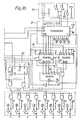
- Figure 1 represents schematically a modular, reconfigurable bus system for interrogating a number of geographically distributed data points, where each data point consists either of a single electrical contact which may be open or closed, or of an analogue transducer having its outputs converted to a digital signal. The system operates under the control of a
processor 2, which transmits interrogation signals to abus multiplexer 4, causing thebus multiplexer 4 to interrogate the status of all the data points coupled to thecommunication buses 6 having an address corresponding to the interrogation signals. The multiplexer, on receipt of the interrogation signals, reproduces the signals in an appropriate manner and transmits the modified signals to all of the single point and multiplexedtransmitters 8 where they are compared to a strapped address, A, and if a match occurs, that data point's status response signal is transmitted back to thebus multiplexer 4. Thebus multiplexer 4 then serializes the individual response signals and transmits the serial response signal to theprocessor 2 where the signal is analyzed under software control. - The present bus system can be configured in either an open or closed loop fashion, with each of the data points coupled to the
bus 6, which may be a twisted pair cable, via the single point or the multiplexedtransmitters 8, which will be described in more detail later. It is to be noted that the present embodiment is directed to an open loop system, which can accommodate up to eight buses at thebus multiplexer 4 with eachbus 6 coupled to fifteen discrete data points and each data point having a four bit strapped address, A, hardwired to its associatedtransmitter 8. It is thus possible to accommodate 120 data points if all single point transmitters are used. If the multiplexed transmitters are used, the system can accommodate 192 data points, assuming three multiplexed and three single point transmitters per input of thebus multiplexer 4. - If the system is configured as a totally closed loop, it can accommodate either 60 or 92 data points, since the
bus multiplexer 4 interrogates the same data points from each end ofbus 6. The redundant closed loop system, however, enables the detection of failure conditions, such as the severing of thebus 6. The closed loop system also requires more processor time to sort the serial response signal received from thebus multiplexer 4 for each interrogation. The present invention, however, is not directed to the operations required within theprocessor 2, since they are primarily software oriented, and merely assumes that theprocessor 2 appropriately initiates the interrogation signals and that the consequent data handling operations occur under the control ofprocessor 2, and are fixed at the time each system is configured. - The typical sequence of events that occur in the multiplexer during each interrogation cycle of the system will now be described with reference to each system element and the bus timing diagram of Figure 4. Referring also now to Figures 2, 3 and 4, as the line driver/
receiver 10 receives the serial interrogation signal from theprocessor 2, which may be a ±5 volt Baudot code corresponding to the strapped address, A, of one data point coupled to each of thebuses 6, it couples the signal to theasynchronous transceiver 12, driven by the 1.8MHz clock 14, where the signal is converted into a parallel, five bit, binary interrogation signal. Once the conversion is complete, a data ready (DR) signal is transmitted to the low speed clock enablelogic circuitry 17, which enablesfrequency divider 18 and causestransceiver 12 to clear and load the interrogation signal intocounter decoder 16, thus presetting the down count of counter/decoder 16 at a value of m. The enabling of thefrequency divider 18 causesfrequency divider 18 to disable thelogic circuitry 17 during the remainder of the interrogation cycle and load and initiate its counters such that it divides down the 1.8 MHz clock signal to produce a 7.03 KHz clock signal which is then used to clock counter/decoder 16 andpulse generator 20. It is also to be noted that the enabling offrequency divider 18 causespulse generator 20 to produce one additional pulse. As counter/decoder 16 counts down from its preset m value, it causespulse generator 20 to produce one pulse for each low speed clock cycle, approximately 140 µsec, for so long as the value in counter/decoder 16 is greater than or equal to zero. As a consequence, thebus multiplexer 4 produces a serial pulse train of m+1 pulses which is transmitted from each of the eight output ports of bus driver/receiver 22 to all the single point and multiplexedtransmitters 8 coupled to thebuses 6. - With the transmission of the last pulse during the zero count period,
counter decoder 16 continues to count down to a value ofA minus 6, which establishes a 770 µsec time period. During this time, the response pulse from each of the transmitters having the strapped address, A, corresponding to the number of pulses in the pulse train is received and transmitted to theprocessor 2. In particular, during the last half of the minus two count period, typically 28µ µsec later, counter/decoder 16 couples a transmit load, TL signal to the TL terminal oftransceiver 12 which causes the response signals from thetransmitter 8 waiting on the input ports A through J of bus driver/receiver 22 to be loaded intotransceiver 12. The response signals are loaded intransceiver 12 in parallel but during the next 490 flsec, while counter/decoder 16 counts down tominus 6, the response signals are transmitted via the line driver/receiver 10 in a serial fashion to theprocessor 2 for sorting and analysis. The 490 flsec period also enables each of thetransmitters 8 to clear prior to receipt of the next interrogation pulse train, thus preventing any spurious response pulses from being transmitted. - Prior to continuing the description of the detailed operation of the single point and multiplexed transmitters, a few design points should be noted. In particular, the least significant bit position, Ao, of the transmitter inputs are not used for address interrogation information, which dictates that m equal two times the value of the strapped address (m=2A) being interrogated. It should also be noted that, in the present system, the first pulse is not recognized by the
transmitters 8 as part of an interrogation signal, but rather is used to initiate and load thetransmitters 8 with their strapped address; thetransmitters 8 therefore respond only if they receive two times the value of their strapped address plus one pulse. Further, to interrogate fully the status of any data point associated with a single point transmitter, it is necessary to transmit two pulse trains of (m+1) and (m+2) pulses in succession, and then compare the serial response signals in theprocessor 2 according to the interpretations of Table I
receiver 22 with the response signals on each input port sequentially assigned, with A assigned the least significant bit position of the serial response signal and F assigned the most significant bit position. - Referring now to Figures 4, 5 and 6, the operation of a single point transmitter will be described. The same sequence of events occurs within each single point transmitter coupled to each of the
buses 6. Upon receipt of the first pulse from thebus multiplexer 4, thereceiver 24, which may be a Schmitt trigger, produces a noise free, square pulse which causestimer 28, which may be a retriggerable single shot, to being timing, and counter 26 to load its 4 bit strapped address, A, in complementary form, and the status input of its associated data point, which is coupled to the Ao bit position ofcounter 26. Once the Q terminal oftimer 28 goes to a logic "high",counter 26 will count up on receipt of subsequent pulses. Each subsequent pulse will cause thecounter 26 to advance andtimer 28 to reset its time to zero. The Q terminal oftimer 28 will thus remain "high" until approximately one pulse period beyond the end of the pulse train. Following the end of the pulse train, the binary signal on the terminal count, TC, terminal ofcounter 26 will correspond with the conditions established in Table II.
- When
timer 28 times out, its Q terminal goes "high" and causes the signal at the TC terminal ofcounter 26 to be stored in the D flip-flop 33, and the Q terminal goes "low" andtriggers timer 30.Timer 30, which consists of two series coupled single shots, will delay approximately one half clock pulse period, nominally 70 jUsec, and then produce an output pulse of approximately one pulse period, nominally 140,usec. If the condition of the TC terminal ofcounter 26 is "high" (i.e., 2A+1 pulses and status of 0 or 2A+2 pulses and status of 1) terminal Q of the flip-flop 33 will be "high" andline driver 32, a logical NAND circuit, will transmit a "low" response signal, over thedata bus 6 to thebus multiplexer 4. If the TC terminal is "low", a "high" response signal (i.e., the bus remains at a logic "high") will be transmitted. - If it is desired to use a single point transmitter as a data receiver rather than a data transmitter, the Q or Q terminal of the J-K flip-
flop 35 is connected to the status input and the other to the data point's input and/or a monitor station and the operation of the transmitter remains the same as during normal data transmission operations. Assuming Q is coupled to the status input, if it is desired to set flip-flop 35, a pulse train of2A+ 1 pulses is applied. If flip-flop 35 was previously set, the status on the Q terminal will be "low", the TC terminal ofcounter 26 coupled to the J and K inputs will be "low" and flip-flop 35 will remain set. If flip-flop 35 was previously cleared, the status on the Q terminal will be "high", the TC terminal ofcounter 26 will be "high" and flip-flop 35 will change state to the set condition. If it is desired to clear flip-flop 35, a pulse train of 2A+2 pulses is applied and the response will be similar to that described for setting the previously set or cleared flip-flop 35. Typically, however, the previous state of flip-flop 35 is known and the appropriate pulse train is applied to force a change of state and thereby affect the status of the data point. - Whenever a setting or clearing operation causes the flip-
flop 35 to change state, a response signal is produced identical to that produced in normal data transmitter operation. This response signal is then observed by theprocessor 2 as a confirmation of the change of state. Thus it is possible to vary the output to selected data points and monitor the operation to ensure the change. It is to be recognised that during the operation of the single point transmitters as a data receiver, all but one of the NAND gates of bus driver/receiver 22 have their inputs disabled so that only one of the data points corresponding to the pulse train is affected. - It should also be recognised that the system's single point transmitters, as well as the multiplexed transmitters, are fabricated from low power, complementary metal-oxide semiconductor (CMOS) parts which enables each
transmitter 8 to operate without a separate power supply. The transmitter, instead, derives its power from the interrogation pulse trains from thebus multiplexer 4 via theVcc generator 34 which converts part of the energy in the pulse trains to a constant Vcc voltage which is coupled to the power pins of each part. Specifically, the Vcc generator consists of a series coupled diode-capacitor combination and the Vcc voltage is the voltage that develops across the capacitor. - While many systems have widely dispersed data points, the data points may in some cases be geographically concentrated. In such circumstances, a hardware saving can be achieved with the multiplexed transmitter shown in Figures. 7 and 8 and at the same time an increase in the number of addressable data points per
bus multiplexer 4 input port and a reduction in interrogation time may be realised. The multiplexed transmitter achieves these ends by requiring fewer terminals per loop and fewer pulse trains to interrogate the data points coupled to the multiplexed transmitter. The multiplexed data points can be completely interrogated with eight pulse trains, whereas an equal number of single point transmitters requires fourteen pulse trains. - Referring now to Figures 7 and 8, a seven bit multiplexed transmitter is shown which comprises similar CMOS parts and operates in a similar fashion to the single data point transmitter previously described. The multiplexed transmitter requires four addresses to accommodate seven data points, whereas the single point transmitter required one address per data point. The seven data points are thus grouped and represented by four bit positions, but the least significant bit position of the strapped address now corresponds to a wired "high".
- A typical sequence of events will now be described with reference to the selection of the status information on status input "0" and the transmission of the corresponding response signal. When the multiplexed transmitter receives the first pulse of the (2A+ 1) pulse train,
timer 38, which may be a retriggerable single-shot, is initiated andcounter 36 is loaded with strapped address A in complementary form, thus permitting counter 36 to count on the successive pulses. Since the address being interrogated with the (2A+1 ) pulse train corresponds to the status input "0", the strapped address will match the count and the TC terminal will indicate a logic "high" at the end of the pulse train. Whentimer 38 times out, approximately one pulse period after the interrogation pulse train,timer 40 is initiated and produces a logic "high" which remains approximately one-half pulse period. The logic "high" fromcounter 36 andtimer 40 then causeregister 44 to impress the status inputs "0" through "6" of the seven discrete data points on the inputs Do to D5 and D, ofmultiplexer 46. At the same time, three bits of the count information in counter 36 (i.e., a binary 111) corresponding to status input "0" bit position inregister 44 are impressed on the select inputs Ao through A2 ofmultiplexer 46 and four bits indicating a match of the strapped address are impressed ondecoder 42, causingdecoder 42 to produce a logic "high". - Upon
timer 40 timing out, a logic "low" is produced which causestimer 48 to begin timing and produce a logic "high".NAND gate 50 responding to the logic "high's" fromtimer 48 anddecoder 42 produces a logic "low" which enablesmultiplexer 46 to select the information resident at its D, bit position which corresponds to the status input "0". - Table III shows the effects of the pulse trains of (2A+2) through (2A+8), which are used to interrogate the remaining
status bits 1 through 6, andparity bit 7. It is to be noted that register 44 is loaded only on the (2A+1 ) pulse train, since typically theprocessor 2 interrogates each strapped address sequentially. - Once the information in the status input "0" bit position is selected, it is next stored in flip-
flop 51. This occurs sincedecoder 42 produces a logic "high" on its output terminal W for each of the eight sequential pulse trains of Table III, thus astimer 48 goes "high",NAND gate 50 will causemultiplexer 46 to load flip-flop 51. If a logic "high" is present on the selected status input or parity bit position ofmultiplexer 46, flip-flop 51 will set for the duration of thetimer 48 "high" output. The resulting "high" output on the Q terminal of set flip-flop 51 will then causeline driver 52 to produce a logic "low" which will be transmitted tomultiplexer 4. In a similar manner, if flip-flop 51 is cleared, a logic "high" is transmitted.
- As the status inputs are sequentially addressed, an "odd" parity bit, associated with the D6 bit position of
multiplexer 46, is also generated in the following manner: at thetime register 44 is first loaded, the parity flip-flop 54 is cleared which indicates that an even number of "1 's" (zero at this point in time) have been transmitted. However, when a "1" is transmitted, its trailing edge, signified by the Q terminal of flip-flop 51 going "low", causes the parity flip-flop 54 to toggle (i.e., reverse status). Thus the transmission of an odd number of "ones" will leave the parity flip-flop 54 set; an even number will leave it cleared. When the parity bit is selected on the (2A+8) pulse train, the status of the Q terminal of flip-flop 54 is selected by themultiplexer 46. If an even number of "1's" has been transmitted, Q will be "high" thus transmitting an additional "1 ". If an odd number of ones has been transmitted, will be "low" and "0" will be sent. It should be noted that the processor can cause failure of the parity generation by failing to perform the interrogations in the order indicated, but the processor is considered to be "smart" enough not to do this. - The
bus multiplexer 4, on receipt of the interrogated transmitter's response signals at input ports A through F, transmits the information in the manner previously described back toprocessor 2 via theasynchronous transceiver 12 and line driver/receiver 10. Theprocessor 2, under software or firmware control, then processes the information, which activity is dependent on the configuration of the system selected from the possible permutations of transmitters on each of the open or closedloop data buses 6.
Claims (6)
Applications Claiming Priority (2)
| Application Number | Priority Date | Filing Date | Title |
|---|---|---|---|
| US06/097,080 US4360912A (en) | 1979-11-23 | 1979-11-23 | Distributed status reporting system |
| US97080 | 1993-07-22 |
Publications (2)
| Publication Number | Publication Date |
|---|---|
| EP0029705A1 EP0029705A1 (en) | 1981-06-03 |
| EP0029705B1 true EP0029705B1 (en) | 1984-10-31 |
Family
ID=22260887
Family Applications (1)
| Application Number | Title | Priority Date | Filing Date |
|---|---|---|---|
| EP80304144A Expired EP0029705B1 (en) | 1979-11-23 | 1980-11-19 | Status reporting system and data transmitters for use in such a system |
Country Status (5)
| Country | Link |
|---|---|
| US (1) | US4360912A (en) |
| EP (1) | EP0029705B1 (en) |
| JP (1) | JPS5687960A (en) |
| CA (1) | CA1157544A (en) |
| DE (1) | DE3069567D1 (en) |
Families Citing this family (18)
| Publication number | Priority date | Publication date | Assignee | Title |
|---|---|---|---|---|
| JPS57208746A (en) * | 1981-06-18 | 1982-12-21 | Toyota Motor Corp | Transmission controlling system |
| US4413258A (en) * | 1981-12-14 | 1983-11-01 | Burroughs Corporation | Interconnection for local area contention networks |
| US4472712A (en) * | 1982-03-05 | 1984-09-18 | At&T Bell Laboratories | Multipoint data communication system with local arbitration |
| JPS58198993A (en) * | 1982-05-15 | 1983-11-19 | Matsushita Electric Works Ltd | Time-division multiplex transmission system |
| JPS5952992A (en) * | 1982-09-20 | 1984-03-27 | Matsushita Electric Works Ltd | Multiplex transmission control system |
| GB2143403B (en) * | 1983-07-15 | 1986-10-29 | Standard Telephones Cables Ltd | Telecommunication exchange |
| DE3429941A1 (en) * | 1983-08-15 | 1985-05-09 | Honda Giken Kogyo K.K., Tokio/Tokyo | MULTIPLE COMMUNICATION SYSTEM FOR VEHICLE BODIES |
| US4710919A (en) * | 1983-10-21 | 1987-12-01 | International Teldata Corporation | Multiplex system for automatic meter reading |
| BE898499A (en) * | 1983-12-19 | 1984-04-16 | Rombaut Willy | Method and device for electronically transferring information. |
| JPS60231201A (en) * | 1984-04-29 | 1985-11-16 | Toshiba Corp | Sensor circut |
| GB2189333B (en) * | 1986-03-20 | 1989-11-15 | Lucas Electrical Electronics A | Vehicle condition monitoring system |
| US5109484A (en) * | 1986-04-09 | 1992-04-28 | International Business Machines Corporation | Self configuring terminal which polls loop network and generates list of connected devices for use in selectively downloading control programs |
| DE4036639A1 (en) * | 1990-11-16 | 1992-05-21 | Esser Sicherheitstechnik | METHOD FOR DETERMINING THE CONFIGURATION OF THE DETECTORS OF A DANGER DETECTION SYSTEM AND FOR DETERMINING DETECTORS SUITABLE FOR THE SYSTEM CONFIGURATION |
| JP2873515B2 (en) * | 1991-03-29 | 1999-03-24 | マツダ株式会社 | Multiplex transmission method |
| US5983371A (en) * | 1997-07-11 | 1999-11-09 | Marathon Technologies Corporation | Active failure detection |
| US6775726B2 (en) * | 2001-08-28 | 2004-08-10 | Sunrise Telecom Incorporated | Serial unit identification |
| US7443890B2 (en) * | 2002-08-12 | 2008-10-28 | Broadcom Corporation | Multi-stage multiplexing chip set having switchable forward/reverse clock relationship |
| US9306625B2 (en) | 2013-07-09 | 2016-04-05 | The Boeing Company | Systems and methods for broadband over power line multiple interface devices and systems |
Family Cites Families (13)
| Publication number | Priority date | Publication date | Assignee | Title |
|---|---|---|---|---|
| US3597549A (en) * | 1969-07-17 | 1971-08-03 | Bell Telephone Labor Inc | High speed data communication system |
| US3828313A (en) * | 1971-09-22 | 1974-08-06 | American Multiplex Syst Inc | Method and apparatus for data transmission |
| US3883693A (en) * | 1972-07-11 | 1975-05-13 | Applied Information Ind | Digital communication system |
| JPS4839895A (en) * | 1972-09-22 | 1973-06-12 | ||
| US3889064A (en) * | 1974-03-27 | 1975-06-10 | Nasa | Asynchronous, multiplexing, single line transmission and recovery data system |
| GB1478363A (en) * | 1974-07-30 | 1977-06-29 | Mullard Ltd | Data transmission systems |
| JPS51130108A (en) * | 1975-05-06 | 1976-11-12 | Tokyo Electric Power Co Inc:The | Data collection system |
| CH610167A5 (en) * | 1976-02-26 | 1979-03-30 | Vogelsang Remo | Data transmission system with stations connected to a common transmission line |
| US4093946A (en) * | 1976-03-01 | 1978-06-06 | The Laitram Corporation | Two-wire, multiple-transducer communications system |
| US4053714A (en) * | 1976-04-06 | 1977-10-11 | Canadian Pgl Electronics Inc. | Electrical data collecting device |
| GB1589748A (en) * | 1976-09-10 | 1981-05-20 | Matsushita Electric Works Ltd | Time division multiplex transmission system |
| US4089051A (en) * | 1977-01-24 | 1978-05-09 | Bell Telephone Laboratories, Incorporated | Alternative direct and indirect addressing |
| JPS55105491A (en) * | 1979-02-07 | 1980-08-13 | Nec Corp | Data exchange system |
-
1979
- 1979-11-23 US US06/097,080 patent/US4360912A/en not_active Expired - Lifetime
-
1980
- 1980-10-06 CA CA000361621A patent/CA1157544A/en not_active Expired
- 1980-11-19 EP EP80304144A patent/EP0029705B1/en not_active Expired
- 1980-11-19 DE DE8080304144T patent/DE3069567D1/en not_active Expired
- 1980-11-25 JP JP16578080A patent/JPS5687960A/en active Pending
Also Published As
| Publication number | Publication date |
|---|---|
| JPS5687960A (en) | 1981-07-17 |
| CA1157544A (en) | 1983-11-22 |
| DE3069567D1 (en) | 1984-12-06 |
| US4360912A (en) | 1982-11-23 |
| EP0029705A1 (en) | 1981-06-03 |
Similar Documents
| Publication | Publication Date | Title |
|---|---|---|
| EP0029705B1 (en) | Status reporting system and data transmitters for use in such a system | |
| US4402040A (en) | Distributed bus arbitration method and apparatus | |
| US4133504A (en) | System for protected data transmission to track-bound vehicles | |
| US3668645A (en) | Programable asynchronous data buffer having means to transmit error protected channel control signals | |
| US4298860A (en) | Monitor and control apparatus | |
| WO1985005707A1 (en) | Fault tolerant, frame synchronization for multiple processor systems | |
| US3564145A (en) | Serial loop data transmission system fault locator | |
| US5132987A (en) | Bidirectional communication line buffer apparatus | |
| US4134103A (en) | Error-rejecting data transmission system | |
| US4360918A (en) | Arrangement for detecting defects during the asynchronous transfer of digital measured values | |
| US3916123A (en) | Event monitoring transceiver | |
| US3965294A (en) | Method of and apparatus for testing transmission line carrying bipolar PCM signals | |
| US4386426A (en) | Data transmission system | |
| US3719930A (en) | One-bit data transmission system | |
| US4665477A (en) | Method for ensuring safe operation of a programmable automatic control device and automatic control device for carrying out the said method | |
| US4229819A (en) | Data transmission system | |
| US3245066A (en) | Signalling system | |
| US3427590A (en) | Priority and regular message pickup from multistation line data station transmitters | |
| US3643025A (en) | Information transmission systems | |
| SU1727112A1 (en) | Distributed system for programmed control with majorizing | |
| US3428949A (en) | Distributor system for monitoring position and status of a number of points | |
| SU1732366A1 (en) | Device for telemetry and supervisory indication | |
| SU1647876A1 (en) | Pulse duration selector | |
| SU1252780A1 (en) | System for checking complex relay distributors | |
| SU579649A1 (en) | Information compressing device |
Legal Events
| Date | Code | Title | Description |
|---|---|---|---|
| PUAI | Public reference made under article 153(3) epc to a published international application that has entered the european phase |
Free format text: ORIGINAL CODE: 0009012 |
|
| AK | Designated contracting states |
Designated state(s): DE FR GB IT |
|
| 17P | Request for examination filed |
Effective date: 19810904 |
|
| ITF | It: translation for a ep patent filed |
Owner name: ING. C. GREGORJ S.P.A. |
|
| GRAA | (expected) grant |
Free format text: ORIGINAL CODE: 0009210 |
|
| AK | Designated contracting states |
Designated state(s): DE FR GB IT |
|
| REF | Corresponds to: |
Ref document number: 3069567 Country of ref document: DE Date of ref document: 19841206 |
|
| ET | Fr: translation filed | ||
| PLBE | No opposition filed within time limit |
Free format text: ORIGINAL CODE: 0009261 |
|
| STAA | Information on the status of an ep patent application or granted ep patent |
Free format text: STATUS: NO OPPOSITION FILED WITHIN TIME LIMIT |
|
| 26N | No opposition filed | ||
| ITTA | It: last paid annual fee | ||
| PGFP | Annual fee paid to national office [announced via postgrant information from national office to epo] |
Ref country code: FR Payment date: 19931110 Year of fee payment: 14 |
|
| PGFP | Annual fee paid to national office [announced via postgrant information from national office to epo] |
Ref country code: GB Payment date: 19941017 Year of fee payment: 15 |
|
| PGFP | Annual fee paid to national office [announced via postgrant information from national office to epo] |
Ref country code: DE Payment date: 19941130 Year of fee payment: 15 |
|
| PG25 | Lapsed in a contracting state [announced via postgrant information from national office to epo] |
Ref country code: FR Effective date: 19950731 |
|
| REG | Reference to a national code |
Ref country code: FR Ref legal event code: ST |
|
| PG25 | Lapsed in a contracting state [announced via postgrant information from national office to epo] |
Ref country code: GB Effective date: 19951119 |
|
| GBPC | Gb: european patent ceased through non-payment of renewal fee |
Effective date: 19951119 |
|
| PG25 | Lapsed in a contracting state [announced via postgrant information from national office to epo] |
Ref country code: DE Effective date: 19960801 |