EP0036933A2 - Pluggable connector and its use in making a disconnectible electrical connection - Google Patents
Pluggable connector and its use in making a disconnectible electrical connection Download PDFInfo
- Publication number
- EP0036933A2 EP0036933A2 EP81100942A EP81100942A EP0036933A2 EP 0036933 A2 EP0036933 A2 EP 0036933A2 EP 81100942 A EP81100942 A EP 81100942A EP 81100942 A EP81100942 A EP 81100942A EP 0036933 A2 EP0036933 A2 EP 0036933A2
- Authority
- EP
- European Patent Office
- Prior art keywords
- elements
- contact elements
- contact
- elastic
- circuit board
- Prior art date
- Legal status (The legal status is an assumption and is not a legal conclusion. Google has not performed a legal analysis and makes no representation as to the accuracy of the status listed.)
- Withdrawn
Links
Images

Classifications
-
- H—ELECTRICITY
- H01—ELECTRIC ELEMENTS
- H01R—ELECTRICALLY-CONDUCTIVE CONNECTIONS; STRUCTURAL ASSOCIATIONS OF A PLURALITY OF MUTUALLY-INSULATED ELECTRICAL CONNECTING ELEMENTS; COUPLING DEVICES; CURRENT COLLECTORS
- H01R12/00—Structural associations of a plurality of mutually-insulated electrical connecting elements, specially adapted for printed circuits, e.g. printed circuit boards [PCB], flat or ribbon cables, or like generally planar structures, e.g. terminal strips, terminal blocks; Coupling devices specially adapted for printed circuits, flat or ribbon cables, or like generally planar structures; Terminals specially adapted for contact with, or insertion into, printed circuits, flat or ribbon cables, or like generally planar structures
- H01R12/70—Coupling devices
- H01R12/82—Coupling devices connected with low or zero insertion force
- H01R12/85—Coupling devices connected with low or zero insertion force contact pressure producing means, contacts activated after insertion of printed circuits or like structures
-
- H—ELECTRICITY
- H01—ELECTRIC ELEMENTS
- H01R—ELECTRICALLY-CONDUCTIVE CONNECTIONS; STRUCTURAL ASSOCIATIONS OF A PLURALITY OF MUTUALLY-INSULATED ELECTRICAL CONNECTING ELEMENTS; COUPLING DEVICES; CURRENT COLLECTORS
- H01R12/00—Structural associations of a plurality of mutually-insulated electrical connecting elements, specially adapted for printed circuits, e.g. printed circuit boards [PCB], flat or ribbon cables, or like generally planar structures, e.g. terminal strips, terminal blocks; Coupling devices specially adapted for printed circuits, flat or ribbon cables, or like generally planar structures; Terminals specially adapted for contact with, or insertion into, printed circuits, flat or ribbon cables, or like generally planar structures
- H01R12/70—Coupling devices
- H01R12/71—Coupling devices for rigid printing circuits or like structures
- H01R12/72—Coupling devices for rigid printing circuits or like structures coupling with the edge of the rigid printed circuits or like structures
- H01R12/721—Coupling devices for rigid printing circuits or like structures coupling with the edge of the rigid printed circuits or like structures cooperating directly with the edge of the rigid printed circuits
-
- Y—GENERAL TAGGING OF NEW TECHNOLOGICAL DEVELOPMENTS; GENERAL TAGGING OF CROSS-SECTIONAL TECHNOLOGIES SPANNING OVER SEVERAL SECTIONS OF THE IPC; TECHNICAL SUBJECTS COVERED BY FORMER USPC CROSS-REFERENCE ART COLLECTIONS [XRACs] AND DIGESTS
- Y10—TECHNICAL SUBJECTS COVERED BY FORMER USPC
- Y10T—TECHNICAL SUBJECTS COVERED BY FORMER US CLASSIFICATION
- Y10T29/00—Metal working
- Y10T29/49—Method of mechanical manufacture
- Y10T29/49002—Electrical device making
- Y10T29/49117—Conductor or circuit manufacturing
- Y10T29/49169—Assembling electrical component directly to terminal or elongated conductor
Definitions
- the invention relates to a connector for producing a releasable electrical connection between a plurality of mutually electrically insulated first contact elements and an equal number of second contact elements according to the preamble of claim 1 and the use of the connector.
- Metal springs for example made of spring bronze, serve as contact elements of the female connectors. At the same time, they fulfill the three functions of power conduction, contacting and generating the contact pressure necessary for contacting.
- the contact pressure required for perfect contacting is relatively large. In the case of longer plug strips, a total force for spreading the springs must therefore be applied when plugging in a circuit board, which is quite considerable. This force must be overcome when the circuit board is inserted by pressing the springs apart with the beveled circuit board edges.
- the circuit board material for example glass fiber reinforced epoxy resin
- the sharp edges of the conductor tracks due to the etching processes the contact surfaces of the springs wear out noticeably.
- the dimensions of the springs must be kept relatively large so that sufficient spring forces can be permanently guaranteed. This in turn prevents a reduction in the size of the connector strips or an increase in the contacts with the same size.
- zero force connectors for example from Cannon, DL series
- the contact pressure between the contact elements of the one and the other plug-in element required for contacting is generated externally by a force transmitter, for example by an eccentric, after the force-free insertion.
- the zero-force connectors are subject to minimal wear and tear and ensure a uniform contact force for all contact elements.
- the zero-force plug connectors must be accessible from two places, on the one hand for inserting the plate to be contacted and on the other hand for operating the force transmitter.
- Another disadvantage is that the contact surfaces do not or only slightly rub against each other during the production of the contact and the self-cleaning effect caused thereby is small.
- a connector is known from European patent application 0014511 (application no. 80 200 104.0), in which the contact elements only have the properties of current conduction and contacting, while the contact pressure required for contacting is applied by means of a force deflector during the insertion process.
- This force deflector is a permanently elastic element that is pressed together over profile surfaces when the circuit board to be contacted is inserted. Because of the profile surface shape, the force deflector deviates transversely to the plug-in direction and presses the one or other contact elements that are meanwhile adjacent to one another. A snap connection holds the arrangement in the pushed-together state against the restoring force of the permanently elastic element.
- the object of the invention is therefore to specify a plug connector "in which the plate to be contacted can be inserted via a plug-in opening as in a conventional female connector, but the contact elements do not exert any direct force against one another.
- the contact forces should instead be used during and by the The connector that fulfills this task is characterized by the characterizing part of the first claim.
- Claims 2 to 12 represent special embodiments.
- Claim 13 finally makes statements about the use of the connector.
- the connector thus has properties that combine the advantages of today's female connectors with the advantages of zero-force connectors. This means establishing the plug connection with a single handle, careful handling of the contact surfaces at the start of the plugging process, reduced and not suddenly changing plugging forces, sufficient grinding to ensure safe contact towards the end of the plugging process and secure mounting of the inserted plate without a complicated holding mechanism.
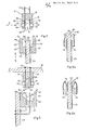
- FIG. 1 shows a perspective view of a plug connector, which is composed of a socket strip 11 and an associated, directly pluggable circuit board 23 to be contacted with the socket strip 11.
- the socket strip 11 forms a (first) carrier element for first contact elements and the printed circuit board 23 a (second) carrier element for second contact elements.
- connection pins 15 denotes a plurality of connecting pins arranged in two rows next to one another, of which only the four delimiting pins are drawn. These connection pins can be designed to connect plugged, soldered, crimped or other connections.
- Each connector pin 15 is connected to a (first) contact element in the interior of the base body 12 or forms a unit with the latter. The desired electrical connection between the connecting pins 15 and the printed conductor lines 29 of the printed circuit board 23 is established via these (first) contact elements.
- the circuit board 23 to be contacted can be inserted into the base body 12 from below via a plug-in opening 17 hidden in FIG. 1, corresponding to the position of the socket strip 11, the circuit board being guided through the plug-in opening.
- Each of the two longitudinal walls of the base body 12 has a slot opening 19 running parallel to the longitudinal edge, through which one or more elastic elements 31 protrude beyond the flat longitudinal sides 20 of the base body, which are oriented parallel to the plugging direction.
- the printed circuit board 23 carries on both sides conductor tracks 29 which, as in known, directly pluggable boards, each end in a row of parallel contact strips 30 on a projection 22 of the board 23. These contact strips 30 form the (second) contact elements of the printed circuit board. They are covered on both sides of the plate by a clamp element 37. These clamp elements are rigidly connected to the printed circuit board 23 via rivets or screws 36. During the insertion process, they slide over the elastic elements 3 1 , which - as described - protrude beyond the flat longitudinal sides 20 of the base body 12. Here, these elastic elements are pressed inwards and deformed elastically.
- Fig. 2 shows the socket strip 11 and the circuit board 23 in section transverse to their longitudinal directions.
- the designations correspond to those of Fig. L.
- the base body 12 of the socket strip 11 is hollow.
- the cavity 21 there are the already mentioned (first) contact elements 25 as an extension of the connection pins 15 in two rows. These can be individual contact lugs or combined conductors in the form of flexible, printed circuit boards, the contact surfaces facing each other and inwards.
- the contact elements 25 are weakly elastic. The elasticity serves to hold the contact elements in the rest position in the direction of the double arrow C, so that the cavity 21 is open in the width of the plug opening 17.
- the corner edges 28 of the base body 12 also help here. However, the elasticity does not serve to generate a pressing force when the printed circuit board 23 is inserted.
- 31 are elastic elements, for example elastic profile elements made of silicone rubber. They are captively stored in the suitably shaped slot openings 19 in the flat longitudinal walls of the base body 12 so that their areas 33 protrude clearly from the openings 19 over the long sides 20 and on the other hand lightly touch the (first) contact elements 25 inside the socket strip 11 .
- the circuit board 23 is designed as a conventional, two-sided, printed circuit board.
- the protrusion 22 carries - as described - the (second) contact elements 30. These are printed, parallel juxtaposed conductor lines which end at the protrusion 22. 37 are the mirror symmetry on the two sides of the circuit board 23 rigidly fastened clamp elements which have an L-shaped cross section.
- Each clamp element 37 forms, together with the associated (second) contact elements 30 and the projection 22, a U-shaped clamp.
- One leg of the clip is formed by the free area 39 of the clip element 37, the other, approximately the same length by the projection 22 with the contact strips 30 and the arc of the U through the attachment area 38 of the clip element 37.
- the open end of the clip points in the direction of insertion, which is indicated by an arrow S.
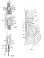
- Fig. 3 illustrates this on a larger scale.
- a (first) contact element 25 and an elastic element 31 touching it are shown, the total thickness of which is transverse to the insertion direction S has the "active thickness" D.
- D is significantly greater than the sum W of the wall thickness of the base body 12 plus the thickness of the contact element 25 or the distance of the plug opening from the outer wall.
- the clear width I transverse to the direction of insertion S between the wedge tip 41 and the (second) contact elements 30 is significantly larger than D.
- the clear width continuously decreases, becoming D at point P.
- the wedge tips 41 contactlessly touch the elastic elements 31, only touch them when the contact strips 30 lie next to the (first) contact elements 25, increasingly deform the elastic elements as the plugging process progresses, and push them across to the plugging direction S into the interior of the socket strip 11.
- the pressure on the elastic elements 31 increases, as a result of which they exert increasing pressure against the (first) contact elements 25.
- these are pressed against the contact strips 30, which rigidly absorb the pressure together with the projection 22.
- the elastic elements 31 are maximally deformed by the regions of constant internal width 43 and pressed into the interior of the socket strip 11.
- the force with which the contact surfaces of the first 25 and second 30 contact elements are pressed against one another depends on the dimensions D, I and II and the properties of the elastic elements 31.
- FIG. 4 shows some examples of cross-sectional shapes of the elastic elements 31, which are essentially in the form of strands.
- the cross section is circular, after b tubular, after c trapezoidal, after d triangular with rounded corners, after e circular, with notches at regular intervals from one side and after f such that the shape cannot be described in one word is.
- These strand-shaped profile materials are inserted into the slot openings 19 of the socket strip 11 in such a way that - as described - they protrude laterally from the flat longitudinal wall.
- the shape of the profile material is selected so that the elastic elements are held captively and essentially immovably in the slot openings 19. If an elastic element according to FIG. 4e is used, the slot openings 19 can be divided into a lattice shape, which increases the stability of the socket strip 11.
- the invention is not exhausted by this socket strip 11 and the circuit board 23 cooperating therewith. Rather, there is a significant number of other connectors that also meet the requirements mentioned.
- FIG. 5 shows a socket and a connector strip for an indirectly pluggable printed circuit board.
- 12 is in turn the basic body of the socket strip 11, the connection pins 15 of which are mechanically and electrically connected, for example, to a supporting connecting plate 16 by soldering.
- In the interior of the base body 12 there are two rows (first) contact elements 25, the contact surfaces of which point inwards, as an extension of the connecting pins 15. Slit openings 19 are again contained in the side walls, in which strand-shaped elastic elements 31 are arranged.
- the socket strip of FIG. 2 the socket strip of FIG.
- FIG. 5 shows, as a counterpart to the socket strip 11, a printed circuit board 23 to which a knife strip 47 is fastened on the side.
- This carries two rows of individual pins 48 lying side by side, the contact surfaces of which point outwards and the ones located outside the bar. Terminal ends are bent at right angles and soldered to the circuit board 23.
- the individual pins 48 are on the side of one Surround U-shaped bracket element, which forms the base body of the male connector 47. Both legs 40 of the U are chamfered on the inside and each have a wedge tip 41, a wedge area 42 and then an area adjacent to this. constant clear width 43.
- each leg 40 forms a U-shaped bracket with the associated individual pins 48.
- the clear widths 1 and II transverse to the direction of insertion are larger or smaller than the active thickness D from the sum of the thicknesses of the first contact elements 25 and the elastic elements 31 of the socket strip 11.
- the rigid counterpressure is applied by the center piece 45, on which the individual pins 48 slide along when inserted and to which they are pressed by the deformation force of the elastic elements 31.
- the middle piece 45 can be transferred from the socket strip 11 into the male connector 47, where it is arranged between the two rows of pins 48 so that it touches the pins.
- the plug-in openings 46 of the socket strip 11 combine to form a single opening, the side walls of this opening being able to have small grooves and webs, which in turn provide exact guidance of the second contact elements, i.e. of the pins 48 accomplish.
- the rigid counterpressure is applied by the middle piece combined with the pins 48.
- FIGS. 1, 2 ; 3 and 5 show variants for bracket elements,. where the properties "clamp” is combined with the additional property “exert elastic pressure”.
- the clamp elements consist of springs 53 and 54, which replace the rigid U-legs of FIGS. 1, 2 ; 3 and 5 kick.
- the other U-leg is - as described with reference to FIG. 2 - formed by the projection 22 of the circuit board 23 and the contact strips 30 located thereon.
- the U-legs, ie the springs 53 and 54 and the printed circuit board 23, are connected by rigid block pieces 55.
- the shape of the inside of the springs 53 and 54 is designed in such a way that at the open end of each U-shaped bracket there is a clear width transversely to the direction of insertion, which is greater than the active thickness D, which is defined on the basis of FIG. 3, while the more inner area has a clear width that is smaller than D.
- This pushes the open end of the U-shaped clamps does not come into contact with the elastic elements of the assigned socket strip 11 during the plugging process of the springs 53 and 54. Since these springs can be constructed with a relatively long stroke, the requirements for the mechanical tolerances can be reduced in this way.
- the round socket 80 can be fastened to a support, for example a sheet metal, by means of a flange 81.
- 82 are connection pins which end in the interior of the round socket in weakly elastic contact tabs 83, the contact surfaces of which point inwards.
- the contact lugs 83 are surrounded on the outside by a tubular, rubber-elastic elastic element 85, which is thickened like a bead at the height of the contact surfaces and which is ring-shaped and clamped at the height of the flange by the collar 86 of the flange 81.
- the circular connector 90 can be plugged together with the circular socket 80. It consists of a central, cylindrical middle part 91, which is surrounded on its circumference by second contact elements 92 running parallel to the axis. The Contact surfaces of these second contact elements 92 point outwards and the extension of the contact elements form connecting pins 94.
- the central part 91 is surrounded concentrically by a clamp element 95, which is chamfered inwards at its free end in a wedge shape. This results in a circular wedge tip -96 and a corresponding wedge area 97, to which an area 98 of constant diameter adjoins on the inside.
- the round plug 90 beaks with its middle part 91 and its wedge tip 96 without force at the start of the plugging process.
- the wedge region 97 deforms the bead of the tubular elastic element 85 and presses it inwards.
- the contact tabs 83 are pressed against the second contact elements 92.
- the region of constant diameter 98 deforms the elastic element 85 to a maximum, in such a way that no force component occurs on the circular connector 90 against the direction of insertion.
- FIG. 8 shows, as a further example of a plug connector, two identical socket strips 100 which can be plugged together.
- These carry contact elements 101 which, when pushed into one another, touch with their contact surfaces.
- the elastic elements 102 and the clamp elements 103 mutually absorb the respective counter pressure in such a way that no force component results; which could cause the two socket strips 100 to be pushed apart.
- the pushing together of the two socket strips 100 is made possible by the wedge-shaped design of the clamp elements 103, which have wedge regions 104 at their free end, which enable the two socket strips to be snapped on without force.
- Fig. 9 is a section - enlarged compared to the other figures - a section of the longitudinal wall of a female connector 11 with the slot opening 19 is shown.
- an elastic element 60 is clamped in concave recesses 58 and 59 of the side wall under slight prestress.
- the elastic element has a cross section which has the shape of an approximate oval, with which oval part 61 a comet-like linear part 62, which widens outward in a wedge shape, is homogeneously connected.
- the elastic element 60 braces with the end of the linear part 62 in the concave recess 58 and with the connecting region 70 'between the linear part 62 and the oval part 61 at the recess 59.
- the linear part 62 also closes in this way from its approximately flat outside 63 the slot opening 19 to the inside 64 of the socket strip 11 and touches the contact element 25 on the back.
- the oval part 61 protrudes with its pressure region 65 clearly beyond the outer wall 66 of the socket strip 11. Between the inside 67 of the oval part 61 and the inside 68 of the linear part 62 there is a wedge-shaped slot 69 which is open to the outside.
- the rolling movement of the oval part can be additionally secured or slipping can be avoided by designing the inner sides 67 and 68 to be toothed, so that a toothed, play-free connection is produced during the rolling movement. Accordingly, a possible sliding movement between the pressure region 65 of the oval part 61 and the clamp element 37 can be prevented by making the surface of the clamp element 37, ie the wedge region 42 and the region 43 of constant internal width slightly toothed or roughened, also matched to a corresponding one Design of the surface of the oval part 61.
- the oval part 61 rolls in the opposite direction and in turn lies against the concave recess 59 at the lower end of the slot opening 19 with slight pretension.
- the elastic element 60 can be designed such that when the oval part 61 rolls on the inside 68 of the linear part 62, the sum of the active diameter of the oval part 61 and the active width of the linear part 62 remains constant. In this case, the deformation necessary for the application of the contact force takes place by reducing the clear width of the clamp element 37. With less variation of the clear width of the clamp element 37, the production of an elastic deformation of the elastic element 60 is also possible in that by suitable shaping of the Oval part 61 and / or the linear part 62 increases the active total diameter of both parts during the rolling process.
Abstract
Es wird ein Steckverbinderprinzip angegeben mit zahlreichen speziellen Ausführungsformen. Eine Ausführungsform wird gebildet durch eine Buchsenleiste (11) und eine mit dieser zu kontaktierende Leiterplatte (23). Die Buchsenleisie trägt zwei Reihen schwach elastischer Kontaktelemente (25), deren Kontaktflächen nach innen weisen. Die Kontaktelemente werden aussen durch strangförmige Elastikelemente (31) berührt. Diese sind in Schlitzöffnungen (19) in den Längswänden der Buchsenleiste unverlierbar gelagert und ragen seitlich über die Längsseiten 20 heraus. Die Leiterplatte (23) kann mit ihren Kontaktstreifen (30), die auf einem Vorsprung (22) enden in die Oeffnung (17) der Buchsenleiste (1) eingesteckt werden. Die Leiterplatte trägt auf beiden Seiten starr mit ihr verbundene Klammerelemente (37). Diese weisen L-förmigen Querschnitt auf, und ihre Innenseiten sind keilförmig angeschrägt. Die Leiterplatte (23) und die Klammerelemente (37) schnäbeln zu Beginn des Steckvorgangs kraftfrei an. Bei weiterem Einschieben werden die Elastikelemente (31) durch die Klammerelemente (37) elastisch verformt und ins Innere der Buchsenleiste (11) gedrückt, wo sie die Kontaktelemente (25) gegen die Kontaktstreifen (30) der Leiterplatte (23) drücken. Am Ende des Steckvorgangs ergibt sich ein sicherer Stecksitz-, da aus den verformten Elastikelementen (31) keine Kraft resultiert, die entgegen der Steckrichtung (S) die selbständige Trennung der Buchsenleiste (11) und der Leiterplatte (23) bewirken könnte.A connector principle is specified with numerous special embodiments. An embodiment is formed by a socket strip (11) and a circuit board (23) to be contacted with it. The socket track carries two rows of weakly elastic contact elements (25), the contact surfaces of which point inwards. The contact elements are touched on the outside by strand-like elastic elements (31). These are captively supported in slot openings (19) in the longitudinal walls of the socket strip and protrude laterally beyond the longitudinal sides 20. The circuit board (23) with its contact strips (30), which end on a projection (22), can be inserted into the opening (17) of the socket strip (1). The circuit board carries clamp elements (37) rigidly connected to it on both sides. These have an L-shaped cross-section and their insides are bevelled. The circuit board (23) and the clamp elements (37) bite at the beginning of the plug-in process without force. When inserted further, the elastic elements (31) are elastically deformed by the clamp elements (37) and pressed into the interior of the socket strip (11), where they press the contact elements (25) against the contact strips (30) of the printed circuit board (23). At the end of the plug-in process, there is a secure plug-in seat, since no force results from the deformed elastic elements (31), which could cause the socket strip (11) and the printed circuit board (23) to separate independently against the plug-in direction (S).
Description
Die Erfindung betrifft einen Steckverbinder zur Herstellung einer lösbaren elektrischen Verbindung zwischen einer Vielzahl gegeneinander elektrisch isolierter erster Kontaktelemente und einer gleichen Zahl zweiter Kontaktelemente entsprechend dem Oberbegriff von Patentanspruch 1 sowie die Verwendung des Steckverbinders.The invention relates to a connector for producing a releasable electrical connection between a plurality of mutually electrically insulated first contact elements and an equal number of second contact elements according to the preamble of claim 1 and the use of the connector.
Steckverbinder zur Aufnahme und Kontaktierung gedruckter Leiterplatten sind in Form von Federleisten seit Jahren Stand der Technik. Als Kontaktelemente der Federleisten dienen Metallfedern, beispielsweise aus Federbronze. Sie erfüllen gleichzeitig die drei Funktionen Stromleitung, Kontaktierung und Erzeugung der zur Kontaktierung notwendigen Andruckkraft.Connectors for receiving and contacting printed circuit boards in the form of female connectors have been state of the art for years. Metal springs, for example made of spring bronze, serve as contact elements of the female connectors. At the same time, they fulfill the three functions of power conduction, contacting and generating the contact pressure necessary for contacting.
Die für eine einwandfreie Kontaktierung notwendige Andruckkraft ist relativ gross. Bei längeren Steckerleisten ist daher beim Einstecken einer Leiterplatte eine Gesamtkraft zum Spreizen der Federn aufzubringen, die recht erheblich ist. Diese Kraft muss beim Einstecken der Leiterplatte überwunden werden, indem mit den zu diesem Zweck angeschrägten Leiterplatten-Kanten die Federn auseinander gedrückt werden. Durch das Leiterplattenmaterial (beispielsweise glasfaserverstärktes Epoxydharz) und durch die durch die Aetzvorgänge scharfkantigen Leiterzug-Kanten nutzen sich hierbei die Kontaktflächen der Federn merklich ab. Weiter müssen, damit genügende Federkräfte dauerhaft gewährleistet werden können, die Dimensionen der Federn relativ gross gehalten werden. Dies wiederum verhindert eine Reduzierung der Grösse der Steckerleisten bzw. eine Vermehrung der Kontakte bei gleichbleibender Grösse.The contact pressure required for perfect contacting is relatively large. In the case of longer plug strips, a total force for spreading the springs must therefore be applied when plugging in a circuit board, which is quite considerable. This force must be overcome when the circuit board is inserted by pressing the springs apart with the beveled circuit board edges. By the circuit board material (for example glass fiber reinforced epoxy resin) and the sharp edges of the conductor tracks due to the etching processes, the contact surfaces of the springs wear out noticeably. Furthermore, the dimensions of the springs must be kept relatively large so that sufficient spring forces can be permanently guaranteed. This in turn prevents a reduction in the size of the connector strips or an increase in the contacts with the same size.
Es ist bekannt, dass bei Null-Kraft-Steckverbindern (Zero Insertion Force Connectors, beispielsweise der Fa. Cannon, DL-Serie) die Federeigenschaft der Kontaktelemente von den Kontaktierungseigenschaften getrennt sind. Die zur Kontaktierung notwendige Anpresskraft zwischen den Kontaktelementen des einen und des anderen Steckelementes wird nach dem kraftfreien Einstecken extern durch einen Kraftgeber erzeugt, beispielsweise durch einen Exzenter. Die Null-Kraft-Steckverbinder unterliegen nur geringen Verschleisserscheinungen.und gewährleisten eine gleichmässige Anpresskraft für alle Kontaktelemente. Beim heutigen engen Aufbau elektronischer Geräte ist jedoch nachteilig, dass die Null-Kraft-Steckverbinder von zwei Stellen zugänglich sein müssen, und zwar zum einen zum Einschieben der zu kontaktierenden Platte und zum zweiten zur Bedienung des Kraftgebers. Weiter ist nachteilig, dass bei der Kontaktherstellung die Kontaktflächen nicht oder nur geringfügig aufeinander schleifen und der dadurch bewirkte Selbstreinigungseffekt gering ist.It is known that in the case of zero force connectors (for example from Cannon, DL series) the spring properties of the contact elements are separated from the contacting properties. The contact pressure between the contact elements of the one and the other plug-in element required for contacting is generated externally by a force transmitter, for example by an eccentric, after the force-free insertion. The zero-force connectors are subject to minimal wear and tear and ensure a uniform contact force for all contact elements. In today's narrow structure of electronic devices, however, it is disadvantageous that the zero-force plug connectors must be accessible from two places, on the one hand for inserting the plate to be contacted and on the other hand for operating the force transmitter. Another disadvantage is that the contact surfaces do not or only slightly rub against each other during the production of the contact and the self-cleaning effect caused thereby is small.
Aus der europäischen Patentanmeldung 0014511 (Anmelde Nr. 80 200 104.0) ist ein Steckverbinder bekannt, bei dem die Kontaktelemente nur die Eigenschaften Stromleitung und Kontaktgabe aufweisen, während der für die Kontaktierung notwendige Anpressdruck mittels eines Kraftumlenkers während des Einsteckvorgangs aufgebracht wird. Dieser Kraftumlenker ist ein dauerelastisches Element, das über Profilflächen beim Einstecken der zu kontaktierenden Leiterplatte zusammengepresst wird. Aufgrund der Profilflächenform weicht der Kraftumlenker quer zur Steckrichtung aus und drückt dabei die mittlerweile nebeneinander liegenden einen und anderen miteinander zu kontaktierenden Kontaktelemente gegeneinander. Eine Rastverbindung hält die Anordnung im zusammengeschobenen Zustand gegen die Rückstellkraft des dauerelastischen Elements fest.A connector is known from European patent application 0014511 (application no. 80 200 104.0), in which the contact elements only have the properties of current conduction and contacting, while the contact pressure required for contacting is applied by means of a force deflector during the insertion process. This force deflector is a permanently elastic element that is pressed together over profile surfaces when the circuit board to be contacted is inserted. Because of the profile surface shape, the force deflector deviates transversely to the plug-in direction and presses the one or other contact elements that are meanwhile adjacent to one another. A snap connection holds the arrangement in the pushed-together state against the restoring force of the permanently elastic element.
Beim oben genannten Steckverbinder wird die Andruckkraft zur Erzeugung einwandfreier Kontakte wie beim Einstecken herkömmlicher Leiterplatten in konventionelle Federleisten im gleichen Arbeitsschritt mit dem Einschieben aufgebracht. Dies ist ein wesentlicher Vorteil gegenüber den beschriebenen Null-Kraft-Steckverbindern. Nachteilig an der Anordnung ist jedoch, dass im eingeschobenen Zustand dauernd eine Kraft wirkt, die versucht, die Leiterplatte entgegen der Steckrichtung aus dem Steckverbinder wieder herauszudrücken. Dies wird zwar durch die genannte Rastverbindung verhindert. Diese Rastverbindung ist jedoch relativ kompliziert, da der verfügbare Weg, beispielsweise für eine Ueberhubbewegung zur Ermöglichung gewollten Herausziehens, knapp ist.In the case of the connector mentioned above, the pressing force for producing perfect contacts, as when inserting conventional printed circuit boards into conventional female connectors, is applied in the same step with the insertion. This is a significant advantage over the zero-force connectors described. A disadvantage of the arrangement, however, is that, in the inserted state, a force is constantly acting which tries to push the circuit board out of the plug connector against the plugging direction. This is prevented by the mentioned locking connection. However, this latching connection is relatively complicated, since the available path, for example for an overstroke movement to enable intentional pulling out, is scarce.
Die Aufgabe der Erfindung ist es daher, einen Steckverbinder" anzugeben, bei dem die zu kontaktierende Platte wie in eine konventionelle Federleiste über eine Stecköffnung einsteckbar ist, wobei die Kontaktelemente jedoch keine direkte Kraft. gegeneinander ausüben. Die Kontaktkräfte sollen statt dessen während und durch den Steckvorgang aufgebracht werden, wobei im eingeschobenen Zustand keine Kräfte resultieren, die entgegen der Steckrichtung wirken. Der Steckverbinder, der diese Aufgabe erfüllt, ist durch den kennzeichnenden Teil des ersten Patentanspruchs gekennzeichnet. Die Ansprüche 2 bis 12 geben spezielle Ausführungsformen wieder. Der Anspruch 13 schliesslich macht Aussagen über die Verwendung des Steckverbinders.The object of the invention is therefore to specify a plug connector "in which the plate to be contacted can be inserted via a plug-in opening as in a conventional female connector, but the contact elements do not exert any direct force against one another. The contact forces should instead be used during and by the The connector that fulfills this task is characterized by the characterizing part of the first claim. Claims 2 to 12 represent special embodiments.
Der Steckverbinder besitzt damit Eigenschaften, die die Vorteile heutiger Federleisten mit den Vorteilen der Null-Kraft-Steckverbinder kombinieren. Dies bedeutet Herstellung der Steckverbindung durch einen einzigen Handgriff, schonende Behandlung der Kontaktflächen bei Beginn des Steckvorgangs, reduzierte und sich nicht sprunghaft ändernde Steckkräfte, ausreichendes Schleifen zur Gewährleistung sicherer Kontaktgabe gegen Ende des Steckvorgangs und sichere Halterung der eingesteckten Platte ohne komplizierten Haltemechanismus.The connector thus has properties that combine the advantages of today's female connectors with the advantages of zero-force connectors. This means establishing the plug connection with a single handle, careful handling of the contact surfaces at the start of the plugging process, reduced and not suddenly changing plugging forces, sufficient grinding to ensure safe contact towards the end of the plugging process and secure mounting of the inserted plate without a complicated holding mechanism.
Im folgenden wird die Erfindung anhand von Figuren beispielsweise näher beschrieben. Es zeigen:
- Fig. 1 Perspektivische Darstellung einer Buchsenleiste und einer zugeordneten, direkt steckbaren Leiterplatte
- Fig. 2 Schnitt durch die Buchsenleiste und durch die zugeordnete, direkt steckbare Leiterplatte
- Fig. 3 Schemadarstellung eines Steckverbinders mit Vermassungen (in vergrössertem Massstab)
- Fig. 4 Querschnittformen für verschiedene Elastikelemente
- Fig. 5 Schnitt durch eine zweite Buchsenleiste und eine zugeordnete, indirekt steckbare Leiterplatte
- Fig. 6a' Schnitt durch eine direkt steckbare Leiterplatte mit elastischen Klammerelementen
- Fig. 6b Schnitt durch eine zweite direkt steckbare Leiterplatte mit anderen elastischen Klammerelementen
- Fig. 7 Schnitt durch eine Rundbuchse und einen zugeordneten Rundstecker
- Fig. 8 Schnitt durch zwei ineinandersteckbare, identische Buchsenleisten
- Fig. 9 Schnitt durch die Seitenwand einer Buchsenleiste.und ein Elastikelement (in vergrössertem Massstab)
- Fig. 10 verschiedene Kombinationen von Kontaktelementen und Elastikelementen.
- Fig. 1 perspective view of a socket strip and an associated, directly pluggable circuit board
- Fig. 2 section through the socket strip and through the associated, directly pluggable circuit board
- 3 schematic representation of a connector with dimensions (on an enlarged scale)
- Fig. 4 cross-sectional shapes for different elastic elements
- Fig. 5 section through a second female header and an associated, indirectly pluggable circuit board
- Fig. 6a ' section through a directly pluggable circuit board with elastic clamp elements
- Fig. 6b section through a second directly pluggable circuit board with other elastic clamp elements
- Fig. 7 section through a round socket and an associated round plug
- Fig. 8 section through two mutually pluggable, identical socket strips
- Fig. 9 section through the side wall of a socket strip. And an elastic element (on an enlarged scale)
- Fig. 10 different combinations of contact elements and elastic elements.
Die Fig. 1 stellt in perspektivischer Darstellung einen Steckverbinder dar, der sich aus einer Buchsenleiste 11 und aus einer zugeordneten, direkt steckbaren, mit der Buchsenleiste 11 zu kontaktierenden Leiterplatte 23 zusammensetzt. Die Buchsenleiste 11 bildet dabei ein (erstes) Trägerelement für erste Kontaktelemente und die Leiterplatte 23 ein (zweites) Trägerelement für zweite Kontaktelemente.1 shows a perspective view of a plug connector, which is composed of a
12 ist der Grundkörper der Buchsenleiste 11, die über Befestigungslappen 13 und Befestigungslöcher 14 an einem Rahmen oder einer Verdrahtungsleiterplatte befestigbar ist. 15 bezeichnet eine Vielzahl, in zwei Reihen nebeneinander angeordneter Anschluss-Stifte, von denen nur die vier begrenzenden Stifte gezeichnet sind. Diese Anschluss-Stifte können ausgebildet sein zum Anschluss gesteckter, gelöteter, gecrimpter oder sonstiger Anschlüsse. Jeder Anschluss-Stift 15 ist im Innern des Grundkörpers 12 mit einem (ersten) Kontaktelement verbunden oder bildet mit diesem eine Einheit. Ueber diese (ersten) Kontaktelemente wird die gewünschte elektrische Verbindung zwischen den Anschluss-Stiften 15 und den gedruckten Leiterzügen 29 der Leiterplatte 23 hergestellt. Die zu kontaktierende Leiterplatte 23 kann zu diesem Zweck, entsprechend der gezeichneten Lage der Buchsenleiste 11, von unten über eine in Fig. 1 verdeckte Stecköffnung 17 in den Grundkörper 12 eingeschoben werden, wobei die Leiterplatte durch die Stecköffnung geführt wird.12 is the basic body of the
Jede der beiden Längswände des Grundkörpers 12 weist eine parallel zur Längskante verlaufende Schlitzöffnung 19 auf, durch die ein oder mehrere Elastikelemente 31 über die ebenen, parallel zur Steckrichtung ausgerichteten Längsseiten 20 des Grundkörpers herausragen.Each of the two longitudinal walls of the
Die Leiterplatte 23 trägt auf ihren beiden Seiten Leiterzüge29, die wie bei bekannten, direkt steckbaren Platten in je einer Reihe paralleler Kontaktstreifen 30 an einem Vorsprung 22 der Platte 23 enden. Diese Kontaktstreifen 30 bilden die (zweiten) Kontaktelemente der Leiterplatte. Sie werden auf beiden Plattenseiten durch je ein Klammerelement 37 überdeckt. Diese Klammerelemente sind mit der Leiterplatte 23 über Nieten oder Schrauben 36 starr verbunden. Sie schieben sich beim Einsteckvorgang über die Elastikelemente 31, die - wie beschrieben - über die ebenen längsseiten 20 des Grundkörpers 12 herausragen. Hierbei werden diese Elastikelemente nach innen gedrückt und elastisch verformt.The printed
Die Fig. 2 zeigt die Buchsenleiste 11 und die Leiterplatte 23 im Schnitt quer zu deren Längsrichtungen. Die Bezeichnungen entsprechen denen von Fig. l. Der Grundkörper 12 der Buchsenleiste 11 ist hohl. In der Höhlung 21 befinden sich in zwei Reihen die bereits erwähnten (ersten) Kontaktelemente 25 als Verlängerung der Anschluss-Stifte 15. Es können dies einzelne Kontaktfahnen sein oder zusammengefasste Leiter in Form von flexiblen, gedruckten Leiterplatten, wobei die Kontaktflächen gegeneinander und nach innen weisen. Die Kontaktelemente 25 sind schwach elastisch. Die Elastizität dient dazu, die Kontaktelemente in Richtung des Doppelpfeiles C in einer Ruhelage zu halten, so dass die Höhlung 21 in Breite der Stecköffnung 17 offen ist. Hierbei helfen auch die Eckkanten 28 des Grundkörpers 12 mit. Die Elastizität dient jedoch nicht dazu, bei eingeschobener Leiterplatte 23 eine Andruckkraft zu erzeugen.Fig. 2 shows the
17 ist die Stecköffnung, durch die die Leiterplatte 23 mit ihren (zweiten) Kontaktelementen 30 sauber geführt, jedoch ohne Kraftaufwendung in die Höhlung 21 einschiebbar ist. 31 sind Elastikelemente, beispielsweise elastische Profilelemente aus Siliconkautschuk. Sie sind unverlierbar in den geeignet ausgeformten Schlitzöffnungen 19 in den ebenen Längswänden des Grundkörpers 12 so gelagert, dass sie mit ihren Bereichen 33 deutlich aus den Oeffnungen 19 über die Längsseiten 20 ragen und andererseits die (ersten) Kontaktelemente 25 im Innern der Buchsenleiste 11 leicht berühren.17 is the plug-in opening through which the printed
Die Leiterplatte 23 ist als konventionelle, zweiseitige, gedruckte Leiterplatte ausgebildet. Der Vorsprung 22 trägt - wie beschrieben - die (zweiten) Kontaktelemente 30. Diese sind gedruckte, parallel nebeneinanderliegende Leiterzüge, die am Vorsprung 22 enden. 37 sind die spiegelsymmetrisch auf den beiden Seiten der Leiterplatte 23 starr befestigten Klammerelemente, die L-förmigen Querschnitt aufweisen.The
Jedes Klammerelement 37 bildet zusammen mit den zugeordneten (zweiten) Kontaktelementen 30 und dem Vorsprung 22 eine U-förmige Klammer. Der eine Schenkel der Klammer wird dabei durch den freien Bereich 39 des Klammerelements 37 gebildet, der andere, etwa gleich lange Schenkel durch den Vorsprung 22 mit den Kontaktstreifen 30 und der Bogen des U's durch den Befestigungsbereich 38 des Klammerelements 37. Das offene Ende der Klammer weist in die Steckrichtung, die durch einen Pfeil S bezeichnet ist.Each
Die nach innen weisenden Seiten der die U-Schenkel bildenden Bereiche 39 der Klammerelemente 37 sind keilförmig angeschrägt. Hierdurch ergeben sich Keilspitzen 41, Keilbereiche 42, die etwa in der Mitte der Schenkel enden und hieran anschliessend in Richtung auf den Bogen des U's Bereiche konstanter.lichter Weite 43. In diesen Bereichen 43 ist die lichte Weite zwischen den (zweiten) Kontaktelementen 30 und den Schenkeln der Klammerelemente quer zur Steckrichtung konstant.The inward-facing sides of the
Fig. 3 verdeutlicht dieses im grösseren Massstab. In der Figur oben wird ein (erstes) Kontaktelement 25 und ein dieses berührendes Elastikelement 31 gezeigt, deren Gesamtdicke quer zur Steckrichtung S die "aktive Dicke" D aufweist. D ist dabei deutlich grösser als die Summe W aus der Wandstärke des Grundkörpers 12 plus der Dicke des Kontaktelements 25 bzw. dem Abstand der Stecköffnung von der Aussenwand. Die lichte Weite I quer zur Steckrichtung S zwischen der Keilspitze 41 und den (zweiten) Kontaktelementen 30 ist deutlich grösser als D. Im Keilbereich 42 verringert sich die lichte Weite kontinuierlich, wobei sie im Punkt P gleich D wird. Der Keilbereich endet schliesslich im Bereich konstanter lichter Weite 43, indem die. lichte Weite II etwa konstant und kleiner als D aber grösser als W ist (W < II < D < I).Fig. 3 illustrates this on a larger scale. In the figure above, a (first)
Hierdurch schieben sich beim Zusammenstecken der Leiterplatte 23 und der Buchsenleiste 11 die Keilspitzen 41 berührungslos über die Elastikelemente 31, berühren diese erst dann, wenn die Kontaktstreifen 30 neben den (ersten) Kontaktelementen 25 liegen, verformen die Elastikelemente bei fortschreitendem Steckvorgang zunehmend und drücken sie quer zur Steckrichtung S in das Innere der Buchsenleiste 11. Im Laufe des Steckvorgangs erhöht sich auf diese Weise der Druck auf die Elastikelemente 31, wodurch diese einen wachsenden Druck gegen die (ersten) Kontaktelemente 25 ausüben. Hierdurch werden diese gegen die Kontaktstreifen 30 gedrückt, die den Druck zusammen mit dem Vorsprung 22 starr aufnehmen. Bei vollständig eingeschobener Leiterplatte 23 werden die Elastikelemente 31 durch die Bereiche konstanter lichter Weite 43 maximal verformt und in das Innere der Buchsenleiste 11 gedrückt. Aufgrund der-gewählten Geometrie ergibt sich hierbei keine auf die Leiterplatte 23 wirkende Kraftkomponente entgegen der Einschieberichtung S. Durch Anbringen von leichten Abschrägungen umgekehrt zu den Richtungen der Keilbereiche 42 ist es sogar möglich, eine kleine Kraftkomponente in Einschieberichtung S wirken zu lassen. Durch diese Kraft und durch die Reibungskräfte wird die Leiterplatte 23 sicher in der Buchsenleiste 11 gehalten.As a result, when the printed
Die Kraft, mit der die Kontaktflächen der ersten 25 und zweiten 30 Kontaktelemente gegeneinander gedrückt werden, ist abhängig von den Dimensionen D, I und II sowie den Eigenschaften der Elastikelemente 31. Durch das Zusammenwirken der Elastikelemente 31 der Buchsenleiste 11 und der U-förmigen Klammern der Leiterplatte 23 ergibt sich beim Steckvorgang zuerst ein kraftfreies Anschnäbeln. Anschliessend muss eine gleichmässig ansteigende, der Einsteckkraft entgegenwirkende elastische Kraft überwunden werden, wobei die ersten und zweiten Kontaktelemente gegeneinander gedrückt werden. Gegen Ende des Einsteckvorgangs ergibt sich schliesslich eine stark reduzierte Einschiebekraft, die nur die Reibungskräfte zwischen den Innenseiten der Schenkel 39 und den zugeordneten Elastikelementen 31 sowie zwischen den zu kontaktierenden ersten 25 und zweiten 30 Kontaktelementen zu überwinden hat.The force with which the contact surfaces of the first 25 and second 30 contact elements are pressed against one another depends on the dimensions D, I and II and the properties of the
Fig. 4 zeigt einige Beispiele für Querschnittformen der im wesentlichen strangförmig ausgebildeten Elastikelemente 31. Nach a ist der Querschnitt kreisförmig, nach b schlauchförmig, nach c trapezförmig, nach d dreieckförmig mit abgerundeten Ecken, nach e kreisförmig, wobei in regelmässigen Abständen von einer Seite her Einkerbungen angebracht sind und nach f derart, dass die Form nicht mit einem Wort beschreibbar ist. Diese strangförmigen Profilmaterialien sind in die Schlitzöffnungen 19 der Buchsenleiste 11 so eingelegt, dass sie - wie beschrieben - seitlich aus der ebenen Längswand herausragen. Die Formgebung des Profilmaterials ist dabei so gewählt, dass die Elastikelemente unverlierbar und im wesentlichen unverrückbar in den Schlitzöffnungen 19 gehalten werden. Bei Verwendung eines Elastikelementes nach Fig. 4e können die Schlitzöffnungen 19 gitterförmig unterteilt sein, wodurch sich die Stabilität der Buchsenleiste 11 erhöht.4 shows some examples of cross-sectional shapes of the
Die anhand der Fig. 1 bis 4 beispielsweise beschriebene Buchsenleiste 11 erfüllt im Zusammenwirken mit der Leiterplatte 23 und den Klammerelementen 37 die eingangs erwähnten Forderungen'für einen Steckverbinder, der trotz kraftlosen Anschnäbelns durch und während des Einsteckvorgangs die für die Kontaktierung notwendige Andruckkraft aufbringt, wobei im zusammengesteckten Zustand keine Kraft resultiert, die diesen Zustand aufzuheben bestrebt ist. Durch diese Buchsenleiste 11 und die damit zusammenwirkende Leiterplatte 23 ist die Erfindung jedoch nicht erschöpft. Es gibt vielmehr eine erhebliche Anzahl anderer Steckverbinder, die den genannten Forderungen ebenfalls genügen.The
Als zweites 'Beispiel eines entsprechenden Steckverbinders zeigt die Fig. 5 eine Buchsen- und eine Steckerleiste für eine indirekt steckbare Leiterplatte. 12 ist wiederum der Grundkörper der Buchsenleiste 11, deren Anschluss-Stifte 15 beispielsweise mit einer tragenden Verbindungsplatte 16 durch Verlöten mechanisch und elektrisch verbunden sind. Im Inneren des Grundkörpers 12 befinden sich als Verlängerung der Anschluss-Stifte 15 zwei Reihen (erster) Kontaktelemente 25, deren Kontaktflächen nach innen weisen. In den Seitenwänden sind wiederum Schlitzöffnungen 19 enthalten, in denen strangförmige Elastikelemente 31 angeordnet sind. Im Gegensatz zur Buchsenleiste von Fig. 2 weist die Buchsenleiste von Fig. 5 im Innern ein stegförmiges Mittelstück 45 auf, durch welches für die aufzunehmenden zweiten Kontaktelemente, die als freie Stifte 48 ausgebildet sind, einzelne Führungen bzw. Aufnahmeöffnungen 46 gebildet werden. Durch diese Führungen wird eine einwandfreie elektrische Trennung sowohl der ersten 25 wie auch der mit diesen zu kontaktierenden zweiten Kontaktelemente.. 48 untereinander gewährleistet.As a second example of a corresponding connector, FIG. 5 shows a socket and a connector strip for an indirectly pluggable printed circuit board. 12 is in turn the basic body of the
Der untere Teil von Fig. 5 zeigt als Gegenstück zur Buchsenleiste 11 eine Leiterplatte 23, an der seitlich eine Messerleiste 47 befestigt ist. Diese trägt zwei Reihen nebeneinanderliegender Einzelstifte 48, deren Kontaktflächen nach aussen weisen und deren ausserhalb der Leiste liegende. Anschlussenden rechtwinklig abgebogen und mit der Leiterplatte 23 verlötet sind. Die Einzelstifte 48 sind seitlich von einem U-förmigen Klammerelement umgeben, welches den Grundkörper der Messerleiste 47 bildet. Beide Schenkel 40 des U's sind innen abgeschrägt und besitzen je eine Keilspitze 41, einen Keilbereich 42 und anschliessend an diesen einen Bereich. konstanter lichter Weite 43.The lower part of FIG. 5 shows, as a counterpart to the
Entsprechend Fig. 2 und 3 bildet jeder Schenkel 40 mit den zugeordneten Einzelstiften 48 eine U-förmige Klammer. Die lichten Weiten 1 und II quer zur Steckrichtung sind grösser bzw. kleiner als die aktive Dicke D aus der Summe der Dicken der ersten Kontaktelemente 25 und der Elastikelemente 31 der Buchsenleiste 11. Der starre Gegendruck wird durch das Mittelstück 45 aufgebracht, an dem die Einzelstifte 48 beim Einstecken entlanggleiten und an die sie durch die Verformungskraft der Elastikelemente 31 angedrückt werden.2 and 3, each
Als Variante kann das Mittelstück 45 aus der Buchsenleiste 11 in die Messerleiste 47 übertragen werden, wo es zwischen den beiden Stiftreihen 48 so angeordnet wird, dass es die Stifte berührt. Die Stecköffnungen 46 der Buchsenleiste 11 vereinigen sich dabei zu einer einzigen Oeffnung, wobei die Seitenwände dieser Oeffnung kleine Nuten und Stege aufweisen können, die wiederum eine exakte Führung der zweiten Kontaktelemente, d.h. der Stifte 48 bewerkstelligen. Der starre Gegendruck wird in diesem Fall von dem mit den Stiften 48 vereinigten Mittelstück aufgebracht.As a variant, the
Der Vorteil einer indirekt gesteckten Leiterplatte gegenüber einer direkt gesteckten Platte besteht wie bei konventionellen Platten darin, dass alle Kontaktelemente sauber geführt und einwandfrei gegeneinander isoliert sind. Dadurch entfällt die Gefahr, dass bei schrägem Einstecken benachbarte erste Kontaktelemente 25 über die ungenau positionierten zweiten Kontaktelemente 30 fehlerhaft miteinander verbunden werden.The advantage of an indirectly inserted circuit board compared to a directly inserted board, as with conventional boards, is that all contact elements are properly guided and perfectly insulated from each other. This eliminates the risk of adjacent
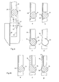
Die Figuren 6a und 6b zeigen Varianten für Klammerelemente, . bei denen die Eigenschaften "klammern" mit der zusätzlichen Eigenschaft "elastischen Druck ausüben" kombiniert ist. Die Klammerelemente bestehen in beiden-Fällen aus Federn 53 bzw. 54, die an die Stelle der starren U-Schenkel der Figuren 1, 2; 3 und 5 treten. Der andere U-Schenkel wird - wie entsprechend anhand von Fig. 2 beschrieben - durch den Vorsprung 22 der Leiterplatte 23 und die darauf befindlichen Kontaktstreifen 30 gebildet. Verbunden sind die U-Schenkel, d.h. die Federn 53 bzw. 54 und die Leiterplatte 23, durch starre Blockstücke 55.Figures 6a and 6b show variants for bracket elements,. where the properties "clamp" is combined with the additional property "exert elastic pressure". In both cases, the clamp elements consist of
Die Form der Innenseite der Federn 53 bzw. 54 ist so ausgebildet, dass sich am offenen Ende jeder U-förmigen Klammer eine lichte Weite quer zur Steckrichtung ergibt, die grösser ist als die aktive Dicke D, die anhand von Fig. 3 definiert ist, während der weiter innenliegende Bereich eine lichte Weite aufweist, die kleiner ist als D. Hierdurch schiebt sich beim Steckvorgang das offene Ende der U-förmigen Klammern berührungslos über die Elastikelemente der zugeordneten Buchsenleiste 11. Der für die Kontaktierung notwendige Anpressdruck wird im eingesteckten Zustand nicht ausschliesslich durch die Verformung der Eleastikelemente 31 (Fig. 2) aufgebracht, sondern zusätzlich durch die Federkräfte der Federn 53 bzw. 54. Da diese Federn relativ langhubig ausbildbar sind, lassen sich auf diese Weise die Anforderungen an die mechanischen Toleranzen vermindern.The shape of the inside of the
Als weiteres Beispiel für einen Steckverbinder zeigt Fig. 7, eine Rundbuchse 80 und einen zugeordneten Rundstecker 90. Die Rundbuchse 80 ist mittels eines Flansches 81 an einem Träger, beispielsweise einem Blech befestigbar. 82 sind Anschluss-Stifte, die im Inneren der Rundbuchse in schwach elastische Kontaktfahnen 83 auslaufen, deren Kontaktflächen nach innen weisen. Die Kontaktfahnen 83 sind aussen von einem rohrförmigen, gummielastischen Elastikelement 85 umgeben, welches in der Höhe der Kontaktflächen wulstartig verdickt ist und das in der Höhe des Flansches durch den Kragen 86 des Flansches 81 ringförmig umgeben und eingespannt ist.7 shows a
Zusammensteckbar mit der Rundbuchse 80 ist der Rundstecker 90. Dieser besteht aus einem zentralen, zylinderförmigen Mittelteil 91, welches auf seinem Umfang durch parallel zur Achse verlaufende zweite Kontaktelemente 92 umgeben ist. Die Kontaktflächen dieser zweiten Kontaktelemente 92 weisen nach aussen und die Verlängerung der Kontaktelemente bilden Anschluss-Stifte 94. Das Mittelteil 91 wird konzentrisch durch ein Klammerelement 95 umgeben, das an seinem freien Ende nach innen keilförmig angeschrägt ist. Hierdurch ergeben sich eine kreisförmige Keilspitze -96 und ein entsprechender Keilbereich 97, an den sich nach innen ein Bereich 98 konstanten Durchmessers anschliesst.The
Der Rundstecker 90 schnäbelt bei Beginn des Steckvorganges mit seinem Mittelteil 91 und seiner Keilspitze 96 kraftfrei an. Bei fortschreitendem Einschieben verformt der Keilbereich 97 den Wulst des schlauchförmigen Elastikelements 85 und drückt ihn nach innen. Hierbei werden die Kontaktfahnen 83 gegen die zweiten Kontaktelemente 92 gedrückt. Am Ende des Einschiebevorgangs schliesslich verformt der Bereich konstanten Durchmessers 98 das Elastikelement 85 maximal, und zwar so, dass keine Kraftkomponente auf den Rundstecker 90 entgegen der Einschieberichtung auftritt.The
Fig. 8 zeigt als weiteres Beispiel für einen Steckverbinder zwei zusammensteckbare, identische Buchsenleisten 100. Diese tragen Kontaktelemente 101, die sich im ineinander geschobenen Zustand mit ihren Kontaktflächen berühren. Auf den von den Kontaktflächen abgekehrten Seiten der Kontaktelemente befindet sich in jeder Buchsenleiste ein strangförmiges Elastikelement 102, welches durch ein Klammerelement 103 der jeweils anderen Buchsenleiste 100 gegen die Kontaktelemente 101 gedrückt wird. Hierbei nehmen die Elastikelemente 102 und die Klammerelemente 103 gegenseitig den jeweiligen Gegendruck derart auf, dass keine Kraftkomponente resultiert; die ein Auseinanderschieben der beiden Buchsenleisten 100 bewirken könnte. Das Zusammenschieben der beiden Buchsenleisten 100 wird ermöglicht durch die keilförmige Ausbildung der Klammerelemente 103, die an ihrem freien Ende Keilbereiche 104 aufweisen, die ein kraftfreies Anschnäbeln der beiden Buchsenleisten ermöglichen.FIG. 8 shows, as a further example of a plug connector, two identical socket strips 100 which can be plugged together. These carry
Beim Zusammenschieben der'bisher beschriebenen Steckverbinder, gleiten die Innenflächen der Klammerelemente, d.h. die Keilbereiche (42, 97, 104) und die Bereiche konstanter lichter Weite (43) bzw. konstanten Durchmessers (98) über die zugeordneten Elastikelemente hinweg. Hierbei werden letztere auch in Steckrichtung verformt und mechanisch abgenutzt. Eine Verbesserung der Steckverbinder ergibt sich daher dann, wenn die gewollte Verformung quer zur Steckrichtung nicht mittels eines Gleitvorgangs erzwungen wird, sondern wenn sich die Verformung während einer Rollbewegung ergibt. Fig. 9 zeigt hierfür ein Beispiel.When the connectors described so far are pushed together, the inner surfaces of the clamp elements slide, i.e. the wedge areas (42, 97, 104) and the areas of constant internal width (43) or constant diameter (98) across the assigned elastic elements. The latter are also deformed in the direction of insertion and mechanically worn. An improvement in the plug connector therefore arises if the desired deformation transverse to the plug direction is not forced by means of a sliding process, but if the deformation occurs during a rolling movement. 9 shows an example of this.
In Fig. 9 ist im Schnitt - gegenüber den anderen Figuren vergrössert - ein Ausschnitt aus der Längswand einer Buchsenleiste 11 mit der Schlitzöffnung 19 dargestellt. In dieser Schlitzöffnung ist unter leichter Vorspannung ein Elastikelement 60 in konkaven Aussparungen 58 und 59 der Seitenwand eingespannt. Das Elastikelement weist einen Querschnitt auf, der die Form eines angenäherten Ovals hat, mit welchem Ovalteil 61 ein kometenschweifartiger, sich nach aussen keilförmig erweiternder Linearteil 62 homogen verbunden ist. Im Ruhezustand, d.h. bei unbestückter Buchsenleiste 11,verspannt sich das Elastikelement 60 mit dem Ende des Linearteils 62 in der konkaven Aussparung 58 und mit dem Verbindungsbereich 70 'zwischen Linearteil 62 und Ovalteil 61 an der Aussparung 59. Der Linearteil 62 schliesst auf diese Weise mit seiner etwa ebenen Aussenseite 63 die Schlitzöffnung 19 zur Innenseite 64 der Buchsenleiste 11 ab und berührt das Kontaktelement 25 an dessen Rückseite. Das Ovalteil 61 ragt dagegen mit seinem Druckbereich 65 deutlich über die Aussenwand 66 der Buchsenleiste 11 heraus. Zwischen der Innenseite 67 des Ovalteils 61 und der Innenseite 68 des Linearteils 62 liegt dabei ein keilförmiger Schlitz 69, der nach aussen offen ist.In Fig. 9 is a section - enlarged compared to the other figures - a section of the longitudinal wall of a
Schiebt sich während eines Steckvorgangs der Keilbereich 42 eines Klammerelements 37 in Richtung des Pfeils S über den nach aussen ragenden Druckbereich 65 des Ovalteils 61, so wird aufgrund der gegebenen Geometrie und der daraus resultierenden Kraftkomponenten sowie den hierauf beruhenden Reibungskräften dieser Druckbereich 65 in Richtung des Pfeils S mitgenommen, während der Verbindungsbereich 70 zwischen dem Ovalteil 61 und dem Linearteil 62 wegen der geometrischen Anordnung und der Steifigkeit des Linearteils 62 in Richtung des Pfeiles S die genannte Bewegung nicht mitmachen kann. Hieraus entwickelt sich eine Rollbewegung des Ovalteils 61, bei der dieses mit seiner Innenseite 67 auf der Innenseite 68 des Linearteils62 abrollt, und bei der das Linearteil 62 mit seinem schmalen Ende, anschliessend an den Verbindungsbereich 70, auf das Ovalteil 61 aufgewickelt wird. Bei dieser Bewegung wird zwangsläufig der keilförmige Schlitz 69 zunehmend geschlossen. Gleichzeitig drückt das Klammerelement 37 mit seinem Keilbereich 42 oder bei fortgeschrittenem Einschieben mit seinem Bereich konstanter lichter Weite 43 auf das Ovalteil 61, wodurch dieses einschliesslich Teilen des Linearteils 62 quer zur Bewegungsrichtung S elastisch verformt und in das Innere der Buchsenleiste 11 gedrückt wird. Diese Ausweichbewegung kann durch Schlitze 71 erleichtert werden, die quer zur Längsrichtung des Linearteils 62, ausgehend von dessen Innenseite 68,im Linearteil angebracht sind. Weiter kann die Rollbewegung des Ovalteils dadurch zusätzlich gesichert bzw. ein Rutschen vermieden werden, indem die Innenseiten 67 und 68, aufeinander abgestimmt, gezahnt ausgebildet werden, so dass bei der Rollbewegung eine verzahnte, spielfreie Verbindung entsteht. Entsprechend kann eine eventuelle Gleitbewegung zwischen dem Druckbereich 65 des Ovalteils 61 und dem Klammerelement 37 dadurch verhindert werden, dass die Oberfläche des Klammerelementes 37, d.h. der Keilbereich 42 und der Bereich 43 konstanter lichter Weite leicht gezahnt oder aufgerauht ausgebildet wird, ebenfalls abgestimmt auf eine entsprechende Gestaltung der Oberfläche des Ovalteils 61. Beim'Herausziehen der Leiterplatte aus der Buchsenleiste 11 rollt das Ovalteil 61 in umgekehrter Richtung ab und legt sich wiederum mit leichter Vorspannung in die konkave Aussparung 59 am unteren Ende der Schlitzöffnung 19 an.If the
Das Elastikelement 60 kann so ausgebildet sein, dass sich beim Abrollen des Ovalteils 61 auf der Innenseite 68 des Linearteils 62 die Summe aus aktivem Durchmesser des Ovalteils 61 und aktiver Breite des Linearteils 62 konstant bleibt. In diesem Fall erfolgt die für das Aufbringen der Kontaktkraft notwendige Verformung durch die Verringerung der lichten Weite des Klammerelements 37. Bei geringerer Variation der lichten Weite des Klammerelements 37 ist die Erzeugung einer elastischen Verformung des Elastikelementes 60 weiter auch dadurch möglich, dass durch geeignete Formgebung des Ovalteils 61 und/oder des Linearteils 62 während des Rollvorgangs der aktive Gesamtdurchmesser beider Teile zunimmt.The
Abschliessend sollen noch folgende Varianten erwähnt sein:
- - Zwischen einem Keilbereich, beispielsweise 42 von Fig. 2,
und dem Bereich 43 konstanter lichter Weite kann entweder ein kantenförmiger Uebergang oder vorzugsweise ein gleitender Uebergang vorgesehen sein. Im letzteren Fall ergeben sich beim Zusammenstecken des Steckverbinders kontinuierlich sich ändernde Einsteckkräfte. - - Sicheres Halten des zweiten Trägerelements im ersten Trägerelement, beispielsweise der Leiterplatte 23 in der Buchsenleiste 11 (Fig. l), wird - wie beschrieben - durch die Reibungskräfte und das Fehlen einer resultierenden Kraftkomponente entgegen der Steckrichtung S bewirkt. Eine Verbesserung ist dadurch möglich, dass - wie ebenfalls bereits beschrieben - der Bereich konstanter lichter Weite, beispielsweise 43 in Fig. 2, so angeschrägt ist, dass sich eine resultierende Kraftkomponente in Steckrichtung S ergibt. Der gleiche Effekt kann durch eine leicht muldenförmige Ausbildung des Bereiches konstanter lichter Weite bewirkt werden.
- - Zur Verminderung der beschriebenen, gleitenden Reibung zwischen den Elastikelementen, beispielsweise 31 von Fig. 2,
und dem Keilbereich 42 sowie dem Bereich konstanter lichter Weite 43 des zugeordneten Klammerelementes 37 andererseits kann dadurch vermindert werden, dass die Oberflächen durch geeignete Oberflächenbeschaffenheit, beispielsweise durch eine Teflonbeschichtung, gleitfähiger ausgebildet werden. Eine weitere Möglichkeit besteht in der Anordnung einer gleitfähigen Zwischenschicht zwischen den genannten Elementen, die beispielsweise zusätzlich ander Buchsenleiste 11 so angebracht ist, dass sie dieBereiche 33der Elastikelemente 31, die über dieLängsseiten 20 des Buchsenelements herausragen, überdecken. - -
Die Keilbereiche 42 können in Längsrichtung des Steckverbinders verschiedene Steilheiten aufweisen, wodurch sich eine in sich verwundene Keilfläche ergibt. Diese kann dazu dienen, ausgewählte Kontaktelemente 25 früher oder später als andere Kontaktelemente zu kontaktieren, was beispielsweise bei Schaltungen mit CMOS-Bauelementen erwünscht ist. - - Die ersten Kontaktelemente, beispielsweise 25 von Fig. 2, sind anhand der Figuren 2, 5, 7, 8 stets als ebene Kontaktstreifen dargestellt. Dies hat den Vorteil einfacher Fertigung, jedoch auch den Nachteil, dass die Kontaktkräfte sich auf eine relativ grosse Fläche verteilen, wodurch die Kontaktdrucke relativ gering werden. Fig. 10 zeigt verschiedene Ausführungsformen von (ersten) Kontaktelementen und zugeordneten Elastikelementen im Schnitt. Fig. 10a stellt den oben beschriebenen Fall eines im wesentlichen ebenen, metallischen Kontaktelements 25 und eines strangförmigen Rundprofil-
Elastikelements 31 dar. In Fig. 10b ist dieKontaktfläche 71 des Kontaktelements 25 konvex gebogen, wobei in der konkaven Gegenhöhlung ein Rundprofil-Elastikelement 31 angeordnet ist. In Fig. 10cist das Kontaktelement 25mit seiner Kontaktfläche 71 und deren Fortsetzung 72 kreisförmig umdas Elastikelement 31 gebogen.Das Elastikelement 31 kann auch entfallen, wenn die Fortsetzung 72 genügende Federeigenschaften besitzt. Dies zeigt Fig. lOd. In diesem Fallbildet die Fortsetzung 72 das notwendige Federelement, dasmit dem Kontaktelement 25 homogen verbunden ist. In Fig. 10e istein gummielastisches Elastikelement 73 festmit dem Federelement 25 verbunden, beispielsweise durch Verkleben. Als weiteres Beispiel der Kombination von Elastikelement und Federelement zeigt Fig. 10fein gummielastisches Bauteil 74 mit einerAusbauchung 75, das schichtweise-aus elektrisch leitendem und nichtleitendem Material besteht. wobei die Schichtung orthogonal zur Zeichenebene verläuft. Jede leitende Schicht übernimmt die Funktion eines einzelnen Kontaktelements, während dieAusbauchung 75 die Funktion des Elastikelementes erfüllt. Aehnlich istschliesslich das Bauteil 76 von Fig. lOg aufgebaut, bei dem schmale metallische Leiter 77 in gummielastisches MateriaL eingegossen sind, und zwar so, dass die Leiter auf der Innenseite der Ausbauchung 75 als Kontaktflächen 78 an die Oberfläche des Bauteils treten. - -
Eine Buchsenleiste 11 kann statt zwei auch nur eineReihe von Kontaktelementen 25 tragen, beispielsweise zum Zusammenwirken mit einer einseitig gedruckten Leiterplatte. - - Als (zweiter) Träger (zweiter) Kontaktelemente kann statt einer konventionellen Leiterplatte auch eine Dickfilm-Substratplatte dienen.
- - Between a wedge area, for example 42 of FIG. 2, and the
area 43 of constant clear width, either an edge-shaped transition or preferably a sliding transition can be provided. In the latter case, the insertion forces change continuously when the connector is plugged together. - - Securely holding the second carrier element in the first carrier element, for example the printed
circuit board 23 in the socket strip 11 (FIG. 1), is - as described - caused by the frictional forces and the absence of a resultant force component against the plug direction S. An improvement is possible in that - as also already described - the area of constant internal width, for example 43 in FIG. 2, is chamfered in such a way that a resulting force component results in the plug-in direction S. The same effect can be brought about by a slightly trough-shaped design of the area of constant clear width. - - To reduce the described sliding friction between the elastic elements, for example 31 of FIG. 2, and the
wedge area 42 and the area of constantinternal width 43 of the associatedclamp element 37, on the other hand, it can be reduced that the surfaces by suitable surface properties, for example by a Teflon coating, more slippery. Another possibility is to arrange a lubricious intermediate layer between the elements mentioned, which is additionally attached, for example, to thesocket strip 11 in such a way that they cover theregions 33 of theelastic elements 31 which protrude beyond thelongitudinal sides 20 of the socket element. - - The
wedge areas 42 can have different slopes in the longitudinal direction of the connector, resulting in a twisted wedge surface. This can serve to contact selectedcontact elements 25 sooner or later than other contact elements, which is desirable, for example, in the case of circuits with CMOS components. - - The first contact elements, for example 25 of FIG. 2, are always shown as flat contact strips with reference to FIGS. 2, 5, 7, 8. This has the advantage of simple manufacture, but also the disadvantage that the contact forces are distributed over a relatively large area, as a result of which the contact pressures become relatively low. 10 shows different embodiments of (first) contact elements and associated elastic elements in section. FIG. 10a shows the case described above of an essentially flat,
metallic contact element 25 and a strand-shaped round-profileelastic element 31. In FIG. 10b, thecontact surface 71 of thecontact element 25 is convexly curved, a round-profileelastic element 31 being arranged in the concave countercavity is. In FIG. 10 c, thecontact element 25 with itscontact surface 71 and itscontinuation 72 is bent in a circle around theelastic element 31. Theelastic element 31 can also be omitted if theextension 72 has sufficient spring properties. This is shown in Fig. 10d. In this case, thecontinuation 72 forms the necessary spring element, which is homogeneously connected to thecontact element 25. 10e is a rubber-elasticelastic element 73 firmly connected to thespring element 25, for example by gluing. As a further example of the combination of elastic element and spring element, FIG. 10f shows a rubber-elastic component 74 with abulge 75, which consists of layers of electrically conductive and non-conductive material. where the stratification is orthogonal to the plane of the drawing. Each conductive layer takes on the function of an individual contact element, while thebulge 75 fulfills the function of the elastic element. Finally,component 76 of FIG. 10g is constructed in a similar manner, in which narrow metallic conductors 77 are cast in rubber-elastic material, in such a way that the conductors on the inside ofbulge 75 appear as contact surfaces 78 on the surface of the component. - - Instead of two, a
socket strip 11 can also carry only one row ofcontact elements 25, for example for interaction with a printed circuit board printed on one side. - - Instead of a conventional printed circuit board, a thick film substrate plate can also serve as the (second) carrier (second) contact elements.
Claims (13)
gekennzeichnet durch die Eigenschaften d und e;
characterized by the properties d and e;
dadurch gekennzeichnet,
dass die Klammerelemente (37, 40, 95, 103) im wesentlichen starrr sind (Fig. 1, 2, 5, 7, 8).2. Connector according to claim 1,
characterized,
that the clamp elements (37, 40, 95, 103) are essentially rigid (Fig. 1, 2, 5, 7, 8).
dadurch gekennzeichnet,
dass die Klammerelemente (53, 54) wenigstens teilweise federelastisch sind (Fig. 6a, 6b).3. Connector according to claim 1,
characterized,
that the clamp elements (53, 54) are at least partially resilient (FIGS. 6a, 6b).
dadurch gekennzeichnet,
dass die lichte Weite des Bereichs (43) mit etwa.konstanter zweiter lichter Weite (II) an der Grenze zum Uebergangsbereich (42) zur ersten lichten Weite (I) am kleinsten ist.4. Connector according to claim 1,
characterized,
that the clear width of the area (43) is the smallest with an approximately constant second clear width (II) at the border to the transition area (42) to the first clear width (I).
dadurch gekennzeichnet,
characterized,
dadurch gekennzeichnet,
characterized,
dadurch gekennzeichnet,
characterized,
dadurch gekennzeichnet,
dass jedes erste Kontaktelement (25) mit einem zugeordneten Elastikelement (73) mechanisch verbunden ist (Fig. 10e).9. Connector according to claim 1,
characterized,
that each first contact element (25) is mechanically connected to an associated elastic element (73) (Fig. 10e).
dadurch gekennzeichnet,
dass jedes erste Kontaktelement (25) mit dem zugeordneten Elastikelement (72, 75) zu einer untrennbaren mechanischen Einheit vereinigt ist (Fig. 10d, f, g).10. Connector according to claim 1,
characterized,
that each first contact element (25) is combined with the associated elastic element (72, 75) to form an inseparable mechanical unit (FIGS. 10d, f, g).
dadurch gekennzeichnet,
dass das strangförmige, gummielastische Profilelement (60) ein Profil aufweist, das sich aus einem Ovalteil (61) mit annähernd ovalem Querschnitt und einem damit verbundenen Linearteil (62) zusammensetzt, dessen Querschnitt sich, ausgehend von der Verbindungsstelle mit dem Ovalteil (61), nach aussen verbreitert, wobei zwischen Ovalteil (61) und Linearteil (62) ein nach aussen offener, keilförmiger Schlitz (69) eingeschlossen ist (Fig. 9).1 1 . Connector according to claims 1, 4 and 5,
characterized,
that the strand-shaped, rubber-elastic profile element (60) has a profile which is composed of an oval part (61) with an approximately oval cross section and a linear part (62) connected to it, the cross section of which, starting from the point of connection with the oval part (61), widens outwards, with an oval part (61 ) and the linear part (62) an externally open, wedge-shaped slot (69) is included (Fig. 9).
dadurch gekennzeichnet,
dass der keilförmige Schlitz (69) des Profilelements (60) gezahnte Oberflächen (67, 68) aufweist, derart, dass beim Zusammenrollen von Ovalteil (61) und Linearteil (62) die Zähne spielfrei ineinander greifen.12. Connector according to claim 9,
characterized,
that the wedge-shaped slot (69) of the profile element (60) has toothed surfaces (67, 68) in such a way that when the oval part (61) and linear part (62) roll together, the teeth mesh with one another without play.
1 bis 12 zur Herstellung einer lösbaren elektrischen Verbindung zwischen einer Vielzahl gegeneinander elektrisch isolierter, erster Kontaktelemente (25, 74, 78, 83, 101) und einer gleichen Zahl zweiter Kontaktelemente (30; 48, 92), dadurch gekennzeichnet,
1 to 12 for establishing a releasable electrical connection between a plurality of mutually electrically insulated first contact elements (25, 74, 78, 83, 101) and an equal number of second contact elements (30; 48, 92), characterized in that
Applications Claiming Priority (2)
| Application Number | Priority Date | Filing Date | Title |
|---|---|---|---|
| CH2461/80 | 1980-03-28 | ||
| CH246180 | 1980-03-28 |
Publications (2)
| Publication Number | Publication Date |
|---|---|
| EP0036933A2 true EP0036933A2 (en) | 1981-10-07 |
| EP0036933A3 EP0036933A3 (en) | 1981-12-02 |
Family
ID=4234342
Family Applications (1)
| Application Number | Title | Priority Date | Filing Date |
|---|---|---|---|
| EP81100942A Withdrawn EP0036933A3 (en) | 1980-03-28 | 1981-02-11 | Pluggable connector and its use in making a disconnectible electrical connection |
Country Status (2)
| Country | Link |
|---|---|
| US (1) | US4373764A (en) |
| EP (1) | EP0036933A3 (en) |
Cited By (4)
| Publication number | Priority date | Publication date | Assignee | Title |
|---|---|---|---|---|
| FR2662862A1 (en) * | 1990-05-29 | 1991-12-06 | Kel Kk | Connector, especially for circuits in the form of films |
| EP0999613A1 (en) * | 1998-11-06 | 2000-05-10 | Framatome Connectors International | Electrical connector for circuit board comprising plug and receptacle |
| US6919111B2 (en) | 1997-02-26 | 2005-07-19 | Fort James Corporation | Coated paperboards and paperboard containers having improved tactile and bulk insulation properties |
| EP2634864A3 (en) * | 2012-03-02 | 2014-05-21 | Robert Bosch GmbH | Circuit board device and a related electrical assembly |
Families Citing this family (22)
| Publication number | Priority date | Publication date | Assignee | Title |
|---|---|---|---|---|
| US4653823A (en) * | 1985-09-13 | 1987-03-31 | At&T Information Systems, Inc. | Electrical connector apparatus |
| CA1306025C (en) * | 1988-02-15 | 1992-08-04 | John C. Collier | Terminating insulated conductors |
| TW238431B (en) * | 1992-12-01 | 1995-01-11 | Stanford W Crane Jr | |
| US5435735A (en) * | 1993-02-22 | 1995-07-25 | The Whitaker Corporation | Catalytic converter sensor connector |
| US5391089A (en) * | 1993-08-26 | 1995-02-21 | Becton, Dickinson And Company | Cam action electrical edge connector |
| JP2814446B2 (en) * | 1994-01-11 | 1998-10-22 | ヒロセ電機株式会社 | Electrical connector for circuit board |
| US5431578A (en) * | 1994-03-02 | 1995-07-11 | Abrams Electronics, Inc. | Compression mating electrical connector |
| AU2093795A (en) * | 1994-03-11 | 1995-09-25 | Panda Project, The | Modular architecture for high bandwidth computers |
| US5564931A (en) * | 1994-05-24 | 1996-10-15 | The Whitaker Corporation. | Card edge connector using flexible film circuitry |
| JPH09129324A (en) * | 1995-10-31 | 1997-05-16 | Whitaker Corp:The | Electric connector |
| US6241544B1 (en) * | 1998-06-09 | 2001-06-05 | Fujitsu Takamisawa Component Limited | Connector |
| US6346012B1 (en) * | 1998-08-15 | 2002-02-12 | Delta Electronics, Inc. | Locking cartridge for conveniently locking very thin connector with near-zero inductance onto PC board |
| EP1009068A1 (en) * | 1998-10-16 | 2000-06-14 | Molex Incorporated | Edge connector for flat circuitry |
| US6371781B1 (en) * | 2000-09-01 | 2002-04-16 | Hon Hai Aprecision Ind. Co., Ltd. | ZIF memory module assembly |
| US6618942B2 (en) * | 2001-10-04 | 2003-09-16 | International Business Machines Corporation | Method for insertion of inserting printed circuit card into socket connectors |
| CN201477501U (en) * | 2009-08-26 | 2010-05-19 | 冯林 | Memory fastening device, computer main board and computer |
| US9252528B2 (en) | 2013-07-02 | 2016-02-02 | Germane Systems, Llc | Printed circuit board, method of manufacturing same, and method of mounting the circuit board in a connector socket |
| US10128594B2 (en) * | 2015-12-22 | 2018-11-13 | Biosense Webster (Israel) Ltd. | Connectors having three-dimensional surfaces |
| US9853381B1 (en) | 2016-08-31 | 2017-12-26 | Germane Systems, Llc | Apparatus and method for mounting a circuit board in a connector socket |
| DE102016217667B4 (en) * | 2016-09-15 | 2020-04-02 | Te Connectivity Germany Gmbh | Electrical contact with rolling contact bodies on opposite sides and plug connection with such a contact |
| US10014607B1 (en) * | 2017-03-13 | 2018-07-03 | Bionsense Webster (Israel) Ltd. | PCB sub-connectors |
| US11189949B2 (en) * | 2019-10-10 | 2021-11-30 | Rolls-Royce Corporation | Electrical connection devices for high power applications |
Citations (5)
| Publication number | Priority date | Publication date | Assignee | Title |
|---|---|---|---|---|
| US2857577A (en) * | 1955-11-01 | 1958-10-21 | Hughes Aircraft Co | Electrical connector |
| GB1041258A (en) * | 1962-12-01 | 1966-09-01 | Standard Telephones Cables Ltd | Plug-in connection for printed circuits |
| DE2413989A1 (en) * | 1973-03-23 | 1974-09-26 | Electrovac | CONTACT BAR |
| US3851297A (en) * | 1972-06-17 | 1974-11-26 | Amp Inc | Substrate connector |
| GB1503313A (en) * | 1975-05-05 | 1978-03-08 | Murrell N | Electrical edge connector |
Family Cites Families (6)
| Publication number | Priority date | Publication date | Assignee | Title |
|---|---|---|---|---|
| US3218599A (en) * | 1963-03-06 | 1965-11-16 | Albert & J M Anderson Mfg Co | Electrical connector |
| US3389370A (en) * | 1966-01-04 | 1968-06-18 | Bell Telephone Labor Inc | Electrical connector |
| US3731252A (en) * | 1971-03-22 | 1973-05-01 | Bendix Corp | Printed circuit board connector |
| US3831133A (en) * | 1972-05-11 | 1974-08-20 | M Grundfest | Electrical connector with modular grooves |
| US3858957A (en) * | 1973-08-27 | 1975-01-07 | Amp Inc | Electrical connecting members requiring lower insertion and retraction forces and providing for low contact wear |
| US4200349A (en) * | 1979-01-10 | 1980-04-29 | Fairchild Camera And Instrument Corporation | Low force printed circuit board connector apparatus |
-
1981
- 1981-02-11 EP EP81100942A patent/EP0036933A3/en not_active Withdrawn
- 1981-03-03 US US06/239,892 patent/US4373764A/en not_active Expired - Fee Related
Patent Citations (5)
| Publication number | Priority date | Publication date | Assignee | Title |
|---|---|---|---|---|
| US2857577A (en) * | 1955-11-01 | 1958-10-21 | Hughes Aircraft Co | Electrical connector |
| GB1041258A (en) * | 1962-12-01 | 1966-09-01 | Standard Telephones Cables Ltd | Plug-in connection for printed circuits |
| US3851297A (en) * | 1972-06-17 | 1974-11-26 | Amp Inc | Substrate connector |
| DE2413989A1 (en) * | 1973-03-23 | 1974-09-26 | Electrovac | CONTACT BAR |
| GB1503313A (en) * | 1975-05-05 | 1978-03-08 | Murrell N | Electrical edge connector |
Cited By (6)
| Publication number | Priority date | Publication date | Assignee | Title |
|---|---|---|---|---|
| FR2662862A1 (en) * | 1990-05-29 | 1991-12-06 | Kel Kk | Connector, especially for circuits in the form of films |
| US6919111B2 (en) | 1997-02-26 | 2005-07-19 | Fort James Corporation | Coated paperboards and paperboard containers having improved tactile and bulk insulation properties |
| EP0999613A1 (en) * | 1998-11-06 | 2000-05-10 | Framatome Connectors International | Electrical connector for circuit board comprising plug and receptacle |
| FR2785723A1 (en) * | 1998-11-06 | 2000-05-12 | Framatome Connectors France | CONNECTION SOCKET ON PRINTED CIRCUIT, INCLUDING A PLUG AND A SUBBASE |
| US6234822B1 (en) | 1998-11-06 | 2001-05-22 | Framatome Connectors International | Connector on a printed circuit, comprising a plug and a base |
| EP2634864A3 (en) * | 2012-03-02 | 2014-05-21 | Robert Bosch GmbH | Circuit board device and a related electrical assembly |
Also Published As
| Publication number | Publication date |
|---|---|
| US4373764A (en) | 1983-02-15 |
| EP0036933A3 (en) | 1981-12-02 |
Similar Documents
| Publication | Publication Date | Title |
|---|---|---|
| EP0036933A2 (en) | Pluggable connector and its use in making a disconnectible electrical connection | |
| EP0793313B1 (en) | Right angled press fit connector to press in printed circuit holes | |
| DE3709903C3 (en) | ELECTRIC CONNECTOR | |
| DE60133514T2 (en) | Electrical connection socket and connector structure to the associated contact pin | |
| DE102008026805B4 (en) | single terminal | |
| DE3026563A1 (en) | METHOD FOR THE PRODUCTION OF A SPRING WASHER FOR SHIELDING CONNECTORS AND A SPRING WREATH PRODUCED THEREOF | |
| DE2245982A1 (en) | ELECTRICAL CONNECTOR FOR FLAT CABLE | |
| DE2500556A1 (en) | ELECTRICAL CONTACT AND ELECTRICAL CONNECTION BETWEEN THIS AND THE FLAT CONDUCTOR OF A FLAT CABLE | |
| EP0730785A1 (en) | Terminal for electrical installations | |
| DE1148294B (en) | Sleeve for electrical connectors | |
| EP1503457B1 (en) | Socket for a flat male terminal | |
| DE102018102090A1 (en) | Arrangement of a plug connection with a shield support and a wall feedthrough | |
| DE1072672B (en) | Electrical plug connection with insulating contact holders | |
| DE4318509A1 (en) | Cable connection element for plug with contact mechanism - has arcuate contact end and upturned contact pieces with sections doubled for absorption of insertion pin forces | |
| DE7801569U1 (en) | Multiple connectors | |
| DE2731001B2 (en) | Electrical plug contact socket | |
| DE2315484C2 (en) | Male connector | |
| WO1991011041A1 (en) | Pin connector strip | |
| DE4019524A1 (en) | Electrical circuit board connector | |
| EP0709922B1 (en) | Contact member for electrical connections | |
| EP1154521B1 (en) | Connetor and mounting method of a connector | |
| AT501539A1 (en) | COMPONENT FOR BREAKING CONNECTING ENDS | |
| DE7921006U1 (en) | CONTACT LINK FOR A MULTIPLE PLUG | |
| DE10216915A1 (en) | Electrical contact system for flexible foil, has flexible arm made of piece of sheet metal folded to produce spring jaws which may grip foil and has housing surrounding arms | |
| DE2527318B2 (en) | Plug-in device |
Legal Events
| Date | Code | Title | Description |
|---|---|---|---|
| PUAI | Public reference made under article 153(3) epc to a published international application that has entered the european phase |
Free format text: ORIGINAL CODE: 0009012 |
|
| PUAL | Search report despatched |
Free format text: ORIGINAL CODE: 0009013 |
|
| AK | Designated contracting states |
Designated state(s): BE CH DE FR GB IT NL |
|
| AK | Designated contracting states |
Designated state(s): BE CH DE FR GB IT NL |
|
| 17P | Request for examination filed |
Effective date: 19820528 |
|
| STAA | Information on the status of an ep patent application or granted ep patent |
Free format text: STATUS: THE APPLICATION IS DEEMED TO BE WITHDRAWN |
|
| 18D | Application deemed to be withdrawn |
Effective date: 19840901 |