EP0044230A1 - Method and arrangement for phase ambiguity resolution in a quadriphase modulation link - Google Patents
Method and arrangement for phase ambiguity resolution in a quadriphase modulation link Download PDFInfo
- Publication number
- EP0044230A1 EP0044230A1 EP81400937A EP81400937A EP0044230A1 EP 0044230 A1 EP0044230 A1 EP 0044230A1 EP 81400937 A EP81400937 A EP 81400937A EP 81400937 A EP81400937 A EP 81400937A EP 0044230 A1 EP0044230 A1 EP 0044230A1
- Authority
- EP
- European Patent Office
- Prior art keywords
- phase
- signals
- signal
- edges
- demodulated
- Prior art date
- Legal status (The legal status is an assumption and is not a legal conclusion. Google has not performed a legal analysis and makes no representation as to the accuracy of the status listed.)
- Granted
Links
Images


Classifications
-
- H—ELECTRICITY
- H04—ELECTRIC COMMUNICATION TECHNIQUE
- H04L—TRANSMISSION OF DIGITAL INFORMATION, e.g. TELEGRAPHIC COMMUNICATION
- H04L27/00—Modulated-carrier systems
- H04L27/18—Phase-modulated carrier systems, i.e. using phase-shift keying
- H04L27/20—Modulator circuits; Transmitter circuits
- H04L27/2032—Modulator circuits; Transmitter circuits for discrete phase modulation, e.g. in which the phase of the carrier is modulated in a nominally instantaneous manner
- H04L27/2053—Modulator circuits; Transmitter circuits for discrete phase modulation, e.g. in which the phase of the carrier is modulated in a nominally instantaneous manner using more than one carrier, e.g. carriers with different phases
- H04L27/206—Modulator circuits; Transmitter circuits for discrete phase modulation, e.g. in which the phase of the carrier is modulated in a nominally instantaneous manner using more than one carrier, e.g. carriers with different phases using a pair of orthogonal carriers, e.g. quadrature carriers
- H04L27/2067—Modulator circuits; Transmitter circuits for discrete phase modulation, e.g. in which the phase of the carrier is modulated in a nominally instantaneous manner using more than one carrier, e.g. carriers with different phases using a pair of orthogonal carriers, e.g. quadrature carriers with more than two phase states
-
- H—ELECTRICITY
- H04—ELECTRIC COMMUNICATION TECHNIQUE
- H04L—TRANSMISSION OF DIGITAL INFORMATION, e.g. TELEGRAPHIC COMMUNICATION
- H04L27/00—Modulated-carrier systems
- H04L27/18—Phase-modulated carrier systems, i.e. using phase-shift keying
- H04L27/22—Demodulator circuits; Receiver circuits
- H04L27/227—Demodulator circuits; Receiver circuits using coherent demodulation
- H04L27/2271—Demodulator circuits; Receiver circuits using coherent demodulation wherein the carrier recovery circuit uses only the demodulated signals
- H04L27/2273—Demodulator circuits; Receiver circuits using coherent demodulation wherein the carrier recovery circuit uses only the demodulated signals associated with quadrature demodulation, e.g. Costas loop
Landscapes
- Engineering & Computer Science (AREA)
- Computer Networks & Wireless Communication (AREA)
- Signal Processing (AREA)
- Digital Transmission Methods That Use Modulated Carrier Waves (AREA)
Abstract
Description
La présente invention concerne un procédé pour lever l'ambiguité de phase entre deux signaux numériques démodulés transmis par une liaison à modulation et démodulation de phase quadrivalente par deux porteuses en quadrature à la même fréquence, recevant deux signaux numériques initiaux. Elle a trait également à un dispositif pour la mise en oeuvre de ce procédé.The present invention relates to a method for removing the phase ambiguity between two demodulated digital signals transmitted by a quadrivalent phase modulation and demodulation link by two carriers in quadrature at the same frequency, receiving two initial digital signals. It also relates to a device for implementing this method.
Un tel dispositif est utilisé, en tant que circuits de codage et de décodage, particulièrement dans les modems pour liaisons hertziennes.Such a device is used, as coding and decoding circuits, particularly in modems for radio links.
Dans la partie émission d'un modem, le circuit de codage reçoit généralement deux signaux numériques initiaux obtenus par conversion série - parallèle d'un signal numérique donné et fait correspondre à chaque paire d'éléments binaires une polarité sur l'une des deux voies sortantes en fonction de la loi de codage, par exemple du genre codage par transitions. Puis, les deux signaux délivrés par le circuit de codage modulent dans le circuit de modulation deux porteuses en quadrature à la même fréquence. Chacun des quatre niveaux de phase correspond à un groupe de l'une des combinaisons de deux éléments binaires reçus par le circuit de modulation. Après mélange des deux signaux modulés en quadrature de phase, le signal résultant est transmis vers la partie réception d'un autre modem, par exemple à travers une liaison troposphérique. Dans le circuit de démodulation de la partie réception, le signal résultant est démodulé en deux signaux transmis par deux démodulateurs recevant deux porteuses en quadrature issues d'une même porteuse reconstituée à partir de circuits à verrouillage de phase qui sont calés sur la fréquence des signaux démodulés. Puis les deux signaux démodulés sont appliqués à un circuit de régénération dit également circuit de décision qui délivre les deux signaux numériques au circuit de décodage, lequel a ses sorties reliées à un convertisseur parallèle-série fournissant le signal numérique donné.In the transmission part of a modem, the coding circuit generally receives two initial digital signals obtained by serial - parallel conversion of a given digital signal and makes each pair of binary elements have a polarity on one of the two channels. outgoing according to the law of coding, for example of the coding type by transitions. Then, the two signals delivered by the coding circuit modulate in the modulation circuit two carriers in quadrature at the same frequency. Each of the four phase levels corresponds to a group of one of the combinations of two binary elements received by the modulation circuit. After mixing the two signals quadrature phase modulated, the resulting signal is transmitted to the reception part of another modem, for example through a tropospheric link. In the demodulation circuit of the reception part, the resulting signal is demodulated into two signals transmitted by two demodulators receiving two quadrature carriers from the same carrier reconstructed from phase-locked circuits which are calibrated on the frequency of the signals demodulated. Then the two demodulated signals are applied to a regeneration circuit also called a decision circuit which delivers the two digital signals to the decoding circuit, which has its outputs connected to a parallel-series converter supplying the given digital signal.
Pour l'opération de démodulation, il est évidemment nécessaire de connaître exactement la phase de référence de l'onde porteuse, ce qui implique une connaissance très précise de la fréquence de l'onde porteuse. On utilise actuellement différents procédés pour déterminer avec précision la fréquence de cette onde porteuse. Ainsi, pour une modulation à 4 phases, on peut, en multipliant en fréquence le signal reçu par 4, faire apparaître une raie à une fréquence égale à 4 fois la fréquence porteuse, que l'on utilise pour asservir un oscillateur à fréquence contrôlable. La fréquence ainsi obtenue est ensuite divisée par 4 pour retrouver la fréquence de l'onde porteuse. D'autres procédés dits "en bande de phase" tels que la boucle de Costas permettent également la récupération de la porteuse.For the demodulation operation, it is obviously necessary to know exactly the reference phase of the carrier wave, which implies a very precise knowledge of the frequency of the carrier wave. Various methods are currently used to precisely determine the frequency of this carrier wave. Thus, for a 4-phase modulation, it is possible, by multiplying in frequency the signal received by 4, to make appear a line at a frequency equal to 4 times the carrier frequency, which is used to control an oscillator with controllable frequency. The frequency thus obtained is then divided by 4 to find the frequency of the carrier wave. Other so-called "phase band" methods such as the Costas loop also allow recovery of the carrier.
Dans tous les cas, en ce qui concerne la phase de référence de l'onde porteuse, une ambiguïté dont la valeur est un multiple de1t/2 existe.In all cases, with regard to the reference phase of the carrier wave, an ambiguity whose value is a multiple of 1t / 2 exists.
Deux procédés sont couramment utilisés pour effectuer la levée d'ambiguîté : le codage à saut de phases différentiel ou l'introduction d'un "mot" caractéristique dans les deux signaux numériques initiaux.Two methods are commonly used to remove ambiguity: differential phase jump coding or the introduction of a characteristic "word" in the two initial digital signals.
Par exemple, pour le codage par transitions, c'est la transition ou la non-transition entre deux états consécutifs du signal qui est significative, ces deux états du signal étant ceux définis par le codage direct du signal numérique, tel que le codage dit non retour à zéro ou dit retour à zéro, le codage biphase, le codage polaire ou bipolaire avec retour à zéro.For example, for the coding by transitions, it is the transition or the non-transition between two consecutive states of the signal which is significant, these two states of the signal being those defined by the direct coding of the digital signal, such as the so-called coding no return to zero or said return to zero, biphase coding, polar or bipolar coding with return to zero.
Ces deux procédés effectuent la levée d'ambiguïté sur le signal régénéré, c'est-à-dire après remise en forme des deux signaux modulés par le circuit de régénération et de décision de la partie réception.These two methods remove ambiguity on the regenerated signal, that is to say after reshaping the two signals modulated by the regeneration and decision circuit of the reception part.
Plus particulièrement, de tels procédés selon lequel la levée d'ambiguïté est effectuée après régénération sont divulgués dans le US - A - 3.809.817 et le US - A - 3.931.472 (qui est une continuation - in - part du US-A - 3.809817). Le premier de ces brevets enseigne trois types de procédé . Un premier procédé fait appel à deux codages ou brouillages distincts des deux canaux numériques pendant une trame récurrente.More particularly, such methods according to which the removal of ambiguity is carried out after regeneration are disclosed in US - A - 3,809,817 and US - A - 3,931,472 (which is a continuation - in - part of US-A - 3.809817). The first of these patents teaches three types of process. A first method uses two separate codings or scrambles of the two digital channels during a recurring frame.
Un second procédé a trait à deux modulations à fréquences basses différentes respectivement des deux signaux initiaux numériques. Un troisième procédé est fondé sur un principe analogue à celui du second procédé, à savoir une différence de débits entre les deux signaux initiaux et l'introduction périodique d'un bit de justification dans le canal ayant le plus élevé débit. Tous ces procédés n'autorisent pas une combinaison linéaire en diversité et modifient considérablement les signaux initiaux.A second method relates to two different low frequency modulations respectively of the two digital initial signals. A third method is based on a principle analogous to that of the second method, namely a difference in bit rates between the two initial signals and the periodic introduction of a justification bit in the channel having the highest bit rate. All these methods do not allow a linear combination in diversity and considerably modify the initial signals.
La présente invention a pour but de fournir un procédé et un dispositif de levée d'ambiguïté de phase pour lesquels les signaux numériques initiaux dans les signaux démodulés sont reconnus avant régénération.The object of the present invention is to provide a method and a device for removing phase ambiguity for which the initial digital signals in the demodulated signals are recognized before regeneration.
Le procédé selon l'invention ne nécessite pas de moyens complexes, tels que brouilleur, circuit d'insertion de bits de justification ou modulateur de fréquence,pour distinguer les signaux initiaux à la réception. Ces conditions permettent avantageusement de transmettre une combinaison linéaire de deux signaux numériques indépendants par exemple dans le cas d'une liaison en diversité et de les distinguer sans ambiguïté de phase à la réception. L'application particulière à une liaison dite en diversité concerne une liaison transmettant deux signaux identiques entre un émetteur et deux récepteurs adjacents ayant des antennes réceptrices à longueurs d'onde différentes ou entre une paire d'émetteurs et une paire de récepteurs à fréquences différentes.The method according to the invention does not require complex means, such as a jammer, a circuit for inserting justification bits or a frequency modulator, to distinguish the initial signals on reception. These conditions advantageously make it possible to transmit a linear combination of two independent digital signals for example in the case of a diversity link and to distinguish them without phase ambiguity on reception. The particular application to a so-called diversity link relates to a link transmitting two identical signals between a transmitter and two adjacent receivers having receiving antennas at different wavelengths or between a pair of transmitters and a pair of receivers at different frequencies.
Le codage selon le procédé est fondé sur un "marquage" de l'un des signaux numériques initiaux à l'émission qui contribue à distinguer les polarités des signaux numériques démodulés à la réception. Ce marquage est réalisé en retardant l'un des types de fronts montants et descendants du signal numérique initial à marquer, ce qui se traduit par une sensible modification de la phase de l'onde porteuse associée. Ce retard ou déphasage est de l'ordre d'une faible fraction de la période de rythme des signaux numériques, par exemple un dizième.The coding according to the method is based on a "marking" of one of the initial digital signals on transmission which contributes to distinguishing the polarities of the digital signals demodulated on reception. This marking is carried out by delaying one of the types of rising and falling edges of the initial digital signal to be marked, which results in a significant modification of the phase of the associated carrier wave. This delay or phase shift is of the order of a small fraction of the rhythm period of the digital signals, for example one tenth.
A cette fin, le procédé pour lever l'ambiguïté de phase entre deux signaux numériques démodulés transmis par une liaison à modulation et démodulation de phase quadrivalente par deux porteuses en quadrature à la même fréquence, recevant deux signaux numériques initiaux, est caractérisé en ce que l'un des signaux numériques initiaux a ses front montants (ou descendants) qui sont retardés d'une fraction (t) de la période de rythme des signaux et en ce que les différences de la phase des fronts montants (ou descendants) de l'un des signaux démodulés avec les phases des fronts montants et descendants de l'autre signal démodulé sont comparées à des valeurs prédéterminées de l'ordre de ladite fraction (t) et de son opposé (-t) afin d'inverser ou non les deux signaux démodulés, ou de les commuter et inverser l'un des deux signaux démodulés en fonction de l'ambiguîté de phase traduite par lesdites comparaisons.To this end, the method for removing the phase ambiguity between two demodulated digital signals transmitted by a quadrivalent phase modulation and demodulation link by two carriers in quadrature at the same frequency, receiving two initial digital signals, is characterized in that one of the initial digital signals has its rising (or falling) edges which are delayed by a fraction (t) of the timing period of the signals and in that the phase differences of the rising (or falling) edges of l one of the demodulated signals with the phases of the rising and falling edges of the other demodulated signal are compared with predetermined values of the order of said fraction (t) and its opposite (-t) in order to reverse or not the two demodulated signals, or to switch them and invert one of the two demodulated signals according to the phase ambiguity reflected by said comparisons.
Le dispositif pour la mise en oeuvre du procédé précédent relatif à une liaison comprenant au moins un circuit de modulation de phase quadrivalente sur deux porteuses en quadrature à la même fréquence dont les entrées reçoivent les deux signaux numériques initiaux et dont la sortie transmet le signal résultant du mélange des deux signaux modulés en quadrature de phase , un circuit de démodulation effectuant la démodulation correspondante du signal résultant pour produire sur ses deux sorties les deux signaux numériques démodulés, des moyens d'aiguillage reliés aux deux sorties du circuit de démodulation et des moyens pour commander les moyens d'aiguillage, est caractérisé en ce qu'il comprend des moyens de retard recevant l'un des signaux numériques initiaux et reliés à l'une des entrées du circuit de modulation pour retarder les fronts montants (ou descendants) de ce signal initial de ladite fraction (t), des moyens reliés aux deux sorties du circuit de démodulation pour détecter les fronts montants (ou descendants) de l'un des signaux démodulés et les fronts montants et descendants de l'autre signal démodulé, des moyens de différenciation de phase reliés aux moyens de détection pour produire les deux différences de phase entre les fronts montants (ou descendants) et les fronts montants, d'une part, et les fronts descendants, d'autre part, respectivement des deux signaux, et des moyens reliés aux moyens de différenciation de phase pour comparer les différences de phase à des valeurs prédéterminées fonction de ladite fraction (t) afin de discriminer la mise en phase et le retard ou l'avance relatifs des fronts détectés,et en ce que les moyens d'aiguillage commutent entre eux et/ou inversent l'un ou les deux signaux démodulés et les moyens de commande sont reliés aux moyens de comparaison et de discrimination et commandent les moyens d'aiguillage afin que les signaux démodulés soient respectivement retransmis sans modification, à travers deux inversions, ou à travers une commutation des deux signaux et une inversion de l'un des signaux démodulés en réponse à des différences de phase sensiblement égales à ladite fraction, à zéro,ou à ladite fraction et à zéro.The device for implementing the above method relating to a link comprising at least one quadrivalent phase modulation circuit on two carriers in quadrature at the same frequency whose inputs receive the two initial digital signals and whose output transmits the resulting signal of the mixture of the two phase quadrature modulated signals, a demodulation circuit carrying out the corresponding demodulation of the resulting signal to produce on its two outputs the two demodulated digital signals, switching means connected to the two outputs of the demodulation circuit and means for control the switching means, is characterized in that it comprises delay means receiving one of the initial digital signals and connected to one of the inputs of the modulation circuit to delay the rising (or falling) edges of this initial signal of said fraction (t), means connected to the two outputs of the demodulation circuit for detecting the rising (or falling) edges of one of the demodulated signals and the rising and falling edges of the other demodulated signal, means phase differentiation connected to the detection means to produce the two phase differences between the rising (or falling) edges and the rising edges, on the one hand, and the falling edges, on the other hand, respectively of the two signals, and means connected to the phase differentiation means for comparing the phase differences to predetermined values as a function of said fraction (t) in order to discriminate the phasing and the relative delay or advance of the detected edges, and in that the routing means switch between them and / or reverse one or both demodulated signals and the control means are connected to the comparison and discrimination means and control the routing means so that the demodulated signals are respectively transmitted without modification, through two inversions, or through a switching of the two signals and an inversion of one of the demodulated signals in response to phase differences substantially equal to said fraction, at zero, or at said fraction and zero.
D'autres caractéristiques et avantages de la présente invention apparaîtront plus clairement à la lecture de la description qui suit d'un exemple préféré de réalisation et des dessins annexés correspondants, dans lesquels :
- - la Fig. 1 est un bloc-diagramme schématique de la partie émission d'un modem dans laquelle est inclus le circuit de retard du dispositif ;
- - la Fig. 2 est un bloc-diagramme schématique de la partie réception d'un modem dans laquelle est inclus le circuit de levée d'ambiguïté de phase sur les signaux démodulés avant régénération ;
- - la Fig. 3 est un diagramme de forme d'ondes des signaux numériques initiaux et du signal marqué ;
- - la Fig. 4 montre en détail une réalisation du circuit de marquage ; et
- - la Fig. 5 montre en détail une réalisation du circuit de levée d'ambiguïté de phase.
- - Fig. 1 is a schematic block diagram of the transmission part of a modem in which the delay circuit of the device is included;
- - Fig. 2 is a schematic block diagram of the reception part of a modem in which is included the phase ambiguity removal circuit on the demodulated signals before regeneration;
- - Fig. 3 is a waveform diagram of the initial digital signals and the marked signal;
- - Fig. 4 shows in detail an embodiment of the marking circuit; and
- - Fig. 5 shows in detail an embodiment of the phase ambiguity removal circuit.
Les Figs. 1 et 2 montrent schématiquement l'organisation des parties émission et réception d'un modem selon l'invention. On y retrouve classiquement, comme dans les modems connus qui ne comprennent pas de moyens pour différencier les signaux numériques initiaux à l'émission et des moyens pour lever 1.'ambiguîté de phase à la réception,dans la partie émission de la Fig. 1, un convertisseur série-parallèle 1 et un circuit de modulation 2 et, dans la partie réception de la Fig.2, un circuit de démodulation 3, un régénérateur 40 et un convertisseur parallèle-série 41. On rappellera d'abord brièvement les principales fonctions de ces circuits classiques.Figs. 1 and 2 schematically show the organization of the transmission and reception parts of a modem according to the invention. We find there conventionally, as in the known modems which do not include means for differentiating the initial digital signals on transmission and means for removing the phase ambiguity on reception, in the transmission part of FIG. 1, a series-
L'entrée 10 du convertisseur série-parallèle 1 reçoit un signal numérique informatif sérialisé et ses sorties 11 et 12 délivrent deux signaux numériques synchrones dits initiaux A et B sous forme polaire correspondant à un démultiplexage par paire du signal reçu. Le premier digit binaire d'une paire est assigné au signal A et le second digit binaire de cette paire est assigné au signal B. Selon les modems de l'art antérieur, les deux signaux initiaux A et B subissent un même codage dans deux circuits de codage (non représentés dans la Fig.1) qui délivrent deux signaux codés aux entrées 20, 21 d'un circuit de modulation de phase quadrivalente 2.The input 10 of the serial-
Chaque entrée 20, 21 du circuit de modulation 2 est reliée à l'une des entrées d'un modulateur de phase 22, 23 dont l'autre entrée 220, 230 reçoit respectivement l'une des porteuses en quadrature à la même fréquence F0. La porteuse à la fréquence F0 est produite par un oscillateur local 24 dont la sortie est reliée directement à l'entrée 230 du modulateur 23 et, à travers un déphaseur à 90°, 25, à l'entrée 220 de l'autre modulateur 22. Par exemple, le signal sortant du modulateur 23 est la porteuse déphasée de 0°, resp. de 180°, lorsque le digit présenté à son entrée 21 correspond à un "1", resp. à un "0". De même, toujours selon cet exemple, le signal sortant du modulateur 22 est la porteuse déphasée de 90°, resp. de - 90°, lorsque le digit présenté à son entrée 20 correspond à- un "1", resp. à un "0:'Les signaux modulés sortant des modulateurs 22 et 23 sont sommés dans un circuit d'addition 26 dont la sortie transmet le signal résultant à modulation de phase quadrivalente + 45°, + 135°, - 135° et - 45° vers la voie de transmission 5, qui peut être du type hertzien, à travers des circuits annexes de sortie 50, tels que filtre passe-bande et amplificateurs.Each
Dans la partie réception (Fig. 2), le signal résultant modulé transmis par la voie 5 traverse des circuits annexes d'entrée 51, tels que filtre passe-bande et préamplificateurs, pour être appliqué aux deux entrées 300, 310 de deux démodulateurs 30, 31 qui sont inclus dans le circuit de démodulation 3. Les sorties des démodulateurs 30, 31 sont reliées, pour un modem de l'art antérieur, à travers deux circuits respectifs de filtrage en bande de base et d'amplification 32 et 33, aux entrées 42, 43 du régénérateur 40 qui remet en forme les deux signaux démodulés en fonction de seuils de décision. Dans le circuit de démodulation 3, les sorties des circuits 32 et 33 sont également reliées aux entrées d'un circuit de restitution de la porteuse 34. Ce circuit comprend classiquement un discriminateur de phase et des circuits associés pour commander en tension un oscillateur afin de reconstituer à la sortie 340 du circuit 34 la porteuse F0. Cependant, la référence de phase de l'onde porteuse est obtenue à un multiple TG/2 près par rapport à celle de la porteuse du circuit de modulation 2. La sortie 340 est reliée directement à l'autre entrée 311 du démodulateur 31 et, à travers un déphaseur de 90°, 35, à l'autre entrée 301 du démodulateur 30.In the reception part (Fig. 2), the resulting modulated signal transmitted by
Les signaux numériques i, j sortant des démodulateurs, c'est-à-dire appliqués aux entrées 42, 43 du régénérateur 40, sont analogues aux deux signaux sortant des circuits de codage de la partie émission , à l'ambiguïté de phase près qui est due à la reconstitution de la porteuse.The digital signals i, j leaving the demodulators, that is to say applied to the
Dans la partie réception des modems connus, après régénération dans le régénérateur 40, les signaux transmis démodulés sont décodés dans deux circuits de décodage (non représentés dans la Fig. 2) selon la loi de décodage inverse à la loi de codage, en les deux signaux numériques initiaux A, B. Puis ces derniers sont combinés par multiplexage par paire en le signal numérique informatif à travers le convertisseur parallèle-série 41.In the reception part of known modems, after regeneration in
On voit sur les Figs. 1 et 2, que le modem selon l'invention comprend, en tant que circuit de codage, un circuit de marquage 6 qui est interconnecté sur l'une des voies composantes de la partie émission et, en tant que circuit de décodage, un circuit de levée d'ambiguïté de phase 7 qui est introduit entre le circuit de démodulation 3 et le régénérateur 40 dans la partie réception. Ces circuits, objet de l'invention, permettent dans le cas d'une liaison en diversité,par exemple, la combinaison linéaire des signaux reçus dans la partie réception sans ambiguïté de phase.We see in Figs. 1 and 2, that the modem according to the invention comprises, as coding circuit, a
Le circuit de marquage 6 est inséré, comme montré à la Fig. 1, sur l'une des voies entre le convertisseur série-parallèle 1 et le circuit de modulation 2, telle que, selon l'exemple illustré, la voie véhiculant le signal A entre la sortie 11 du convertisseur 1 et l'entrée 20 du circuit de modulation 2. Le circuit de marquage 6 permet de distinguer le signal A du signal B, en retardant les fronts montants, ou descendants, du signal A. Ceci permettra à la réception de distinguer les deux signaux numériques et de déterminer les polarités.The
En se référant à la Fig. 3, on a représenté, sur les première et troisième lignes, deux formes d'onde qui sont représentatives des signaux numériques synchrones A et B. La seconde ligne montre la forme d'onde du signal marqué AM qui est obtenu par un retard prédéterminé t de fronts, ici montants, du signal numérique A. Ce retard t est petit par rapport à l'intervalle T occupé par un bit des signaux A et B et est choisi de sorte qu'il n'entraîne pratiquement pas une détérioration du taux d'erreur binaire des signaux transmis qui dépend principalement du rapport signal de la porteuse à signal de bruit. Typiquement t est égal à T/10.Referring to FIG. 3, there are shown, on the first and third lines, two waveforms which are representative of the synchronous digital signals A and B. The second line shows the waveform of the signal marked AM which is obtained by a predetermined delay t edges, here rising, of the digital signal A. This delay t is small compared to the interval T occupied by a bit of the signals A and B and is chosen so that it practically does not cause a deterioration of the rate d bit error of the transmitted signals which mainly depends on the signal ratio of the carrier to the noise signal. Typically t is equal to T / 10.
La Fig. 4 montre un exemple de réalisation du circuit de marquage 6. Il est de préférence organisé autour d'une bascule monostable 60 qui produit une impulsion de durée t en réponse à un front montant appliqué sur son entrée.Fig. 4 shows an exemplary embodiment of the marking
Selon l'exemple montré à la Fig. 4, le circuit 6 comprend également un inverseur 61 et une porte NON-OU 62. Les entrées de la bascule 60 et de l'inverseur 61 sont reliées à la sortie 11 du convertisseur série-parallèle 1. La porte NON-OU 62 a ses entrées qui sont reliées respectivement aux sorties de l'inverseur 61 et de la bascule monostable 60 et a sa sortie reliée à l'entrée 20 du circuit de modulation 2. L'entrée 20 reçoit donc le signal marqué AM (Fig. 3, seconde ligne) tel que AM = A + t , où t désigne le signal impulsionnel qui est délivré par la bascule monostable 60. La même fonction logique peut être également réalisée par d'autres circuits logiques, tels que par exemple un inverseur inséré entre la sortie de la bascule monostable et une entrée d'une porte ET dont l'autre entrée reçoit directement le signal A, puisqu'on a
Un exemple préféré de réalisation du circuit de levée d'ambiguité de phase 7 est montré à la Fig. 5. Les deux bornes d'entrée 70 et 71 du circuit 7 reçoivent les signaux numériques démodulés i, j qui sont fournis par les circuits de sortie 32, 33 du circuit de démodulation 3. Les deux bornes de sortie 72, 73 du circuit 7 transmettent vers les deux entrées 42, 43 du régénérateur 40 deux signaux numériques a, b qui sont identiques aux signaux initiaux A et B, aux seuils de décision près.A preferred embodiment of the phase
Le circuit 7 comprend un circuit d'aiguillage 74 qui est interconnecté entre la paire de bornes d'entrée 70, 71 et la paire de bornes de sortie 72, 73, et une boucle de commande de ce circuit d'aiguillage.The
Cette boucle est composée, dans l'ordre suivant à partir des bornes d'entrée 70, 71, d'un circuit de détection de fronts 75, d'un circuit de différenciation de phase 76, d'un circuit de comparaison et de discrimination de phase 77 et d'une unité logique de commande 78.This loop is composed, in the following order from the
Le circuit de détection de fronts 75 est composé de trois voies parallèles qui comportent chacune, en série, un différentiateur 750, 751, 752, un filtre passe-bande 753, 754, 755 et un amplificateur 756, 757, 758. L'entrée du différentiateur 750 de la première voie est reliée directement à la borne d'entrée 70 du circuit 7. Les entrées des différentiateurs 752 et 751 des troisième et seconde voies sont reliées directement et à travers un inverseur analogique 759 à l'autre borne d'entrée 71 du circuit 7. Chaque différentiateur délivre au filtre passe-bande associé une impulsion en réponse à un front montant du signal appliqué à son entrée. Les filtres 753, 754 et 755 sont identiques et ont leur bande passante qui est centrée sur la fréquence de rythme 1/T des digits binaires des signaux numériques i,j. Ces filtres présentent un coefficient de surtension approprié pour tenir compte de la densité des transitions des signaux i, j et de la transmission de ceux-ci en présence du bruit.The
Deux différenciateurs de phase 760 et 761 sont inclus dans le circuit de différenciation de phase 76. Les entrées directe (+) et inverse (-) du premier différenciateur 760 sont respectivement reliées aux sorties des amplificateuers 756 et 757. Les entrées directe (+) et inverse (-) du second différenciateur 761 sont respectivement reliées aux sorties des amplificateurs 756 et 758. Chaque différenciateur de phase produit sur sa sortie une tension ΔV qui est proportionnelle à la différence de phase Δϕ des signaux appliqués à ses entrées. Sa tension de sortieTwo
A V est positive si Δϕ> 0, c'est-à-dire si le signal appliqué sur son entrée directe (+) est en avance ou en phase par rapport au signal appliqué sur son entrée inverse (-), et est négative dans le cas contraire, ce qui correspond à Δϕ < 0.AV is positive if Δϕ> 0, i.e. if the signal applied to its direct input (+) is early or in phase with respect to the signal applied to its reverse input (-), and is negative in the otherwise, which corresponds to Δϕ <0.
Le circuit de comparaison et de discrimination de phase 77 comprend trois comparateurs de tension 77 P, 77 Q et 77 R dont les sorties P,Q,R sont reliées respectivement aux trois entrées de l'unité logique 78. Le premier comparateur 77 P compare la tension de sortie du différenciateur de phase 760 à une tension prédéterminée qui est représentative d'un déphasage de référence égal à - t/2. Le second comparateur 77 Q compare la tension de sortie du différenciateur de phase 760 à une autre tension prédéterminée qui est l'opposée de la tension précédente et représentative d'un déphasage de référence égal à + t/2. Le troisième comparateur 77 R compare la tension de sortie de l'autre différenciateur de phase 761 à la tension prédéterminée + t/2. Selon l'exemple illustré, la tension prédéterminée - t/2 est appliquée à l'entrée directe (+) du comparateur 77 P et l'autre tension prédéterminée + t/2 est appliquée à l'entrée directe (+) du comparateur 77 Q et à l'entrée inverse (-) du comparateur 77 R. La sortie du différenciateur de phase 760 alimente les entrées inverses (-) des comparateurs 77 P et 77 Q. La sortie du différenciateur de phase 761 alimente l'entrée directe (+) du comparateur 77R. La sortie P, Q, R de chaque comparateur de tension est à l'état "1" lorsque la tension appliquée à son entrée directe (+) est supérieure ou égale à la tension appliquée à son entrée et est à l'état "0" dans le cas contraireThe phase comparison and
Le circuit d'aiguillage 74 comprend -une paire de commutateurs d'entrée analogiques Ea, Eb et une paire de commutateurs de sortie analogiques Sa, Sb, ainsi que deux paires de voies parallèles sélectionnables entre les deux paires de commutateurs. Les commutateurs analogiques ont été représentés schématiquement par des commutateurs à contact mobile ayant deux positions bien que, en pratique, ils sont réalisés par des portes analogiques à transistors ou par des amplificateurs à commande de gain variable.The
Dans le circuit d'aiguillage 74, les paires de voies entre la borne d'entrée 70 et la borne de sortie 72 et entre la borne d'entrée 71 et la borne de sortie 73 sont identiques. Chaque paire de voies comprend un commutateur d'entrée Ea, resp. Eb, dont les premier et second contacts fixes sont reliés aux bornes d'entrée 70, 71, resp. 71, 70, un commutateur de sortie Sa, resp. Sb dont les premier et second contacts fixes sont reliés au contact mobile du commutateur d'entrée Ea, resp. Eb directement et à travers un inverseur analogique Ia, resp. Ib et dont le contact mobile est relié à la borne de sortie 72, resp. 73. Les deux commutateurs d'entrée Ea et Eb sont commandés simultanément par un signal de commande qui est délivré par une sortie e de l'unité logique 78. Les deux commutateurs de sortie Sa et Sb sont commandés par deux signaux de commande qui sont délivrés par les deux autres sorties sa et sb de l'unité logique 78, respectivement.In the
On considérera dans la suite que le contact mobile de chaque commutateur est relié à son premier contact - comme montré en traits . pleins sur la Fig. 5 - lorsque son signal de commande est à l'état "1", et à son second contact - comme montré en traits interrompus courts sur la Fig. 5 - lorsque son signal de commande est à l'état "0".It will be considered below that the movable contact of each switch is connected to its first contact - as shown in lines. solid in FIG. 5 - when its control signal is in the state "1", and at its second contact - as shown in short dashed lines in FIG. 5 - when its control signal is in the "0" state.
Le fonctionnement du processus de levée d'ambiguïté de phase, c'est-à-dire de reconnaissance des signaux initiaux A, B, au moyen du circuit 7 est expliqué ci-après. A cause de l'erreur de phase de ± π/2 due à la démodulation dans le circuit de démodulation 3, chaque signal i, j peut être l'un des quatre signaux suivants a, b, a et b. a et b représentent les signaux numériques initiaux A et B avant régénération et a et b sont les signaux inverses de a et b. Par conséquent, l'une des quatre combinaisons de signaux suivantes peut se présenter aux bornes d'entrée 70, 71 du circuit 7 :

La dérivation du front montant, ou bien descendant, d'un signal démodulé i, j au moyen d'un différentiateur 750, 751, 752 fournit un signal impulsionnel dont la fréquence est égale à la fréquence 1/T des digits binaires des signaux i,j et dont la phase est liée à la phase du front. Selon l'exemple illustré, le premier différentiateur 750 fournit un signal impulsionnel im en réponse aux fronts montants du signal i, et les second et troisième différentiateurs 751 et 752 fournissent des signaux impulsionnels jd et jm en réponse respectivement aux fronts descendants et aux fronts montants du signal j. Après filtrages et amplifications dans les filtres 753, 754 et 755 et les amplificateurs 756, 757 et 758, la comparaison des phases des signaux i et jd dans le différenciateur de phase 760 et la comparaison des phases des signaux im et jm dans le différenciateur de phase 761 se traduisent par les informations nécessaires et suffisantes pour la levée d'ambiguïté qui est commandée et sélectionnée par l'unité logique 78. La comparaison des différences de phase Δϕ (im - jd) et Δϕ (im - jm) qui sont produites par les différenciateurs 760 et 761, aux phases de référence t/2 et - t/2 dans les, comparateurs 77 P, 77 Q et 77 R permet de distinguer avec précision le sens de l'erreur de phase π/2 ou - π/2 et si le retard ou l'avance est égal à t, c'est-à-dire plus grand que + t/2.The derivation of the rising or falling edge of a demodulated signal i, j by means of a
Relativement aux quatre combinaisons des signaux i,j précédemment définies, on obtient :
- 1) i = a et j = b si Δϕ (im - jd) < - t/2 et/ou Δϕ (im - jm) < - t/2, c'est-à-dire pratiquement si Δϕ (im - jd) =Δϕ (im - jm) = - t ce qui correspond aux états respectifs 1, 1
et 0 des sorties P, Q, R des comparateurs 77 P, 77 Q et 77 R ; le signal im est donc en retard de t par rapport aux signaux jm et jd ; les trois signaux de commande e, sa, sb produits par l'unité logique 78 sont à l'état 1 et positionnent les contacts mobiles des commutateurs Ea à Sb, comme illustré en traits pleins à la Fig. 5 ; les signaux i et j sont transmis uniquement à travers ces quatre commutateurs vers les bornes de sortie 72et 73. - 2) i =
a et j =b si |Δϕ (im - jd)| < t/2 et/ou|Δϕ (im - jm)| < t/2, et Δϕ (im - jd) > -t/2 c'est-à-dire si pratiquement les signaux im, jd et jm sont en phase, ce qui correspond aux états respectifs 0, 1et 0 des sorties P, Q, R des comparateurs 77 P, 77 Q et 77 R ; le signal de commande e sortant de l'unité 78 est à l'état 1 et positionne les contacts mobiles des commutateurs d'entrée Ea et Eb dans les états illustrés en traits pleins à la Fig. 5, tandis que les signaux de commande sa, sb sont inversés par rapport à la première combinaison et positionnent les contacts mobiles des commutateurs de sortie Sa et Sb dans les états illustrés en traits interrompus courts à la Fig. 5 ; les signaux i et j sont donc respectivement inversés dans les inverseurs Ia et Ib. - 3) i = b et j =
a si Δϕ (im - jd) > t/2, c'est-à-dire si pratiquement im est en avance de t par rapport à jd et est en phase avec le signal jm, ce qui correspond à des sorties des comparateurs 77 P, 77 Q et 77 R à l'état 0 ; le signal de commande e sortant de l'unité 78 est à l'état 0 et les positions des contacts mobiles des commutateurs d'entrée Ea et Eb sont également inversés par rapport à la première combinaison, comme illustré en traits interrompus courts ; les signaux de commande sa et sb sont aux états respectifs 0et 1 afin que le contact mobile du commutateur de sortie Sa soit relié à l'inverseur Ia pour inverser le signal j tandis que le contact mobile du commutateur de sortie Sb est relié directement au contact mobile du commutateur d'entrée Eb pour retransmettre le signal i vers la borne 73. - 4) i =
b et j = a si Δϕ (im - jm) > t/2, c'est-à-dire si pratiquement im est en avance de t par rapport à j m et est en phase avec le signal jd, ce qui correspond aux états respectifs 0,1et 1 des sorties P, Q, R des comparateurs 77 P, 77 Q et 77 R ; le signal de commande e sortant de l'unité 78 est à l'état 0 et positionne les contacts mobiles des commutateurs d'entrée Ea, Eb comme selon la combinaison 3)et l'illustration en traits interrompus courts, tandis que les positions des commutateurs de sortie Sa et Sb sont inversés par rapport à la troisième combinaison précédente : le signal j est transmis directement de la borned'entrée 71 vers la borne de sortie 72 tandis que le signal i est transmis à travers l'inverseur Ib de la borned'entrée 70 vers la bornede sortie 73.
- 1) i = a and j = b if Δϕ (i m - j d ) <- t / 2 and / or Δϕ (i m - j m ) <- t / 2, i.e. practically if Δϕ (i m - j d ) = Δϕ (i m - j m ) = - t which corresponds to the
respective states comparators logic unit 78 are instate 1 and position the movable contacts of the switches Ea to Sb, as illustrated in solid lines in FIG. 5; the signals i and j are transmitted only through these four switches to theoutput terminals - 2) i =
at and j =b if | Δϕ (i m - j d ) | <t / 2 and / or | Δϕ (i m - j m ) | < t / 2 , and Δϕ (i m - j d )> -t / 2 that is to say if practically the signals i m , j d and j m are in phase, which corresponds to therespective states comparators unit 78 is instate 1 and positions the movable contacts of the input switches Ea and Eb in the states illustrated in solid lines in FIG. 5, while the control signals sa, sb are inverted with respect to the first combination and position the movable contacts of the output switches Sa and Sb in the states illustrated in short dashed lines in FIG. 5; the signals i and j are therefore respectively reversed in the inverters Ia and Ib. - 3) i = b and j =
at if Δϕ (i m - j d )> t / 2, that is to say if practically i m is ahead of t with respect to j d and is in phase with the signal j m , which corresponds to outputs ofcomparators state 0; the control signal e leaving theunit 78 is instate 0 and the positions of the movable contacts of the input switches Ea and Eb are also reversed with respect to the first combination, as illustrated in short dashed lines; the control signals sa and sb are in therespective states - 4) i =
b and j = a if Δϕ (i m - j m )> t / 2, that is to say if practically i m is ahead of t with respect to jm and is in phase with the signal j d , which corresponds to therespective states comparators unit 78 is instate 0 and positions the movable contacts of the input switches Ea, Eb as in combination 3) and the illustration in short dashed lines, while the positions of the output switches Sa and Sb are inverted with respect to the third preceding combination: the signal j is transmitted directly from theinput terminal 71 to theoutput terminal 72 while the signal i is transmitted through the inverter Ib of theinput terminal 70 tooutput terminal 73.
Le tableau suivant résume la levée d'ambiguïté de phase pour chacune des combinaisons précédentes :
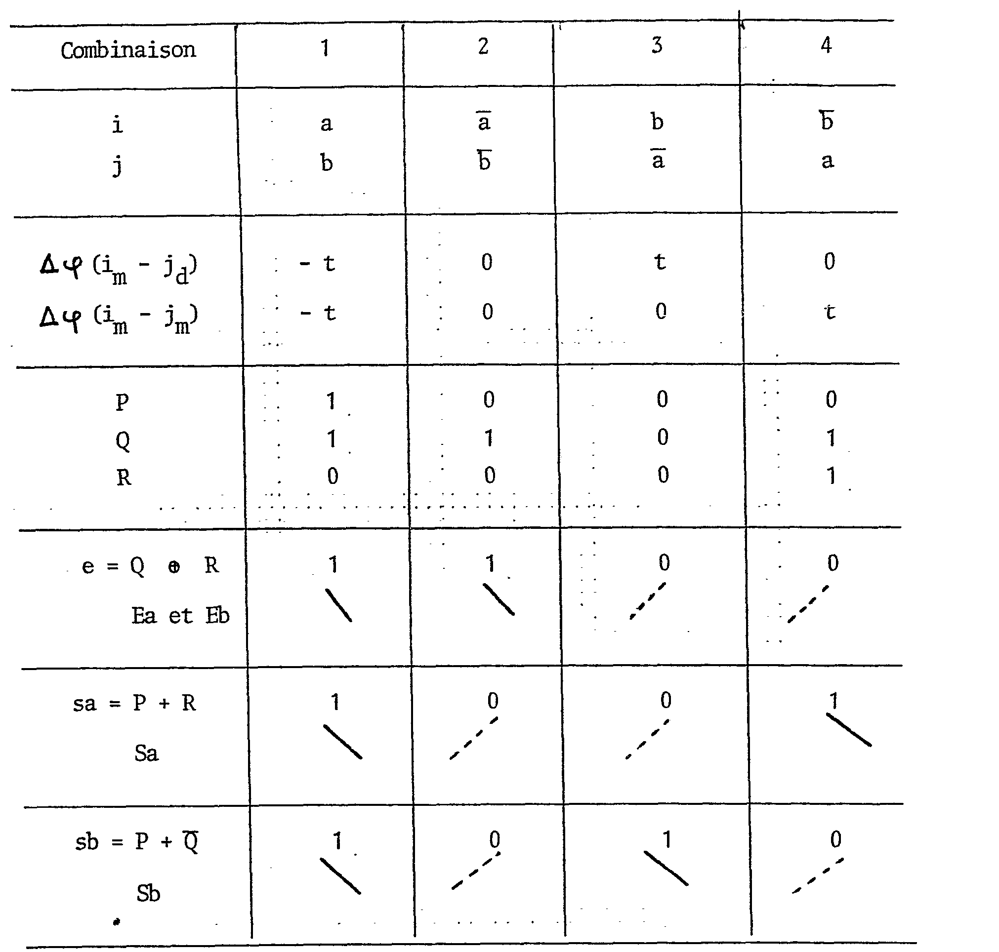
Dans ce tableau, on a indiqué un exemple de solution pour déduire le signal de commande e des commutateurs Ea, Eb, d'une part, et les signaux de commande sa , sb des commutateurs de sortie Sa, Sb d'autre part. Dans ce cas l'unité logique 78 comprend une porte OU-Exclusif 781 entre les entrées Q et R et la sortie e pour réaliser la fonction e = Q e R, une porte OU 782 entre les entrées P et R et la sortie sa pour réaliser la fonction sa = P + R et une seconde porte OU 783 pour réaliser la fonction sb = P + Q dont les entrées sont reliées directement à l'entrée P et, à travers un inverseur 784, à l'entrée Q et dont la sortie est sb.In this table, an example solution has been indicated for deducing the control signal e from the switches Ea, Eb, on the one hand, and the control signals sa, sb from the output switches Sa, Sb on the other hand. In this case the
On notera que, notamment, les conventions de signe et la réalisation décrites ci-dessus relatives au circuit de marquage 6 (Fig. 4) et au circuit de levée d'ambiguïté de phase 7 (Fig. 5) ne sont pas limitatives et que d'autres réalisations facilement concevables par l'homme du métier rentrent dans le cadre des revendications annexées, sans que cela modifie le résultat cherché, à savoir obtenir les signaux numériques initiaux A et B en entrée du régénérateur 40 quelle que soit l'ambiguïté de phase due à la démodulation.It will be noted that, in particular, the sign conventions and the embodiment described above relating to the marking circuit 6 (FIG. 4) and to the phase ambiguity removal circuit 7 (FIG. 5) are not limiting and that other embodiments easily conceivable by a person skilled in the art fall within the scope of the appended claims, without this modifying the desired result, namely obtaining the initial digital signals A and B at the input of the regenerator 40 whatever the ambiguity of phase due to demodulation.
Bien que le dispositif soit plus complexe, le procédé selon l'invention peut être appliqué à une modulation à 2N phases équirépar- ties. Par exemple pour la modulation à huit états de phase, les fronts montants ou descendants de l'un des trois signaux numériques issus du démultiplexage en triplet du signal numérique informatif sont marqués dans la partie émission. Dans ce cas, le circuit de levée d'ambiguïté de phase de la partie réception comprend sept circuits de détection de fronts et six différenciateurs de phase ainsi que des moyens de comparaison et de discrimination de phase et des moyens logiques de commande appropriés pour commander trois paires de commutateurs qui sont inclus dans le circuit d'aiguillage.Although the device is more complex, the method according to the invention can be applied to a 2 N equal-phase modulation. For example for the modulation with eight phase states, the rising or falling edges of one of the three digital signals resulting from the triplet demultiplexing of the informative digital signal are marked in the transmission part. In this case, the phase ambiguity removal circuit of the reception part comprises seven edge detection circuits and six phase differentiators as well as means for phase comparison and discrimination and logic control means suitable for controlling three pairs of switches that are included in the switch circuit.
Claims (12)
Applications Claiming Priority (2)
| Application Number | Priority Date | Filing Date | Title |
|---|---|---|---|
| FR8015505A FR2486741B1 (en) | 1980-07-11 | 1980-07-11 | METHOD AND DEVICE FOR LIFTING PHASE AMIGIGUE IN A QUADRIVALENT PHASE MODULATED LINK |
| FR8015505 | 1980-07-11 |
Publications (2)
| Publication Number | Publication Date |
|---|---|
| EP0044230A1 true EP0044230A1 (en) | 1982-01-20 |
| EP0044230B1 EP0044230B1 (en) | 1984-03-21 |
Family
ID=9244126
Family Applications (1)
| Application Number | Title | Priority Date | Filing Date |
|---|---|---|---|
| EP19810400937 Expired EP0044230B1 (en) | 1980-07-11 | 1981-06-12 | Method and arrangement for phase ambiguity resolution in a quadriphase modulation link |
Country Status (3)
| Country | Link |
|---|---|
| EP (1) | EP0044230B1 (en) |
| DE (1) | DE3162781D1 (en) |
| FR (1) | FR2486741B1 (en) |
Cited By (3)
| Publication number | Priority date | Publication date | Assignee | Title |
|---|---|---|---|---|
| GB2148669A (en) * | 1983-10-21 | 1985-05-30 | Philips Electronic Associated | Data receiver |
| US4528526A (en) * | 1983-05-31 | 1985-07-09 | Motorola, Inc. | PSK modulator with noncollapsable output for use with a PLL power amplifier |
| FR2559006A1 (en) * | 1984-01-31 | 1985-08-02 | Thomson Csf | CODING-DECODING DEVICE OF A BINARY DIGITAL SIGNAL TRAIN FOR FOUR-PHASE "OQPSK" DIGITAL MODULATOR-DEMODULATOR |
Citations (4)
| Publication number | Priority date | Publication date | Assignee | Title |
|---|---|---|---|---|
| US3736507A (en) * | 1971-08-19 | 1973-05-29 | Communications Satellite Co | Phase ambiguity resolution for four phase psk communications systems |
| US3809817A (en) * | 1972-02-14 | 1974-05-07 | Avantek | Asynchronous quadriphase communications system and method |
| US3855533A (en) * | 1972-06-28 | 1974-12-17 | Philips Corp | System including a transmitter and a receiver for the transmission of binary signals located in periodical clock intervals |
| US3931472A (en) * | 1972-02-14 | 1976-01-06 | Avantek, Inc. | Asynchronous quadriphase communications system and method |
-
1980
- 1980-07-11 FR FR8015505A patent/FR2486741B1/en not_active Expired
-
1981
- 1981-06-12 EP EP19810400937 patent/EP0044230B1/en not_active Expired
- 1981-06-12 DE DE8181400937T patent/DE3162781D1/en not_active Expired
Patent Citations (4)
| Publication number | Priority date | Publication date | Assignee | Title |
|---|---|---|---|---|
| US3736507A (en) * | 1971-08-19 | 1973-05-29 | Communications Satellite Co | Phase ambiguity resolution for four phase psk communications systems |
| US3809817A (en) * | 1972-02-14 | 1974-05-07 | Avantek | Asynchronous quadriphase communications system and method |
| US3931472A (en) * | 1972-02-14 | 1976-01-06 | Avantek, Inc. | Asynchronous quadriphase communications system and method |
| US3855533A (en) * | 1972-06-28 | 1974-12-17 | Philips Corp | System including a transmitter and a receiver for the transmission of binary signals located in periodical clock intervals |
Cited By (3)
| Publication number | Priority date | Publication date | Assignee | Title |
|---|---|---|---|---|
| US4528526A (en) * | 1983-05-31 | 1985-07-09 | Motorola, Inc. | PSK modulator with noncollapsable output for use with a PLL power amplifier |
| GB2148669A (en) * | 1983-10-21 | 1985-05-30 | Philips Electronic Associated | Data receiver |
| FR2559006A1 (en) * | 1984-01-31 | 1985-08-02 | Thomson Csf | CODING-DECODING DEVICE OF A BINARY DIGITAL SIGNAL TRAIN FOR FOUR-PHASE "OQPSK" DIGITAL MODULATOR-DEMODULATOR |
Also Published As
| Publication number | Publication date |
|---|---|
| EP0044230B1 (en) | 1984-03-21 |
| FR2486741A1 (en) | 1982-01-15 |
| FR2486741B1 (en) | 1988-03-11 |
| DE3162781D1 (en) | 1984-04-26 |
Similar Documents
| Publication | Publication Date | Title |
|---|---|---|
| FR2464603A1 (en) | RADIO COMMUNICATION RECEIVER IN FREQUENCY DISPLACEMENT MODULATION | |
| EP0054829B1 (en) | Method and apparatus for detecting the training sequence of an autoadaptive equalizer | |
| EP0419337B1 (en) | Digital signal encoding method, encoder and decoder for carrying out the method, regeneration method and regenerator therefore | |
| EP0559883A1 (en) | Process for digital transmission and direct conversion receiver. | |
| EP1677422A1 (en) | Apparatus for conversion of a transmitted signal into a binary signal | |
| FR2462826A1 (en) | MULTIPLE-PHASE MULTI-LEVEL MODULATION DIGITAL TELECOMMUNICATIONS SYSTEM | |
| EP0433198B1 (en) | Amplitude modulation transmission system with suppressed carrier maintaining the polarity of the transmitted signal | |
| EP0090728B1 (en) | Process for transmitting a hdbn coded signal with an auxiliary binary signal, coder and decoder according to the process and remote repeater supervision of a digital link by such an auxiliary signal | |
| EP0352159B1 (en) | Frequency drift tolerant method and device for demodulating constant envelope and continuous phase signals angularly modulated by a series of binary symbols | |
| CA1119677A (en) | Rhytm recovery device | |
| EP0044230B1 (en) | Method and arrangement for phase ambiguity resolution in a quadriphase modulation link | |
| EP0228528B1 (en) | Apparatus for implementing a code with a small digital sum variation in a fast digital transmission, and coding method using such an apparatus | |
| FR2465375A1 (en) | METHOD FOR THE SIMULTANEOUS TRANSMISSION OF SEVERAL DATA STREAMS ON A CHANNEL | |
| CA1092241A (en) | Encoding by transition of binary data | |
| FR2505111A1 (en) | CARRIER RECOVERY DEVICE FOR 16-STATE AMPLITUDE AND PHASE MODULATION AND DIGITAL DATA RECEIVING SYSTEM COMPRISING SUCH A DEVICE | |
| EP0032325A1 (en) | Binary phase shift modulations, and modulators | |
| FR2585908A1 (en) | METHOD AND RECEIVER FOR PACKET TRANSMISSION OF DIGITAL SIGNALS ON HIGH CAPACITY PATHWAY, IN PARTICULAR ON SATELLITE BROADCAST PATH | |
| EP0702468B1 (en) | Apparatus for the identification of a synchronisation sequence | |
| EP0396461A1 (en) | Device for synchronising a pseudo-binary signal with a phase-hopped regenerated clock signal | |
| FR2544571A1 (en) | CARRIER AND RHYTHM FREQUENCY RECOVERY FOR DIGITAL AND COMPUTERIZED PHASE AND AMPLITUDE MODULATION DIGITAL TRANSMISSION SYSTEMS AND COHERENT DEMODULATION | |
| EP0731588B1 (en) | Multiresolution phase modulation, for multicarrier systems | |
| EP0009557B1 (en) | Method and circuit for the simultaneous coding of two binary signal sequences into one pulse sequence, method and circuit for decoding the latter sequence, and their application to an interface transmitter-receiver | |
| CA1287126C (en) | Method and device for detecting false lockings of the reference signal onthe signal to be demodulated during a coherent digital demodulation | |
| FR2938988A1 (en) | METHOD FOR CONTINUOUS PHASE MULTISTATE MODULATION AND TRANSMITTER USING THE METHOD. | |
| EP0272956B1 (en) | Digital transmission system with a coherent demodulation adapted to the simultaneous transmission of two binary signals |
Legal Events
| Date | Code | Title | Description |
|---|---|---|---|
| PUAI | Public reference made under article 153(3) epc to a published international application that has entered the european phase |
Free format text: ORIGINAL CODE: 0009012 |
|
| AK | Designated contracting states |
Designated state(s): DE GB IT |
|
| 17P | Request for examination filed |
Effective date: 19820507 |
|
| ITF | It: translation for a ep patent filed |
Owner name: ING. PIOVESANA PAOLO |
|
| GRAA | (expected) grant |
Free format text: ORIGINAL CODE: 0009210 |
|
| AK | Designated contracting states |
Designated state(s): DE GB IT |
|
| REF | Corresponds to: |
Ref document number: 3162781 Country of ref document: DE Date of ref document: 19840426 |
|
| PGFP | Annual fee paid to national office [announced via postgrant information from national office to epo] |
Ref country code: DE Payment date: 19840627 Year of fee payment: 4 |
|
| PLBE | No opposition filed within time limit |
Free format text: ORIGINAL CODE: 0009261 |
|
| STAA | Information on the status of an ep patent application or granted ep patent |
Free format text: STATUS: NO OPPOSITION FILED WITHIN TIME LIMIT |
|
| 26N | No opposition filed | ||
| PG25 | Lapsed in a contracting state [announced via postgrant information from national office to epo] |
Ref country code: GB Effective date: 19890612 |
|
| GBPC | Gb: european patent ceased through non-payment of renewal fee | ||
| PG25 | Lapsed in a contracting state [announced via postgrant information from national office to epo] |
Ref country code: DE Effective date: 19900301 |