EP0052370A2 - A virtual storage data processing system - Google Patents
A virtual storage data processing system Download PDFInfo
- Publication number
- EP0052370A2 EP0052370A2 EP81109719A EP81109719A EP0052370A2 EP 0052370 A2 EP0052370 A2 EP 0052370A2 EP 81109719 A EP81109719 A EP 81109719A EP 81109719 A EP81109719 A EP 81109719A EP 0052370 A2 EP0052370 A2 EP 0052370A2
- Authority
- EP
- European Patent Office
- Prior art keywords
- memory
- address
- cache
- main memory
- data
- Prior art date
- Legal status (The legal status is an assumption and is not a legal conclusion. Google has not performed a legal analysis and makes no representation as to the accuracy of the status listed.)
- Granted
Links
Images


Classifications
-
- G—PHYSICS
- G06—COMPUTING; CALCULATING OR COUNTING
- G06F—ELECTRIC DIGITAL DATA PROCESSING
- G06F12/00—Accessing, addressing or allocating within memory systems or architectures
- G06F12/02—Addressing or allocation; Relocation
- G06F12/08—Addressing or allocation; Relocation in hierarchically structured memory systems, e.g. virtual memory systems
- G06F12/10—Address translation
- G06F12/1081—Address translation for peripheral access to main memory, e.g. direct memory access [DMA]
-
- G—PHYSICS
- G06—COMPUTING; CALCULATING OR COUNTING
- G06F—ELECTRIC DIGITAL DATA PROCESSING
- G06F12/00—Accessing, addressing or allocating within memory systems or architectures
- G06F12/02—Addressing or allocation; Relocation
- G06F12/08—Addressing or allocation; Relocation in hierarchically structured memory systems, e.g. virtual memory systems
- G06F12/0802—Addressing of a memory level in which the access to the desired data or data block requires associative addressing means, e.g. caches
- G06F12/0806—Multiuser, multiprocessor or multiprocessing cache systems
- G06F12/0815—Cache consistency protocols
- G06F12/0831—Cache consistency protocols using a bus scheme, e.g. with bus monitoring or watching means
- G06F12/0833—Cache consistency protocols using a bus scheme, e.g. with bus monitoring or watching means in combination with broadcast means (e.g. for invalidation or updating)
-
- G—PHYSICS
- G06—COMPUTING; CALCULATING OR COUNTING
- G06F—ELECTRIC DIGITAL DATA PROCESSING
- G06F12/00—Accessing, addressing or allocating within memory systems or architectures
- G06F12/02—Addressing or allocation; Relocation
- G06F12/08—Addressing or allocation; Relocation in hierarchically structured memory systems, e.g. virtual memory systems
- G06F12/10—Address translation
- G06F12/1027—Address translation using associative or pseudo-associative address translation means, e.g. translation look-aside buffer [TLB]
- G06F12/1045—Address translation using associative or pseudo-associative address translation means, e.g. translation look-aside buffer [TLB] associated with a data cache
Definitions
- the present invention relates to a virtual memory data processing system having an address translation unit shared by a plurality of processors in a memory control' unit connected to a main memory. More particularly, at least one of the plurality of processors is a job processor which accesses the memory with a virtual address to execute instructions and which has at least one cache memory which is accessed with the virtual address. At least one of the plurality of processors is a processor herein called a file processor which accesses the memory with the virtual address to read from and write in an external memory which is also called an auxiliary memory.
- a data processing system in which a main memory.is shared by a plurality of processors is generally called a multiprocessor system.
- the virtual memory system has been known well (for example, by U.S. Patent 3,829,840 issued on August 13, 1974).
- a main memory and an external memory are regarded to be apparently integral, and when information requested by a processor is not in the main memory but in the external memory, the system automatically transfers a portion of information in the main memory which is less frequently used to the external memory and tansfers the requested information from the external memory to the main memory.
- the transfer of information. from the main memory to the external memory is called a roll-out and the transfer of information from the external memory to the main memory is called a roll-in.
- the main memory and the external memory are usually divided into units called pages, respectively.
- An address for the memory access by the processor is given by a virtual address, a high order address field of which is used to look up the translation table to effect the translation to the physical address.
- the translation table in many cases, comprises a segment table and a page table to effect two-level address translation.
- the translation tables require a large memory capacity as described above, they are usually put on the main memory. If the translation tables on the main memory are checked each time the processor requests the memory access, three or more memory accesses take place for each memory access request and an overhead is not negligible.
- TLB translation lookaside buffers
- the processor requests the memory access, the presence or absence of the corresponding address in the TLB is first checked, and if it is present the memory access to the translation table for the address translation is not necessary and the memory access is effected with less overhead for the address translation.
- the address translation units with the TLB's are provided one for each of the processors and the virtual memory system is attained with the aid of the control units in the processors.
- each of the processors is usually provided with a high speed memory called a cache memory.
- the cache memory stores a copy of a portion of content of the main memory and it usually has a speed which is 5 - 10 times as fast as the speed of the main memory.
- the cache memory is first examined if it stores the requested data or not, and if it does, the data is sent to the processor and if it does not, the main memory is accessed.
- the TLB, the cache memory and the main memory are connected to the processor in this order as viewed from the processor. This is based on the consideration that the cache memory is a copy of a portion of the main memoyr. Thus, the cache memory has to be accessed after the virtual address has been translated to the physical address.
- the cache memory is accessed after the virtual address from the processor has been translated to the physical address by the TLB.
- the entries to the translation table and to the TLB are updated and it is reported to that processor as well as other processors to clear the corresponding portions.
- TLB purge This is one of important points in constructing the multiprocessor system.
- a conventional job processor uses the virtual address to access the memory but an I/O processor accesses the memory with the physical address because it has no TLB. As a result, when the address is exchanged between those processors the overhead increases.
- a unit for accessing an instruction is separate from a unit for accessing an operand and they have cache memories of their own to attain a high speed operation.
- each unit must have the TLB and hence the hardware increases.
- Japanese Patent Application Laid-open No. 38649/1981 laid-open on April 13, 1981 also discloses a technique to access the cache memory with the virtual address, but it does not discuss the solution to the above problems.
- Japanese Patent Application Laid-open No. 65439/1979 laid-open May 26, 1979 discloses a system to share an address translation unit with a plurality of processors.
- a multiprocessor system can be economically constructed.
- it does not show the cache memory and does not point out the problems nor does it suggest the solution thereto.
- the present invention is applicable to a configuration having a plurality of processors at least one of which has a cache memory accessed with a virtual address, and an address translation unit shared by all of the processors.
- the address translation unit is shared by the plurality of processors, when a real address corresponding to a requested virtual address is not in the main meory, that is, when a page fault occurs, the corresponding page has to be transferred to the main memory from an external memory.
- This transfer is controlled by a file processor. During the transfer, that is, during the paging, the paging area must be prevented from being accessed by the processors other than the file processor.
- the address translation unit is shared by the plurality of processors, the address translation unit is a neck to throughput as the number of processors increases.
- an object of the present invention to provide a data processing system having reduced amount of hardware of the address translation unit and reduced effective memory access time to resolve the problems of the cache memory.
- the cache memory used in the present invention includes invalidating means which receives a virtual address when the file processor writes to the main memory and, when a data block corresponding to the virtual address is retained in the cache memory, inhibits the use of that data block.
- the address translation unit used in the present invention discriminates the access by the file processor and the accesses by other processors.
- the memory controller used in the present invention comprises a first register for latching the virtual address sent from the processor and a second register for retaining the translated physical address to be used as the address when the main memory is accessed, and sequentially and parallelly carries out the loading of the virtual address sent from the processor to the first register, the address translation of the content of the first register and the loading of the translated address to the second register, and the accessing of the main memory by the contett of the second register.
- the second problem is an essential problem encountered when the cache is accessed with the virtual address. This will be discussed in further detail.
- the address translation table is updated when (i) paging fault occurs during the execution of a program and a requested page is rolled in or a.page is rolled out to prepare a vacant area, and (ii) a program generated is allotted to a virtual address or a program is deleted. In such cases, data rolled out of the main memory remains in the cache memory or a previous programs remains in the cache memory after a new program has been generated. With respect to the fact that the rolled-out information remains in the cache, if the cache memory is considered as a cache in a space including the external memory: no problem will be encountered by reading out the rolled-out information.
- the cache and the main memory are both updated for each write access to the main memory. Accordingly, every address passes through the address translation unit which checks if the corresponding page is on the main memory or not. Accordingly, in a program executed using the rolled-out page, the program continues to run so far as cache hit occurs, and when cache miss or write request to the main memory occurs, page fault takes place.
- the requested page is (a) on the main memory, (b) being paged, or (c) not on the main memory.
- Ordinary processor can access the main memory only in the condition (a) and the file processor which transfers data to and from the external memory can access even in the condition (b).
- the address translation unit checks if the above rule is met.
- the corresponding block in the cache memory is invalidated and no cache hit occurs thereafter. If the page fault takes place in the read access; the corresponding block is prevented from being written to the cache.
- a currently executed program When a currently executed program is terminated and a new program is generated at the same virtual address, it is usually transferred from the external memory.
- means for invalidating the cache during the transfer from the external memory may be provided. More particularly, the transfer from the external memory to the main memory is effected by the virtual address and the cache memory monitors the address, and if the corresponding block is present in the cache memory it is invalidated.
- the third problem is the storage protection.
- the virtual address can allocate a unique storage protection key to each program better than the physical address.
- the write protection key must be checked because the write address always passes through the address translation unit.
- the corresponding block in the cache memory is invalidated to prevent the data written in the cache memory from being used. Consideration will become necessary with respect to the execution, protection because if a requested data for memory read is in the cache the read request is sent back and not supplied to the address translation unit.
- the cache memory is divided into the insutruction cache and the data cache and the read request is not supplied to the cache memory if an execution protection error is detected.
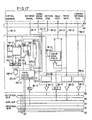
- numeral 10 dentoes a main memory for storing programs and data, and it is connected to a common bus 50 through a memory bus 11 and a memory control unit (MCU) 13.
- MCU memory control unit
- Numeral 20 dentoes an external memory which stores programs and data to be transferred to the main memory 10, and it is connected to the common bus 50 through an external memory bus 21 and a file control processor (FCP) 22.
- Numeral 30 denotes an I/O processor CIOP)' which controls data transfer between various I/O devices not shown.
- Numeral 40 denotes a job processor (_JOBP), only one being shown in Fig. 1. It executes a program (instructions).
- the job processor 40 comprises an instruction cache 41, a data cache 42, an instruction (I) unit 43 and an execution (E) unit 44.
- the instruction cache 41 and the I unit are interconnected through a bus 45
- the data cache 42 and the E unit 44 are interconnected through a bus 46.
- the I unit 43 and the E unit 44 are interconnected through a bus 47.
- the file processor 22, the I/O processor 30 and the job processor 40 are connected to the common bus 50 and can access the main memory 10 through the memory control unit 12.
- the job processor 40 processes data in a pipelined fashion with the I unit 43 and the E unit 44 and has the instruction cache 41 and the data cache 42 for the respective units.
- the data handled by the program are also called operands and the data cache is also called an operand cache.
- the I unit 43 fetches an instruction word to be executed, the presence or absence of the instruction word on the instruction cache 41 is checked, and if it is present the data is transferred to the I unit 43 as the instruction word through the bus 45. If it is absent, a virtual address of the instruction word is transferred to the memory control unit 12 through the common bus 50.
- the memory control unit 12 translates the virtual address to the physical address to access the main memory 10 through the memory bus 11.
- the accessed data (instruction) is sent to the instruction cahce 41 through the common bus 50 and to the I unit 43 through the bus 45, and processed in the I unit 43 and stored in the instruction cache 41.
- the I unit 43 decodes the fetched instruction to instruct "what is to be done” to the E unit 44. Based on the instructions, the E unit 44 collects necessary data from internal registers and the data cache 42 (or from the main memory 10 if the data is not on the data cache 42), processes the data and loads the result in the internal register or the main memory 10. When the result is to be stored in the main memory 10, if the data at the corresponding location has been stored in the data cache 42, that data is updated.
- the common bus 50 comprises an initiation bus 55, a data bus 56 and a response bus 57 which are used to actually transfer information: and an initiation bus request line 51, a data bus request line 52, a response bus request line 53 and an interlock signal line 54 which are used to allocate the buses 55 to 57 to the processors and the memory control unit.
- Those buses and lines are used in a time division fashion.
- the buses 55 to 57 carry the following information.
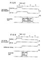
- Fig. 3 illustrates a manner in which the buses 55 to 57 are used. As shown in Fig. 3, three combinations;
- JOBP issues a memory read initiation signal to MCU and corresponding read data is sent back in time slots N and N.+ 1.
- IOP issues a memory write initiation signal to MCU and corresponding data is sent back in a time slot N + 2.
- the initiation signals and the responses are transferred in a split transfer fashion over the common bus 50.
- the main memory 10 is designed to allow multiple memory accesses.
- the occupation control must be done. This is effected by issuing requests 51 to 53 from the processors and the memory control unit which desire the transfer to the desired buses one time slot before the transfer and granting the transfers with a priority order.
- the priority order may be given in various ways although detail thereof is not explained here.
- the response bus request has a higher priority than the initiation bus request because if the send-back of the response is prevented by the initiation bus request, the initiation process in the memory control unit is interrupted resulting in a deadlock condition. In the present embodiment, if the request for the data read response b in Fig. 3 and the request for the data write initiation c compete, the former is given a higher priority,
- Fig. 5 shows a manner of the occupation control.
- the JOBP 40 and the IOP 30 issue the initiation bus requests 51 in order to initiate the read operation.
- the JOBP 40 uses the initiation bus 55 in the time slot 1 to initiate the read operation and withdraws. the occupation request.
- the IOP 30 continues to issue the initiation bus request 51 in the time slot 1. After the occupation request by the JOBP 40 has been withdrawn in the time slot 1, the IOP 30 is allowed to initiate the read operation in the time slot 2.
- the initiation bus request 51 is accepted as shown in Fig. 6 and the processor issues the interlock signal 54 indicating the occupation of the initiation bus 55, in the time slot in which information is transferred out to the initiation bus 55.
- This interlock signal prevents the initiation bus requests 51 from other processors from being accepted. This may be done by a circuit shown in Fig. 7.
- Each processor has a separate priority circuit 6 1 for the occupation requests 51 to 53.
- the interlock signal line 54 is an open collector line.
- the interlock signal 54 When the interlock signal 54 is not present, the occupation requests 51 to 53 are examined by the priority circuit 61, and if the initiation bus request 51 has the highest priority, an accept signal 64 for the occupation of the initiation bus 55 is issued through an AND gate 62 and an OR gate 63. Accordingly, the processor is allowed to transfer out information to the initiation bus in the next time slot. If an interlock request signal 65 is being issued from the processor at this time, a J-K flip-flop 66 is set through an AND gate 68 and an interlock signal 54 is produced. The interlock signal 54 lasts until an interlock release signal 67 is issued and the processor continuously occupies the initiation bus 55 during this period. When the interlock signal is issued from other processor, the output of the priority circuit 61 is inhibited by the AND gate 62 so that the initiation bus request accept signal 64 is not produced. As a result, the processor cannot use initiation bus 55 and cannot initiate the memory.
- the MCU 12 carries out ordinary memory access processing as well as the address translation from the virtual address to the physical address and the protection check.
- the read process and the write process are staged in stages 1- 05 and 1' - 5', as shown in Figs. 8A and 8 B , so that a plurality of accesses can be processed in an overlapped or parallel fashion as shown in Fig. 8C.
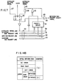
- Fig. 9 shows an exemplary configuration of the MCU 12.
- the process stages shown in Figs. 8A and 8B carry out the following operations.
- VA virtual address
- FUN type of access
- RAKEY access key
- the address translation unit 75 checks if the page specified by the virtual address (VA) is in the main memory 10 or not, and if it is, the address translation unit 75 translates it to the physical address. If it is not in the main memory 10, the page fault takes place.
- VA virtual address
- a protection check circuit 76 checks if the access is permitted or not.
- the address translation unit 75 and the protection check circuit 76 will be explained in detail hereinlater.
- the protection check result and the page fault information as well as other error information are loaded to an access register 72 as a return code (RC) together with the type of access (FUNC) and the physical address (PA).
- RC return code
- FUNC type of access
- PA physical address
- the memory control unit 77 issues a memory initiation 151 to the main memory 10 at the physical address (PA) on the access register 72, and after the main memory 10 has received the memory initiation, the memory control unit 72 transfers the type of access (FUNC) and the return code (RC) to a temporary store register 73.
- PA physical address
- the memory control unit 72 transfers the type of access (FUNC) and the return code (RC) to a temporary store register 73.
- the memory initiation is not issued and the information is transfarred to the temporary store register 73.
- the read data 154 is received from the main memory 10 through the memory bus 11, and the type of access (FUNC) and the return code (RC) are trnsferred to a common bus send-out register 74.
- FUNC type of access
- RC return code
- the read data 154 is transferred to the data bus 56 through a bus 155, and an end signal and the return code (RC) are transferred to the response bus 57 through a bus 156 to send them back to the requesting processor.
- RC return code
- VA virtual address
- FUNC type of access
- AWY access key
- WD write data
- the type of access (FUNC) and the return code (RC) are trnasferred to the common bus send-out register 74.
- the response bus request 53 is trnasferred to the common bus 50.
- the end signal and the return code (RC) are transferred to the response bus 57 through the bus 156 to send them back to the requesting processor.
- Fig. 8C the read and write processes are staged and the stages of different numbers for the different accesses can be processed in parallel as shown in Fig. 8C, in which (a) 4-byte read initiation, (b) 4-byte write initiation and (c) 16-byte read initiation are received from the common bus 50 at the time slots 0, 1 and 2, respectively. Looking at the time slot 2, the memory read initiation 3 for (a), the address translation and protection check 2' for (b) and the receipt of the read initiation from the common bus 1 for (c) are carried out in parallel. The 16-byte read (c) repeats the stages (a) to 5 four times because of 4-byte memory interleaving. This will be further explained below.
- Fig. 10A and 10B show a configuration of the main memory 10.
- Memory boards (MB) 14 (14a - 14d) have 4-byte data width and the memory boards 14a, 14b, 14c and 14d have data addresses given in four-byte unit with lower two bits thereof being 00, 01, 10 and 11, respectively.
- a 16-byte data is divided into 4-byte groups which are stored in the memory boards 14a, 14b, 14c and 14d, respectively. Accordingly, in the 16-byte read operation, the memory boards can be initiated sequentially as shown in Fig. 8C to read out the data without competition among the memory boards 14.
- the 16-byte read is mainly used in a block transfer to transfer data to the cache memory when the cache miss occurs.
- the I unit 43 or the E unit 44 accesses the instruction cache 41 or the data cache 42, it accesses in a smaller unit (4-byte unit in the illustrated example) than 16-byte unit. Accordingly, in the 16-byte read, the access is controlled such that the I unit 43 or the E unit 44 receives the requested 4-byte data earlier than remaining data in order to reduce the access time. To this end, the sequence of initiation of the memory boards 14 by the MCU 12 are changed.
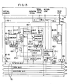
- Fig. 11 shows the address translation unit 75 of Fig. 9 and supporting circuits in detail and Fig. 12 shows flow of address translation operation.
- a translation table 130 from the virtual address to the physical address is located in the main memory 10 because of its large memory capacity. Since the virtual address is translated to the physical address at each memory access, the overhead increases if the main memory 10 is accessed. Accordingly, a TLB 110 for storing the translation information of lately accessed addresses is provided in the MCU 12.
- the TLB 110 stores the contents of the lately used pages of the address translation table 130 so that high speed address translation is attained.
- the content of each of the pages in the TLB 110 includes a valid bit (V) lll, a connect bit (C) 112, a portion of the virtual address (VPA) 113, a portion of the-physical address (PPA) 114, an execution protection bit (EP) 115 and a storage key (SKEY) 116.
- the bit V 111 and the bit C 112 indicate the current status of the page. When the bit V 111 is "0", it indicates that the content of the page in the TLB 110 is not valid (invalid).
- both the bit V 111 and the bit C 112 are "1" they indicate that the page is being transferred between the main memory 10 and the external memory 20, that is, paging condition.
- bit V 111 is "1” and the bit C 112 is "0" they indicate that the page is in the main memory 10 and the memory access is permitted.
- the paging condition is indicated in order to prevent the paging area from being accessed except the paging access from the FCP 22.
- the access to the area being paged by the FCP 22 passes through the common address translation unit 75. If the access to the paging area by other processor is permitted, data may be broken or lost. Accordingly, as described above, when both the bit V 111 and the bit C 112 are "1", only the paging access by the FCP 22 is permitted to avoid the difficulty explained above.
- the portion of the virtual address (VPA) 113 is used to check if the translation pair for the corresponding virtual address (VA) has been registered in the TLB 110 when the address is to be translated by the TLB 110, and the portion of the physical address (PPA) 114 is used to prepare the physical address (PA) when the translation pair is in the TLB 110.
- the virtual address (VA) includes a segment address (SA) 121, a page address (PA) 122 and a displacement (DISP) 123.
- SA segment address
- PA page address
- DISP displacement
- the portion of the physical address (PPA) 114 is combined with the displacement (DISP) 123 to prepare the physical address (PA).
- the execution protection bit (EP) 115 prevents wrong instruction fetch or execution for data.
- the execution protect error is detected by the protection check circuit 76 if instruction is fetched from an area for which the execution protection bit is "1". Where the JOBP 40 has the insturction cache 41 and the data cache 42 separately as is the case of the present embodiment, the access to that area from the instruction cache 41 causes the execution protect error.
- the storage key (SKEY) 116 is used for the write protection.
- the protection check circuit 76 checks the storage key (SKEY) 116 and the access key (AKEY) transferred from the requesting processor to determine if the write access is permitted or inhibited, and if it is inhibited the write protection error takes place.
- the access key (AKEY) is compared with the storage key (SKEY) 116 to check the write protection error as described above. It also includes information on the paging address from the FCP 22 and the insturction fetch and is used for the protection check of such information.
- the memory access is classified into the following two major categories:
- the accesses (1) and (2) are discriminated by the access key (AKEY) which is supplied to the address translation controller 125 through the signal line 140.
- the virtual address from the processor (JOBP 40 or IOP 30) is loaded to a virtual address register 1 20 in the common bus receiving register 71 in the MCU 12 through the common bus 50.
- a portion 120-2 of the segment address (SA) 121 and the page address (PA) 122 is used to address the TLB 110.
- the bit V 111 and the bit C 112 of the entry in the TLB 110 addressed by the address 120-2 are supplied to the address translation controller 125.
- the subsequent process is one of the following three 1- 3 depending on a particular pattern. It corresponds to a step F05 in the flow of Fig. 12.
- Bit V 111 is “0” and bit C 112 is “0":
- TLB hit signal When the TLB hit signal is not present, it indicates TLB miss. Accordingly, like in the case of (D the translation table 130 on the main memory 10 is read out (F10).
- Bit Vlll is “1” and bit C 112 is “0”:
- the TLB hit signal 141 is first checked (F30), and if it is not present, the protection error signal 143 from the protection check circuit 76 is checked. If no error, the displacement 123 in the virtual address register 120 and the portion 114 of the physical address on the TLB 110 are combined to form the physical address on the access register 72 through a selector 128, and the physical address is transferred to the memory address bus 152, and a memory initiation signal 151 is produced from the memory control unit 77 to access the main memory 10 (F40).
- the virtual address from the FCP 22 is loaded to the virtual address register 120 in the MCU 12 through the common bus 50.
- TLB 110 is accessed first in this case, too.
- the subsequent process is one of the following three depending on a particular pattern of the bit V 111 and the bit C 112 of the accessed entry of the TLB 110.
- Bit V 111 is “0” and bit C 112 is “0":
- the translation table 130 on the main memory 10 is read out (F10).
- the TLB hit signal 141 is checked (F30). If the TLB hit is indicated, the main memory 10 is accessed with the physical address prepared in the access register 72 (F40).
- the translation table 130 on the main memory 10 is read out (F10).
- the TLB hit signal 141 is checked (F215). If the TLB hit signal 141 is present, it indicates that the inhibited area was accessed, and error condition is informed to the FCP 22 (F220).
- the table 130 comprises a page table 132 retaining information necessary for the address translation and a segment table 131 retaining leading addresses of the page table 132.
- the content of a register (STOR) 126 retaining the leading address of the segment table and the segment address (SA) in the virtual address register 120 are combined in an adder 127 to prepare a physical address by which the segment table 131 is addressed to read out the content of the addressed location to the read data bus 155.
- the data includes the leading address of the page table 132, and this leading address and the page address (PA) 122 in the virtual address register 120 are combined in the adder 127 to prepare an address to read out information necessary for the translation from the page table 132 (F10).
- the page table 132 contains bits M and information in the TLB 110 excluding the bit V 111 and the portion (VPA) 113 of the virtual address.
- the bit M and the bit C are supplied to the address translation controller 125 through a portion 155-1 of the read data bus 155. Depending on a particular pattern of those bits, one of the following processes is carried out.
- a missing page fault signal 142 is produced to inform the page fault to the processor (F45).
- Bit M is “0” and bit C is “1":
- the memory access is inhibited and the missing page fault signal 142 is produced (F45).
- the memory access by the FCP it is registered in the TLB 110 and the memory is accessed (F20).
- a portion 155-2 of the read data, the portion 120-1 of the virtual address and the bit V "1" are registered in the TLB 110 (F20), and the bits V and C are checked.
- the address translation unit 75 can translate the virtual address to the physical address in a concentrated way to the memory access by the virtual address from the processor and the control to the address translation is simplified.
- the processor interrupts the task which it has been executing and initiates the FCP 22 to load the page containing the requested address to the main memory 10.
- the FCP 22 responds to the initiation signal to read out the corresponding page and issues a termination interruption signal at the end of readout. Since the necessary page has been rolled in the main memory 10 by this time, the processor resumes the interrupted task. During the interruption of the task, the processor executes other tasks.
- Fig. 13 shows an exemplary configuration of the instruction cache 41.
- the data copied from the main memory 10 is on a cache data field 81-I, the addresses of that data are on a directory 82-I and. an invalidate directory 83-I, and information indicating validity of the addresses is on a valid bit register 84-I.
- the contents of the directory 82-I and the invalidate directory 83-I are identical and they are separated to enhance the performance.
- the former is used to check whether the data accessed by the I unit 43 is in the cache data field 81-I or not and the latter is used to check the invalidation process for invalidating old data when the data written in the main memory 10 by other processor is read in the cache data field 81-I.
- the instruction cache 41 does not carry out write access.
- Fig. 14 shows flow in the cache miss of the read access and Fig. 15 shows flow in the invalidation process.
- a retry is carried out for the hard error.
- the above signals are not sent back, but if the number of times of retry exceeds a predetermined number, that is, in the case of retry over, the above signals are sent back to report the error condition.
- the read data from the main memory 10 is then written into the cache data field 81-1.
- the instruction cache controller 162-1 issues a valid bit clear signal 171 to the valid bit register 84-I which was set in the stage 4 to clear the valid bit register 84-I to inhibit the use of the corresponding data in the cache data field 81-1. If the hard error occurred in the stage 5 and the retry over is not present (that is, when the condition (a) of Fig. 14B is met), the process jumps to the stage 2] to carry out the retry.
- the read access process has thus far been explained.
- the cache (both the instruction cache and the data cache) need the invalidation process as described above. This process is explained below.
- Fig. 16 shows a time chart for competing invalidation process of the cache when the read access results in the cache miss and the main memory 10 is accessed to read data and when the main memory 10 is write-accessed by other processor.
- the invalidation process is shown by hatched blocks.
- the invalidate directory 83-I is checked in the time slots 2 and 4 and the valid bit register 84-I is cleared in first halves of the time slots 3 and 5.
- the read access which resulted in the cache miss transfers the address to the initiation bus 55 in the time slot 2.
- the main memory 10 is accessed after the write access on the initiation bus 55 in the time slot 1 and before the write access on the initiation bus in the time slot 3. Accordingly, in order to maintain the coincidence-of the data in the cache and the main memory 10, the address of the read access which caused the cache miss must be written into the invalidate directory 83-I between the time slots 2 and 4 in which the write access checks the invalidate directory 83-I, and the valid bit register 84-I must be set between the time slots 3 and 5 in which the valid bit register 84-I is invalidated. Such control is needed because a plurality of memory accesses are simultaneously processed in the main memory 10.
- the directory 82-I and the invalidate directory 83-I since the address information is stored in two locations, the directory 82-I and the invalidate directory 83-I, only the invalidate directory 83-I is subject to the above restriction. Where the directory is at only one location, the directory is subject to the above restriction.
- Fig. 17 shows an exemplary configuration of the data cache 42.
- An invalidate circuit 180-D is omitted because it is identical to the cache 41.
- the like numerals with different suffixes to those shown in Fig. 13 denote like or corresponding elements.
- suffixes I are added while in the data cache of Fig. 17 suffixes D are added.
- a main difference from the instruction cache 41 resides in that the data cache must support the write access.
- a common bus sending buffer 89-D is provided and in the write operation the virtual address 92-D, the write data 95-D and the control information 96-D are stored in the buffer 89-D and the termination signal 93-D is sent back to the E unit 44 to make it ready for the next process.
- the address used for the write initiation to the main memory 10 from the data cache 42 is also loaded to the register 87-D (included in the invalidate circuit 180-D) of the data cache through the initiation bus 55. Since it was issued from the data cache, the data cache controller 162-D sends a signal 173 to the invalidate circuit 180-D to inhibit the invalidation process. Since the instruction cache 41 does not carry out the write access, no signal corresponding to the signal 173-D is issued.
- the present invention provides the data processing system having a plurality of processors at least one of which has a cache memory accessed with the virtual address, and an address translation unit which is shared by all of the processors.
Abstract
Description
- The present invention relates to a virtual memory data processing system having an address translation unit shared by a plurality of processors in a memory control' unit connected to a main memory. More particularly, at least one of the plurality of processors is a job processor which accesses the memory with a virtual address to execute instructions and which has at least one cache memory which is accessed with the virtual address. At least one of the plurality of processors is a processor herein called a file processor which accesses the memory with the virtual address to read from and write in an external memory which is also called an auxiliary memory.
- A data processing system in which a main memory.is shared by a plurality of processors is generally called a multiprocessor system.
- One of the problems to be resolved in the multiprocessing system is a virtual memory system. The virtual memory system has been known well (for example, by U.S. Patent 3,829,840 issued on August 13, 1974). In the virtual memory system, a main memory and an external memory are regarded to be apparently integral, and when information requested by a processor is not in the main memory but in the external memory, the system automatically transfers a portion of information in the main memory which is less frequently used to the external memory and tansfers the requested information from the external memory to the main memory.
- The transfer of information. from the main memory to the external memory is called a roll-out and the transfer of information from the external memory to the main memory is called a roll-in.
- In order to control the roll-in and the roll-out, the main memory and the external memory are usually divided into units called pages, respectively.
- Information indicating whether the respective pages are currently in the main memory and corresponding physical addresses (which are also called real addresses) on the main memory if the pages are in the main memory is stored in a translation table for each of the pages.
- An address for the memory access by the processor is given by a virtual address, a high order address field of which is used to look up the translation table to effect the translation to the physical address.
- Since as many such translation tables as the number of pages of the virtual addresses are required, a large memory capacity is necessary. Accordingly, in order to reduce the necessary memory capacity, the translation table, in many cases, comprises a segment table and a page table to effect two-level address translation.
- Since the translation tables require a large memory capacity as described above, they are usually put on the main memory. If the translation tables on the main memory are checked each time the processor requests the memory access, three or more memory accesses take place for each memory access request and an overhead is not negligible.
- Accordingly, many virtual memory processors include high speed buffers called translation lookaside buffers (TLB) which store the physical addresses corresponding to the recently used virtual addresses.
- In such a system,'if the processor requests the memory access, the presence or absence of the corresponding address in the TLB is first checked, and if it is present the memory access to the translation table for the address translation is not necessary and the memory access is effected with less overhead for the address translation. In the prior art system, the address translation units with the TLB's are provided one for each of the processors and the virtual memory system is attained with the aid of the control units in the processors.
- On the other hand, in order to enhance the performance, each of the processors is usually provided with a high speed memory called a cache memory. The cache memory stores a copy of a portion of content of the main memory and it usually has a speed which is 5 - 10 times as fast as the speed of the main memory.
- When the processor requests the memory access, the cache memory is first examined if it stores the requested data or not, and if it does, the data is sent to the processor and if it does not, the main memory is accessed.
- In the prior art virtual memory system having the cache memory, the TLB, the cache memory and the main memory are connected to the processor in this order as viewed from the processor. This is based on the consideration that the cache memory is a copy of a portion of the main memoyr. Thus, the cache memory has to be accessed after the virtual address has been translated to the physical address.
- Those prior art systems have the following difficulties.
- Firstly, an effective memory access time is long.
- This is because the access to the cache memory by the processor must pass through the TLB. In other words, the cache memory is accessed after the virtual address from the processor has been translated to the physical address by the TLB.
- Secondly, since the TLB is required by each of the processors, the hardware increases as the number of processors increases and the offsets of the TLB's must be compensated, which is a complicated job.
- In order to compensate the offsets of the TLB's, when one of the processors swaps a papge, the entries to the translation table and to the TLB are updated and it is reported to that processor as well as other processors to clear the corresponding portions.
- This is usually called a TLB purge which is one of important points in constructing the multiprocessor system.
- Thirdly, a conventional job processor uses the virtual address to access the memory but an I/O processor accesses the memory with the physical address because it has no TLB. As a result, when the address is exchanged between those processors the overhead increases.
- Forthly, in a highly pipline controlled processor, a unit for accessing an instruction is separate from a unit for accessing an operand and they have cache memories of their own to attain a high speed operation. In a prior art system of this type, each unit must have the TLB and hence the hardware increases.
- In order to resolve the above difficulties, it has been taught in the above-referenced U.S. Patent 3,829,840 to access the cache memory with the virtual address and translate the address onlyif it does not hit: In this system, it is not necessary to translate the address at every access to the cache memory and hence a high speed operation can be attained.
- However, it is pointed out in the U.S. Patent 3,829,840 that this system cannot be adopted because of the following disadvantages:
- (1) The system does not work satisfactorily when two different virtual addresses refer to the same physical address. This is because when a content of a virtual address is updated a content of the-cache memory specified by another virtual address indicating the same physical address must have been updated.
- (2) When a content of the page of segment table is updated, a scan is required to invalidate the cache memory.
- (3) Since storage protection keys are associated with the physical addresses, protection check is impossible.
- Japanese Patent Application Laid-open No. 38649/1981 laid-open on April 13, 1981 also discloses a technique to access the cache memory with the virtual address, but it does not discuss the solution to the above problems.
- Japanese Patent Application Laid-open No. 65439/1979 laid-open May 26, 1979 discloses a system to share an address translation unit with a plurality of processors. In this system, because of the share with the plurality of processors, a multiprocessor system can be economically constructed. However, it does not show the cache memory and does not point out the problems nor does it suggest the solution thereto.
- The present invention is applicable to a configuration having a plurality of processors at least one of which has a cache memory accessed with a virtual address, and an address translation unit shared by all of the processors.
- Most difficult problem in this system is, as pointed out in the U.S. Patent 3,829,840, that when a page or segment table of a main memory is updated it is not conveyed to the cache memory and hence the content of the cache memory does not exactly reflect the content of the main memory.
- In addition, since the address translation unit is shared by the plurality of processors, when a real address corresponding to a requested virtual address is not in the main meory, that is, when a page fault occurs, the corresponding page has to be transferred to the main memory from an external memory. This transfer is controlled by a file processor. During the transfer, that is, during the paging, the paging area must be prevented from being accessed by the processors other than the file processor.
- Furthermore, since the address translation unit is shared by the plurality of processors, the address translation unit is a neck to throughput as the number of processors increases.
- It is, therefore, an object of the present invention to provide a data processing system having reduced amount of hardware of the address translation unit and reduced effective memory access time to resolve the problems of the cache memory.
- It is another object of the present invention to provide a data processing system which allows the page processor to carry out the paging operation without difficulty when the page fault occurs.
- It is a further object of the present invention to provide a data processing system having a high speed memory controller including the address translation unit to prevent the reduction of throughput.
- The cache memory used in the present invention includes invalidating means which receives a virtual address when the file processor writes to the main memory and, when a data block corresponding to the virtual address is retained in the cache memory, inhibits the use of that data block.
- The address translation unit used in the present invention discriminates the access by the file processor and the accesses by other processors.
- The memory controller used in the present invention comprises a first register for latching the virtual address sent from the processor and a second register for retaining the translated physical address to be used as the address when the main memory is accessed, and sequentially and parallelly carries out the loading of the virtual address sent from the processor to the first register, the address translation of the content of the first register and the loading of the translated address to the second register, and the accessing of the main memory by the contett of the second register.
- The present invention is pointed out particularly in the appended claims. The above and other objects and advantages of the present invention will be better understood by referring to the following description taken in conjunction with the accompanying drawings, in which:
- Fig. 1 shows an overall configuration of a data processing system to which the present invention is applied;
- Fig. 2 shows a configuration of a common bus shown in Fig. 1;
- Fig. 3 shows a chart for illustrating particular portions of the common bus used for respective accesses;
- Fig. 4 illustrates the use of the common bus;
- Fig. 5 illustrates occupation control of the common bus;
- Fig. 6 illustrates occupation control of the common bus when an interlock signal is present:
- Fig. 7 shows a configuration of an occuprtion control circuit;
- Figs. 8A to 8C show process flow in an MCU and illustrate overlapped process of a plurality of access requests in the MCU;
- Fig. 9 shows a configuration of the MCU;
- Figs. 10A and 10B show a configuration of a memory board and illustrate a sequence of data send-back for 16-byte read;
- Fig. 11 shows an address translation unit having a TLB;
- Fig. 12 shows a flow for address translation;
- Fig. 13 shows a configuration of an instruction cache;
- Figs. 14A and 14B illustrate process flow for read access to the cache, Fig. 14B being placed immediately after Fig. 7;
- Fig. 15 illustrates process flow for cache invalidation;
- Fig. 16 shows timing for various points of the cache;
- Fig. 17 shows a configuration of a data chache; and
- Fig. 18 illustrates process flow for write acess.
- The methods, according to the invention, of resolving the problems pointed out in the U.S. Patent 3,829,640 will be first discussed.
- The first problem is that two virtual addresses cannot specify the same physical address. This requirement occurs in a multi-virtual memory system. For example, the requirement occurs when a number of bits for specifying the address is small such as 24 bits and hence a size of a virtual space is not sufficiently large (2 24 = 16 M bits). If a large virtual space such as 232 = 4 G bits or 2 48 = 256 T bits can be supported, such a multi-virtual memory system will become unnecessary. A common sub-routine or accessing of data with different virtual addresses is not preferable because of complexity in area control. This problem is not raised in a single virtual memory system in which all programs and data are allotted to unique addresses.
- The second problem is an essential problem encountered when the cache is accessed with the virtual address. This will be discussed in further detail. The address translation table is updated when (i) paging fault occurs during the execution of a program and a requested page is rolled in or a.page is rolled out to prepare a vacant area, and (ii) a program generated is allotted to a virtual address or a program is deleted. In such cases, data rolled out of the main memory remains in the cache memory or a previous programs remains in the cache memory after a new program has been generated. With respect to the fact that the rolled-out information remains in the cache, if the cache memory is considered as a cache in a space including the external memory: no problem will be encountered by reading out the rolled-out information.
- On the contrary, this may be an advantage of the present system because the memory capacity of the main memory increases by the memory capacity of the cache. In a store-through cache memory, the cache and the main memory are both updated for each write access to the main memory. Accordingly, every address passes through the address translation unit which checks if the corresponding page is on the main memory or not. Accordingly, in a program executed using the rolled-out page, the program continues to run so far as cache hit occurs, and when cache miss or write request to the main memory occurs, page fault takes place. The requested page is (a) on the main memory, (b) being paged, or (c) not on the main memory. Ordinary processor can access the main memory only in the condition (a) and the file processor which transfers data to and from the external memory can access even in the condition (b). The address translation unit checks if the above rule is met.
- When the page fault takes place, the corresponding block in the cache memory is invalidated and no cache hit occurs thereafter. If the page fault takes place in the read access; the corresponding block is prevented from being written to the cache.
- When a currently executed program is terminated and a new program is generated at the same virtual address, it is usually transferred from the external memory. In this cace, means for invalidating the cache during the transfer from the external memory may be provided. More particularly, the transfer from the external memory to the main memory is effected by the virtual address and the cache memory monitors the address, and if the corresponding block is present in the cache memory it is invalidated.
- The third problem is the storage protection. The virtual address can allocate a unique storage protection key to each program better than the physical address. The write protection key must be checked because the write address always passes through the address translation unit. When a write protection error is detected, the corresponding block in the cache memory is invalidated to prevent the data written in the cache memory from being used. Consideration will become necessary with respect to the execution, protection because if a requested data for memory read is in the cache the read request is sent back and not supplied to the address translation unit. In the present invention, the cache memory is divided into the insutruction cache and the data cache and the read request is not supplied to the cache memory if an execution protection error is detected.
- Referring to Fig. 1, numeral 10 dentoes a main memory for storing programs and data, and it is connected to a
common bus 50 through amemory bus 11 and a memory control unit (MCU) 13. -
Numeral 20 dentoes an external memory which stores programs and data to be transferred to themain memory 10, and it is connected to thecommon bus 50 through anexternal memory bus 21 and a file control processor (FCP) 22.Numeral 30 denotes an I/O processor CIOP)' which controls data transfer between various I/O devices not shown. - Numeral 40 denotes a job processor (_JOBP), only one being shown in Fig. 1. It executes a program (instructions).
- The job processor 40 comprises an
instruction cache 41, adata cache 42, an instruction (I)unit 43 and an execution (E)unit 44. Theinstruction cache 41 and the I unit are interconnected through abus 45, and thedata cache 42 and theE unit 44 are interconnected through abus 46. TheI unit 43 and theE unit 44 are interconnected through abus 47. - The
file processor 22, the I/O processor 30 and the job processor 40 are connected to thecommon bus 50 and can access themain memory 10 through thememory control unit 12. - The job processor 40 processes data in a pipelined fashion with the
I unit 43 and theE unit 44 and has theinstruction cache 41 and thedata cache 42 for the respective units. - The data handled by the program (instructions) are also called operands and the data cache is also called an operand cache.
- When the
I unit 43 fetches an instruction word to be executed, the presence or absence of the instruction word on theinstruction cache 41 is checked, and if it is present the data is transferred to theI unit 43 as the instruction word through thebus 45. If it is absent, a virtual address of the instruction word is transferred to thememory control unit 12 through thecommon bus 50. - The
memory control unit 12 translates the virtual address to the physical address to access themain memory 10 through thememory bus 11. The accessed data (instruction) is sent to theinstruction cahce 41 through thecommon bus 50 and to theI unit 43 through thebus 45, and processed in theI unit 43 and stored in theinstruction cache 41. - The
I unit 43 decodes the fetched instruction to instruct "what is to be done" to theE unit 44. Based on the instructions, theE unit 44 collects necessary data from internal registers and the data cache 42 (or from themain memory 10 if the data is not on the data cache 42), processes the data and loads the result in the internal register or themain memory 10. When the result is to be stored in themain memory 10, if the data at the corresponding location has been stored in thedata cache 42, that data is updated. - An exemplary configuration of the
common bus 50 is now explained. As shwon in Fig. 2, thecommon bus 50 comprises aninitiation bus 55, adata bus 56 and aresponse bus 57 which are used to actually transfer information: and an initiationbus request line 51, a databus request line 52, a responsebus request line 53 and aninterlock signal line 54 which are used to allocate thebuses 55 to 57 to the processors and the memory control unit. Those buses and lines are used in a time division fashion. - The
buses 55 to 57 carry the following information. - (1) Initiation bus 55:
- (a) Address
- (b) Type of access (for example, read access, write access, and the number of bytes to be accessed)
- (c) Access key (used in the protection check in the MCU 12)
- (2) Data bus 56:
- (a) Write data
- (b) Read data
- (3) Response bus 57:
- (a) End signal
- (b) Return code (information concerning an error and page fault occurred during the access)
- Fig. 3 illustrates a manner in which the
buses 55 to 57 are used. As shown in Fig. 3, three combinations; - (i) read request a and read response b,
- (ii) read request a and write response d, and
- (iii) write request c and write response d can be transferred simultaneously in the same time slot.
- Referring to Fig. 4, the manner in which the
buses 55 to 57 are used is further explained. In a time slot 0, JOBP issues a memory read initiation signal to MCU and corresponding read data is sent back in time slots N and N.+ 1. In atime slot 1, IOP issues a memory write initiation signal to MCU and corresponding data is sent back in a time slot N + 2. The initiation signals and the responses are transferred in a split transfer fashion over thecommon bus 50. Themain memory 10 is designed to allow multiple memory accesses. - Before the transfer through the
buses 55 to 57, the occupation control must be done. This is effected by issuingrequests 51 to 53 from the processors and the memory control unit which desire the transfer to the desired buses one time slot before the transfer and granting the transfers with a priority order. The priority order may be given in various ways although detail thereof is not explained here. The response bus request has a higher priority than the initiation bus request because if the send-back of the response is prevented by the initiation bus request, the initiation process in the memory control unit is interrupted resulting in a deadlock condition. In the present embodiment, if the request for the data read response b in Fig. 3 and the request for the data write initiation c compete, the former is given a higher priority, - Fig. 5 shows a manner of the occupation control. In the time slot 0, the JOBP 40 and the
IOP 30 issue theinitiation bus requests 51 in order to initiate the read operation. Assuming that the JOBP 40 has a higher priority than theIOP 30, the JOBP 40 uses theinitiation bus 55 in thetime slot 1 to initiate the read operation and withdraws. the occupation request. On the other hand, since the occupation request of theIOP 30 was not accepted, theIOP 30 continues to issue theinitiation bus request 51 in thetime slot 1. After the occupation request by the JOBP 40 has been withdrawn in thetime slot 1, theIOP 30 is allowed to initiate the read operation in thetime slot 2. - In such a system, when one of the processors accesses the
main memory 10 while rejecting the accesses from other processors, that is, in the interlocked mode, the use of theinitiation bus 55 by other processors is prevented. By the occupation of theinitiation bus 55, the subsequent initiation bus requests which may be issued from other processors are rejected, and a response to the memory initiation being processed in the main memory can be sent back through thedata bus 56 and theresponse bus 57. If the response is not sent back,·the initiation process in thememory control unit 12 is interrupted resulting in the deadlock condition. - One example of occupation of the
initiation bus 55 is now explained. When the processor attempts to access thememory controller 12 in the,interlock mode, theinitiation bus request 51 is accepted as shown in Fig. 6 and the processor issues theinterlock signal 54 indicating the occupation of theinitiation bus 55, in the time slot in which information is transferred out to theinitiation bus 55. This interlock signal prevents theinitiation bus requests 51 from other processors from being accepted. This may be done by a circuit shown in Fig. 7. Each processor has aseparate priority circuit 61 for the occupation requests 51 to 53. Theinterlock signal line 54 is an open collector line. When theinterlock signal 54 is not present, the occupation requests 51 to 53 are examined by thepriority circuit 61, and if theinitiation bus request 51 has the highest priority, an acceptsignal 64 for the occupation of theinitiation bus 55 is issued through an ANDgate 62 and anOR gate 63. Accordingly, the processor is allowed to transfer out information to the initiation bus in the next time slot. If an interlock request signal 65 is being issued from the processor at this time, a J-K flip-flop 66 is set through an ANDgate 68 and aninterlock signal 54 is produced. Theinterlock signal 54 lasts until aninterlock release signal 67 is issued and the processor continuously occupies theinitiation bus 55 during this period. When the interlock signal is issued from other processor, the output of thepriority circuit 61 is inhibited by the ANDgate 62 so that the initiation bus request acceptsignal 64 is not produced. As a result, the processor cannot useinitiation bus 55 and cannot initiate the memory. - The
MCU 12 is now explained. TheMCU 12 carries out ordinary memory access processing as well as the address translation from the virtual address to the physical address and the protection check. - Because the
MCU 12 is commonly used among the processors and a high throughput is request thereto, the read process and the write process are staged in stages ①- 05 and ①' - ⑤', as shown in Figs. 8A and 8B, so that a plurality of accesses can be processed in an overlapped or parallel fashion as shown in Fig. 8C. - Fig. 9 shows an exemplary configuration of the
MCU 12. The process stages shown in Figs. 8A and 8B carry out the following operations. - The virtual address (VA), the type of access (FUN) and the access key (AKEY) on the
initiation bus 55 are loaded to a commonbus receiving register 71. - The
address translation unit 75 checks if the page specified by the virtual address (VA) is in themain memory 10 or not, and if it is, theaddress translation unit 75 translates it to the physical address. If it is not in themain memory 10, the page fault takes place. - A
protection check circuit 76 checks if the access is permitted or not. - The
address translation unit 75 and theprotection check circuit 76 will be explained in detail hereinlater. - The protection check result and the page fault information as well as other error information, are loaded to an
access register 72 as a return code (RC) together with the type of access (FUNC) and the physical address (PA). - If no error or page fault is present in the access in the
access register 72, thememory control unit 77 issues amemory initiation 151 to themain memory 10 at the physical address (PA) on theaccess register 72, and after themain memory 10 has received the memory initiation, thememory control unit 72 transfers the type of access (FUNC) and the return code (RC) to atemporary store register 73. - If the error or page fault is present in the access in the access register,72, the memory initiation is not issued and the information is transfarred to the
temporary store register 73. - The
read data 154 is received from themain memory 10 through thememory bus 11, and the type of access (FUNC) and the return code (RC) are trnsferred to a common bus send-out register 74. - On the other hand, the
data bus request 52 and theresponse bus request 53 are transferred out to thecommon bus 50. - After the
request read data 154 is transferred to thedata bus 56 through abus 155, and an end signal and the return code (RC) are transferred to theresponse bus 57 through abus 156 to send them back to the requesting processor. - The virtual address (VA), the type of access (FUNC), the access key (AKEY) on the
initiation bus 55 and the write data (WD) on thedata bus 56 are loaded to the commonbus receiving register 71. - The same operation as @ of the read process stages (A) except loading of the write data (WD) to the
access register 72. - The same operation as ③ of the read process stages (A) except the transfer of the write data (WD) 153 to the
main memory 10. - The type of access (FUNC) and the return code (RC) are trnasferred to the common bus send-
out register 74. On the other hand, theresponse bus request 53 is trnasferred to thecommon bus 50. - After the
response bus request 53 of ④' has been accepted, the end signal and the return code (RC) are transferred to theresponse bus 57 through thebus 156 to send them back to the requesting processor. - As discussed above, the read and write processes are staged and the stages of different numbers for the different accesses can be processed in parallel as shown in Fig. 8C, in which (a) 4-byte read initiation, (b) 4-byte write initiation and (c) 16-byte read initiation are received from the
common bus 50 at thetime slots time slot 2, the memory readinitiation ③ for (a), the address translation and protection check ②' for (b) and the receipt of the read initiation from thecommon bus ① for (c) are carried out in parallel. The 16-byte read (c) repeats the stages (a) to ⑤ four times because of 4-byte memory interleaving. This will be further explained below. - Fig. 10A and 10B show a configuration of the
main memory 10. Memory boards (MB) 14 (14a - 14d) have 4-byte data width and thememory boards memory boards - When the
I unit 43 or theE unit 44 accesses theinstruction cache 41 or thedata cache 42, it accesses in a smaller unit (4-byte unit in the illustrated example) than 16-byte unit. Accordingly, in the 16-byte read, the access is controlled such that theI unit 43 or theE unit 44 receives the requested 4-byte data earlier than remaining data in order to reduce the access time. To this end, the sequence of initiation of the memory boards 14 by theMCU 12 are changed. - The address translation and the protection check are now explained in detail.
- Fig. 11 shows the
address translation unit 75 of Fig. 9 and supporting circuits in detail and Fig. 12 shows flow of address translation operation. - A translation table 130 from the virtual address to the physical address is located in the
main memory 10 because of its large memory capacity. Since the virtual address is translated to the physical address at each memory access, the overhead increases if themain memory 10 is accessed. Accordingly, aTLB 110 for storing the translation information of lately accessed addresses is provided in theMCU 12. - The
TLB 110 stores the contents of the lately used pages of the address translation table 130 so that high speed address translation is attained. The content of each of the pages in theTLB 110 includes a valid bit (V) lll, a connect bit (C) 112, a portion of the virtual address (VPA) 113, a portion of the-physical address (PPA) 114, an execution protection bit (EP) 115 and a storage key (SKEY) 116. Thebit V 111 and thebit C 112 indicate the current status of the page. When thebit V 111 is "0", it indicates that the content of the page in theTLB 110 is not valid (invalid). - When both the
bit V 111 and thebit C 112 are "1", they indicate that the page is being transferred between themain memory 10 and theexternal memory 20, that is, paging condition. When thebit V 111 is "1" and thebit C 112 is "0", they indicate that the page is in themain memory 10 and the memory access is permitted. - The paging condition is indicated in order to prevent the paging area from being accessed except the paging access from the
FCP 22. - In the present system, since the virtual address is translated to the physical address by the
MCU 12 commonly to all of the processors, the access to the area being paged by theFCP 22 passes through the commonaddress translation unit 75. If the access to the paging area by other processor is permitted, data may be broken or lost. Accordingly, as described above, when both thebit V 111 and thebit C 112 are "1", only the paging access by theFCP 22 is permitted to avoid the difficulty explained above. - The portion of the virtual address (VPA) 113 is used to check if the translation pair for the corresponding virtual address (VA) has been registered in the
TLB 110 when the address is to be translated by theTLB 110, and the portion of the physical address (PPA) 114 is used to prepare the physical address (PA) when the translation pair is in theTLB 110. - The virtual address (VA) includes a segment address (SA) 121, a page address (PA) 122 and a displacement (DISP) 123. The portion of the physical address (PPA) 114 is combined with the displacement (DISP) 123 to prepare the physical address (PA).
- The execution protection bit (EP) 115 prevents wrong instruction fetch or execution for data. The execution protect error is detected by the
protection check circuit 76 if instruction is fetched from an area for which the execution protection bit is "1". Where the JOBP 40 has theinsturction cache 41 and thedata cache 42 separately as is the case of the present embodiment, the access to that area from theinstruction cache 41 causes the execution protect error. - The storage key (SKEY) 116 is used for the write protection. The
protection check circuit 76 checks the storage key (SKEY) 116 and the access key (AKEY) transferred from the requesting processor to determine if the write access is permitted or inhibited, and if it is inhibited the write protection error takes place. - The access key (AKEY) is compared with the storage key (SKEY) 116 to check the write protection error as described above. It also includes information on the paging address from the
FCP 22 and the insturction fetch and is used for the protection check of such information. - The translation process is now explained with reference to a flow chart shown in Fig. 12.
- The memory access is classified into the following two major categories:
- (1) memory access by ordinary processor, and
- (2) memory access during paging by the
FCP 22. - The accesses (1) and (2) are discriminated by the access key (AKEY) which is supplied to the address translation controller 125 through the signal line 140.
- The address translation and the determination for accepting the access for the memory access (1) will be first explained.
- The virtual address from the processor (JOBP 40 or IOP 30) is loaded to a
virtual address register 120 in the commonbus receiving register 71 in theMCU 12 through thecommon bus 50. Of the virtual address loaded to thevirtual address register 120, a portion 120-2 of the segment address (SA) 121 and the page address (PA) 122 is used to address theTLB 110. Thebit V 111 and thebit C 112 of the entry in theTLB 110 addressed by the address 120-2 are supplied to the address translation controller 125. The subsequent process is one of the following three ①- ③ depending on a particular pattern. It corresponds to a step F05 in the flow of Fig. 12. - This is shown by (0, 0) in Fig. 12. As described above, the corresponding page (entry) on the
TLB 110 is invalid and the translation table 130 on the main memory . 10 is read out (F10). The operation for TLB miss will be explained later. - This is shown by (1, 1) in Fig. 12. If the
comparator 124 indicates the equality of the portion 120-1 of the virtual address and the portion (VPA) 113 of the virtual address in theTLB 110 and the TLB hitsignal 141 is present (F205), it indicates that the corresponding page is currently being paged. Accordingly, the memory access thereto is inhibited and a missingpage fault signal 142 is produced by the address translation controller 125 (F45). - When the TLB hit signal is not present, it indicates TLB miss. Accordingly, like in the case of (D the translation table 130 on the
main memory 10 is read out (F10). - This is indicated by (1, 0) in Fig. 12. The TLB hit
signal 141 is first checked (F30), and if it is not present, the protection error signal 143 from theprotection check circuit 76 is checked. If no error, thedisplacement 123 in thevirtual address register 120 and theportion 114 of the physical address on theTLB 110 are combined to form the physical address on theaccess register 72 through aselector 128, and the physical address is transferred to thememory address bus 152, and amemory initiation signal 151 is produced from thememory control unit 77 to access the main memory 10 (F40). - The memory access during paging by the
FCP 22 in the category (2) is now explained. - The virtual address from the
FCP 22 is loaded to thevirtual address register 120 in theMCU 12 through thecommon bus 50. -
TLB 110 is accessed first in this case, too. The subsequent process is one of the following three depending on a particular pattern of thebit V 111 and thebit C 112 of the accessed entry of theTLB 110. - The translation table 130 on the
main memory 10 is read out (F10). - The TLB hit
signal 141 is checked (F30). If the TLB hit is indicated, themain memory 10 is accessed with the physical address prepared in the access register 72 (F40). - If the TLB hit signal is not present, the translation table 130 on the
main memory 10 is read out (F10). - The TLB hit
signal 141 is checked (F215). If the TLB hitsignal 141 is present, it indicates that the inhibited area was accessed, and error condition is informed to the FCP 22 (F220). - The process for reading the translation table 130 on the
main memory 10 in the case of TLB miss is now explained. - In order to reduce the memory capacity necessary for the translation table 130, the table 130 comprises a page table 132 retaining information necessary for the address translation and a segment table 131 retaining leading addresses of the page table 132. In the case of TLB miss, the content of a register (STOR) 126 retaining the leading address of the segment table and the segment address (SA) in the
virtual address register 120 are combined in an adder 127 to prepare a physical address by which the segment table 131 is addressed to read out the content of the addressed location to the readdata bus 155. The data includes the leading address of the page table 132, and this leading address and the page address (PA) 122 in thevirtual address register 120 are combined in the adder 127 to prepare an address to read out information necessary for the translation from the page table 132 (F10). - The page table 132 contains bits M and information in the
TLB 110 excluding thebit V 111 and the portion (VPA) 113 of the virtual address. The bit M and the bit C are supplied to the address translation controller 125 through a portion 155-1 of the readdata bus 155. Depending on a particular pattern of those bits, one of the following processes is carried out. - It indicates that the corresponding page is not in the
main memory 10 but in theexternal memory 20. For the access request to that page, a missingpage fault signal 142 is produced to inform the page fault to the processor (F45). - It indicates that the corresponding page is currently being paged. For the memory access by the processor other than the
FCP 22, the memory access is inhibited and the missingpage fault signal 142 is produced (F45). For the memory access by theFCP 22, it is registered in theTLB 110 and the memory is accessed (F20). - A portion 155-2 of the read data, the portion 120-1 of the virtual address and the bit V "1" are registered in the TLB 110 (F20), and the bits V and C are checked.
- As discribed above, the
address translation unit 75 can translate the virtual address to the physical address in a concentrated way to the memory access by the virtual address from the processor and the control to the address translation is simplified. - By using different control systems for the access from the
FCP 22 and the access from other processors, the access by other processors to the page which is being paged can be inhibited and the data security is achieved. - The operation in the missing page fault is explained.
- When the requesting processor receives the page fault signal, the processor interrupts the task which it has been executing and initiates the
FCP 22 to load the page containing the requested address to themain memory 10. TheFCP 22 responds to the initiation signal to read out the corresponding page and issues a termination interruption signal at the end of readout. Since the necessary page has been rolled in themain memory 10 by this time, the processor resumes the interrupted task. During the interruption of the task, the processor executes other tasks. - The
instruction cache 41 and thedata cache 42 are now explained. Fig. 13 shows an exemplary configuration of theinstruction cache 41. The data copied from themain memory 10 is on a cache data field 81-I, the addresses of that data are on a directory 82-I and. an invalidate directory 83-I, and information indicating validity of the addresses is on a valid bit register 84-I. The contents of the directory 82-I and the invalidate directory 83-I are identical and they are separated to enhance the performance. The former is used to check whether the data accessed by theI unit 43 is in the cache data field 81-I or not and the latter is used to check the invalidation process for invalidating old data when the data written in themain memory 10 by other processor is read in the cache data field 81-I. - The operation of the
instruction cache 41 is now explained. Unlike thedata cache 42, theinstruction cache 41 does not carry out write access. - Fig. 14 shows flow in the cache miss of the read access and Fig. 15 shows flow in the invalidation process.
-
- ① When an initiation signal 91-1 is received from the
I unit 43, the directory 82-I and the valid bit register 84-I are addressed by a portion of the virtual address 92-I, that is, bits (18 - 27) and the content of the directory 82-I and bits (0 - 17) of the virtual address 92-I are compared by a comparator 160-1. If the comparator 160-1 indicates the equality and no parity error is detected and the validity of the valid bit register 84-I is indicated, a cache hit signal 170-I is issued to an instruction cache controller 162-1 through a gate 169-1 so that the instruction cache controller 162-I transfers out the content of the cache data field 8l-I accessed by the bits (18 - 29) of the virtual address to a read data bus 94-I and sends a termination signal 93-I back to theI unit 43. - ② In the case of cache miss, the instruction cache controller 162-I issues the
initiation bus request 51. - ③ If the
initiation bus request 51 is accepted, a gate 85-I is opened to transfer the virtual address (VA), the type of access (FUNC) and the access key (AKEY) to theinitiation bus 55. A bit indicating the instruction fetch is added to the access key (AKEY). - ④ The bits (0 - 17) of the virtual address are written into the directory 82-I and the invalidate directory 83-I by a set signal 172-1, and the valid bit register 84-I is set. The reason for carrying out this process at this time will be described later.
- ⑤ When the read data (RD) is sent from the
MCU 12 through thedata bus 56 and the termination signal and the return code (RC) (information on the error occurred during the access and the page fault) are sent through theresponse bus 57, they are latched in the register 86-I. As described above in connection with theMCU 12, the data sent first is one accessed by theI unit 43. Accordingly, when the return code (RC) indicate one of the following conditions (1) to (3), (that is, when the condition (b) shown in Fig. 14B is met), the termination signal 93-I, the read data 94-I and the return code 95-I are sent back to theI unit 43.- (1) No error
- (2) Page fault
- (3) Soft error (for example, protection error)
- Since a hard error can, in many cases, be recovered by accessing the
main memory 10 again, a retry is carried out for the hard error. In this case, the above signals are not sent back, but if the number of times of retry exceeds a predetermined number, that is, in the case of retry over, the above signals are sent back to report the error condition. The read data from themain memory 10 is then written into the cache data field 81-1. - ⑥, ⑦, ⑧ The remainder of the read data sent from the
MCU 12 is written into the cache data field 81-I. Since the termination signal 93-I has been sent back to theI unit 43 in thestage ⑤, theI unit 43 can carry out other operation during this period. In thestage ⑧, the occurrence of any error or page fault is checked, and if it has not occurred the operation of theinstruction cache 41 is stopped. - ⑨ If an error or page fault has occurred, the instruction cache controller 162-1 issues a valid bit clear signal 171 to the valid bit register 84-I which was set in the
stage ④ to clear the valid bit register 84-I to inhibit the use of the corresponding data in the cache data field 81-1. If the hard error occurred in thestage ⑤ and the retry over is not present (that is, when the condition (a) of Fig. 14B is met), the process jumps to the stage ②] to carry out the retry. - The read access process has thus far been explained. The cache (both the instruction cache and the data cache) need the invalidation process as described above. This process is explained below.
-
- ① The virtual address (VA) and the type of access (FUNC) on the
initiation bus 55 are loaded to the register 87. - ② The invalidate directory 83-I is addressed by the bits (18 - 27) of the virtual address and the necessity of invalidation is checked by an invalidate check circuit 165-I. The bits (18 - 27) are loaded to the register 88-1.
- ③ When the invalidation is necessary, the corresponding valid bit 84-I is cleared by the address in the register 88-I. To this end, the invalidate check circuit 165-I issues a valid bit clear signal 171-1.
- The case in which the invalidation is necessary is discussed in further detail. When the type of access (FUNC) read from the
initiation bus 55 is the write access from other processor and one of the following conditions is met, the invalidation process is carried out. - (a) The content of the invalidation directory 83-I addressed by the bits (18 - 27) of the address in the register 87-I is equal to the bits (0 - 17) of the address when compared by a comparator 163-1.
- (b) A parity checker 164-1 detects a parity error when the invalidate directory 83-I is read.
- (c) The invalidate directory 83-I is used by the
JOBP 4. (Check is not possible in thestage ②.) - The reason why the address must be written into the directory 82-I and the invalidate directory 83-I and the valid bit register 84-I must be set in the stage of the read access (1) is explained below.
- Fig. 16 shows a time chart for competing invalidation process of the cache when the read access results in the cache miss and the
main memory 10 is accessed to read data and when themain memory 10 is write-accessed by other processor. The invalidation process is shown by hatched blocks. For the write halves accesses on theinitiation bus 55 and thedata bus 56 in thetime slots time slots time slots initiation bus 55 in thetime slot 2. Accordingly, themain memory 10 is accessed after the write access on theinitiation bus 55 in thetime slot 1 and before the write access on the initiation bus in thetime slot 3. Accordingly, in order to maintain the coincidence-of the data in the cache and themain memory 10, the address of the read access which caused the cache miss must be written into the invalidate directory 83-I between thetime slots time slots main memory 10. - In the illustrated configuration, since the address information is stored in two locations, the directory 82-I and the invalidate directory 83-I, only the invalidate directory 83-I is subject to the above restriction. Where the directory is at only one location, the directory is subject to the above restriction.
- The
data cache 42 is now explained. Fig. 17 shows an exemplary configuration of thedata cache 42. An invalidate circuit 180-D is omitted because it is identical to thecache 41. The like numerals with different suffixes to those shown in Fig. 13 denote like or corresponding elements. In the instruction cache shown in Fig. 13, suffixes I are added while in the data cache of Fig. 17 suffixes D are added. A main difference from theinstruction cache 41 resides in that the data cache must support the write access. In order to reduce the write access time, a common bus sending buffer 89-D is provided and in the write operation the virtual address 92-D, the write data 95-D and the control information 96-D are stored in the buffer 89-D and the termination signal 93-D is sent back to theE unit 44 to make it ready for the next process. - The operation of the
data cache 42 is now explained. The read access process is not explained here because it is identical for that in thecache 41. -
- ① When the initiation signal 91-D is received from
the.E unit 44, the virtual address 92-D, the write data 95-D and the control information 96-D (type of access, access key and etc.) are stored in the common bus sending buffer 89-D and the termination signal 93-D is sent back to theE unit 44. The directory 82-D and the valid bit register 84-D are checked, and if the cache hit condition exists (signal 170-D is present), the data is written into the locations specified by the bits (18 - 27) of the virtual address of thecache data field 81. - 20 The data cache controller 162-D issues the
initiation bus request 51 and thedata bus request 52. - ③ If both requests are accepted, the gate 85-D is opened to transfer the virtual address (VA), the type of access (FUNC) and the access key (AKEY) to the
initiation bus 55 and the write data is transferred to thedata bus 56. - ④ When the
MCU 12 sends the termination signal and the return code through theresponse bus 57, the register 86-D is latched. The return code is checked and if no error or page fault is present, the access is removed from the common bus sending buffer 89-D and the process competes. On the other hand, if the condition (a) shown in Fig. 14B is met, that is, the hard error exists and retry over condition is not present, the process jumps to the stage @ to carry out the retry. - ⑤ In the cases other than the case described above, the valid bit register 84-D is cleared by the address in the common bus sending buffer 89-D and the error and page fault condition is reported to the
E unit 44. The valid bit register 84-D is cleared because in the case of protection error the data of the cache data field 81-D which should not have written was written in thestage ①. - The address used for the write initiation to the
main memory 10 from thedata cache 42 is also loaded to the register 87-D (included in the invalidate circuit 180-D) of the data cache through theinitiation bus 55. Since it was issued from the data cache, the data cache controller 162-D sends a signal 173 to the invalidate circuit 180-D to inhibit the invalidation process. Since theinstruction cache 41 does not carry out the write access, no signal corresponding to the signal 173-D is issued. - As described hereinabove, the present invention provides the data processing system having a plurality of processors at least one of which has a cache memory accessed with the virtual address, and an address translation unit which is shared by all of the processors.
Claims (10)
Applications Claiming Priority (4)
| Application Number | Priority Date | Filing Date | Title |
|---|---|---|---|
| JP160758/80 | 1980-11-17 | ||
| JP55160758A JPS5786180A (en) | 1980-11-17 | 1980-11-17 | Memory device having address converting mechanism |
| JP56156193A JPS5858666A (en) | 1981-10-02 | 1981-10-02 | Data processor |
| JP156193/81 | 1981-10-02 |
Publications (3)
| Publication Number | Publication Date |
|---|---|
| EP0052370A2 true EP0052370A2 (en) | 1982-05-26 |
| EP0052370A3 EP0052370A3 (en) | 1984-03-28 |
| EP0052370B1 EP0052370B1 (en) | 1987-11-04 |
Family
ID=26484006
Family Applications (1)
| Application Number | Title | Priority Date | Filing Date |
|---|---|---|---|
| EP81109719A Expired EP0052370B1 (en) | 1980-11-17 | 1981-11-16 | A virtual storage data processing system |
Country Status (4)
| Country | Link |
|---|---|
| US (1) | US4481573A (en) |
| EP (1) | EP0052370B1 (en) |
| CA (1) | CA1173567A (en) |
| DE (1) | DE3176512D1 (en) |
Cited By (11)
| Publication number | Priority date | Publication date | Assignee | Title |
|---|---|---|---|---|
| GB2127998A (en) * | 1982-09-27 | 1984-04-18 | Data General Corp | Encachement apparatus |
| EP0144121A2 (en) * | 1983-08-30 | 1985-06-12 | Amdahl Corporation | Virtually addressed cache |
| EP0210384A1 (en) * | 1985-06-28 | 1987-02-04 | Hewlett-Packard Company | Cache memory consistency control with explicit software instructions |
| EP0232526A2 (en) * | 1985-12-19 | 1987-08-19 | Bull HN Information Systems Inc. | Paged virtual cache system |
| DE3740834A1 (en) * | 1987-01-22 | 1988-08-04 | Nat Semiconductor Corp | MAINTAINING COHERENCE BETWEEN A MICROPROCESSOR-INTEGRATED CACHE AND AN EXTERNAL MEMORY |
| GB2216308A (en) * | 1988-03-01 | 1989-10-04 | Ardent Computer Corp | Maintaining cache consistency |
| EP0337537A1 (en) * | 1988-04-05 | 1989-10-18 | Digital Equipment Corporation | Computer system comprising a main bus and an additional communication line directly connected between processor and main memory |
| EP0377971A2 (en) * | 1989-01-13 | 1990-07-18 | International Business Machines Corporation | I/O bus caching |
| EP0441508A2 (en) * | 1990-02-09 | 1991-08-14 | International Business Machines Corporation | Data storage using a cache and method therefor |
| US5355467A (en) * | 1991-06-04 | 1994-10-11 | Intel Corporation | Second level cache controller unit and system |
| GB2424294A (en) * | 2005-03-15 | 2006-09-20 | Symbian Software Ltd | Page based RAM shadowing of non-volatile memory |
Families Citing this family (103)
| Publication number | Priority date | Publication date | Assignee | Title |
|---|---|---|---|---|
| US4523275A (en) * | 1980-11-14 | 1985-06-11 | Sperry Corporation | Cache/disk subsystem with floating entry |
| US4577282A (en) * | 1982-02-22 | 1986-03-18 | Texas Instruments Incorporated | Microcomputer system for digital signal processing |
| US5854907A (en) * | 1982-02-22 | 1998-12-29 | Texas Instruments Incorporated | Microcomputer for digital signal processing having on-chip memory and external memory access |
| JPS6047624B2 (en) * | 1982-06-30 | 1985-10-22 | 富士通株式会社 | Address conversion control method |
| JPS5948879A (en) * | 1982-09-10 | 1984-03-21 | Hitachi Ltd | Storage control system |
| JPS60500187A (en) * | 1982-12-30 | 1985-02-07 | インタ−ナシヨナル・ビジネス・マシ−ンズ・コ−ポレ−シヨン | data processing system |
| US4577274A (en) * | 1983-07-11 | 1986-03-18 | At&T Bell Laboratories | Demand paging scheme for a multi-ATB shared memory processing system |
| US4731739A (en) * | 1983-08-29 | 1988-03-15 | Amdahl Corporation | Eviction control apparatus |
| US4682281A (en) * | 1983-08-30 | 1987-07-21 | Amdahl Corporation | Data storage unit employing translation lookaside buffer pointer |
| US4648030A (en) * | 1983-09-22 | 1987-03-03 | Digital Equipment Corporation | Cache invalidation mechanism for multiprocessor systems |
| US4706190A (en) * | 1983-09-22 | 1987-11-10 | Digital Equipment Corporation | Retry mechanism for releasing control of a communications path in digital computer system |
| JPS6091462A (en) * | 1983-10-26 | 1985-05-22 | Toshiba Corp | Arithmetic controller |
| JPS60142451A (en) * | 1983-12-29 | 1985-07-27 | Fujitsu Ltd | Address conversion control system |
| US4669043A (en) * | 1984-02-17 | 1987-05-26 | Signetics Corporation | Memory access controller |
| JPS60229111A (en) * | 1984-04-26 | 1985-11-14 | Fanuc Ltd | Numerical control system |
| JPS61166653A (en) * | 1985-01-19 | 1986-07-28 | Panafacom Ltd | Processing system for address conversion error |
| US4899275A (en) * | 1985-02-22 | 1990-02-06 | Intergraph Corporation | Cache-MMU system |
| US4884197A (en) * | 1985-02-22 | 1989-11-28 | Intergraph Corporation | Method and apparatus for addressing a cache memory |
| US4933835A (en) * | 1985-02-22 | 1990-06-12 | Intergraph Corporation | Apparatus for maintaining consistency of a cache memory with a primary memory |
| US4860192A (en) * | 1985-02-22 | 1989-08-22 | Intergraph Corporation | Quadword boundary cache system |
| US5255384A (en) * | 1985-02-22 | 1993-10-19 | Intergraph Corporation | Memory address translation system having modifiable and non-modifiable translation mechanisms |
| US5206945A (en) * | 1985-03-15 | 1993-04-27 | Hitachi, Ltd. | Single-chip pipeline processor for fetching/flushing instruction/data caches in response to first/second hit/mishit signal respectively detected in corresponding to their logical addresses |
| JP2539357B2 (en) | 1985-03-15 | 1996-10-02 | 株式会社日立製作所 | Data processing device |
| US4774653A (en) * | 1985-08-07 | 1988-09-27 | Hewlett-Packard Company | Hybrid hardware/software method and apparatus for virtual memory address translation using primary and secondary translation buffers |
| US5347636A (en) * | 1985-11-08 | 1994-09-13 | Nec Corporation | Data processor which efficiently accesses main memory and input/output devices |
| FR2590699B1 (en) * | 1985-11-25 | 1994-07-01 | Nec Corp | COHERENCE SYSTEM FOR THE CONTENTS OF AN ANCEMORY |
| US4761737A (en) * | 1986-01-16 | 1988-08-02 | International Business Machines Corporation | Method to automatically increase the segment size of unix files in a page segmented virtual memory data processing system |
| US5349672A (en) * | 1986-03-17 | 1994-09-20 | Hitachi, Ltd. | Data processor having logical address memories and purge capabilities |
| JPH0814803B2 (en) * | 1986-05-23 | 1996-02-14 | 株式会社日立製作所 | Address translation method |
| US5091846A (en) * | 1986-10-03 | 1992-02-25 | Intergraph Corporation | Cache providing caching/non-caching write-through and copyback modes for virtual addresses and including bus snooping to maintain coherency |
| US5230045A (en) * | 1986-11-12 | 1993-07-20 | Xerox Corporation | Multiple address space system including address translator for receiving virtual addresses from bus and providing real addresses on the bus |
| US5045996A (en) * | 1986-11-12 | 1991-09-03 | Xerox Corporation | Multiprocessor cache memory housekeeping |
| US4843542A (en) * | 1986-11-12 | 1989-06-27 | Xerox Corporation | Virtual memory cache for use in multi-processing systems |
| US5123101A (en) * | 1986-11-12 | 1992-06-16 | Xerox Corporation | Multiple address space mapping technique for shared memory wherein a processor operates a fault handling routine upon a translator miss |
| GB2200483B (en) * | 1987-01-22 | 1991-10-16 | Nat Semiconductor Corp | Memory referencing in a high performance microprocessor |
| US5293597A (en) * | 1987-03-09 | 1994-03-08 | At&T Bell Laboratories | Concurrent context memory management unit |
| US5179689A (en) * | 1987-03-13 | 1993-01-12 | Texas Instruments Incorporated | Dataprocessing device with instruction cache |
| US4912636A (en) * | 1987-03-13 | 1990-03-27 | Magar Surendar S | Data processing device with multiple on chip memory buses |
| JPS63240650A (en) * | 1987-03-28 | 1988-10-06 | Toshiba Corp | Cache memory device |
| US4827406A (en) * | 1987-04-01 | 1989-05-02 | International Business Machines Corporation | Memory allocation for multiple processors |
| US4949239A (en) * | 1987-05-01 | 1990-08-14 | Digital Equipment Corporation | System for implementing multiple lock indicators on synchronous pended bus in multiprocessor computer system |
| US5341510A (en) * | 1987-05-01 | 1994-08-23 | Digital Equipment Corporation | Commander node method and apparatus for assuring adequate access to system resources in a multiprocessor |
| US4937733A (en) * | 1987-05-01 | 1990-06-26 | Digital Equipment Corporation | Method and apparatus for assuring adequate access to system resources by processors in a multiprocessor computer system |
| US4858116A (en) * | 1987-05-01 | 1989-08-15 | Digital Equipment Corporation | Method and apparatus for managing multiple lock indicators in a multiprocessor computer system |
| US4941083A (en) * | 1987-05-01 | 1990-07-10 | Digital Equipment Corporation | Method and apparatus for initiating interlock read transactions on a multiprocessor computer system |
| US5168560A (en) * | 1987-05-29 | 1992-12-01 | Amdahl Corporation | Microprocessor system private split cache tag stores with the system tag store having a different validity bit for the same data line |
| US5317717A (en) * | 1987-07-01 | 1994-05-31 | Digital Equipment Corp. | Apparatus and method for main memory unit protection using access and fault logic signals |
| US4926317A (en) * | 1987-07-24 | 1990-05-15 | Convex Computer Corporation | Hierarchical memory system with logical cache, physical cache, and address translation unit for generating a sequence of physical addresses |
| US4897786A (en) * | 1987-09-04 | 1990-01-30 | Digital Equipment Corporation | Bus window interlock |
| US5119290A (en) * | 1987-10-02 | 1992-06-02 | Sun Microsystems, Inc. | Alias address support |
| US4937736A (en) * | 1987-11-30 | 1990-06-26 | International Business Machines Corporation | Memory controller for protected memory with automatic access granting capability |
| GB8728494D0 (en) * | 1987-12-05 | 1988-01-13 | Int Computers Ltd | Multi-cache data storage system |
| US5214770A (en) * | 1988-04-01 | 1993-05-25 | Digital Equipment Corporation | System for flushing instruction-cache only when instruction-cache address and data-cache address are matched and the execution of a return-from-exception-or-interrupt command |
| US5239635A (en) * | 1988-06-06 | 1993-08-24 | Digital Equipment Corporation | Virtual address to physical address translation using page tables in virtual memory |
| US4965720A (en) * | 1988-07-18 | 1990-10-23 | International Business Machines Corporation | Directed address generation for virtual-address data processors |
| US5018063A (en) * | 1988-12-05 | 1991-05-21 | International Business Machines Corporation | Method for reducing cross-interrogate delays in a multiprocessor system |
| US5123097A (en) * | 1989-01-05 | 1992-06-16 | Bull Hn Information Systems Inc. | Apparatus and method for simultaneous execution of a write instruction and a succeeding read instruction in a data processing system with a store through cache strategy |
| US5404476A (en) * | 1989-02-10 | 1995-04-04 | Nec Corporation | Multiprocessing system having a single translation lookaside buffer with reduced processor overhead |
| JPH087719B2 (en) * | 1989-02-10 | 1996-01-29 | 日本電気株式会社 | Information processing system |
| US5099415A (en) * | 1989-02-15 | 1992-03-24 | International Business Machines | Guess mechanism for virtual address translation |
| JPH0650480B2 (en) * | 1989-05-02 | 1994-06-29 | 株式会社日立製作所 | Multiple virtual memory system and address controller |
| US5353418A (en) * | 1989-05-26 | 1994-10-04 | Massachusetts Institute Of Technology | System storing thread descriptor identifying one of plural threads of computation in storage only when all data for operating on thread is ready and independently of resultant imperative processing of thread |
| WO1990014629A2 (en) * | 1989-05-26 | 1990-11-29 | Massachusetts Institute Of Technology | Parallel multithreaded data processing system |
| JPH0748190B2 (en) * | 1990-01-22 | 1995-05-24 | 株式会社東芝 | Microprocessor with cache memory |
| US5159678A (en) * | 1990-06-11 | 1992-10-27 | Supercomputer Systems Limited Partnership | Method for efficient non-virtual main memory management |
| US5493662A (en) * | 1990-08-20 | 1996-02-20 | Nec Corporation | Apparatus for enabling exchange of data of different lengths between memories of at least two computer systems |
| US5430850A (en) * | 1991-07-22 | 1995-07-04 | Massachusetts Institute Of Technology | Data processing system with synchronization coprocessor for multiple threads |
| CA2285096C (en) * | 1991-11-12 | 2000-05-09 | Ibm Canada Limited-Ibm Canada Limitee | Logical mapping of data objects using data spaces |
| JP2788836B2 (en) * | 1992-05-15 | 1998-08-20 | インターナショナル・ビジネス・マシーンズ・コーポレイション | Digital computer system |
| US5603008A (en) * | 1992-09-30 | 1997-02-11 | Amdahl Corporation | Computer system having cache memories with independently validated keys in the TLB |
| US5566324A (en) * | 1992-12-24 | 1996-10-15 | Ncr Corporation | Computer apparatus including a main memory prefetch cache and method of operation thereof |
| JPH06290076A (en) * | 1993-04-05 | 1994-10-18 | Nec Ic Microcomput Syst Ltd | Debugger device |
| US5715420A (en) * | 1995-02-10 | 1998-02-03 | International Business Machines Corporation | Method and system for efficient memory management in a data processing system utilizing a dual mode translation lookaside buffer |
| US5787476A (en) | 1995-05-05 | 1998-07-28 | Silicon Graphics, Inc. | System and method for maintaining coherency of virtual-to-physical memory translations in a multiprocessor computer |
| US6199152B1 (en) | 1996-08-22 | 2001-03-06 | Transmeta Corporation | Translated memory protection apparatus for an advanced microprocessor |
| US5913923A (en) * | 1996-12-06 | 1999-06-22 | National Semiconductor Corporation | Multiple bus master computer system employing a shared address translation unit |
| US5920881A (en) * | 1997-05-20 | 1999-07-06 | Micron Electronics, Inc. | Method and system for using a virtual register file in system memory |
| US6195734B1 (en) | 1997-07-02 | 2001-02-27 | Micron Technology, Inc. | System for implementing a graphic address remapping table as a virtual register file in system memory |
| US6192457B1 (en) | 1997-07-02 | 2001-02-20 | Micron Technology, Inc. | Method for implementing a graphic address remapping table as a virtual register file in system memory |
| EP1004075A4 (en) * | 1997-08-11 | 2001-01-17 | Transmeta Corp | Translated memory protection apparatus for an advanced microprocessor |
| US6272576B1 (en) | 1998-01-20 | 2001-08-07 | Micron Technology, Inc. | Method for extending the available number of configuration registers |
| US6243775B1 (en) | 1998-01-20 | 2001-06-05 | Micron Technology, Inc. | System for extending the available number of configuration registers |
| US6108733A (en) * | 1998-01-20 | 2000-08-22 | Micron Technology, Inc. | Method for extending the available number of configuration registers |
| US6260006B1 (en) * | 1998-12-22 | 2001-07-10 | Storage Technology Corporation | System and method for multi-volume tape library |
| US6785759B1 (en) * | 2000-05-10 | 2004-08-31 | International Business Machines Corporation | System and method for sharing I/O address translation caching across multiple host bridges |
| US6968469B1 (en) | 2000-06-16 | 2005-11-22 | Transmeta Corporation | System and method for preserving internal processor context when the processor is powered down and restoring the internal processor context when processor is restored |
| US6742103B2 (en) | 2000-08-21 | 2004-05-25 | Texas Instruments Incorporated | Processing system with shared translation lookaside buffer |
| US6742104B2 (en) | 2000-08-21 | 2004-05-25 | Texas Instruments Incorporated | Master/slave processing system with shared translation lookaside buffer |
| EP1262875A1 (en) * | 2001-05-28 | 2002-12-04 | Texas Instruments Incorporated | Master/slave processing system with shared translation lookaside buffer |
| ATE545909T1 (en) * | 2001-05-28 | 2012-03-15 | Texas Instruments Inc | MULTIPROCESSOR SYSTEM WITH COMMON ADDRESS TRANSLATION BUFFER MEMORY |
| JP4085328B2 (en) * | 2003-04-11 | 2008-05-14 | ソニー株式会社 | Information processing apparatus and method, recording medium, program, and imaging apparatus |
| US20050034125A1 (en) * | 2003-08-05 | 2005-02-10 | Logicube, Inc. | Multiple virtual devices |
| US20070233727A1 (en) * | 2003-08-05 | 2007-10-04 | Gideon Guy | Multiple Virtual Devices |
| JP4837247B2 (en) * | 2003-09-24 | 2011-12-14 | パナソニック株式会社 | Processor |
| US7434141B1 (en) * | 2004-06-28 | 2008-10-07 | Hewlett-Packard Development Company, L.P. | Network-based memory error decoding system and method |
| US20060259665A1 (en) * | 2005-05-13 | 2006-11-16 | Sanjive Agarwala | Configurable multiple write-enhanced direct memory access unit |
| JP4779788B2 (en) * | 2005-08-29 | 2011-09-28 | カシオ計算機株式会社 | Program recording apparatus, mobile receiving apparatus, and data management method |
| US20100088770A1 (en) * | 2008-10-08 | 2010-04-08 | Raz Yerushalmi | Device and method for disjointed computing |
| US20140101405A1 (en) * | 2012-10-05 | 2014-04-10 | Advanced Micro Devices, Inc. | Reducing cold tlb misses in a heterogeneous computing system |
| US9501222B2 (en) | 2014-05-09 | 2016-11-22 | Micron Technology, Inc. | Protection zones in virtualized physical addresses for reconfigurable memory systems using a memory abstraction |
| US9892058B2 (en) * | 2015-12-16 | 2018-02-13 | Advanced Micro Devices, Inc. | Centrally managed unified shared virtual address space |
| US10970118B2 (en) | 2017-08-02 | 2021-04-06 | Advanced Micro Devices, Inc. | Shareable FPGA compute engine |
| US11422812B2 (en) | 2019-06-25 | 2022-08-23 | Advanced Micro Devices, Inc. | Method and apparatus for efficient programmable instructions in computer systems |
Citations (10)
| Publication number | Priority date | Publication date | Assignee | Title |
|---|---|---|---|---|
| US3618041A (en) * | 1968-10-31 | 1971-11-02 | Hitachi Ltd | Memory control system |
| US3723976A (en) * | 1972-01-20 | 1973-03-27 | Ibm | Memory system with logical and real addressing |
| US3786427A (en) * | 1971-06-29 | 1974-01-15 | Ibm | Dynamic address translation reversed |
| US3829840A (en) * | 1972-07-24 | 1974-08-13 | Ibm | Virtual memory system |
| US3845474A (en) * | 1973-11-05 | 1974-10-29 | Honeywell Inf Systems | Cache store clearing operation for multiprocessor mode |
| US3938097A (en) * | 1974-04-01 | 1976-02-10 | Xerox Corporation | Memory and buffer arrangement for digital computers |
| US4080651A (en) * | 1977-02-17 | 1978-03-21 | Xerox Corporation | Memory control processor |
| US4141067A (en) * | 1977-06-13 | 1979-02-20 | General Automation | Multiprocessor system with cache memory |
| US4156906A (en) * | 1977-11-22 | 1979-05-29 | Honeywell Information Systems Inc. | Buffer store including control apparatus which facilitates the concurrent processing of a plurality of commands |
| JPS55156492A (en) * | 1979-05-25 | 1980-12-05 | Nec Corp | Common control exchange system |
Family Cites Families (7)
| Publication number | Priority date | Publication date | Assignee | Title |
|---|---|---|---|---|
| US3761881A (en) * | 1971-06-30 | 1973-09-25 | Ibm | Translation storage scheme for virtual memory system |
| US4084225A (en) * | 1976-09-24 | 1978-04-11 | Sperry Rand Corporation | Virtual address translator |
| US4155119A (en) * | 1977-09-21 | 1979-05-15 | Sperry Rand Corporation | Method for providing virtual addressing for externally specified addressed input/output operations |
| US4277826A (en) * | 1978-10-23 | 1981-07-07 | Collins Robert W | Synchronizing mechanism for page replacement control |
| US4354225A (en) * | 1979-10-11 | 1982-10-12 | Nanodata Computer Corporation | Intelligent main store for data processing systems |
| US4332010A (en) * | 1980-03-17 | 1982-05-25 | International Business Machines Corporation | Cache synonym detection and handling mechanism |
| US4394731A (en) * | 1980-11-10 | 1983-07-19 | International Business Machines Corporation | Cache storage line shareability control for a multiprocessor system |
-
1981
- 1981-11-13 US US06/320,934 patent/US4481573A/en not_active Expired - Lifetime
- 1981-11-16 CA CA000390161A patent/CA1173567A/en not_active Expired
- 1981-11-16 EP EP81109719A patent/EP0052370B1/en not_active Expired
- 1981-11-16 DE DE8181109719T patent/DE3176512D1/en not_active Expired
Patent Citations (10)
| Publication number | Priority date | Publication date | Assignee | Title |
|---|---|---|---|---|
| US3618041A (en) * | 1968-10-31 | 1971-11-02 | Hitachi Ltd | Memory control system |
| US3786427A (en) * | 1971-06-29 | 1974-01-15 | Ibm | Dynamic address translation reversed |
| US3723976A (en) * | 1972-01-20 | 1973-03-27 | Ibm | Memory system with logical and real addressing |
| US3829840A (en) * | 1972-07-24 | 1974-08-13 | Ibm | Virtual memory system |
| US3845474A (en) * | 1973-11-05 | 1974-10-29 | Honeywell Inf Systems | Cache store clearing operation for multiprocessor mode |
| US3938097A (en) * | 1974-04-01 | 1976-02-10 | Xerox Corporation | Memory and buffer arrangement for digital computers |
| US4080651A (en) * | 1977-02-17 | 1978-03-21 | Xerox Corporation | Memory control processor |
| US4141067A (en) * | 1977-06-13 | 1979-02-20 | General Automation | Multiprocessor system with cache memory |
| US4156906A (en) * | 1977-11-22 | 1979-05-29 | Honeywell Information Systems Inc. | Buffer store including control apparatus which facilitates the concurrent processing of a plurality of commands |
| JPS55156492A (en) * | 1979-05-25 | 1980-12-05 | Nec Corp | Common control exchange system |
Non-Patent Citations (2)
| Title |
|---|
| ELECTRONICS, vol. 45, no. 2, 17th January 1972, pages 58-63, New York, US R.M. MEADE: "How a cache memory enhances a computer's performance" * |
| PATENTS ABSTRACTS OF JAPAN, vol. 5, no. 30 (E-47)[702], 24th February 1981 & JP-A-55 156 492 (NIPPON DENKI K.K.) 05-12-1980 * |
Cited By (16)
| Publication number | Priority date | Publication date | Assignee | Title |
|---|---|---|---|---|
| GB2127998A (en) * | 1982-09-27 | 1984-04-18 | Data General Corp | Encachement apparatus |
| EP0144121A2 (en) * | 1983-08-30 | 1985-06-12 | Amdahl Corporation | Virtually addressed cache |
| EP0144121A3 (en) * | 1983-08-30 | 1987-09-30 | Amdahl Corporation | Virtually addressed cache |
| EP0210384A1 (en) * | 1985-06-28 | 1987-02-04 | Hewlett-Packard Company | Cache memory consistency control with explicit software instructions |
| US4713755A (en) * | 1985-06-28 | 1987-12-15 | Hewlett-Packard Company | Cache memory consistency control with explicit software instructions |
| EP0232526A2 (en) * | 1985-12-19 | 1987-08-19 | Bull HN Information Systems Inc. | Paged virtual cache system |
| EP0232526A3 (en) * | 1985-12-19 | 1989-08-30 | Honeywell Bull Inc. | Paged virtual cache system |
| DE3740834A1 (en) * | 1987-01-22 | 1988-08-04 | Nat Semiconductor Corp | MAINTAINING COHERENCE BETWEEN A MICROPROCESSOR-INTEGRATED CACHE AND AN EXTERNAL MEMORY |
| GB2216308A (en) * | 1988-03-01 | 1989-10-04 | Ardent Computer Corp | Maintaining cache consistency |
| EP0337537A1 (en) * | 1988-04-05 | 1989-10-18 | Digital Equipment Corporation | Computer system comprising a main bus and an additional communication line directly connected between processor and main memory |
| EP0377971A2 (en) * | 1989-01-13 | 1990-07-18 | International Business Machines Corporation | I/O bus caching |
| EP0377971A3 (en) * | 1989-01-13 | 1991-03-20 | International Business Machines Corporation | I/o bus caching |
| EP0441508A2 (en) * | 1990-02-09 | 1991-08-14 | International Business Machines Corporation | Data storage using a cache and method therefor |
| EP0441508A3 (en) * | 1990-02-09 | 1993-04-21 | International Business Machines Corporation | Data storage using a cache |
| US5355467A (en) * | 1991-06-04 | 1994-10-11 | Intel Corporation | Second level cache controller unit and system |
| GB2424294A (en) * | 2005-03-15 | 2006-09-20 | Symbian Software Ltd | Page based RAM shadowing of non-volatile memory |
Also Published As
| Publication number | Publication date |
|---|---|
| EP0052370B1 (en) | 1987-11-04 |
| US4481573A (en) | 1984-11-06 |
| DE3176512D1 (en) | 1987-12-10 |
| CA1173567A (en) | 1984-08-28 |
| EP0052370A3 (en) | 1984-03-28 |
Similar Documents
| Publication | Publication Date | Title |
|---|---|---|
| EP0052370B1 (en) | A virtual storage data processing system | |
| US4768148A (en) | Read in process memory apparatus | |
| EP0592121B1 (en) | Method and system for maintaining translation lookaside buffer coherency in a multiprocessor data processing system | |
| US6430657B1 (en) | Computer system that provides atomicity by using a tlb to indicate whether an exportable instruction should be executed using cache coherency or by exporting the exportable instruction, and emulates instructions specifying a bus lock | |
| US4142234A (en) | Bias filter memory for filtering out unnecessary interrogations of cache directories in a multiprocessor system | |
| US5652859A (en) | Method and apparatus for handling snoops in multiprocessor caches having internal buffer queues | |
| US4583165A (en) | Apparatus and method for controlling storage access in a multilevel storage system | |
| US5590379A (en) | Method and apparatus for cache memory access with separate fetch and store queues | |
| EP0347040B1 (en) | Data memory system | |
| EP1399823B1 (en) | Using an l2 directory to facilitate speculative loads in a multiprocessor system | |
| US4891749A (en) | Multiprocessor storage serialization apparatus | |
| US6868472B1 (en) | Method of Controlling and addressing a cache memory which acts as a random address memory to increase an access speed to a main memory | |
| JPS629942B2 (en) | ||
| EP0766177A1 (en) | Information handling system including effective address translation for one or more auxiliary processors | |
| EP0303648B1 (en) | Central processor unit for digital data processing system including cache management mechanism | |
| JPH08278886A (en) | Method and system for operation of extended system management in data-processing system | |
| JPS59165144A (en) | Order extractor | |
| US5426754A (en) | Cross-interrogate method and means for combined scaler and vector processing system | |
| US5758120A (en) | Method and system for increased system memory concurrency in a multi-processor computer system utilizing concurrent access of reference and change bits | |
| US5848283A (en) | Method and system for efficient maintenance of data coherency in a multiprocessor system utilizing cache synchronization | |
| US5161219A (en) | Computer system with input/output cache | |
| JP2001222468A (en) | Load/store instruction control circuit in microprocessor and method for controlling load/store instruction | |
| EP0468804A2 (en) | Hierarchical memory control system | |
| US4658356A (en) | Control system for updating a change bit | |
| US5623626A (en) | Logical cache memory for multi-processor system |
Legal Events
| Date | Code | Title | Description |
|---|---|---|---|
| PUAI | Public reference made under article 153(3) epc to a published international application that has entered the european phase |
Free format text: ORIGINAL CODE: 0009012 |
|
| AK | Designated contracting states |
Designated state(s): DE GB |
|
| 17P | Request for examination filed |
Effective date: 19830208 |
|
| PUAL | Search report despatched |
Free format text: ORIGINAL CODE: 0009013 |
|
| AK | Designated contracting states |
Designated state(s): DE GB |
|
| GRAA | (expected) grant |
Free format text: ORIGINAL CODE: 0009210 |
|
| AK | Designated contracting states |
Kind code of ref document: B1 Designated state(s): DE GB |
|
| REF | Corresponds to: |
Ref document number: 3176512 Country of ref document: DE Date of ref document: 19871210 |
|
| PLBE | No opposition filed within time limit |
Free format text: ORIGINAL CODE: 0009261 |
|
| STAA | Information on the status of an ep patent application or granted ep patent |
Free format text: STATUS: NO OPPOSITION FILED WITHIN TIME LIMIT |
|
| 26N | No opposition filed | ||
| PGFP | Annual fee paid to national office [announced via postgrant information from national office to epo] |
Ref country code: GB Payment date: 20001026 Year of fee payment: 20 |
|
| PGFP | Annual fee paid to national office [announced via postgrant information from national office to epo] |
Ref country code: DE Payment date: 20001229 Year of fee payment: 20 |
|
| PG25 | Lapsed in a contracting state [announced via postgrant information from national office to epo] |
Ref country code: GB Free format text: LAPSE BECAUSE OF EXPIRATION OF PROTECTION Effective date: 20011115 |
|
| REG | Reference to a national code |
Ref country code: GB Ref legal event code: PE20 Effective date: 20011115 |