EP0053075B1 - Nonvolatile memory - Google Patents
Nonvolatile memory Download PDFInfo
- Publication number
- EP0053075B1 EP0053075B1 EP81401837A EP81401837A EP0053075B1 EP 0053075 B1 EP0053075 B1 EP 0053075B1 EP 81401837 A EP81401837 A EP 81401837A EP 81401837 A EP81401837 A EP 81401837A EP 0053075 B1 EP0053075 B1 EP 0053075B1
- Authority
- EP
- European Patent Office
- Prior art keywords
- transistor
- line
- transistors
- selecting
- write
- Prior art date
- Legal status (The legal status is an assumption and is not a legal conclusion. Google has not performed a legal analysis and makes no representation as to the accuracy of the status listed.)
- Expired
Links
Images


Classifications
-
- G—PHYSICS
- G11—INFORMATION STORAGE
- G11C—STATIC STORES
- G11C16/00—Erasable programmable read-only memories
- G11C16/02—Erasable programmable read-only memories electrically programmable
- G11C16/04—Erasable programmable read-only memories electrically programmable using variable threshold transistors, e.g. FAMOS
- G11C16/0408—Erasable programmable read-only memories electrically programmable using variable threshold transistors, e.g. FAMOS comprising cells containing floating gate transistors
- G11C16/0441—Erasable programmable read-only memories electrically programmable using variable threshold transistors, e.g. FAMOS comprising cells containing floating gate transistors comprising cells containing multiple floating gate devices, e.g. separate read-and-write FAMOS transistors with connected floating gates
-
- H—ELECTRICITY
- H10—SEMICONDUCTOR DEVICES; ELECTRIC SOLID-STATE DEVICES NOT OTHERWISE PROVIDED FOR
- H10B—ELECTRONIC MEMORY DEVICES
- H10B69/00—Erasable-and-programmable ROM [EPROM] devices not provided for in groups H10B41/00 - H10B63/00, e.g. ultraviolet erasable-and-programmable ROM [UVEPROM] devices
Definitions
- the present invention relates to a nonvolatile memory, and more particularly relates to a nonvolatile semiconductor EE-PROM (Electrically Erasable-Programmable Read-Only Memory) of the type comprising a plurality of memory cells and a plurality of column lines and program lines which cooperate with the memory cells, each memory cell comprising a selecting transistor and a programming transistor connected in series with the selecting transistor and comprised of a read transistor having a control gate and a floating gate provided with a relatively thick insulation layer thereunder, and a write-erase transistor having a control gate and a floating gate provided with, partially, a relatively thin insulation layer thereunder, the control gates being commonly connected and the floating gates being also commonly connected, the selecting transistor having a drain connected to the column line and a gate connected to the row line, and the read and write-erase transistors having their control gates connected to the program lines.
- a nonvolatile semiconductor EE-PROM of this type is disclosed for example by US-4,203,158.
- Programmable ROMs are widely utilized in, for example, computer-aided data processing systems.
- a ROM can be programmed only once, either at the factory or in the field, by electrically fusing of otherwise removing unwanted internal links. Accordingly, the conventional programmable ROM has a defect in that a mistake in the programming cannot be corrected.
- an EPROM Erasable Programmable ROM
- the stored data can be erased by ultraviolet with appropriate voltage pulses.
- ultraviolet light is required for reprogramming the stored data, it is not easy for an operator to freely reprogram the stored data.
- EE-PROM In recent years, a nonvolatile EE-PROM has been proposed, for example, in the publication "Electronics", February 28, 1980 pages 113 through 117, entitled “16-K EE-PROM relies on tunneling for byte-erasable program storage".
- the EE-PROM is basically comprised of a transistor having a source, a drain, a floating gate and a control gate, in which the floating gate partially includes an area of a very thin insulation layer on the order of a hundred A.
- a tunnel effect can be created, via the thin insulation, between the drain and the floating gate, and thereby data, to be stored in each memory cell, is reprogrammed.
- EE-PROMs are very useful for an operator in, for example, computer-aided data processing systems, because, as previously mentioned, he can freely reprogram the stored data can be freely reprogrammed without using ultraviolet light.
- an EE-PROM circuit of the prior art has the following two defects. Firstly, undesired erasure of data often occurs in some of the half-selected memory cells, as it will be explained in detail hereinafter. Secondly, mass-production of such EE-PROM circuit devices is not relatively easy.
- nonvolatile memory device as defined at the beginning of this description and wherein, according to the invention, in each of the memory cells the selecting transistor is divided into a first selecting transistor and a second selecting transistor, the first selecting transistor being serially connected with the read transistor and the second selecting transistor being serially connected with the write-erase transistor, and wherein the program lines are arranged substantially in parallel with the column lines in the form of lines intersecting the row lines.
- Figure 1 illustrates a cross-sectional view showing a known EE-PROM of a prior art.
- a basic transistor especially, a FET (Field Effect Transistor) of the EE-PROM is formed in and on a semiconductor substrate SUB.
- a source S and a drain D of the transistor are formed therein.
- a floating gate FG and a control gate CG are formed via an insulation layer (Si0 2 ) IS.
- the floating gate FG partially faces the substrate, especially the drain D, via a very thin insulation layer IS'.
- the floating gate FG cooperating with the thin insulation layer IS', is necessary to construct the electrically erasable (EE) memory.
- EE electrically erasable
- the voltage level of the floating gate FG is also increased by the positive high voltage, due to the presence of a capacitor formed between the gate CG and the gate FG having a relatively thick insulation layer IS".
- the voltage level, to be applied to the drain D is set at 0 V, an extremely high electric field is created, across the thin insulation layer IS', between the gate FG and the drain D. Then electron charges are injected from the drain D into the floating gate FG, which phenomena provide a tunnel effect. Thereby an erase operation is completed.
- the voltage level of the control gate CG is set at 0 V and the voltage level of the drain D is set at a positive high voltage, and thus the electron charges are injected from the floating gate FG into the drain D.
- FIG. 2 depicts a circuit diagram of a conventional memory cell including the transistor of Figure 1 therein.
- the memory cell MC of Figure 2 is fabricated as a two-transistor cell type memory cell.
- the memory cell MC is comprised of a programming transistor Q 1 which corresponds to the transistor of Figure 1 and a selecting transistor Q 2 .
- the symbols D, S, FG and CG denote respectively the aforesaid drain, source, floating gate and control gate.
- the selecting transistor Q 2 is used for accessing the transistor Q, when this memory cell MC is specified by an address signal.
- the programming transistor Q functions to store, read and write data alternately.
- These transistors Q 1 and Q 2 are connected in series with each other along a column line Y, namely a bit line, and to a ground GND.
- the gate G of the transistor Q 2 is connected to a row line X, namely a word line.
- the control gate CG of the transistor Q 1 is connected to a program line PR which is
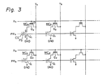
- Figure 3 depicts a circuit diagram of a conventional memory comprised of memory cells MC shown in Figure 2.
- the members having identical reference symbols are substantially the same as those of Figure 2.
- a write operation is achieved as follows. If the memory cell MC a is accessed, a positive high voltage, such as +18 V, is applied to the column line Y a and simultaneously a positive high voltage, such as +20 V is applied to the row line X a and thereby the selecting transistor Q 2 of the specified memory cell MC a is turned to ON. At the same time, a positive high voltage is applied to the drain D of the transistor Q 1 and zero voltage is applied to the control gate CG.
- a positive high voltage such as +18 V
- half-selected memory cells such as MC b , MC c and so on, and non-selected memory cells, such as MC d and so on, exist at the same time, other than selected memory cell MC a .
- a half-selected memory cell is a cell for which the corresponding column line Y is selected, but, the corresponding row line X is not selected, or, alternately, the corresponding row line X is selected, but, the corresponding column line Y is not selected. When both the column and row lines are not selected, the corresponding cell is said to be non-selected.
- the above-mentioned problem may often occur in the half-selected memory cells, especially the half-selected memory cells defined by the row line X a and the column lines other than the column line Y a , i.e. the memory cells other than MC a arranged along the row line X a shown in Figure 3.
- the half-selected memory cells not only the word line X a but also the program line PR a are selected. Therefore, the corresponding transistors Q 2 of the half-selected memory cells are turned ON.
- the above-mentioned undesired erasing may be prevented by employing an additional transistor which acts to disconnect the source S from the ground GND, selectively.
- this solution is not perfect in preventing all the undesired erasing.
- the important matter is to pay attention to the existence of a parasitic capacitor formed between the drain D and the substrate SUB (refer to the parasitic capacitor PC shown in Figure 2).
- the capacitance value of the capacitor PC is considerably large.
- the capacitance value of the capacitor PC may further be increased, because a parasitic capacitor, formed between the substrate SUB and the source S, is also added to the parasitic capacitor PC of the drain D.
- the drain D Since the drain D is provided with a large parasitic capacitor, the voltage level at the drain D cannot change at high speed. Accordingly, the voltage level at the drain D cannot increase at high speed when the positive high voltage V H is applied to the control gate CG. In other words, although the voltage level at the gate CG and also the gate FG changes sharply, the voltage level at the drain D cannot change so sharply. Therefore, a condition, corresponding to the erase operation, is unnecessarily satisfied in a moment during the term in which the voltage level at the drain D follows toward the positive high voltage level at the gate CG and saturates the corresponding positive high voltage level. Although such undesired erasing occurs in a very short time, if such undesired erasing occurs many times repeatedly, the stored data will completely be erased from the floating gate FG, which is one of the previously mentioned defects of the prior art.
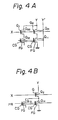
- FIG 4A depicts an equivalent circuit diagram of each memory cell MC according to the present invention
- Figure 4B depicts an equivalent circuit diagram of prior art memory cell MC such as disclosed in US 4,208,158.
- each programming transistor Q 1 of Figures 2 and 3 is depicted as a single transistor element, in its actual arrangement each of the transistors Q 1 is divided into a first transistor Q 11 , acting as a read transistor, having the thick insulation layer IS" and a second transistor Q 12 , acting as a write-erase transistor, having a partially thin insulation layer IS'.
- the selecting transistor Q 2 of Figure 2 or 3 is also divided into a first selecting transistor Q 21 which is connected in series with the read transistor Q 11 , as usual, and a second selecting transistor Q 22 which is connected in series with the write-erase transistor Q, 2 .
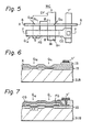
- Figure 5 illustrates a plan view of a memory cell having the circuit diagram of Figure 4A, according to the present invention.
- the reference symbol DF denotes a diffusion area.
- the construction of the memory cell MC shown in Figure 5 will be clarified with reference to Figures 6, 7, 8 and 9. Which are cross-sectional view of the memory cell shown in Figure 5 taken along the line 6-6, 7-7, 8-8 and 9-9 respectively.
- the programming transistor Q, of Figure 3 is divided into the read transistor Q " and the write-erase transistor Q 12 .
- the selecting transistor Q 2 of Figure 3 is also divided into the first selecting transistor Q 2 , and the second selecting transistor Q 22 .
- the diffusion area DF contains n +- type impurities therein (see Figures 8 and 9).
- the diffusion area DF is electrically connected to the column line Y (see Figure 5).
- the diffusion area DF is formed to be a U-shaped area, as seen from Figure 5.
- the two gates X and CG traverse across and over the diffusion area DF so as to form four transistors Qn-Q22 at respective cross portions.
- channels are created at respective transistors Q 11 ⁇ Q 22 .
- an n-type depletion region is formed.
- the drain D of the transistor Q 12 is shorted with the source S of the transistor Q 22 , as seen from the area D(S) of Figure 9.
- the floating gate FG of the transistor Q 12 is provided with a relatively thin insulation layer IS' thereunder, but, other floating gates are provided with the relatively thick insulation layer IS", as seen from Figures 8 and 9. This insulation layer IS' is thin enough to create the tunnel effect.
- the impurity density of the substrate, located under the floating gate FG may not be the same as that of the drain D thereof, alternately, that impurity density may be a value which enables creation of a full depletion state of this transistor, even though electron charges are fully injected into that gate FG.
- the program line PR is arranged in parallel with the row line X
- the program line is distributed perpendicular to the row line X and at the same time in parallel with the column line Y, as the program line Y', which may be clarified with reference to Figures 4A and 5.
- the program line Y' is commonly connected to the control gate CG of each memory cells MC which cells are arranged in parallel with the column line Y. Any desired one of the program line Y' too can be selected by means of a usual decoder circuit which selects any desired one of the column lines (Y).
- the write and erase operations will be clarified with reference to Figure 10.
- Figure 10 illustrates a memory circuit diagram comprised of many memory cells according to the present invention such as shown in Figures 5 through 9.
- the write-erase transistor Q 12 is fabricated in a small size, and therefore, the parasitic capacitor (refer to PC in Figure 2) formed between the drain D of the transistor Q 12 and the substrate can also be very small in area. Consequently, the voltage level developed at the drain D of the write-erase transistor Q 12 can quickly follow the change of the voltage level developed at the control gate CG.
- the parasitic capacitor PC of the prior art is considerably large, undesired erase operation is often performed. Thus, no injection of the electron charges into the floating gate FG is expected in the half-selected memory cells. Further, no injection of the electron charges into the floating gate FG is expected in the non-selected memory cells.
- the selected memory cell MC stores the logic "0" (electron charges are held at the floating gate FG thereof), the voltage level of the floating gate FG is negative, and therefore the threshold level of the selected transistor Q 11 is increased. Thus, the transistor Q 11 is left in normal-OFF state. In this case, no current flows from the column line Y to the ground GND via the transistors Q 21 and Q 11 .
- the stored data "1" or “0” is read from each memory cell.
- the voltage level at the control gate CG is not restricted to the above-mentioned zero voltage, but may be a suitable positive voltage level which is predetermined, for an erase operation and a write operation, according to the respective threshold levels of the memory cells.
- the following table I shows the voltage level to be supplied at the row line X, the program line Y' and the column line Y, in each of the read (READ), the write (WRITE), the partial-erase (PARTIAL ERASE) and the whole-erase (WHOLE ERASE) operations, with respect to the selected memory cell MC s , the half-selected memory cell MC Hsx having the selected row line X only, the half-selected memory cell MC HSY having the selected column line Y only and the non-selected memory cell MC non .
- V 1 denotes the positive high voltage higher than the ordinary power supply voltage level of V cc
- V 2 denotes a read voltage level at the line Y'
- V 3 a read voltage level at the line Y
- V 4 a suitable read voltage level at the row line X.
- the memory circuit device of the present invention is suitable for mass-production. This is because, if a slight error occurs in the location, with respect to the diffusion area DF, of the row line X, the control gate CG or the floating gate FG, in the vertical and/or horizontal directions in the drawing of Figure 5, such a locational error does not cause a significant defect in the manufactured memory cells, due to the presence of the U-shaped diffusion area DF.
- Figure 11 illustrates a plan view showing another embodiment of the memory cell according to the present invention. This figure corresponds to Figure 5 showing the first embodiment according to the present invention.
- the memory cell of Figure 11 differs from that of Figure 5 essentially by the provision of a third selecting transistor Q 3 and an additional program line Y" are newly introduced therein.
- the third selecting transistor Q 3 cooperates with the second selecting transistor Q 22 .
- the previously mentioned program line PR ( Figure 2) is composed of the first program line Y' and the second program line Y".
- the second program line Y" is coupled to the gate G of the third selecting transistor Q 3 .
- the channel of the transistor Q 3 is also formed inside the U-shaped diffusion area DF.
- the first program line Y' is arranged in parallel with the row line X.
- the second program line Y" is arranged in parallel with the column line Y.
- the line Y" is selected by means of the decoder circuit, usually used for selecting a desired one of the column lines Y.
- Figure 12 illustrates a memory circuit diagram comprised of many memory cells according to said another embodiment of the present invention.
- only two column lines are illustrated as Ym and Y n
- only two row lines are illustrated as X and X j
- only two first program lines are illustrated as Y' i and Y' j
- only two second program lines are illustrated as Y" m and Y" n
- only four memory cells are illustrated as MC' im ,MC' in , MC' jm and MC' jn .
- each memory cells (MC) the locations of the transistors (Q 22 , Q 12 , Q 3 ) and (Q 21 , Q 11 ) are reversed with respect to the locations thereof shown in Figure 11, so as to simplify the illustration of the wiring diagram.
- the first, second and third selecting transistors Q 21 , Q 22 and Q 3 are turned to ON and at the same time the positive high voltage is applied to each drain D of the read and write-erase transistors Q 11 and Q 12 .
- the read operation of the memory shown in Figure 12 is substantially the same as that of Figure 10.
- the first program lines Y' i , Y' j ... of Figure 12 should be supposed to be the program lines Y' m , Y' n ... of Figure 10.
- the second program line Y" m , Y" ... of Figure 12 can be in free states during the read operation, that is the voltage level of these lines Y" m , Y" n may be a high voltage or a low voltage level.
- operations of the memory shown in Figure 12 are classified as represented by the following Table II. Table II corresponds to the previously cited Table I.
Description
- The present invention relates to a nonvolatile memory, and more particularly relates to a nonvolatile semiconductor EE-PROM (Electrically Erasable-Programmable Read-Only Memory) of the type comprising a plurality of memory cells and a plurality of column lines and program lines which cooperate with the memory cells, each memory cell comprising a selecting transistor and a programming transistor connected in series with the selecting transistor and comprised of a read transistor having a control gate and a floating gate provided with a relatively thick insulation layer thereunder, and a write-erase transistor having a control gate and a floating gate provided with, partially, a relatively thin insulation layer thereunder, the control gates being commonly connected and the floating gates being also commonly connected, the selecting transistor having a drain connected to the column line and a gate connected to the row line, and the read and write-erase transistors having their control gates connected to the program lines. A nonvolatile semiconductor EE-PROM of this type is disclosed for example by US-4,203,158.
- Programmable ROMs are widely utilized in, for example, computer-aided data processing systems. Usually, a ROM can be programmed only once, either at the factory or in the field, by electrically fusing of otherwise removing unwanted internal links. Accordingly, the conventional programmable ROM has a defect in that a mistake in the programming cannot be corrected. For the purpose of overcoming this defect, an EPROM (Erasable Programmable ROM) has been proposed and widely utilized. In an EPROM, the stored data can be erased by ultraviolet with appropriate voltage pulses. However, in a conventional EPROM, since ultraviolet light is required for reprogramming the stored data, it is not easy for an operator to freely reprogram the stored data.
- In recent years, a nonvolatile EE-PROM has been proposed, for example, in the publication "Electronics", February 28, 1980 pages 113 through 117, entitled "16-K EE-PROM relies on tunneling for byte-erasable program storage". The EE-PROM is basically comprised of a transistor having a source, a drain, a floating gate and a control gate, in which the floating gate partially includes an area of a very thin insulation layer on the order of a hundred A. Thus, a tunnel effect can be created, via the thin insulation, between the drain and the floating gate, and thereby data, to be stored in each memory cell, is reprogrammed.
- EE-PROMs are very useful for an operator in, for example, computer-aided data processing systems, because, as previously mentioned, he can freely reprogram the stored data can be freely reprogrammed without using ultraviolet light. However, such an EE-PROM circuit of the prior art has the following two defects. Firstly, undesired erasure of data often occurs in some of the half-selected memory cells, as it will be explained in detail hereinafter. Secondly, mass-production of such EE-PROM circuit devices is not relatively easy.
- Therefore, it is an object of the present invention, to provide a nonvolatile memory which can overcome the above-mentioned two defects.
- This object is attained with a nonvolatile memory device as defined at the beginning of this description and wherein, according to the invention, in each of the memory cells the selecting transistor is divided into a first selecting transistor and a second selecting transistor, the first selecting transistor being serially connected with the read transistor and the second selecting transistor being serially connected with the write-erase transistor, and wherein the program lines are arranged substantially in parallel with the column lines in the form of lines intersecting the row lines.
- The present invention will be more apparent from the ensuing description with reference to the accompanying drawings wherein:
- Figure 1 illustrates a cross-sectional view showing a known EE-PROM of a prior art;
- Figure 2 depicts a circuit diagram of a conventional memory cell including the transistor of Figure 1 therein;
- Figure 3 depicts a circuit diagram of a conventional memory comprised of memory cells MC shown in Figure 2;
- Figure 4A depicts an equivalent circuit diagram of each memory cell MC according to the present invention;
- Figure 4B depicts an equivalent circuit diagram of each memory cell LC of the prior art;
- Figure 5 illustrates a plan view of a memory cell having the circuit diagram of Figure 4A, according to the present invention;
- Figure 6 is a cross-sectional view of the memory cell shown in Figure 5 taken along the line 6-6;
- Figure 7 is a cross-sectional view of the memory cell shown in Figure 5 taken along the line 7-7;
- Figure 8 is a cross-sectional view of the memory cell shown in Figure 5 taken along the line 8-8;
- Figure 9 is a cross-sectional view of the memory cell shown in Figure 5 taken along the line 9-9;
- Figure 10 illustrates a memory circuit diagram comprised of many memory cells according to the present invention shown in Figures 5 through 9;
- Figure 11 illustrates a plan view showing another embodiment of the memory cell according to the present invention; and,
- Figure 12 illustrates a memory circuit diagram comprised of many memory cells according to said another embodiment of the present invention.
- Figure 1 illustrates a cross-sectional view showing a known EE-PROM of a prior art. In Figure 1, a basic transistor, especially, a FET (Field Effect Transistor) of the EE-PROM is formed in and on a semiconductor substrate SUB. A source S and a drain D of the transistor are formed therein. On the substrate SUB, a floating gate FG and a control gate CG are formed via an insulation layer (Si02) IS. The floating gate FG partially faces the substrate, especially the drain D, via a very thin insulation layer IS'. The floating gate FG, cooperating with the thin insulation layer IS', is necessary to construct the electrically erasable (EE) memory. When a positive high voltage is applied to the control gate CG, the voltage level of the floating gate FG is also increased by the positive high voltage, due to the presence of a capacitor formed between the gate CG and the gate FG having a relatively thick insulation layer IS". At this time, if the voltage level, to be applied to the drain D, is set at 0 V, an extremely high electric field is created, across the thin insulation layer IS', between the gate FG and the drain D. Then electron charges are injected from the drain D into the floating gate FG, which phenomena provide a tunnel effect. Thereby an erase operation is completed. Contrary to the above, in a write operation, the voltage level of the control gate CG is set at 0 V and the voltage level of the drain D is set at a positive high voltage, and thus the electron charges are injected from the floating gate FG into the drain D.
- Figure 2 depicts a circuit diagram of a conventional memory cell including the transistor of Figure 1 therein. The memory cell MC of Figure 2 is fabricated as a two-transistor cell type memory cell. The memory cell MC is comprised of a programming transistor Q1 which corresponds to the transistor of Figure 1 and a selecting transistor Q2. The symbols D, S, FG and CG denote respectively the aforesaid drain, source, floating gate and control gate. The selecting transistor Q2 is used for accessing the transistor Q, when this memory cell MC is specified by an address signal. The programming transistor Q, functions to store, read and write data alternately. These transistors Q1 and Q2 are connected in series with each other along a column line Y, namely a bit line, and to a ground GND. The gate G of the transistor Q2 is connected to a row line X, namely a word line. The control gate CG of the transistor Q1 is connected to a program line PR which is arranged in parallel with the row line X.
- Figure 3 depicts a circuit diagram of a conventional memory comprised of memory cells MC shown in Figure 2. In Figure 3, the members having identical reference symbols are substantially the same as those of Figure 2. In the memory, a write operation is achieved as follows. If the memory cell MCa is accessed, a positive high voltage, such as +18 V, is applied to the column line Ya and simultaneously a positive high voltage, such as +20 V is applied to the row line Xa and thereby the selecting transistor Q2 of the specified memory cell MCa is turned to ON. At the same time, a positive high voltage is applied to the drain D of the transistor Q1 and zero voltage is applied to the control gate CG. Thus, the electron charges are removed from the floating gate FG and the logic "1" is written in the memory cell MCa. In the memory of Figure 3, half-selected memory cells, such as MCb, MCc and so on, and non-selected memory cells, such as MCd and so on, exist at the same time, other than selected memory cell MCa. A half-selected memory cell is a cell for which the corresponding column line Y is selected, but, the corresponding row line X is not selected, or, alternately, the corresponding row line X is selected, but, the corresponding column line Y is not selected. When both the column and row lines are not selected, the corresponding cell is said to be non-selected. In this case, an undesired write operation cannot be expected, because no positive high voltage is applied to any drain D of the transistor Q1 in each of the memory cells MCb, MCc and MCd - --. It should be noted that the write operation is performed when zero volt is applied to the control gate CG and at the same time the positive high voltage is applied to the drain D.
- While, when a whole-erase operation is required with respect to the memory of Figure 3, firstly, zero volt is applied to all the column lines (Y), secondly, a positive high voltage VH is applied to all the word lines (X), and thirdly, the positive high voltage VH is applied to all the control gates CG, which three conditions are satisfied simultaneously. Thus, the electron charges are injected from the drain D into the floating gate FG in each of the transistors Q,. It should be noted that the write operation is performed when zero volt is applied to the control gate CG and at the same time a positive high voltage is applied to the drain D.
- In the above-mentioned write and whole-erase operations, no problem occurs. However, an undesired erasure may occur when a partial-erase operation is achieved, such as an erase operation with respect to memory cells forming a word of 8 bits. If some word is accessed in the memory, only a plurality of memory cells (MCs) for composing that accessed word must satisfy the aforementioned three conditions, that is, firstly, zero volt is applied to the column lines (Y), secondly, the positive high voltage VH is applied to the word line (X), and thirdly, the positive high voltage VH is applied to the control gates CG. Thus, electron charges are injected from each drain D into the corresponding each floating gate FG in the selected memory cells of that word.
- However, the above-mentioned problem may often occur in the half-selected memory cells, especially the half-selected memory cells defined by the row line Xa and the column lines other than the column line Ya, i.e. the memory cells other than MCa arranged along the row line Xa shown in Figure 3. In such half-selected memory cells, not only the word line Xa but also the program line PRa are selected. Therefore, the corresponding transistors Q2 of the half-selected memory cells are turned ON. Although these transistors Q2 are ON, since the corresponding column lines, except for the line Ya, are left in a floating state, the drains D of the transistors Q1 of the half-selected memory cells are also left in a floating state through the respective transistors Q2 which are now conductive. In this case, although a positive high voltage is applied to the respective control gates CG of the half-selected memory cells, the voltage level of the corresponding drains D are expected to increase toward a high voltage level via a so-called capacitor coupling between each gate FG and each corresponding drain D. Therefore, it is also expected that no high electric field is created between each floating gate FG and each corresponding drain D and, as a result, that no undesired erase operation is achieved in each half-selected memory cell.
- However, during actual operation, the previously mentioned problem occurs, that is, undesired erase operation is achieved in such half-selected memory cells for the following reasons. When a positive high voltage is applied to the control gate CG, the voltage level of the floating gate FG is also increased due to the capacitor coupling therebetween .In this case, a channel between the drain D and the source becomes conductive, because of the positive high voltage. When the channel is conductive, the drain D is not left in the aforesaid floating state but is changed to the same voltage level as that of the source S, which level is 0 V. Consequently, a condition, which is identical to the condition for achieving the erase operation, is satisfied, and thereby undesired erasing occurs in some of the half-selected memory cells, where the electron charges are injected from each drain D to each corresponding floating gate FG.
- The above-mentioned undesired erasing may be prevented by employing an additional transistor which acts to disconnect the source S from the ground GND, selectively. However, this solution is not perfect in preventing all the undesired erasing. The important matter is to pay attention to the existence of a parasitic capacitor formed between the drain D and the substrate SUB (refer to the parasitic capacitor PC shown in Figure 2). To make the matter worse, the capacitance value of the capacitor PC is considerably large. In addition, the capacitance value of the capacitor PC may further be increased, because a parasitic capacitor, formed between the substrate SUB and the source S, is also added to the parasitic capacitor PC of the drain D. Since the drain D is provided with a large parasitic capacitor, the voltage level at the drain D cannot change at high speed. Accordingly, the voltage level at the drain D cannot increase at high speed when the positive high voltage VH is applied to the control gate CG. In other words, although the voltage level at the gate CG and also the gate FG changes sharply, the voltage level at the drain D cannot change so sharply. Therefore, a condition, corresponding to the erase operation, is unnecessarily satisfied in a moment during the term in which the voltage level at the drain D follows toward the positive high voltage level at the gate CG and saturates the corresponding positive high voltage level. Although such undesired erasing occurs in a very short time, if such undesired erasing occurs many times repeatedly, the stored data will completely be erased from the floating gate FG, which is one of the previously mentioned defects of the prior art.
- Regarding one memory, in which a row line X and the corresponding program line PR are activated simultaneously, the control gates CG of the non-selected and half-selected memory cells, especially the half-selected memory cells having non-selected row lines X and selected column lines Y, are not selected (activated), and accordingly no electron charges are injected from the drains D to the respective floating gates FG. As a result, in such memory, above-mentioned undesired erasing cannot be expected to occur. Contrary to the above, regarding another memory in which all the control gates are selected (activated) to be a positive high voltage VH, similar defects will be produced with respect to the half-selected memory cells having selected row lines X and non-selected column lines Y.
- There may be a possibility to eliminate the occurrence of such an undesired erase operation by applying the positive high voltage VH not only to the control gate CG but also to the column line Y being connected to the drain D of the programming transistor Ql. However, such possibility is not realized, because a complicated decoder circuit should be incorporated into the memory circuit. It should be noted that the simple decoder circuit of the prior art is sufficient merely to operate to supply high voltage to the column line Y during the erase operation and to make the column line Y to be in a floating state.
- Figure 4A depicts an equivalent circuit diagram of each memory cell MC according to the present invention, while, Figure 4B depicts an equivalent circuit diagram of prior art memory cell MC such as disclosed in US 4,208,158. Although each programming transistor Q1 of Figures 2 and 3 is depicted as a single transistor element, in its actual arrangement each of the transistors Q1 is divided into a first transistor Q11, acting as a read transistor, having the thick insulation layer IS" and a second transistor Q12, acting as a write-erase transistor, having a partially thin insulation layer IS'.
- One essential point of the present invention resides in that, as seen from Figure 4A, the selecting transistor Q2 of Figure 2 or 3 is also divided into a first selecting transistor Q21 which is connected in series with the read transistor Q11, as usual, and a second selecting transistor Q22 which is connected in series with the write-erase transistor Q,2.
- Figure 5 illustrates a plan view of a memory cell having the circuit diagram of Figure 4A, according to the present invention. In Figures 4A and 5, the members having the same reference symbols are identical. The reference symbol DF denotes a diffusion area. The construction of the memory cell MC shown in Figure 5 will be clarified with reference to Figures 6, 7, 8 and 9. Which are cross-sectional view of the memory cell shown in Figure 5 taken along the line 6-6, 7-7, 8-8 and 9-9 respectively.
- In Figure 5, as previously mentioned with reference to Figure 4A, the programming transistor Q, of Figure 3 is divided into the read transistor Q" and the write-erase transistor Q12. The selecting transistor Q2 of Figure 3 is also divided into the first selecting transistor Q2, and the second selecting transistor Q22. The diffusion area DF contains n+-type impurities therein (see Figures 8 and 9). The diffusion area DF is electrically connected to the column line Y (see Figure 5). The diffusion area DF is formed to be a U-shaped area, as seen from Figure 5. The two gates X and CG traverse across and over the diffusion area DF so as to form four transistors Qn-Q22 at respective cross portions. Under the gates CG, FG and the row line X, channels are created at respective transistors Q11~Q22. Especially, in the channel of the transistor Q12, an n-type depletion region is formed. The drain D of the transistor Q12 is shorted with the source S of the transistor Q22, as seen from the area D(S) of Figure 9. The floating gate FG of the transistor Q12 is provided with a relatively thin insulation layer IS' thereunder, but, other floating gates are provided with the relatively thick insulation layer IS", as seen from Figures 8 and 9. This insulation layer IS' is thin enough to create the tunnel effect. Regarding the transistor O11, the impurity density of the substrate, located under the floating gate FG, may not be the same as that of the drain D thereof, alternately, that impurity density may be a value which enables creation of a full depletion state of this transistor, even though electron charges are fully injected into that gate FG.
- Although, in Figure 2, the program line PR is arranged in parallel with the row line X, the program line is distributed perpendicular to the row line X and at the same time in parallel with the column line Y, as the program line Y', which may be clarified with reference to Figures 4A and 5. The program line Y' is commonly connected to the control gate CG of each memory cells MC which cells are arranged in parallel with the column line Y. Any desired one of the program line Y' too can be selected by means of a usual decoder circuit which selects any desired one of the column lines (Y). The write and erase operations will be clarified with reference to Figure 10. Figure 10 illustrates a memory circuit diagram comprised of many memory cells according to the present invention such as shown in Figures 5 through 9. In Figure 10, only two column lines are illustrated as Ym and Yn, only two row lines are illustrated as X and Xj, only two program lines are illustrated as Y'm and Y'n and only four memory cells are illustrated as MCim, MCin, MCjm and MCjn. Further it should be understood that, in each memory cell (MC), the locations of the transistors (Q22, Q12) and (Q21, Q11) are reversed with respect to the locations thereof shown in Figure 5, so as to simplify the illustration of the wiring diagram of Figure 10. When the write operation is commenced in the selected one, for example MCim, of the memory cells, a positive high voltage is applied to the column line Ym (Ym=VH), zero voltage is applied to the program line Y'm (Y'm=0) and a positive high voltage is applied to the row line Xi (Xi=VH). Accordingly, the first and second selecting transistors Q2, and Q22 are turned to ON and at the same time the positive high voltage is applied to each drain D of the read and write-erase transistor Q" and Q12. In this case, since zero voltage is applied to the control gate CG, the electron charges are removed from the floating gate FG of the transistor Q12 to the drain D thereof. Thus, the write operation is completed. In the above, mentioned case, regarding the non-selected memory cell MCjn and the half-selected memory cells MCin and MCjm, since no positive high voltage VH is applied to any drains of the corresponding transistors Q11 and Q12, an undesired write operation for these non-selected and half-selected memory cells cannot be expected to occur.
- When the whole-erase operation is commenced, zero voltage is applied to all the column lines (Ym, Yn - - -), the positive high voltage VH is applied to all the row lines (Xi, Xj - - -) and the positive high voltage VH is applied to all the program lines (Y'm, Y'n ---) and thereby electron charges are injected from the drain D of each transistor Q12 to the floating gate FG thereof. Thus, the whole-erase operation is completed.
- When the partial-erase operation is commenced, a similar condition as for the above whole-erase operation is satisfied with respect only to the selected memory cell, for example MC,m. That is, zero voltage is applied to the column line Ym, the positive high voltage VH is applied to the program line Y'm and the positive high voltage VH is applied to the row line Xi. In this case, regarding the half-selected memory cell MCin having the selected row line Xi and the non-selected column line Yn, no undesired partial-erase operation is performed in such half-selected memory cell MCin, as in any other similarly half-selected memory cells. This is because, firstly, the corresponding program lines Y'n and so on are not selected, and accordingly the corresponding control gates CG are left in an open state or zero voltage state, in which no undesired erase operation can be expected to occur. Secondly, in the other half-selected memory cells, such as MGjm having the non-selected row line X'j, and the selected column line Ym, the control gates CG cells receive the positive high voltage VH; however, the write-erase transistors Q12 are left in floating state, and accordingly no undesired erase operation can be performed. Thirdly, in the memory cells, the write-erase transistor Q12 is fabricated in a small size, and therefore, the parasitic capacitor (refer to PC in Figure 2) formed between the drain D of the transistor Q12 and the substrate can also be very small in area. Consequently, the voltage level developed at the drain D of the write-erase transistor Q12 can quickly follow the change of the voltage level developed at the control gate CG. As previously mentioned, since the parasitic capacitor PC of the prior art is considerably large, undesired erase operation is often performed. Thus, no injection of the electron charges into the floating gate FG is expected in the half-selected memory cells. Further, no injection of the electron charges into the floating gate FG is expected in the non-selected memory cells.
- In Figure 10, when the read operation is achieved, the positive voltage is applied to both the row and column lines X, Y of the selected memory cell MC. If the selected memory cell MC stores the logic "1" (no electron charges are held at the floating gate FG thereof), the voltage level of the floating gate is positive, and therefore the threshold level of the selected transistor Q" is reduced. Thus, the transistor Q11 is left in the normal-ON state. In this case, current flows from the column line Y to the ground GND via the transistors O21 and Q11, which are now ON.
- Contrary to the above, if the selected memory cell MC stores the logic "0" (electron charges are held at the floating gate FG thereof), the voltage level of the floating gate FG is negative, and therefore the threshold level of the selected transistor Q11 is increased. Thus, the transistor Q11 is left in normal-OFF state. In this case, no current flows from the column line Y to the ground GND via the transistors Q21 and Q11.
- As mentioned above, the stored data "1" or "0" is read from each memory cell. In this case, the voltage level at the control gate CG is not restricted to the above-mentioned zero voltage, but may be a suitable positive voltage level which is predetermined, for an erase operation and a write operation, according to the respective threshold levels of the memory cells.
- The following table I shows the voltage level to be supplied at the row line X, the program line Y' and the column line Y, in each of the read (READ), the write (WRITE), the partial-erase (PARTIAL ERASE) and the whole-erase (WHOLE ERASE) operations, with respect to the selected memory cell MCs, the half-selected memory cell MCHsx having the selected row line X only, the half-selected memory cell MCHSY having the selected column line Y only and the non-selected memory cell MCnon.

- In the above cited Table I, the reference symbol V1 denotes the positive high voltage higher than the ordinary power supply voltage level of Vcc, the reference symbol V2 denotes a read voltage level at the line Y'; V3 a read voltage level at the line Y; and, V4 a suitable read voltage level at the row line X.
- As can be understood from Figures 5 through 9, the memory circuit device of the present invention is suitable for mass-production. This is because, if a slight error occurs in the location, with respect to the diffusion area DF, of the row line X, the control gate CG or the floating gate FG, in the vertical and/or horizontal directions in the drawing of Figure 5, such a locational error does not cause a significant defect in the manufactured memory cells, due to the presence of the U-shaped diffusion area DF.
- Figure 11 illustrates a plan view showing another embodiment of the memory cell according to the present invention. This figure corresponds to Figure 5 showing the first embodiment according to the present invention. In Figures 5 and 11, members referenced by the same reference symbols are substantially the same. The memory cell of Figure 11 differs from that of Figure 5 essentially by the provision of a third selecting transistor Q3 and an additional program line Y" are newly introduced therein. The third selecting transistor Q3 cooperates with the second selecting transistor Q22. In this case, the previously mentioned program line PR (Figure 2) is composed of the first program line Y' and the second program line Y". The second program line Y" is coupled to the gate G of the third selecting transistor Q3. The channel of the transistor Q3 is also formed inside the U-shaped diffusion area DF. The first program line Y' is arranged in parallel with the row line X. The second program line Y" is arranged in parallel with the column line Y. The line Y" is selected by means of the decoder circuit, usually used for selecting a desired one of the column lines Y.
- Figure 12 illustrates a memory circuit diagram comprised of many memory cells according to said another embodiment of the present invention. However, only two column lines are illustrated as Ym and Yn, only two row lines are illustrated as X and Xj, only two first program lines are illustrated as Y'i and Y'j, only two second program lines are illustrated as Y"m and Y"n, and only four memory cells are illustrated as MC'im,MC'in, MC'jm and MC'jn. Further it should be understood that, in each memory cells (MC), the locations of the transistors (Q22, Q12, Q3) and (Q21, Q11) are reversed with respect to the locations thereof shown in Figure 11, so as to simplify the illustration of the wiring diagram.
- In Figure 12, when the column line Ym is selected, the corresponding line Y"m is also selected, and similarly when the column line Y is selected, the corresponding line Y"n is selected.
- When the write operation is commenced, in a selected one, for example MC'lm, of the memory cells, a positive high voltage is applied to the column line Ym (Ym=VH), positive high voltage is applied to the second program line Y"m (Y"m=VH) and a positive high voltage is applied to the row line Xi (Xi=VH). Accordingly, the first, second and third selecting transistors Q21, Q22 and Q3 are turned to ON and at the same time the positive high voltage is applied to each drain D of the read and write-erase transistors Q11 and Q12. In this case, since zero voltage is applied to the control gate CG, the electron charges are removed from the floating gate FG of the transistor Q12 to the drain D thereof. Thus, the write operation is completed. In the above case, regarding the non-selected memory cell such as MC'jn and the half-selected memory cells such as MC'in and MC'jm, since firstly no-positive high voltage VH is applied to the drain of the corresponding transistor Q12 and secondly the corresponding transistors Q22 and Q3 are OFF, an undesired write operation for these non-selected and half-selected memory cells cannot be expected to occur.
- When the whole-erase operation is commenced, zero voltage is applied to all the column lines (Ym, Yn ...), the positive high voltage VH is applied to all the row lines (X,, Xj...), the positive high voltage VH is applied to all the first program lines (Y'i, Y'j ...) and the voltage VH is applied to all the second program lines (Y"m, Y"n ...), and thereby electron charges are injected from the drain D of each transistor Q12 to the floating gate FG thereof. Thus, the whole-erase operation is completed.
- When a partial-erase operation is commenced, a condition similar to the one of the above whole-erase operation is satisfied with respect only to the selected memory cell, for example MC'im. In this case, regarding the half-selected memory cell MC';" having the selected row line Xi and the non-selected column line Yn, the second program line Y"n is also non-selected, and accordingly the transistor Q3 is turned to OFF, and the transistor Q12 of the cell MC'in is in a floating state. Consequently, the voltage level of the drain D of this transistor Q,2 changes together with the voltage level of the control gate CG and also the floating gate FG of the transistor Q12 in the cell MC'in. Thereby, no undesired erase operation can be expected to occur in the half-selected memory cell MC'in.
- Regarding the half-selected memory cell MC'jm having the non-selected row line Xj and the selected column line Ym, since the first program line Y'j is not selected, there is no possibility that electron charges be injected into the floating gate FG of the cell MC'jm. Regarding the non-selected memory cell MC'jn, since the lines Xj, Yn, Y"n and Y'j are not selected, there is also no possibility that electron charges be injected into the floating gate FG of the cell MC'jn. This is why no desired erase operation is achieved in any of the memory cells other than the selected memory cell.
- The read operation of the memory shown in Figure 12 is substantially the same as that of Figure 10. In this case, the first program lines Y'i, Y'j ... of Figure 12 should be supposed to be the program lines Y'm, Y'n ... of Figure 10. The second program line Y"m, Y" ... of Figure 12 can be in free states during the read operation, that is the voltage level of these lines Y"m, Y"n may be a high voltage or a low voltage level. Thus, operations of the memory shown in Figure 12 are classified as represented by the following Table II. Table II corresponds to the previously cited Table I.
Claims (11)
Applications Claiming Priority (4)
| Application Number | Priority Date | Filing Date | Title |
|---|---|---|---|
| JP55166354A JPS6034197B2 (en) | 1980-11-26 | 1980-11-26 | non-volatile memory |
| JP166354/80 | 1980-11-26 | ||
| JP55166355A JPS6034198B2 (en) | 1980-11-26 | 1980-11-26 | non-volatile memory |
| JP166355/80 | 1980-11-26 |
Publications (3)
| Publication Number | Publication Date |
|---|---|
| EP0053075A2 EP0053075A2 (en) | 1982-06-02 |
| EP0053075A3 EP0053075A3 (en) | 1983-11-16 |
| EP0053075B1 true EP0053075B1 (en) | 1988-04-20 |
Family
ID=26490755
Family Applications (1)
| Application Number | Title | Priority Date | Filing Date |
|---|---|---|---|
| EP81401837A Expired EP0053075B1 (en) | 1980-11-26 | 1981-11-20 | Nonvolatile memory |
Country Status (3)
| Country | Link |
|---|---|
| EP (1) | EP0053075B1 (en) |
| DE (1) | DE3176713D1 (en) |
| IE (1) | IE53867B1 (en) |
Families Citing this family (5)
| Publication number | Priority date | Publication date | Assignee | Title |
|---|---|---|---|---|
| US4558344A (en) * | 1982-01-29 | 1985-12-10 | Seeq Technology, Inc. | Electrically-programmable and electrically-erasable MOS memory device |
| EP0160720B1 (en) * | 1984-05-07 | 1988-01-07 | Deutsche ITT Industries GmbH | Semiconductor memory cell having an electrically floating memory gate |
| JPH0777078B2 (en) * | 1987-01-31 | 1995-08-16 | 株式会社東芝 | Non-volatile semiconductor memory |
| FR2691289A1 (en) * | 1992-05-15 | 1993-11-19 | Thomson Csf | Field effect semiconductor device, method of making and applying to a matrix-controlled device |
| DE69622973T2 (en) * | 1995-12-07 | 2003-04-24 | Samsung Electronics Co Ltd | Non-volatile memory device |
Citations (1)
| Publication number | Priority date | Publication date | Assignee | Title |
|---|---|---|---|---|
| US4203158A (en) * | 1978-02-24 | 1980-05-13 | Intel Corporation | Electrically programmable and erasable MOS floating gate memory device employing tunneling and method of fabricating same |
Family Cites Families (3)
| Publication number | Priority date | Publication date | Assignee | Title |
|---|---|---|---|---|
| JPS608558B2 (en) * | 1977-03-23 | 1985-03-04 | 日本電気株式会社 | read-only storage |
| US4099196A (en) * | 1977-06-29 | 1978-07-04 | Intel Corporation | Triple layer polysilicon cell |
| DE2743422A1 (en) * | 1977-09-27 | 1979-03-29 | Siemens Ag | Word-wise erasable, non-volatile memory in floating gate technology |
-
1981
- 1981-11-20 DE DE8181401837T patent/DE3176713D1/en not_active Expired
- 1981-11-20 EP EP81401837A patent/EP0053075B1/en not_active Expired
- 1981-11-25 IE IE2759/81A patent/IE53867B1/en not_active IP Right Cessation
Patent Citations (2)
| Publication number | Priority date | Publication date | Assignee | Title |
|---|---|---|---|---|
| US4203158A (en) * | 1978-02-24 | 1980-05-13 | Intel Corporation | Electrically programmable and erasable MOS floating gate memory device employing tunneling and method of fabricating same |
| US4203158B1 (en) * | 1978-02-24 | 1992-09-22 | Intel Corp |
Also Published As
| Publication number | Publication date |
|---|---|
| DE3176713D1 (en) | 1988-05-26 |
| IE53867B1 (en) | 1989-03-29 |
| EP0053075A2 (en) | 1982-06-02 |
| IE812759L (en) | 1982-05-26 |
| EP0053075A3 (en) | 1983-11-16 |
Similar Documents
| Publication | Publication Date | Title |
|---|---|---|
| US5245570A (en) | Floating gate non-volatile memory blocks and select transistors | |
| US4375087A (en) | Electrically erasable programmable read only memory | |
| US6088269A (en) | Compact page-erasable EEPROM non-volatile memory | |
| EP0247875B1 (en) | Block electrically erasable eeprom | |
| US6031765A (en) | Reversed split-gate cell array | |
| US4402064A (en) | Nonvolatile memory | |
| US5812452A (en) | Electrically byte-selectable and byte-alterable memory arrays | |
| US6380636B1 (en) | Nonvolatile semiconductor memory device having an array structure suitable to high-density integrationization | |
| KR100187196B1 (en) | Non-volatile semiconductor memory device | |
| EP0052566A2 (en) | Electrically erasable programmable read-only memory | |
| KR100257661B1 (en) | Non-volatile memory cell structure and process for forming same | |
| EP0463580A2 (en) | Non-volatile semiconductor memory device | |
| KR100461486B1 (en) | Non-volatile semiconductor memory device | |
| KR960016106B1 (en) | Non-volatile semiconductor memory device | |
| JPH03155667A (en) | New architecture for flash erasable eprom memory | |
| EP0637035B1 (en) | Circuit structure for a memory matrix and corresponding manufacturing method | |
| US4766473A (en) | Single transistor cell for electrically-erasable programmable read-only memory and array thereof | |
| US5572464A (en) | Semiconductor memory device and method of using the same | |
| JP2002528840A (en) | Non-volatile memory device and bit line bias method for eliminating program failure in storage device using the same | |
| EP1214715B1 (en) | 1 transistor cell for eeprom application | |
| US4878101A (en) | Single transistor cell for electrically-erasable programmable read-only memory and array thereof | |
| US4379343A (en) | Electrically erasable programmable read-only memory cell having a shared diffusion | |
| EP0053075B1 (en) | Nonvolatile memory | |
| US6011717A (en) | EEPROM memory programmable and erasable by Fowler-Nordheim effect | |
| US6888753B2 (en) | Memory cell array comprising individually addressable memory cells and method of making the same |
Legal Events
| Date | Code | Title | Description |
|---|---|---|---|
| PUAI | Public reference made under article 153(3) epc to a published international application that has entered the european phase |
Free format text: ORIGINAL CODE: 0009012 |
|
| AK | Designated contracting states |
Designated state(s): DE FR GB NL |
|
| PUAL | Search report despatched |
Free format text: ORIGINAL CODE: 0009013 |
|
| AK | Designated contracting states |
Designated state(s): DE FR GB NL |
|
| 17P | Request for examination filed |
Effective date: 19831203 |
|
| GRAA | (expected) grant |
Free format text: ORIGINAL CODE: 0009210 |
|
| AK | Designated contracting states |
Kind code of ref document: B1 Designated state(s): DE FR GB NL |
|
| PG25 | Lapsed in a contracting state [announced via postgrant information from national office to epo] |
Ref country code: NL Effective date: 19880420 |
|
| REF | Corresponds to: |
Ref document number: 3176713 Country of ref document: DE Date of ref document: 19880526 |
|
| ET | Fr: translation filed | ||
| NLV1 | Nl: lapsed or annulled due to failure to fulfill the requirements of art. 29p and 29m of the patents act | ||
| PLBE | No opposition filed within time limit |
Free format text: ORIGINAL CODE: 0009261 |
|
| STAA | Information on the status of an ep patent application or granted ep patent |
Free format text: STATUS: NO OPPOSITION FILED WITHIN TIME LIMIT |
|
| 26N | No opposition filed | ||
| PGFP | Annual fee paid to national office [announced via postgrant information from national office to epo] |
Ref country code: GB Payment date: 19920903 Year of fee payment: 12 |
|
| PGFP | Annual fee paid to national office [announced via postgrant information from national office to epo] |
Ref country code: FR Payment date: 19921127 Year of fee payment: 12 |
|
| PGFP | Annual fee paid to national office [announced via postgrant information from national office to epo] |
Ref country code: DE Payment date: 19930129 Year of fee payment: 12 |
|
| PG25 | Lapsed in a contracting state [announced via postgrant information from national office to epo] |
Ref country code: GB Effective date: 19931120 |
|
| GBPC | Gb: european patent ceased through non-payment of renewal fee |
Effective date: 19931120 |
|
| PG25 | Lapsed in a contracting state [announced via postgrant information from national office to epo] |
Ref country code: FR Effective date: 19940729 |
|
| PG25 | Lapsed in a contracting state [announced via postgrant information from national office to epo] |
Ref country code: DE Effective date: 19940802 |
|
| REG | Reference to a national code |
Ref country code: FR Ref legal event code: ST |