EP0061237B1 - Optical methods for controlling layer thickness - Google Patents
Optical methods for controlling layer thickness Download PDFInfo
- Publication number
- EP0061237B1 EP0061237B1 EP82300920A EP82300920A EP0061237B1 EP 0061237 B1 EP0061237 B1 EP 0061237B1 EP 82300920 A EP82300920 A EP 82300920A EP 82300920 A EP82300920 A EP 82300920A EP 0061237 B1 EP0061237 B1 EP 0061237B1
- Authority
- EP
- European Patent Office
- Prior art keywords
- substrate
- chamber
- layer
- deposition
- thickness
- Prior art date
- Legal status (The legal status is an assumption and is not a legal conclusion. Google has not performed a legal analysis and makes no representation as to the accuracy of the status listed.)
- Expired
Links
Images


Classifications
-
- G—PHYSICS
- G01—MEASURING; TESTING
- G01B—MEASURING LENGTH, THICKNESS OR SIMILAR LINEAR DIMENSIONS; MEASURING ANGLES; MEASURING AREAS; MEASURING IRREGULARITIES OF SURFACES OR CONTOURS
- G01B11/00—Measuring arrangements characterised by the use of optical techniques
- G01B11/02—Measuring arrangements characterised by the use of optical techniques for measuring length, width or thickness
- G01B11/06—Measuring arrangements characterised by the use of optical techniques for measuring length, width or thickness for measuring thickness ; e.g. of sheet material
- G01B11/0616—Measuring arrangements characterised by the use of optical techniques for measuring length, width or thickness for measuring thickness ; e.g. of sheet material of coating
- G01B11/0683—Measuring arrangements characterised by the use of optical techniques for measuring length, width or thickness for measuring thickness ; e.g. of sheet material of coating measurement during deposition or removal of the layer
-
- H—ELECTRICITY
- H01—ELECTRIC ELEMENTS
- H01L—SEMICONDUCTOR DEVICES NOT COVERED BY CLASS H10
- H01L22/00—Testing or measuring during manufacture or treatment; Reliability measurements, i.e. testing of parts without further processing to modify the parts as such; Structural arrangements therefor
- H01L22/10—Measuring as part of the manufacturing process
- H01L22/12—Measuring as part of the manufacturing process for structural parameters, e.g. thickness, line width, refractive index, temperature, warp, bond strength, defects, optical inspection, electrical measurement of structural dimensions, metallurgic measurement of diffusions
Definitions
- the present invention relates to a method and apparatus which may be utilized to mass-produce semiconductor devices, in particular the production of amorphous semiconductor devices by continuous, as opposed to batch, processing.
- Crystalline materials which feature a regular lattice structure were formerly considered essential in the manufacture of reliable semiconductor devices. While solar cells, switches and the like having favorable characteristics continue to be so manufactured, it is recognized that preparation of crystalline materials introduces substantial costs into the semiconductor industry. Single crystal silicon and the like must be produced by expensive and time-consuming methods. Czochralski and like crystal growth techniques involve the growth of an ingot which must then be sliced into wafers and are thus inherently batch processing concepts.
- a method of the kind described is characterised by carrying out the method while advancing the substrate through a deposition chamber in which the layer is deposited on the substrate; analysing the reflected beam to obtain a signal depending on the number of similar extrema in the intensity of light in the wavelength range; comparing the signal with a reference signal corresponding to the desired thickness to produce a error signal; and using the error signal to adjust the parameters controlling the deposition of the layer to tend to cause the desired thickness to be deposited on the moving substrate.
- the invention also includes apparatus for carrying out the above method, the apparatus comprising means for advancing a substrate through a deposition chamber; means for providing a flow of reaction gases to the chamber; means for generating a plasma of the reaction gases in the chamber to cause a uniform deposition of a layer of material on the substrate; means for projecting a beam of light at a variety of wavelengths onto the layer so that substantial portion thereof is reflected; a detector for detecting the reflected beam; means for analysing the reflected beam throughout a range between two wavelengths to obtain a signal depending on the number of similar extrema in the intensity of light in that range resulting from interference at the layer; and means for comparing the signal with a reference signal corresponding to a desired layer thickness to produce an error signal and for using the error signal to vary at least one of the means for advancing the substrate through the chamber, the plasma producing mean, and the means for providing the reaction gas flow to the chamber to tend to cause the desired thickness to be deposited on the moving substrate.
- Figure 1A is a side sectional view of a system, which discloses an "assembly line" for the application of layers of amorphous semiconductor material to a flexible film substrate 10.
- the substrate 10, shown in edge view throughout Figure 1A, comprises a continuous sheet of web-like material, preferably about one to four feet in width.
- the invention is directed in effect to the deposition of a number of layers of amorphous semiconductor material, it represents an intermediate step in the processing of complete semiconductor devices.
- a complete device may additionally include other elements, the application of which requires particularized processing.
- Such processing may occur both prior to the placement of the substrate 10 (as a roll) on a reel 12 of a feed section 14 and subsequent to being gathered into a roll (a plurality of layers of amorphous semiconductor material having been deposited thereon) on a reel 16 of a takeup section 18.
- a flexible metallic foil or metallic surfaced foil is utilized as the substrate 10.
- Certain device configurations may require a thin oxide insulating layer and/or a series of base contacts prior to the application of the layers of amorphous material.
- substrate will be understood to include not only a flexible film, but also elements added thereto by such preliminary processing.
- the intrinsic (material) deposition chamber 30 is considerably longer than either the P-type layer deposition chamber 28 or the N-type layer deposition chamber 32.
- the continuous deposition processes therein require that the substrate 10 travel from reel 12 to reel 16 at substantially constant speed.
- the layer thickness which is a function of the time spent within a given chamber serves, in large measure, to determine the relative lengths of the chambers.
- the exemplary device produced by the system of Figure 1A generally will produce thickness ratios in the range of 10 to 30:1 between the intrinsic and doped layers which occasions an intrinsic chamber of about sixteen feet in length and P- and N-type chambers of about two and one-half feet in length. Again, the manufacture of other devices having differing relative dimensions will dictate, to a large extent, appropriate chamber lengths.
- belt-like masks 34, 36 and 38 each including a plurality of strips (for example one inch wide), may expose corresponding strip-like areas across the width of the substrate 10 as it travels through the chambers 28, 30 and 32.
- the strips 39 which comprise the masks are seen in Figure 1B, a partially sectioned top view of the system of Figure 1A.
- Each of the masks 34, 36 and 38 circulates between a pair of rollers 34', 36' and 38', respectively.
- the pairs of rollers 34', 36' and 38' may be either independently driven or geared to the mechanisms of the reel-to-reel advance which drives the substrate 10 through the system. In either event, appropriate synchronization is maintained between the masks and the traveling substrate 10 to assure proper alignment of the deposited layers.
- the servocontrolled motor drive engaged to the feed reel 12 controls the tension throughout the substrate 10.
- the motor drive 40 engaged to the takeup reel 16 is continually adjustable to provide an optimum rate of travel of the substrate.
- a plurality of paired pinch rollers 42 acts as an edge guide and web-tensioner for the advancing substrate 10.
- the rollers 42 are an optional feature. When utilized, one need not rely upon the natural sag in the substrate 10 but can more reliably adjust the position of the substrate and the mask 36 for proper proximity masking.
- Each of the chambers 28, 30 and 32, through which the substrate 10 is advanced, includes a lamp holder 44 for retaining a plurality of quartz infrared lamps on one side of the substrate 10 and a cathode 46 (for energizing a plasma) on the other side of the substrate 10. It will be seen that the reaction gases enter each chamber through a cathode which additionally includes means for maintaining uniform gas pressure at the surface of the substrate 10.
- a separation valve 48 is located at the entrance and exit of each of the deposition chambers. These valves, discussed in greater detail infra., allow the passage of the continuous substrate and mask from chamber to chamber without contaminating the rection gas environment of each chamber. Control means (not shown in Figure 1A) associated with each of the chambers, will be disclosed with particular reference to Figures 3A and 3B.
- FIGS 2A through 2C are detailed views of one form of a separation valve.
- the valve allows the passage of the traveling substrate 10 into and out of each of the chambers; at the same time, it provides a curtain of inert gas to isolate the gas environment of each chamber from each other chamber. Particularly, contamination of the intrinsic deposition chamber by dopant gases present in the other chamber is prevented, which is essential to the manufacture of a high efficiency device.
- Figure 2A is a front elevation view of a separation valve.
- the valve is formed of a pair of matching manifolds e.g. 50.
- a flange 54 encircles the manifolds when joined together to complete the valve.
- a plurality of holes 56 therein allows the valve to be bolted, riveted or the like to an aperture in either the front or back wall of a chamber.
- a groove 58 is machined into the mating surface of the lower manifold.
- the groove 58 is centrally positioned to form a centrally located slit 60 or opening in the valve when the manifolds are joined together.
- the slit 60 provides communication between a chamber wall and the rest of the system allowing entry and/or exit of the continuously moving substrate 10 (and associated mask if such is employed).
- FIG. 2B a side elevational view in cross-section taken along the line 28-28 of Figure 2A, is provided and one can see that the slit 60 is flared or bevelled to assist the initial threading of the substrate therethrough.
- the opposed (top and bottom) surfaces thereof are coated with teflon or like lubricant.
- An appropriate protective layer of teflon may be provided by spray deposition and subsequent baking at 600 degrees Centigrade.
- the substrate 10 upon passage through the slit 60 is oriented with its active surface facing downward. In this orientation, the valve 48 is located so that the advancing substrate web does not touch the groove 58 at the bottom of the slit 60, but may brush against its opposed side.
- a gas inlet channel 62 provides a communication between a source of inert gas 64 and a cylindrical groove 66 which is at least coextensive with the width of the slit 60.
- This configuration may be seen most readily in Figure 2C which is a top plan view of the valve 48.
- the width of the slit 60 is defined by the distance from the dashed line 68 to the dashed line 70.
- the cylindrical groove 66 one-half of which is formed in the upper manifold 50 and the other half of which is formed in the lower manifold 52, communicates at either end with a gas inlet channel 62 and with a gas outlet channel 72.
- the gas inlet channel 62 is in communication with a source of inert gas 64 whereas the gas outlet channel 72 is connected to a vacuum pump 74.
- the gas source 64 and the vacuum pump 74 interact to maintain the flow of an inert gas, such as argon, within the cylindrical groove 66 at a pressure somewhat greater than the pressure within the deposition chamber. In this manner, a gas curtain is formed in the interior of the valve to prevent cross contamination of the reaction gases and, more important, the entry of dopant gases into the intrinsic deposition chamber. Such dopant gases even in minute amounts can degrade the intrinsic material which would adversely effect cell performance.
- an inert gas such as argon
- Figure 3A is a side elevational view partly in cross section of a deposition chamber 76.
- a controlled environment is maintained at its interior for the glow discharge decomposition process and resultant plasma/substrate equilibrium.
- the chamber is defined by top and bottom walls 78 and 80 riveted or otherwised joined to front and rear walls 82 and 84 and to side walls 86 and 88. All of the walls are preferably of a metal or metallic alloy which is nonreactive with the various gases to be introduced into the chamber.
- the plasma generated by the decomposition of the reaction gases is confined to the area between the cathode 90 (whose potential is regulated by an RF power source 100 to create the required field between the cathode 90 and the grounded substrate 10) and the moving substrate 10, essentially no amorphous material is deposited on the walls of the chamber.
- Slit separation valves 92 and 94 are located in the front and rear walls 82 and 84, respectively, of the chamber 76.
- the valves discussed above, allow passage of the substrate 10 and the plurality of strips which comprise the offset masking 96, if used, through the chamber 76.
- the chamber 76 is idealized in that it contains a full complement of apparatus for controlling the various process parameters including film thickness.
- the chamber 30 of Figure 1A includes means for detecting film thickness of the intrinsic amorphous silicon layer. As previously mentioned, the intrinsic layer is approximately 10 to 30 times as thick as either of the P-type or N-type doped layers. Even though the doped layers are relatively thin, the detection and measurement of the thickness of those layers may also be accomplished.
- the various reaction gases which should include a compound of silicon such as SiF 4 or silane and at least one alterant element such as fluorine or hydrogen which acts to reduce the density of localized states in the energy gap to produce a layer of material having electrical properties which closely resemble crystalline silicon, are introduced into the chamber 76 by means of a reaction gas processor 98.
- the processor 98 includes a supply of appropriate reaction gas and means for evacuating the spent or unreacted gases from the interior of the chamber 76.
- the processor 98 preferably includes scrubbing means and the like for reclamation of the reaction gases.
- the reaction gas processor 98 is coupled to the cathode 90.
- the cathode 90 discussed below, includes unique baffling means so that, in addition to providing an equipotential surface for the formation of a uniform plasma induced by an electric field, it provides a uniform flow of reaction gas across the surface of the substrate and a uniform removal of the spent gases.
- the uniformity of the gas flows assures the deposition of the amorphous material having uniform electrical and optical properties across the surfacd. of the substrate.
- the substrate 10 should be maintained at a fixed potential, as for example, ground potential throughout the system as disclosed herein to allow the formation of an appropriate electrical field between the substrate and the cathode 90.
- a detector 102 is located in the chamber 76.
- the detector 102 may be either an optical pyrometer or a thermocouple supported by a mounting bracket adjacent to the moving substrate.
- the detector 102 has a responsitivity to radiation of about five microns in wavelength and is coupled to servocircuitry 104 which controls a plurality of quartz infrared lamps 106 contained within a lamp holder 108.
- the spacing between the lamps becomes larger as one progresses from the heating region to the constant temperature region through the chamber 76 from entrance to exit. This pattern accomplishes, in a first approximation, the relatively quick heating of the substrate to a desired temperature such as about 300 degrees Centigrade upon entrance into the chamber 76 and its subsequent maintenance thereat for optimum deposition upon exposure to the plasma.
- the infrared detector 102 is chosen for peak sensitivity at a wavelength of about five microns as a result of the fact that such wavelength is the peak where 300 degrees Centigrade obtains maximum radiation.
- the servocircuitry 104 utilizes the radiation pattern for 300 degrees Centigrade to generate an error signal which it then converts to a current to regulate the intensity of the quartz infrared lamps 106 within the lamp holder 108.
- Figure 3B is a cross-sectional view of the chamber 76 taken along line 38-38 of Figure 3A.
- a source of white light 110 is located therein.
- Energy emerging therefrom is projected along optical axis 112 to an optical detector 114 after reflection from the substrate 10
- the optical detector 114 may include focusing optics and a monochrometer.
- the combination of the source 110 and the detector 114 is utilized in the present system to detect the thickness of the layer deposited upon the substrate 10.
- a thickness control circuit 116 accepts the output of the detector, processes the signal through appropriate amplifiers, wave analyzers and the like and then applies the signal to a feedback or servocontrol circuit which operates against a referenced thickness indicator.
- the reference thickness is a function of the particular location of the source/ detector combination along the path of travel of the substrate 10.
- Thickness control circuitry 116 may equivalently include an appropriately programmed microprocessor; in either event, the thickness control circuit 116 derives signals for altering the RF power and/or the speed of the web and/or the valves controlling gas flow upon detection of a thickness which is not appropriate for the stage or location of the detector 114.
- the control of the above-referenced variables is indicated by the multiple outputs of the control circuitry 116; the power source 100 (RF power control); drives of intermediate reels 20, 26 (web speed control); and reaction gas processor 98 (valving).
- the output of the detector 114 is additionally applied to a recorder 118 which includes appropriate circuitry for decoding its output to produce a histogram of thickness so that, in the event portions or segments of the substrate are unusable, they may be easily located, sectioned from the final product, and removed.
- White light is utilized in the thickness detection system, the optical detector and its associated control circuitry are based upon the principle of thin film interference effects. When energy from a source of white light is reflected from a surface, such as the substrate 10, the thickness of the layer from which it is reflected may be determined by comparing the intensity as a function of wavelength of the reflected beam with that of the incident beam. The equation for calculation of the thickness of the deposited film is: where
- a reference is applied to the control circuit 116 corresponding to a desired thickness.
- Circuitry within the thickness control 116 converts the measured reflectance spectrum into a usable error signal which the control 116 continuously drives toward zero by applying corrective signals to any or all of the RF power source 110, the intermediate reel drives 20 and 26 and the reaction gas processor 98.
- the details and design of servocontrol circuitry appropriate for generation of control signals in response to an error signal in the above manner is considered conventional and well known in the electronics and electromechanical arts both in terms of configuration and the elements required.
- FIGS 4A through 4F relate to the cathode 90.
- the cathode 90 serves the dual functions of (1) an electrode for the glow discharge process and (2) a conduit for the flow of fresh reaction gas to and for the evacuation of the spent reaction gas from the plasma region to maintain a uniform, constant pressure glow discharge. It includes a top electrode plate 119 which is electrically connected to the RF power source 100. A plurality of gas inlet openings 120 are uniformly arranged on the electrode plate 119. The openings 120 allow the application of a uniform flow of fresh reaction gas to the surface of the substrate 10 (which serves as the anode of the glow discharge process).
- Uniformly spaced between the gas inlet openings are a plurality of exit vents 122 for collection of spent reaction gases.
- the vents 122 communicate with the vacuum means of the reaction gas processor 98, providing a uniform removal of spent gases from the area between the substrate and the cathode.
- a screen 124 preferably of stainless steel, is associated with each of the exit vents, enhancing the uniformity of exit gas flow by providing a plurality of uniformly spaced openings at the exit vent 122.
- the screen 124 is additionally useful for the collection of solid contaminants.
- the screen 124 is retained between a pair of stainless steel rings 126 and 128.
- An insulating washer 130 surrounds the screen 124 and provides electrical insulation between the rings 126 and 128.
- the screen 124 and the lower ring 128 are grounded, as shown, to a lower baffle member, discussed below.
- the grounding of the - screen isolates the pump out region from the active plasma region between the electrode plate 119 of the cathode 90 and the advancing substrate 10. By grounding these regions, spent reaction gases are evacuated through a dark space so that generation of the plasma is confined to the region between the electrode plate 119 and the substrate 10.
- An insulator such as a sheet of ceramic paper insulation 134 is located adjacent the electrode plate 119.
- a plurality of openings 136 allows the flow of gas therethrough.
- the openings 136 are mated both with the gas inlet openings 120 and the exit vents 122 of the electrode plate 119.
- Gas distribution chambers 137 and 138 are located beneath the top electrode plate 119.
- the chambers 137 and 138 are bounded and formed by top, middle and lower baffle plates 140, 142 and 144, respectively.
- the baffle plates are illustrated in plan view in Figures 4C, 4D and 4E respectively.
- each contains a plurality of holes 146 having cross-section equal to that of the exit vents 122 and arranged thereon so that, when assembled, the holes 146 are aligned with the exit vents 122 of the electrode plate 119.
- the pluralities of holes 148 which serve as gas inlet openings are arranged in various patterns throughout the three baffles 140,142 and 144. The purpose of this deliberate misalignment from baffle to baffle is to assure that inlet gases applied to the chambers 136, 138 will travel an equal distance from a gas inlet 150 to the substrate 10 to equalize the reaction gas pressure across the surface of the substrate 10.
- Reaction gases enter the system through the inlet 150 which communicates with the reaction gas processor 98.
- a donut-shaped chamber 152 accepts the reaction gases and allows their eventual passage into the lower gas distribution chamber 138 through the gas inlet holes 148 of the lower baffle plate 144.
- the reaction gases enter the lower gas distribution chamber, filling it until sufficient pressure causes subsequent flow (through the regularly spaced inlet holes of the middle baffle plate 142) into the upper gas distribution chamber 136.
- the gas remains in the upper chamber 136 until sufficient uniform pressure once again results in its flow (through the holes of the top electrode plate 118) into the area between the cathode 90 and the substrate 10.
- the plasma is generated in and confined to this region by the interaction of the electrical field (imposed between the electrode 110 and the substrate 10) with the reaction gases.
- a portion of the reaction gas is spent or unused during the glow discharge decomposition process.
- Means are provided in the cathode 90 for evacuating this spent gas in a uniform manner so that uniformity of the plasma chemistry over the entire surface area of the substrate is maintained.
- Cylindrical, electrically insulative gas exit ports 154 of ceramic or the like extend the passageway for spent gases from the plasma area through the exit vents 122 and into a vacuum chamber 156.
- the ports 154 are aligned with the gas exit holes 146 of the baffle plates 140, 142 and 144.
- the chamber 156 communicates with the vacuum or pumping means of the reaction gas processor 98 through an exhaust port 158.
- a baffle 160 is provided above the exhaust port 158 to equalize the flow paths of exhaust gases from the exit events 122 to the exhaust port 158 and to minimize any surface pressure differential resulting from the evacuation process. It has been found that, in utilizing a cathode 90, an extremely uniform layer of amorphous material having uniform electrical properties is deposited upon the substrate. It is believed that the fact that all of the reaction gas must travel the same distance from the gas inlet 150 to the gas inlet openings 120 of the electrode plate 119 and that the spent reaction gas travels a substantially uniform distance from the plasma area to the exhaust port 158 assures a uniform, pressure as well as a uniform plasma chemistry at the surface of the substrate 10.
- this uniform pressure and plasma chemistry contribute substantially to the uniform deposition of layers and to the uniform electrical properties such as photoconductivity and dark conductivity of the deposited layers. Such uniformity has not been found to occur when reaction gas is applied, to large area substrates by means of laterally-' spaced manifolds according to the prior art.
- FIG. 4F An alternative embodiment of the cathode is shown in cross-section in Figure 4F.
- the cathode 162 differs from that of Figure 4A by the addition of a chamber 164 for spent gases.
- gas exit ports 166 are seen to extend through the region formerly comprising the vacuum chamber 156.
- Equal flow paths may be obtained in this embodiment by the provision of a plurality of baffles within the chamber having non-aligned holes therein to create subchambers in the manner of the gas distribution chambers 136 and 138 employed to equalize the flow paths of entering reaction gas.
- deposition occurs simultaneously in the chambers 28, 30 and 32 in the plasma regions.
- adhering molecules of reactive gases are removed from the substrate 10 by means of the gas curtain associated with the opening in the chamber separation valves.
- the electrically grounded substrate 10 advances through the plasma region bordered by the substrate and the cathode of the chamber.
- the overall cathode may consist of a plurality of modules identical to those illustrated in Figures 4A through 4F to present a relatively large surface area in the aggregate. This relatively large area. contributes to the uniformity of the layer deposited by reducing the edge effects that often complicate deposition.
- reaction gas including one or more elements or compounds of the alloy to be deposited (such as SiF 4 ) and one or more alterant elements (which may include sensitizers and dopants) is ionized by the field applied between the cathode and the substrate to form the plasma.
- alterant elements which may include sensitizers and dopants
- the rate of deposition of the semiconductor material from the plasma onto the substrate 10 is a function of a number of variables, the control of each of which is closely regulated throughout the system.
- substrate temperature is maintained at between 250 and 300 degrees Centigrade, while the monitoring of layer thickness serves to monitor and control a number of process variables.
- a "low power", "low frequency” plasma generally contributes to depositing alloys of superior performance characteristics. While the technology of layer deposition from a plasma is new and not yet fully understood, it appears that a low kinetic energy of the depositing molecules which is attained in a low power environment favors formation of a deposited structure having the least amount of defects.
- Applicants have developed a number of low power (requiring about.1 watt/cm 2 , as opposed to 1 watt/cm 2 for plasma generation) techniques for use in a system according to the present invention. These techniques generally result in a deposition which produces layers of improved properties and uniformity of thickness and chemical und structural composition.
- resonance phenomena associated with high frequency fields may induce oscillation of electrons within the plasma. Such resonance may prevent the electrons from traveling across the gap between the cathode and the substrate to ionize reaction gases in the vicinity of the substrate.
- a plasma formed of reaction gas interacting with an electric field at 75 kHz possesses uniform color and hence deposits a layer of amorphous material of relatively uniform thickness.
- Layers of quite uniform composition can be obtained from plasmas generated by electric fields in the frequency range of about 50 kHz to about 200 kHz.
- silicon material deposited at 13.56 mHz is characterized by internal tensile stresses, while that deposited in the lower frequency range exhibits reduced internal stresses. Tensile stress is believed to cause the occasional peeling of deposited layers observed in the past. Thus, the structure and adhesion of the layers is enhanced by low frequency, low power deposition techniques.
- the inert gas acts as a kind of intermediate energy buffer to produce a plasma with a profile of energies and species needed for efficient deposition of high quality amorphous Si alloys.
- amorphous is meant an alloy or material which has long range disorder, although it may have short or intermediate order or even contain at times some crystalline inclusions).
- At least one of variables including valving rates, reel drive rates and RF power may be continuously adjusted to self- correct the system in the event of an improper deposition profile.
Description
- The present invention relates to a method and apparatus which may be utilized to mass-produce semiconductor devices, in particular the production of amorphous semiconductor devices by continuous, as opposed to batch, processing.
- Crystalline materials which feature a regular lattice structure were formerly considered essential in the manufacture of reliable semiconductor devices. While solar cells, switches and the like having favorable characteristics continue to be so manufactured, it is recognized that preparation of crystalline materials introduces substantial costs into the semiconductor industry. Single crystal silicon and the like must be produced by expensive and time-consuming methods. Czochralski and like crystal growth techniques involve the growth of an ingot which must then be sliced into wafers and are thus inherently batch processing concepts.
- Recent developments in the field of devices formed of amorphous semiconductor materials offer a potentially significant reduction in production costs. In particular, solar cell technology, which is dependent upon the production of a large number of devices to comprise a panel, is critically affected by processing economies. The feasibility of semiconductor devices produced by amorphous, as opposed to crystalline, materials is disclosed, for example, in US-A-4,217,374 of Ovshinsky and Izu for "Amorphous Semiconductors Equivalent to Crystalline Semiconductors". It has been proposed e.g. in US-A-4226898 to produce a silicon solar cell by successive glow discharge deposition of layers of various conductivities and dopings. Some simple but reliable control of the deposition parameters is desirable to ensure correct layer thickness.
- An article by P. S. Hauge, in the Journal of the Optical Society of America, Vol. 69 No. 8 of August 1979, pages 1143-1152 discloses a method of sensing the thickness of a layer of material deposited on a substrate in the production of a semiconductor device; the method comprising projecting a beam of light onto the layer so that a substantial portion thereof is reflected; detecting the reflected beam; and analysing the reflected beam throughout a range between two wavelengths to obtain a measure of the layer thickness from at least one extremum in the intensity/wavelength curve of the reflected beam resulting from interference at the layer. Such a method is hereinafter referred to as of the kind described. However the particular technique disclosed in the article involves repeated spectrophotometric measurements of light reflected from a finished layer on a stationary substrate and the use of complex algorithms to interpret theoretically the layer thickness from one extremum, the order of which is known, taking account of over or underlying layers. This is impractical for deducing the thickness of a layer being deposited on a moving substrate.
- According to the invention, a method of the kind described is characterised by carrying out the method while advancing the substrate through a deposition chamber in which the layer is deposited on the substrate; analysing the reflected beam to obtain a signal depending on the number of similar extrema in the intensity of light in the wavelength range; comparing the signal with a reference signal corresponding to the desired thickness to produce a error signal; and using the error signal to adjust the parameters controlling the deposition of the layer to tend to cause the desired thickness to be deposited on the moving substrate.
- The invention also includes apparatus for carrying out the above method, the apparatus comprising means for advancing a substrate through a deposition chamber; means for providing a flow of reaction gases to the chamber; means for generating a plasma of the reaction gases in the chamber to cause a uniform deposition of a layer of material on the substrate; means for projecting a beam of light at a variety of wavelengths onto the layer so that substantial portion thereof is reflected; a detector for detecting the reflected beam; means for analysing the reflected beam throughout a range between two wavelengths to obtain a signal depending on the number of similar extrema in the intensity of light in that range resulting from interference at the layer; and means for comparing the signal with a reference signal corresponding to a desired layer thickness to produce an error signal and for using the error signal to vary at least one of the means for advancing the substrate through the chamber, the plasma producing mean, and the means for providing the reaction gas flow to the chamber to tend to cause the desired thickness to be deposited on the moving substrate.
- An example of a continuous layer deposition system according to the invention is illustrated in the accompanying drawings, in which:-
- Figures 1A and 1B are side and top sectional views of the system;
- Figures 2A through 2C are front, cross-sectional and top views respectively of a slit valve for applying an isolation curtain of inert gas at the entrance and exit of each chamber;
- Figures 3A and 3B are side and cross-sectional views of a deposition chamber; and,
- Figures 4A and 4B are top and cross-sectional views of a cathode while Figures 4C through 4E are plan views of the internal baffle plates of the cathode and Figure 4F is an alternative embodiment of the cathode.
- Referring now to the drawings, Figure 1A is a side sectional view of a system, which discloses an "assembly line" for the application of layers of amorphous semiconductor material to a
flexible film substrate 10. Thesubstrate 10, shown in edge view throughout Figure 1A, comprises a continuous sheet of web-like material, preferably about one to four feet in width. As the invention is directed in effect to the deposition of a number of layers of amorphous semiconductor material, it represents an intermediate step in the processing of complete semiconductor devices. A complete device may additionally include other elements, the application of which requires particularized processing. Such processing may occur both prior to the placement of the substrate 10 (as a roll) on areel 12 of afeed section 14 and subsequent to being gathered into a roll (a plurality of layers of amorphous semiconductor material having been deposited thereon) on areel 16 of atakeup section 18. - In the production of solar cells, a flexible metallic foil or metallic surfaced foil is utilized as the
substrate 10. Certain device configurations may require a thin oxide insulating layer and/or a series of base contacts prior to the application of the layers of amorphous material. Thus, for the purpose of this description the term "substrate" will be understood to include not only a flexible film, but also elements added thereto by such preliminary processing. - The
substrate 10, wound through the system of Figure 1A from thefeed reel 12 to thetakeup reel 16 in a generally couterclockwise direction, is additionally guided by means ofintermediate idler reels substrate 10 passes throughchambers feed section 14 and thetakeup section 16, and the like will result in a corresponding rearrangement of the cross section and effect redesign of the device produced. Thus, various devices can be produced in a continuous manner by the present invention wherein other constituents and deposition sequences are employed and such are considered within its scope. - The intrinsic (material)
deposition chamber 30 is considerably longer than either the P-type layer deposition chamber 28 or the N-typelayer deposition chamber 32. The continuous deposition processes therein require that thesubstrate 10 travel fromreel 12 to reel 16 at substantially constant speed. As N-type, intrinsic and P-type layers are continuously deposited on various portions of thetraveling substrate 10, the layer thickness, which is a function of the time spent within a given chamber serves, in large measure, to determine the relative lengths of the chambers. - The exemplary device produced by the system of Figure 1A generally will produce thickness ratios in the range of 10 to 30:1 between the intrinsic and doped layers which occasions an intrinsic chamber of about sixteen feet in length and P- and N-type chambers of about two and one-half feet in length. Again, the manufacture of other devices having differing relative dimensions will dictate, to a large extent, appropriate chamber lengths.
- If masking of the devices is desired, belt-
like masks substrate 10 as it travels through thechambers strips 39 which comprise the masks are seen in Figure 1B, a partially sectioned top view of the system of Figure 1A. Each of themasks substrate 10 through the system. In either event, appropriate synchronization is maintained between the masks and the travelingsubstrate 10 to assure proper alignment of the deposited layers. - An appropriate amount of tension must be maintained within the traveling
substrate 10 for proper registration with themasks substrate 10 or the material deposited thereon. The servocontrolled motor drive engaged to thefeed reel 12 controls the tension throughout thesubstrate 10. Themotor drive 40 engaged to thetakeup reel 16 is continually adjustable to provide an optimum rate of travel of the substrate. - Close proximity contact is desired between the
masks substrate 10. In a common PIN solar cell of the type fabricated by the system of Figure 1A, P- and N-type layers of minute thickness assure that leakage (from separation of mask and substrate) around the strips is likely to be of little significance. The maintenance of relative intimate contact between thesubstrate 10 and themask 36 during intrinsic layer deposition is critical due to the relatively thick intrinsic layer. As seen in Figure 1A, the deposition of intrinsic material occurs in the horizontallyoriented chamber 30. It should be understood that the horizontal disposition of thechamber 30 is not considered critical and that any elevational position desired may be employed. A natural sag occurs in thesubstrate 10, which is also horizontal when it passes therethrough, resulting in a degree of displacement along its length throughout thechamber 30. It has been found that as much as 5/8 of an inch of such sag may occur as it travels through the sixteen-foothorizontal chamber 30. - As shown in Figure 1A, a plurality of paired
pinch rollers 42 acts as an edge guide and web-tensioner for the advancingsubstrate 10. Therollers 42 are an optional feature. When utilized, one need not rely upon the natural sag in thesubstrate 10 but can more reliably adjust the position of the substrate and themask 36 for proper proximity masking. - Each of the
chambers substrate 10 is advanced, includes alamp holder 44 for retaining a plurality of quartz infrared lamps on one side of thesubstrate 10 and a cathode 46 (for energizing a plasma) on the other side of thesubstrate 10. It will be seen that the reaction gases enter each chamber through a cathode which additionally includes means for maintaining uniform gas pressure at the surface of thesubstrate 10. Aseparation valve 48 is located at the entrance and exit of each of the deposition chambers. These valves, discussed in greater detail infra., allow the passage of the continuous substrate and mask from chamber to chamber without contaminating the rection gas environment of each chamber. Control means (not shown in Figure 1A) associated with each of the chambers, will be disclosed with particular reference to Figures 3A and 3B. - Figures 2A through 2C are detailed views of one form of a separation valve. The valve allows the passage of the
traveling substrate 10 into and out of each of the chambers; at the same time, it provides a curtain of inert gas to isolate the gas environment of each chamber from each other chamber. Particularly, contamination of the intrinsic deposition chamber by dopant gases present in the other chamber is prevented, which is essential to the manufacture of a high efficiency device. - Figure 2A is a front elevation view of a separation valve. The valve is formed of a pair of matching manifolds e.g. 50. A
flange 54 encircles the manifolds when joined together to complete the valve. A plurality ofholes 56 therein allows the valve to be bolted, riveted or the like to an aperture in either the front or back wall of a chamber. Agroove 58 is machined into the mating surface of the lower manifold. Thegroove 58 is centrally positioned to form a centrally located slit 60 or opening in the valve when the manifolds are joined together. The slit 60 provides communication between a chamber wall and the rest of the system allowing entry and/or exit of the continuously moving substrate 10 (and associated mask if such is employed). - Turning to Figure 2B, a side elevational view in cross-section taken along the line 28-28 of Figure 2A, is provided and one can see that the slit 60 is flared or bevelled to assist the initial threading of the substrate therethrough. To further protect the substrate from harm or degradation as it passes through the slit 60, the opposed (top and bottom) surfaces thereof are coated with teflon or like lubricant. An appropriate protective layer of teflon may be provided by spray deposition and subsequent baking at 600 degrees Centigrade. In the system of Figures 2A and 2B, the
substrate 10, upon passage through the slit 60, is oriented with its active surface facing downward. In this orientation, thevalve 48 is located so that the advancing substrate web does not touch thegroove 58 at the bottom of the slit 60, but may brush against its opposed side. - A
gas inlet channel 62 provides a communication between a source ofinert gas 64 and acylindrical groove 66 which is at least coextensive with the width of the slit 60. This configuration may be seen most readily in Figure 2C which is a top plan view of thevalve 48. The width of the slit 60 is defined by the distance from the dashedline 68 to the dashedline 70. Thecylindrical groove 66, one-half of which is formed in theupper manifold 50 and the other half of which is formed in the lower manifold 52, communicates at either end with agas inlet channel 62 and with agas outlet channel 72. As referenced above, thegas inlet channel 62 is in communication with a source ofinert gas 64 whereas thegas outlet channel 72 is connected to avacuum pump 74. - The
gas source 64 and thevacuum pump 74 interact to maintain the flow of an inert gas, such as argon, within thecylindrical groove 66 at a pressure somewhat greater than the pressure within the deposition chamber. In this manner, a gas curtain is formed in the interior of the valve to prevent cross contamination of the reaction gases and, more important, the entry of dopant gases into the intrinsic deposition chamber. Such dopant gases even in minute amounts can degrade the intrinsic material which would adversely effect cell performance. - While isolation of the interior of the chamber is the prime' object of the
valve 48, a significant amount of inert gas within the chamber can interfere with the deposition process. For this reason, the gas pressure within thecylindrical groove 66 is maintained only slightly above that of the chamber (about 1 Torr). Impedance to the escape of the inert gas into the chamber is increased as the length (along the direction of travel) of the narrow portion of the slit 60 (seen best in Figure 2B) is increased. Thus, the design of the cross-section of the slit 60 in accordance therewith will serve to minimize the escape of the inert gas from thegroove 66 into the interior of a chamber. - Figure 3A is a side elevational view partly in cross section of a
deposition chamber 76. A controlled environment is maintained at its interior for the glow discharge decomposition process and resultant plasma/substrate equilibrium. The chamber is defined by top andbottom walls rear walls side walls 86 and 88. All of the walls are preferably of a metal or metallic alloy which is nonreactive with the various gases to be introduced into the chamber. As the plasma generated by the decomposition of the reaction gases is confined to the area between the cathode 90 (whose potential is regulated by anRF power source 100 to create the required field between thecathode 90 and the grounded substrate 10) and the movingsubstrate 10, essentially no amorphous material is deposited on the walls of the chamber. -
Slit separation valves rear walls chamber 76. The valves, discussed above, allow passage of thesubstrate 10 and the plurality of strips which comprise the offset masking 96, if used, through thechamber 76. - As the
substrate 10 passes through thechamber 76, the deposition process is closely regulated on a continuous basis. That is, the essential variables of the production process, and the resulting product, are continually monitored and fed back to various corrective controls. Thechamber 76 is idealized in that it contains a full complement of apparatus for controlling the various process parameters including film thickness. Thechamber 30 of Figure 1A, for example, includes means for detecting film thickness of the intrinsic amorphous silicon layer. As previously mentioned, the intrinsic layer is approximately 10 to 30 times as thick as either of the P-type or N-type doped layers. Even though the doped layers are relatively thin, the detection and measurement of the thickness of those layers may also be accomplished. - The various reaction gases, which should include a compound of silicon such as SiF4 or silane and at least one alterant element such as fluorine or hydrogen which acts to reduce the density of localized states in the energy gap to produce a layer of material having electrical properties which closely resemble crystalline silicon, are introduced into the
chamber 76 by means of a reaction gas processor 98. The processor 98 includes a supply of appropriate reaction gas and means for evacuating the spent or unreacted gases from the interior of thechamber 76. In addition, the processor 98 preferably includes scrubbing means and the like for reclamation of the reaction gases. - The reaction gas processor 98 is coupled to the
cathode 90. Thecathode 90, discussed below, includes unique baffling means so that, in addition to providing an equipotential surface for the formation of a uniform plasma induced by an electric field, it provides a uniform flow of reaction gas across the surface of the substrate and a uniform removal of the spent gases. The uniformity of the gas flows assures the deposition of the amorphous material having uniform electrical and optical properties across the surfacd. of the substrate. Thesubstrate 10 should be maintained at a fixed potential, as for example, ground potential throughout the system as disclosed herein to allow the formation of an appropriate electrical field between the substrate and thecathode 90. - A
detector 102 is located in thechamber 76. Thedetector 102 may be either an optical pyrometer or a thermocouple supported by a mounting bracket adjacent to the moving substrate. Thedetector 102 has a responsitivity to radiation of about five microns in wavelength and is coupled to servocircuitry 104 which controls a plurality of quartzinfrared lamps 106 contained within alamp holder 108. The spacing between the lamps becomes larger as one progresses from the heating region to the constant temperature region through thechamber 76 from entrance to exit. This pattern accomplishes, in a first approximation, the relatively quick heating of the substrate to a desired temperature such as about 300 degrees Centigrade upon entrance into thechamber 76 and its subsequent maintenance thereat for optimum deposition upon exposure to the plasma. Theinfrared detector 102 is chosen for peak sensitivity at a wavelength of about five microns as a result of the fact that such wavelength is the peak where 300 degrees Centigrade obtains maximum radiation. The servocircuitry 104 utilizes the radiation pattern for 300 degrees Centigrade to generate an error signal which it then converts to a current to regulate the intensity of the quartzinfrared lamps 106 within thelamp holder 108. - Figure 3B is a cross-sectional view of the
chamber 76 taken along line 38-38 of Figure 3A. One can see that a source ofwhite light 110 is located therein. Energy emerging therefrom is projected alongoptical axis 112 to anoptical detector 114 after reflection from thesubstrate 10 Theoptical detector 114 may include focusing optics and a monochrometer. - The combination of the
source 110 and thedetector 114 is utilized in the present system to detect the thickness of the layer deposited upon thesubstrate 10. Although only one paired source-and-detector combination is shown in Figure 3B, one can see from Figure 3A that a plurality of detector/source combinations is envisioned in the present invention. Eachdetector 114 is engaged to athickness control circuit 116. Thecircuit 116 accepts the output of the detector, processes the signal through appropriate amplifiers, wave analyzers and the like and then applies the signal to a feedback or servocontrol circuit which operates against a referenced thickness indicator. The reference thickness is a function of the particular location of the source/ detector combination along the path of travel of thesubstrate 10.Thickness control circuitry 116 may equivalently include an appropriately programmed microprocessor; in either event, thethickness control circuit 116 derives signals for altering the RF power and/or the speed of the web and/or the valves controlling gas flow upon detection of a thickness which is not appropriate for the stage or location of thedetector 114. The control of the above-referenced variables is indicated by the multiple outputs of thecontrol circuitry 116; the power source 100 (RF power control); drives ofintermediate reels 20, 26 (web speed control); and reaction gas processor 98 (valving). - The output of the
detector 114 is additionally applied to a recorder 118 which includes appropriate circuitry for decoding its output to produce a histogram of thickness so that, in the event portions or segments of the substrate are unusable, they may be easily located, sectioned from the final product, and removed. White light is utilized in the thickness detection system, the optical detector and its associated control circuitry are based upon the principle of thin film interference effects. When energy from a source of white light is reflected from a surface, such as thesubstrate 10, the thickness of the layer from which it is reflected may be determined by comparing the intensity as a function of wavelength of the reflected beam with that of the incident beam. The equation for calculation of the thickness of the deposited film is: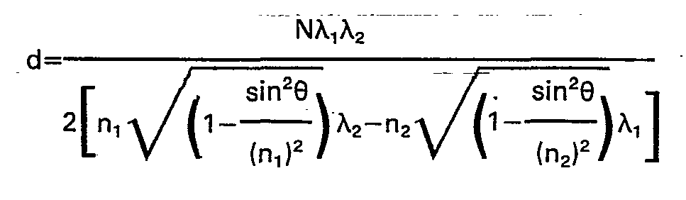
- d=layer thickness
- N=number of similar extrema of intensity displacing wavelength X, from A2
- λ↑ X2=wavelengths at chosen extrema of intensity
- n1 n2=index of refraction of layer material
- 8=angle of incidence of wavelength λ↑ and À2
- A reference is applied to the
control circuit 116 corresponding to a desired thickness. Circuitry within thethickness control 116 converts the measured reflectance spectrum into a usable error signal which thecontrol 116 continuously drives toward zero by applying corrective signals to any or all of theRF power source 110, the intermediate reel drives 20 and 26 and the reaction gas processor 98. The details and design of servocontrol circuitry appropriate for generation of control signals in response to an error signal in the above manner is considered conventional and well known in the electronics and electromechanical arts both in terms of configuration and the elements required. - Figures 4A through 4F relate to the
cathode 90. Thecathode 90 serves the dual functions of (1) an electrode for the glow discharge process and (2) a conduit for the flow of fresh reaction gas to and for the evacuation of the spent reaction gas from the plasma region to maintain a uniform, constant pressure glow discharge. It includes atop electrode plate 119 which is electrically connected to theRF power source 100. A plurality ofgas inlet openings 120 are uniformly arranged on theelectrode plate 119. Theopenings 120 allow the application of a uniform flow of fresh reaction gas to the surface of the substrate 10 (which serves as the anode of the glow discharge process). - Uniformly spaced between the gas inlet openings are a plurality of exit vents 122 for collection of spent reaction gases. The
vents 122 communicate with the vacuum means of the reaction gas processor 98, providing a uniform removal of spent gases from the area between the substrate and the cathode. Ascreen 124, preferably of stainless steel, is associated with each of the exit vents, enhancing the uniformity of exit gas flow by providing a plurality of uniformly spaced openings at theexit vent 122. Thescreen 124 is additionally useful for the collection of solid contaminants. - The
screen 124 is retained between a pair of stainless steel rings 126 and 128. An insulatingwasher 130 surrounds thescreen 124 and provides electrical insulation between therings screen 124 and thelower ring 128 are grounded, as shown, to a lower baffle member, discussed below. The grounding of the - screen isolates the pump out region from the active plasma region between theelectrode plate 119 of thecathode 90 and the advancingsubstrate 10. By grounding these regions, spent reaction gases are evacuated through a dark space so that generation of the plasma is confined to the region between theelectrode plate 119 and thesubstrate 10. - An insulator such as a sheet of
ceramic paper insulation 134 is located adjacent theelectrode plate 119. A plurality ofopenings 136 allows the flow of gas therethrough. Theopenings 136 are mated both with thegas inlet openings 120 and the exit vents 122 of theelectrode plate 119.Gas distribution chambers top electrode plate 119. Thechambers lower baffle plates electrode plate 119. On the other hand, one may observe that the pluralities ofholes 148 which serve as gas inlet openings are arranged in various patterns throughout the three baffles 140,142 and 144. The purpose of this deliberate misalignment from baffle to baffle is to assure that inlet gases applied to thechambers gas inlet 150 to thesubstrate 10 to equalize the reaction gas pressure across the surface of thesubstrate 10. - Reaction gases enter the system through the
inlet 150 which communicates with the reaction gas processor 98. A donut-shapedchamber 152 accepts the reaction gases and allows their eventual passage into the lowergas distribution chamber 138 through the gas inlet holes 148 of thelower baffle plate 144. In such a manner, the reaction gases enter the lower gas distribution chamber, filling it until sufficient pressure causes subsequent flow (through the regularly spaced inlet holes of the middle baffle plate 142) into the uppergas distribution chamber 136. The gas remains in theupper chamber 136 until sufficient uniform pressure once again results in its flow (through the holes of the top electrode plate 118) into the area between thecathode 90 and thesubstrate 10. The plasma is generated in and confined to this region by the interaction of the electrical field (imposed between theelectrode 110 and the substrate 10) with the reaction gases. - A portion of the reaction gas is spent or unused during the glow discharge decomposition process. Means are provided in the
cathode 90 for evacuating this spent gas in a uniform manner so that uniformity of the plasma chemistry over the entire surface area of the substrate is maintained. Cylindrical, electrically insulativegas exit ports 154 of ceramic or the like extend the passageway for spent gases from the plasma area through the exit vents 122 and into a vacuum chamber 156. Theports 154 are aligned with the gas exit holes 146 of thebaffle plates exhaust port 158. A baffle 160 is provided above theexhaust port 158 to equalize the flow paths of exhaust gases from theexit events 122 to theexhaust port 158 and to minimize any surface pressure differential resulting from the evacuation process. It has been found that, in utilizing acathode 90, an extremely uniform layer of amorphous material having uniform electrical properties is deposited upon the substrate. It is believed that the fact that all of the reaction gas must travel the same distance from thegas inlet 150 to thegas inlet openings 120 of theelectrode plate 119 and that the spent reaction gas travels a substantially uniform distance from the plasma area to theexhaust port 158 assures a uniform, pressure as well as a uniform plasma chemistry at the surface of thesubstrate 10. It is further believed that this uniform pressure and plasma chemistry contribute substantially to the uniform deposition of layers and to the uniform electrical properties such as photoconductivity and dark conductivity of the deposited layers. Such uniformity has not been found to occur when reaction gas is applied, to large area substrates by means of laterally-' spaced manifolds according to the prior art. - An alternative embodiment of the cathode is shown in cross-section in Figure 4F. The
cathode 162 differs from that of Figure 4A by the addition of achamber 164 for spent gases. In addition,gas exit ports 166 are seen to extend through the region formerly comprising the vacuum chamber 156. Equal flow paths may be obtained in this embodiment by the provision of a plurality of baffles within the chamber having non-aligned holes therein to create subchambers in the manner of thegas distribution chambers - In operation, deposition occurs simultaneously in the
chambers substrate 10 by means of the gas curtain associated with the opening in the chamber separation valves. Once within a chamber, the electrically groundedsubstrate 10 advances through the plasma region bordered by the substrate and the cathode of the chamber. The overall cathode may consist of a plurality of modules identical to those illustrated in Figures 4A through 4F to present a relatively large surface area in the aggregate. This relatively large area. contributes to the uniformity of the layer deposited by reducing the edge effects that often complicate deposition. - As the
substrate 10 advances through the plasma region, a uniform flow of fresh reaction gas is directed at it through the top surface which comprises the electrode of the novel cathode. The reaction gas, including one or more elements or compounds of the alloy to be deposited (such as SiF4) and one or more alterant elements (which may include sensitizers and dopants) is ionized by the field applied between the cathode and the substrate to form the plasma. - The rate of deposition of the semiconductor material from the plasma onto the
substrate 10 is a function of a number of variables, the control of each of which is closely regulated throughout the system. As mentioned, substrate temperature is maintained at between 250 and 300 degrees Centigrade, while the monitoring of layer thickness serves to monitor and control a number of process variables. In addition, applicants have found that a "low power", "low frequency" plasma generally contributes to depositing alloys of superior performance characteristics. While the technology of layer deposition from a plasma is new and not yet fully understood, it appears that a low kinetic energy of the depositing molecules which is attained in a low power environment favors formation of a deposited structure having the least amount of defects. - Applicants have developed a number of low power (requiring about.1 watt/cm2, as opposed to 1 watt/cm2 for plasma generation) techniques for use in a system according to the present invention. These techniques generally result in a deposition which produces layers of improved properties and uniformity of thickness and chemical und structural composition.
- It is believed that resonance phenomena associated with high frequency fields (such as the 13.56 mHz commonly employed for sputter and prior art glow discharge deposition) may induce oscillation of electrons within the plasma. Such resonance may prevent the electrons from traveling across the gap between the cathode and the substrate to ionize reaction gases in the vicinity of the substrate.
- The desirability of low power, low frequency generation of the deposition plasma has been empirically investigated by the applicants. They have found that, when a plasma was generated at a frequency of 13.56 mHz, significant plasma color nonuniformity was observed which indicates a lack of uniformity of the chemistry within the plasma region. It is believed that nonuniformity of the plasma color is due to the excitation of different species of the reaction gas at different points. It was observed that at the higher frequency, 13.56 mHz, the plasma color at the position close to the gas inlet was blue whereas the color of the plasma close to the outlet was reddish. A higher deposition rate was observed in the blue region than in the reddish region. In contrast, it has been found that a plasma formed of reaction gas interacting with an electric field at 75 kHz possesses uniform color and hence deposits a layer of amorphous material of relatively uniform thickness. Layers of quite uniform composition can be obtained from plasmas generated by electric fields in the frequency range of about 50 kHz to about 200 kHz.
- In addition to plasma and layer uniformity, it has been observed that silicon material deposited at 13.56 mHz is characterized by internal tensile stresses, while that deposited in the lower frequency range exhibits reduced internal stresses. Tensile stress is believed to cause the occasional peeling of deposited layers observed in the past. Thus, the structure and adhesion of the layers is enhanced by low frequency, low power deposition techniques.
- Applicants have found that the deposition of intrinsic silicon exhibiting very favorable photoluminescence and photoconductivity is enhanced even at the relatively high frequency of 13.56 mHz when a quantity of inert gas such as Ar, Ne or He is introduced into the mixture of reaction gas as a diluent. In particular, favorable results were observed when equal amounts of argon and a mixture of SiF4 and H2 (in their customary ratio of 4-9:1) were combined. Here it is theorized that the energy profile of the plasma is significantly altered by the inclusion of the inert gas. The interaction of the depositing gas with the various energy states of the ionized inert gas could easily enhance the formation of plasma species favorable to the desired deposition. Thus, the inert gas acts as a kind of intermediate energy buffer to produce a plasma with a profile of energies and species needed for efficient deposition of high quality amorphous Si alloys. (By the term "amorphous" is meant an alloy or material which has long range disorder, although it may have short or intermediate order or even contain at times some crystalline inclusions).
- Thus it is seen that there has been brought to the semiconductor processing art a method and apparatus for controlling the thickness of a layer of amorphous material deposited upon an advancing sheet. At least one of variables including valving rates, reel drive rates and RF power may be continuously adjusted to self- correct the system in the event of an improper deposition profile.
This equation applies rigorously at normal incidence.
Claims (5)
Applications Claiming Priority (2)
| Application Number | Priority Date | Filing Date | Title |
|---|---|---|---|
| US24438781A | 1981-03-16 | 1981-03-16 | |
| US244387 | 1981-03-16 |
Publications (2)
| Publication Number | Publication Date |
|---|---|
| EP0061237A1 EP0061237A1 (en) | 1982-09-29 |
| EP0061237B1 true EP0061237B1 (en) | 1986-04-16 |
Family
ID=22922523
Family Applications (1)
| Application Number | Title | Priority Date | Filing Date |
|---|---|---|---|
| EP82300920A Expired EP0061237B1 (en) | 1981-03-16 | 1982-02-23 | Optical methods for controlling layer thickness |
Country Status (3)
| Country | Link |
|---|---|
| EP (1) | EP0061237B1 (en) |
| JP (1) | JPS57162420A (en) |
| DE (1) | DE3270551D1 (en) |
Cited By (1)
| Publication number | Priority date | Publication date | Assignee | Title |
|---|---|---|---|---|
| US7859659B2 (en) | 1998-03-06 | 2010-12-28 | Kla-Tencor Corporation | Spectroscopic scatterometer system |
Families Citing this family (7)
| Publication number | Priority date | Publication date | Assignee | Title |
|---|---|---|---|---|
| JPS59168310A (en) * | 1983-03-02 | 1984-09-22 | エナ−ジ−・コンバ−シヨン・デバイセス・インコ−ポレ−テツド | Method and device for measuring thickness of thin-film |
| GB8606748D0 (en) * | 1986-03-19 | 1986-04-23 | Secr Defence | Monitoring surface layer growth |
| JPH0432268A (en) * | 1990-05-29 | 1992-02-04 | Canon Inc | Continuous manufacture of large area solar cell substrate |
| US5399229A (en) * | 1993-05-13 | 1995-03-21 | Texas Instruments Incorporated | System and method for monitoring and evaluating semiconductor wafer fabrication |
| JPH06349925A (en) * | 1993-06-07 | 1994-12-22 | Mitsubishi Electric Corp | Epitaxial growth layer evaluation method and process evaluation test pattern structure |
| JP2648098B2 (en) * | 1994-07-29 | 1997-08-27 | 日本電気株式会社 | Thin film forming equipment |
| CN104122901A (en) * | 2013-04-28 | 2014-10-29 | 苏州北新矿棉板有限公司 | Sheet material thickness control method |
Citations (2)
| Publication number | Priority date | Publication date | Assignee | Title |
|---|---|---|---|---|
| EP0011723A1 (en) * | 1978-12-04 | 1980-06-11 | International Business Machines Corporation | Process and device for the interferometric measurement of changing film thicknesses |
| EP0017461A1 (en) * | 1979-04-09 | 1980-10-15 | Infrared Engineering Limited | Apparatus for determining the thickness, moisture content or other parameter of a film or coating |
Family Cites Families (5)
| Publication number | Priority date | Publication date | Assignee | Title |
|---|---|---|---|---|
| JPS4931272A (en) * | 1972-03-02 | 1974-03-20 | ||
| GB1425941A (en) * | 1972-03-25 | 1976-02-25 | Coating Filter Design Ltd Seel | Manufacture of coated substrates |
| DE2508305A1 (en) * | 1975-02-26 | 1976-09-02 | Leybold Heraeus Gmbh & Co Kg | Monitoring vapour deposited coatings on lenses - using laser beam passing through gas locks in vacuum deposition chamber |
| US4217374A (en) * | 1978-03-08 | 1980-08-12 | Energy Conversion Devices, Inc. | Amorphous semiconductors equivalent to crystalline semiconductors |
| US4226898A (en) * | 1978-03-16 | 1980-10-07 | Energy Conversion Devices, Inc. | Amorphous semiconductors equivalent to crystalline semiconductors produced by a glow discharge process |
-
1982
- 1982-02-23 EP EP82300920A patent/EP0061237B1/en not_active Expired
- 1982-02-23 DE DE8282300920T patent/DE3270551D1/en not_active Expired
- 1982-03-15 JP JP57040660A patent/JPS57162420A/en active Pending
Patent Citations (2)
| Publication number | Priority date | Publication date | Assignee | Title |
|---|---|---|---|---|
| EP0011723A1 (en) * | 1978-12-04 | 1980-06-11 | International Business Machines Corporation | Process and device for the interferometric measurement of changing film thicknesses |
| EP0017461A1 (en) * | 1979-04-09 | 1980-10-15 | Infrared Engineering Limited | Apparatus for determining the thickness, moisture content or other parameter of a film or coating |
Cited By (2)
| Publication number | Priority date | Publication date | Assignee | Title |
|---|---|---|---|---|
| US7859659B2 (en) | 1998-03-06 | 2010-12-28 | Kla-Tencor Corporation | Spectroscopic scatterometer system |
| US7898661B2 (en) | 1998-03-06 | 2011-03-01 | Kla-Tencor Corporation | Spectroscopic scatterometer system |
Also Published As
| Publication number | Publication date |
|---|---|
| JPS57162420A (en) | 1982-10-06 |
| DE3270551D1 (en) | 1986-05-22 |
| EP0061237A1 (en) | 1982-09-29 |
Similar Documents
| Publication | Publication Date | Title |
|---|---|---|
| US4389970A (en) | Apparatus for regulating substrate temperature in a continuous plasma deposition process | |
| US4545136A (en) | Isolation valve | |
| US4369730A (en) | Cathode for generating a plasma | |
| US4525376A (en) | Optical methods for controlling layer thickness | |
| US4542711A (en) | Continuous system for depositing amorphous semiconductor material | |
| US5846373A (en) | Method for monitoring process endpoints in a plasma chamber and a process monitoring arrangement in a plasma chamber | |
| US4410558A (en) | Continuous amorphous solar cell production system | |
| US5443645A (en) | Microwave plasma CVD apparatus comprising coaxially aligned multiple gas pipe gas feed structure | |
| US7169254B2 (en) | Plasma processing system and apparatus and a sample processing method | |
| US4519339A (en) | Continuous amorphous solar cell production system | |
| US4995341A (en) | Microwave plasma CVD apparatus for the formation of a large-area functional deposited film | |
| JPS6243554B2 (en) | ||
| JPH02148715A (en) | Apparatus for forming semiconductor device continuously | |
| EP0060625B1 (en) | Plasma deposition of amorphous materials | |
| US5129359A (en) | Microwave plasma CVD apparatus for the formation of functional deposited film with discharge space provided with gas feed device capable of applying bias voltage between the gas feed device and substrate | |
| Bruno et al. | rf glow discharge of SiF4‐H2 mixtures: Diagnostics and modeling of the a‐Si plasma deposition process | |
| EP0121340A2 (en) | Method and apparatus for measuring thin film thickness | |
| EP0061237B1 (en) | Optical methods for controlling layer thickness | |
| EP0060651B1 (en) | Apparatus including improved cathode for continuous deposition of amorphous material | |
| US4897284A (en) | Process for forming a deposited film on each of a plurality of substrates by way of microwave plasma chemical vapor deposition method | |
| US5707692A (en) | Apparatus and method for processing a base substance using plasma and a magnetic field | |
| EP0060626B1 (en) | Isolation valve | |
| US5846612A (en) | Process for forming high-quality deposited film utilizing plasma CVD | |
| JP2841243B2 (en) | Deposition film forming apparatus by microwave plasma CVD method | |
| JPH09195055A (en) | Roll-to-roll treatment and apparatus therefor |
Legal Events
| Date | Code | Title | Description |
|---|---|---|---|
| PUAI | Public reference made under article 153(3) epc to a published international application that has entered the european phase |
Free format text: ORIGINAL CODE: 0009012 |
|
| AK | Designated contracting states |
Designated state(s): DE FR GB IT NL |
|
| RAP1 | Party data changed (applicant data changed or rights of an application transferred) |
Owner name: ENERGY CONVERSION DEVICES INC. |
|
| 17P | Request for examination filed |
Effective date: 19830221 |
|
| GRAA | (expected) grant |
Free format text: ORIGINAL CODE: 0009210 |
|
| AK | Designated contracting states |
Kind code of ref document: B1 Designated state(s): DE FR GB IT NL |
|
| ITF | It: translation for a ep patent filed |
Owner name: ING. C. GREGORJ S.P.A. |
|
| REF | Corresponds to: |
Ref document number: 3270551 Country of ref document: DE Date of ref document: 19860522 |
|
| ET | Fr: translation filed | ||
| PLBI | Opposition filed |
Free format text: ORIGINAL CODE: 0009260 |
|
| PLBI | Opposition filed |
Free format text: ORIGINAL CODE: 0009260 |
|
| 26 | Opposition filed |
Opponent name: LEYBOLD - HERAEUS GMBH Effective date: 19861213 |
|
| NLR1 | Nl: opposition has been filed with the epo |
Opponent name: LEYBOLD - HERAEUS GMBH |
|
| PG25 | Lapsed in a contracting state [announced via postgrant information from national office to epo] |
Ref country code: GB Effective date: 19870223 |
|
| 26 | Opposition filed |
Opponent name: BALZERS AKTIENGESELLSCHAFT Effective date: 19870114 |
|
| NLR1 | Nl: opposition has been filed with the epo |
Opponent name: BALZERS AKTIENGESELLSCHAFT. |
|
| GBPC | Gb: european patent ceased through non-payment of renewal fee | ||
| NLV4 | Nl: lapsed or anulled due to non-payment of the annual fee | ||
| RDAG | Patent revoked |
Free format text: ORIGINAL CODE: 0009271 |
|
| STAA | Information on the status of an ep patent application or granted ep patent |
Free format text: STATUS: PATENT REVOKED |
|
| REG | Reference to a national code |
Ref country code: FR Ref legal event code: ST |
|
| 27W | Patent revoked |
Effective date: 19870821 |
|
| GBPR | Gb: patent revoked under art. 102 of the ep convention designating the uk as contracting state |