EP0063886A2 - A method of and a system for pulse communication - Google Patents
A method of and a system for pulse communication Download PDFInfo
- Publication number
- EP0063886A2 EP0063886A2 EP82301861A EP82301861A EP0063886A2 EP 0063886 A2 EP0063886 A2 EP 0063886A2 EP 82301861 A EP82301861 A EP 82301861A EP 82301861 A EP82301861 A EP 82301861A EP 0063886 A2 EP0063886 A2 EP 0063886A2
- Authority
- EP
- European Patent Office
- Prior art keywords
- signal
- mark inversion
- coded mark
- data signal
- transmission
- Prior art date
- Legal status (The legal status is an assumption and is not a legal conclusion. Google has not performed a legal analysis and makes no representation as to the accuracy of the status listed.)
- Granted
Links
Images


Classifications
-
- H—ELECTRICITY
- H04—ELECTRIC COMMUNICATION TECHNIQUE
- H04L—TRANSMISSION OF DIGITAL INFORMATION, e.g. TELEGRAPHIC COMMUNICATION
- H04L25/00—Baseband systems
- H04L25/38—Synchronous or start-stop systems, e.g. for Baudot code
- H04L25/40—Transmitting circuits; Receiving circuits
- H04L25/49—Transmitting circuits; Receiving circuits using code conversion at the transmitter; using predistortion; using insertion of idle bits for obtaining a desired frequency spectrum; using three or more amplitude levels ; Baseband coding techniques specific to data transmission systems
- H04L25/4906—Transmitting circuits; Receiving circuits using code conversion at the transmitter; using predistortion; using insertion of idle bits for obtaining a desired frequency spectrum; using three or more amplitude levels ; Baseband coding techniques specific to data transmission systems using binary codes
- H04L25/4908—Transmitting circuits; Receiving circuits using code conversion at the transmitter; using predistortion; using insertion of idle bits for obtaining a desired frequency spectrum; using three or more amplitude levels ; Baseband coding techniques specific to data transmission systems using binary codes using mBnB codes
- H04L25/491—Transmitting circuits; Receiving circuits using code conversion at the transmitter; using predistortion; using insertion of idle bits for obtaining a desired frequency spectrum; using three or more amplitude levels ; Baseband coding techniques specific to data transmission systems using binary codes using mBnB codes using 1B2B codes
- H04L25/4912—Transmitting circuits; Receiving circuits using code conversion at the transmitter; using predistortion; using insertion of idle bits for obtaining a desired frequency spectrum; using three or more amplitude levels ; Baseband coding techniques specific to data transmission systems using binary codes using mBnB codes using 1B2B codes using CMI or 2-HDB-3 code
Definitions
- the present invention relates to a method of and a system for pulse communication which has a large signal transmission speed and a large transmission capacity and which permits the signal transmission line to be monitored.
- Such a method and system is particularly suitable for communication by the transmission of optical pulses along optical fibres.
- a method of pulse communication between a transmission site and a reception site comprises the steps of:
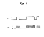
- Figure 1 illustrates the principle of a previously used pulse communication system.
- the previously known pulse communication system operated on a 2-level pulse communication system in which data signals were transmitted as logical 0 and 1 as shown in Figure l(a), or were transmitted as envelope modulations in a pulse communication system in which repetition pulses were subjected to envelope modulation as shown in Figure l(b).
- Fig. 2 shows the principle of the pulse communication method according to the present invention, in which a trans- mission data signal a is converted into a coded mark inversion (CMI) code ⁇ and thereafter modulated into a 3-level CMI signal g and transmitted by the signal transmission line. On the reception side, the received signal is demodulated separately into the data signal and the clock signal.
- CMI coded mark inversion
- 01 of the CMI code ⁇ is corresponded to logical 1 of the transmission data signal a and 11 or 00 of the CMI code ⁇ is corresponded to logical 0 of the transmission data signal a while 10 of the CMI code ⁇ is not corresponded to any of logical.1 and 0 of the transmission data signal Further,.00 and 11 of the CMI code ⁇ are alternatively corresponded to logical 0 of the transmission data signal a.
- the transmission data signal a of frequency fo is sampled at the middle of the signal frequency in synchronism with the rising of the transmission clock signal @ of-frequency 2fo and is converted into the transmission CMI code ⁇ in accordance with the correspondence described above.
- the transmission CMI code ⁇ is converted in synchronism with the rising of a transmission multiplied clock signal a of frequency 4fo into the 3-level CMI signal g to logical 0 and -1 of which logical 1 and 0 of the transmission CMI code are corresponded.
- logical 1 of the transmission data signal a is converted into one negative pulse and one positive pulse of the 3-level CMI signal g in correspondence with the falling and the rising, respectively, of the transmission clock signal.
- logical 0 of the transmission data signal a is converted into two positive pulses or two negative pulses of the 3-level CMI signal g in correspondence with the falling and the rising, respectively, of the transmission clock signal. Since it is so prearranged that logical 0 of the transmission signal is corresponded to 00 and 11 alternatively in conversion into the transmission CMI code ⁇ , the two positive or negative pulses of the 3-level CMI signal g are pulse signals having the signs opposite to two pulse signals used for logical 0 of the transmission data signal a immediately before them. This 3-level CMI signal is transmitted to the reception side through the signal transmission line.
- the probability of occurrence of logical 0 and 1 in the 3-level CMI signal g as a whole is 1:1.
- the average value of the 3-level CMI signal g is half of the peak value (in Fig. 2, it is the half of the maximum value +1 and the minimum value -1, that is 0), to make the level of the transmission signal easily detectable. This characteristic can be utilized as an abnormality monitoring signal of the signal transmission line.
- the abnormality can be detected by comparing the half value level with the predetermined reference value by means of a comparator.
- This characteristic of the system according to the present invention is effective particularly in the optical pulse communication system in which the signal is transmitted by the optical pulse in the optical fiber. Further, since both the positive pulse and the negative pulse of the 3-level CMI signal g are corresponded to the rising or the falling of the transmission clock signal b and since 10 of the transmission CMI code ⁇ is not corresponded to any of logical 0 and 1 of the transmission data signal a, it can be distinguished whether the pulse of the 3-level CMI signal corresponds to the rising or to the falling of the clock signal.
- the pulse communication system can transmit the clock signal with the data signal.
- the transmission data signal a can be demodulated to a reception data signal through reverse steps to the transmission, by corresponding logical 1 of the reception data signal to 01 of the reception CMI code c and corresponding logical 0 of the reception data signal to 00 or 11 of the reception CMI code ⁇ .
- the 3-level CMI signal to be transmitted includes the data signal, the clock signal, and the transmission line monitoring signal.
- the transmission data signal a is transmitted in the multiplied clock frequency 4fo which is four times the frequency fo of the transmission data signal, the necessary transmission band is only four times the signal pulse frequency. That is, one fourth of the transmission band can be used as the data signal.
- reception timing clock signal corresponding to the reception data signal can be easily extracted by a sequence-circuit operated with the clock signal four times the transmission speed without using any complicated circuit such as PLL circuit.
- the reception data signal includes clock information including phase, and the clock information can be easily regenerated by the sequential circuit transiting in the clock frequency twice the transmission speed. Since 10 of the CMI-code is not used as data, another advantage is provided that even if the phase of the clock is shifted 180 degrees with respect to the data signal, it can be corrected.
- 01 of the CMI code is corresponded to logical-Q of the data signal, 11 or 00 of the CMI code are alternatively corresponded to logical 1 of the data signal, and when 10 of the CMI code is not corresponded to any of logical 1 and 0 of the data signal;
- 10 of the CMI code is corresponded to logical 1 of the data signal, 11 and 00 of the CMI code are alternatively corresponded to logical 0 of the data signal, and when 01 of the CMI code is not corresponded to any of logical 1 and 0 of the data signal;
- 10 of the CMI code is corresponded to logical 0 of the data signal, 11 and 00 of the CMI code are alternatively corresponded to logical 1 of the data signal, and 01 of the CMI code is not corresponded to any of logical 1 and 0 of the data signal.
- the positive pulse is corresponded to logical 1 and the negative pulse is corresponded to logical 0, they may be otherwise corresponded, for.example, the negative pulse is corresponded to logical 1 and the positive, pulse is corresponded to logical 0.
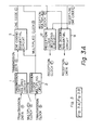
- Figs. 3A and 3B are a block diagram showing a pulse communication system for practising the pulse communication system according to the present invention, comprising a transmission data holding circuit 1, a transmission clock multiplying circuit 2, a CMI coding sequential circuit 3, a modulating circuit 4, a 3-level C M I signal coding circuit 5, a signal transmission line 6, a 3-level CMI signal decoding circuit 7, a demodulating circuit 8, a CMI decoding, sequential circuit 9, a transmission line monitoring circuit 10, a multiplied clock regenerating circuit 11, and a reception clock decoding sequential circuit 12.
- the transmission clock multiplying circuit 2 converts the transmission clock signal b into.the transmission multiplied clock signal d of frequency 4fo which is twice the frequency 2fo and applies the transmission multiplied clock signal d to the transmission data holding circuit 1, the CMI coding sequential circuit 3 and the modulating circuit 4.
- the ⁇ CMI coding sequential circuit 3 converts the transmission data signal a into the transmission CMI code ⁇ .
- the modulating circuit 4 separates the transmission C M I code ⁇ into the transmission positive pulse signal d and the transmission negative pulse signal e which are converted into the 3-level CMI signal g by the 3-level CMI signal coding circuit 5.
- the 3-level CMI signal g is transmitted as an optical signal by a light emitting diode of the 3-level CMI signal coding circuit 5 through the signal transmission line 6 comprising the optical fibers.
- the 3-level CMI signal decoding circuit 7 decodes the 3-level CMI signal of the optical signal into the electrical reception positive pulse signal A and reception negative pulse B which are demodulated into the reception CMI code ⁇ by the demodulating circuit 8.
- the multiplication clock regenerating circuit 11 extracts the reception multiplied clock signal D from the 3- level CMI signal g and applies it to the CMI decoding sequential circuit 9 which converts the reception CMI code c into the reception data signal E and reception clock decoding circuit 12.
- the reception clock decoding sequential circuit.12 converts the reception CMI code ⁇ into the reception clock signal F by the reception multiplied clock signal. By this, the data signal and the clock signal are extracted separately.
- the 3-level C M I signal decoding circuit 7 takes out the average value of the 3-level CMI signal which is the optical signal received thereby, and the transmission line monitoring circuit 10 outputs a transmission line monitoring signal for monitoring the abnormality of the signal transmission line by comparing always the average value with a predetermined value.
- Fig. 4 shows an embodiment of the CMI coding sequential circuit 3 according to the present invention, in which reference numerals 13a and 13b denote data holding flip-flops, and reference numerals 14a and 14b denote JK input type flip-flops.
- the flip-flop 13b holds the transmission data signal a by the transmission multiplied clock signal d
- the flip-flop 13a holds the transmission data signals a sequentially with one clock's delay from the flip-flop 13b by the transmission multiplied clock signal d.
- the outputs of the flip-flops 13a, 13b, 14a and 14b are returned to the JK inputs of the flip-flops 14a and 14b by a combinational circuit to form the CMI coding sequential circuit 3.
- 01 of the transmission CMI code ⁇ is outputted to logical 1 of the transmission data signal a and 00 and 11 of .
- the transmission CMI code ⁇ are alternatively outputted to logical 0 of the transmission data signal a, to thereby make the transmission CMI signal ⁇ as against the transmission data signal a as shown in Fig. 2.
- Fig. 5 shows an embodiment of the modulating circuit 4 according to the present invention, in which the transmission CMI code ⁇ is applied to a 2-input NAND gate 16a and inverted by an inverter 17a into the transmission positive pulse signal e.
- the transmission CMI code ⁇ inverted by an inverter 15 is applied to a 2-input NAND gate 16b and is further inverted by an inverter 17b into the transmission negative pulse signal f.
- Fig. 6 shows an embodiment of the 3-level CMI signal coding circuit 5 according to the present invention, in which the transmission positive pulse signal e and the transmission negative pulse signal f are applied to one inputs of 2-input NAND gates 18a and 18b, respectively, and transmission control ; signals are applied to the other inputs thereof.
- the transmission control signal to decide whether the optical signal is or is not to be transmitted. If the data signal is to be transmitted, the transmission control signal becomes logical 1, and a light emitting diode 19 emits light at the maximum value when the transmission positive pulse signal e is applied and at the minimum value when the transmission negative pulse signal f is applied.
- the transmission control signal In the state where the transmission control signal is logical 1 and yet there is no transmission signal pulse, the light emitting diode 19 emits light at the half value of the maximum value and the minimum value determined by resistors 20 and 21. If the data signal is not to be transmitted, the transmission control signal becomes logical 0 and the light emitting diode 19 is extinguished.
- the transmission data signal a is transmitted by the diode 19 as an optical pulse signal carried through the signal transmission line 6, it will be obvious to those skilled in the art that-another embodiment of the 3-level CMI signal coding circuit 5 for carrying an ordinary electrical pulse signal is easily constructed within the scope of the present invention.
- Fig. 7 shows an emboidment of the 3-level CMI signal decoding circuit 7, in which the 3-level CMI signal g transmitted through the signal transmission line 6 is amplified by a preamplifier 22 and thereafter applied to a positive pulse comparator 24, a negative pulse comparator 25, and a threshold setting circuit 23 generates the half value of the maximum and the minimum value of the transmitted signal as a predetermined threshold value.
- the positive pulse comparator 24 outputs the reception positive pulse signal @when the 3-level CMI signal @is larger than the threshold value and, on the other hand, the negative pulse comparator 25 outputs the reception negative pulse signal B when the 3-level CMI signal g is smaller than the threshold value.
- the transmitted 3-level CMI signal g is applied also to a reception signal average extracting circuit 30 which extracts the average value of the received 3-level CMI signals g.
- the average value is compared by a comparator 31 with a reference value outputted by a reception signal reference setting circuit 29 for distinguishing any abnormality in the signal transmission line, and the comparator 31 outputs a transmission line monitoring signal.
- Fig. 8 shows an embodiment each of the demodulating circuit 8 and the CMI decoding sequential circuit 9 according to the present invention.
- the demodulating circuit 8 is constructed as an RS flip-flop.
- the reception CMI code ⁇ which is the output signal of the RS flip-flop is held sequentially by the reception multiplied clock signal D.
- the data holding flip-flop 27b holds the reception CMI code to the data holding flip-flop 27a one clock later than the reception multiplied clock signal D.
- the CMI decoding sequential circuit 9 formed by returning the outputs of JK input flip-flop 28a and 28b and the outputs of the data holding flip-flops 27a and 27b to the inputs of the JK input flip-flops 28a and 28b by means of a combinational circuit makes, as shown in Fig. 2, the reception data signal E and the reception clock signal F from the reception positive pulse signal A and the reception negative pulse signal
- a pulse communication system which is compact in construction and yet is large both in the signal transmission speed and in the transmission capacity, and further is capable of deciding easily whether absence of a signal pulse is due to any abnormality in the signal transmission line or due to one of the 2-level signal pulses, to thereby monitor the transmission line.
Abstract
Description
- The present invention relates to a method of and a system for pulse communication which has a large signal transmission speed and a large transmission capacity and which permits the signal transmission line to be monitored. Such a method and system is particularly suitable for communication by the transmission of optical pulses along optical fibres.
- In the past pulse communication systems operated on a 2-level pulse communication system in which data signals were transmitted as logical 0's or l!s or were transmitted as envelope modulation of a repetitive pulse signal. Such 2-level pulse communication has a disadvantage that it is unable to determine whether absence of a received signal denotes one of the 2-level states of the received signal and hence one of the data signals or some trouble in the signal transmission line. To overcome this problem a transmission line monitor signal has been inserted in the transmitted stream of high speed pulsed signals, then the 2-level pulse communication system has a further disadvantage that the apparatus has to be large in construction since it has to be able to detect the phase of the received signal accurately. On the other hand, the envelope modulation pulse communication system has a disadvantage in that the signal transmission speed is inevitably lower than the pulse repetition frequency which is the potential maximum signal transmission speed.
- In accordance with a first aspect of this invention a method of pulse communication between a transmission site and a reception site comprises the steps of:
- converting a data signal to be transmitted into a coded mark inversion code in synchronism with a clock signal;
- converting the coded mark inversion code into a 3-level coded mark inversion signal and thereafter transmitting it through a transmission line from the transmission site to the reception site; and
- decoding the 3-level coded mark inversion signal into the coded mark inversion code and thereafter regenerating and recovering the data signal and the clock signal separately at the reception site.
- In accordance with a second aspect of this invention a pulse communication system comprises
- a transmission clock multiplying circuit for multiplying a transmission clock signal to a required frequency;
- a coded mark inversion coding sequential circuit for converting a data signal to be transmitted into a coded mark inversion code;
- a 3-level coded mark inversion signal coding circuit for converting the coded mark inversion code into a 3-level coded mark inversion signal;
- a signal transmission line for transmitting the 3-level coded mark inversion signal from the transmission site to the reception site;
- a 3-level coded mark inversion signal decoding circuit for decoding a received 3-level coded mark inversion signal into a coded mark inversion code;
- a coded mark inversion decoding sequential circuit for decoding the decoded coded mark inversion code into a data signal; and,
- a clock circuit for extracting a multiplied clock signal from the received 3-level coded mark inversion signal and recovering a received clock signal.
- A particular embodiment of the present invention will now be described and contrasted with the prior art with reference to the accompanying drawings; in which:-
- Figures lA and B are diagrams illustrating the principle of conventional pulse communication systems;
- Figure 2 is a series of timing diagrams illustrating the principle of the present invention;
- Figures 3A and 3B are a block diagram showing the embodiment of a pulse communication system in accordance with the present invention;
- Figure 4 is a circuit diagram of an embodiment of a coded mark inversion coding sequential circuit;
- Figure 5 is a circuit diagram of a modulating circuit;
- Figure 6 is a circuit diagram of a 3-level coded mark inversion signal coding circuit;
- Figure 7 is a circuit diagram of a 3-level coded mark inversion decoding circuit; and,
- Figure 8 is a circuit diagram of a demodulating circuit and a coded mark inversion decoding sequential circuit.
- Figure 1 illustrates the principle of a previously used pulse communication system. The previously known pulse communication system operated on a 2-level pulse communication system in which data signals were transmitted as logical 0 and 1 as shown in Figure l(a), or were transmitted as envelope modulations in a pulse communication system in which repetition pulses were subjected to envelope modulation as shown in Figure l(b).
- Fig. 2 shows the principle of the pulse communication method according to the present invention, in which a trans- mission data signal ⓐ is converted into a coded mark inversion (CMI) code © and thereafter modulated into a 3-level CMI signal ⓖ and transmitted by the signal transmission line. On the reception side, the received signal is demodulated separately into the data signal and the clock signal. In the example of Fig. 2, 01 of the CMI code © is corresponded to logical 1 of the transmission data signal ⓐ and 11 or 00 of the CMI code © is corresponded to logical 0 of the transmission data signal ⓐ
while 10 of the CMI code © is not corresponded to any of logical.1 and 0 of the transmission data signal Further,.00 and 11 of the CMI code © are alternatively corresponded to logical 0 of the transmission data signal ⓐ. - The transmission data signal ⓐ of frequency fo is sampled at the middle of the signal frequency in synchronism with the rising of the transmission clock signal @ of-frequency 2fo and is converted into the transmission CMI code © in accordance with the correspondence described above. In the example of Fig. 2, since 00 of the transmission CMI code © is corresponded to the first
transmission data signal 0, 11 and 00 are alternatively repeatedly corresponded to logical 0 of the further transmission data signal ⓐ. Then, the transmission CMI code © is converted in synchronism with the rising of a transmission multiplied clock signal ⓐ of frequency 4fo into the 3-level CMI signal ⓖ to logical 0 and -1 of which logical 1 and 0 of the transmission CMI code are corresponded. Accordingly, logical 1 of the transmission data signal ⓐ is converted into one negative pulse and one positive pulse of the 3-level CMI signal ⓖ in correspondence with the falling and the rising, respectively, of the transmission clock signal. Likewise, logical 0 of the transmission data signal ⓐ is converted into two positive pulses or two negative pulses of the 3-level CMI signal ⓖ in correspondence with the falling and the rising, respectively, of the transmission clock signal. Since it is so prearranged that logical 0 of the transmission signal is corresponded to 00 and 11 alternatively in conversion into the transmission CMI code ©, the two positive or negative pulses of the 3-level CMI signal ⓖ are pulse signals having the signs opposite to two pulse signals used for logical 0 of the transmission data signal ⓐ immediately before them. This 3-level CMI signal is transmitted to the reception side through the signal transmission line.. - Since logical 1 of the transmission data signal is corresponded to one negative pulse and one positive pulse of the 3-level CMI signal ⓖ and since logical 0 of.the transmission data signal is corresponded to two positive pulses and two negative pulses alternatively, the probability of occurrence of logical 0 and 1 in the 3-level CMI signal ⓖ as a whole is 1:1. For this reason, the average value of the 3-level CMI signal ⓖ is half of the peak value (in Fig. 2, it is the half of the maximum value +1 and the minimum value -1, that is 0), to make the level of the transmission signal easily detectable. This characteristic can be utilized as an abnormality monitoring signal of the signal transmission line. That is, since the half value level varies when an abnormality occurs in the signal transmission line, the abnormality can be detected by comparing the half value level with the predetermined reference value by means of a comparator. This characteristic of the system according to the present invention is effective particularly in the optical pulse communication system in which the signal is transmitted by the optical pulse in the optical fiber. Further, since both the positive pulse and the negative pulse of the 3-level CMI signal ⓖ are corresponded to the rising or the falling of the transmission clock signal ⓑ and since 10 of the transmission CMI code © is not corresponded to any of logical 0 and 1 of the transmission data signal ⓐ, it can be distinguished whether the pulse of the 3-level CMI signal corresponds to the rising or to the falling of the clock signal. For this reason, the pulse communication system according to the present invention can transmit the clock signal with the data signal. Naturally, the transmission data signal ⓐ can be demodulated to a reception data signal through reverse steps to the transmission, by corresponding logical 1 of the reception data signal to 01 of the reception CMI code ⓒ and corresponding logical 0 of the reception data signal to 00 or 11 of the reception CMI code ©. As described above, the 3-level CMI signal to be transmitted includes the data signal, the clock signal, and the transmission line monitoring signal. In the present invention, since the transmission data signal ⓐ is transmitted in the multiplied clock frequency 4fo which is four times the frequency fo of the transmission data signal, the necessary transmission band is only four times the signal pulse frequency. That is, one fourth of the transmission band can be used as the data signal. Further, the reception timing clock signal corresponding to the reception data signal can be easily extracted by a sequence-circuit operated with the clock signal four times the transmission speed without using any complicated circuit such as PLL circuit. The reception data signal includes clock information including phase, and the clock information can be easily regenerated by the sequential circuit transiting in the clock frequency twice the transmission speed. Since 10 of the CMI-code is not used as data, another advantage is provided that even if the phase of the clock is shifted 180 degrees with respect to the data signal, it can be corrected.
- In the foregoing explanation, although it has been prearranged that 01 of the CMI code is corresponded to logical 1 of the data signal, and 11 and 00 of the CMI. code are alternatively corresponded to logical 0 of the data signal while 10 of the CMI code is not corresponded to any of logical 1 and 0 of the data signal, the correspondence may be prearranged otherwise. That is, in a case, (a). 01 of the CMI code is corresponded to logical-Q of the data signal, 11 or 00 of the CMI code are alternatively corresponded to logical 1 of the data signal, and when 10 of the CMI code is not corresponded to any of logical 1 and 0 of the data signal; (b) 10 of the CMI code is corresponded to logical 1 of the data signal, 11 and 00 of the CMI code are alternatively corresponded to logical 0 of the data signal, and when 01 of the CMI code is not corresponded to any of logical 1 and 0 of the data signal; (c) 10 of the CMI code is corresponded to logical 0 of the data signal, 11 and 00 of the CMI code are alternatively corresponded to logical 1 of the data signal, and 01 of the CMI code is not corresponded to any of logical 1 and 0 of the data signal. Further, in the case of correspondence of the CMI code to the 3-level CMI signal, while it has been described in the foregoing explanation that the positive pulse is corresponded to logical 1 and the negative pulse is corresponded to logical 0, they may be otherwise corresponded, for.example, the negative pulse is corresponded to logical 1 and the positive, pulse is corresponded to logical 0.
- Figs. 3A and 3B are a block diagram showing a pulse communication system for practising the pulse communication system according to the present invention, comprising a transmission
data holding circuit 1, a transmissionclock multiplying circuit 2, a CMI codingsequential circuit 3, a modulatingcircuit 4, a 3-level CMIsignal coding circuit 5, asignal transmission line 6, a 3-level CMI signal decoding circuit 7, ademodulating circuit 8, a CMI decoding,sequential circuit 9, a transmissionline monitoring circuit 10, a multiplied clock regenerating circuit 11, and a reception clock decodingsequential circuit 12. The transmissionclock multiplying circuit 2 converts the transmission clock signal ⓑ into.the transmission multiplied clock signal ⓓ of frequency 4fo which is twice the frequency 2fo and applies the transmission multiplied clock signal ⓓ to the transmissiondata holding circuit 1, the CMI codingsequential circuit 3 and the modulatingcircuit 4. The― CMI codingsequential circuit 3 converts the transmission data signal ⓐ into the transmission CMI code ©. The modulatingcircuit 4 separates the transmission CMI code © into the transmission positive pulse signal ⓓ and the transmission negative pulse signal ⓔ which are converted into the 3-level CMI signal ⓖ by the 3-level CMIsignal coding circuit 5. In this embodiment, the 3-level CMI signal ⓖ is transmitted as an optical signal by a light emitting diode of the 3-level CMIsignal coding circuit 5 through thesignal transmission line 6 comprising the optical fibers. On the reception side, the 3-level CMI signal decoding circuit 7 decodes the 3-level CMI signal of the optical signal into the electrical reception positive pulse signal Ⓐ and reception negative pulse Ⓑ which are demodulated into the reception CMI code © by thedemodulating circuit 8. The multiplication clock regenerating circuit 11 extracts the reception multiplied clock signal Ⓓ from the 3- level CMI signal ⓖ and applies it to the CMI decodingsequential circuit 9 which converts the reception CMI code ⓒ into the reception data signal Ⓔ and receptionclock decoding circuit 12. The reception clock decoding sequential circuit.12 converts the reception CMI code © into the reception clock signal Ⓕ by the reception multiplied clock signal. By this, the data signal and the clock signal are extracted separately. On the other hand, the 3-level CMI signal decoding circuit 7 takes out the average value of the 3-level CMI signal which is the optical signal received thereby, and the transmissionline monitoring circuit 10 outputs a transmission line monitoring signal for monitoring the abnormality of the signal transmission line by comparing always the average value with a predetermined value. - Fig. 4 shows an embodiment of the CMI coding
sequential circuit 3 according to the present invention, in whichreference numerals reference numerals flop 13b holds the transmission data signal ⓐ by the transmission multiplied clock signal ⓓ, and the flip-flop 13a holds the transmission data signals ⓐ sequentially with one clock's delay from the flip-flop 13b by the transmission multiplied clock signal ⓓ. The outputs of the flip-flops flops sequential circuit 3. By thesequential circuit 3, 01 of the transmission CMI code © is outputted to logical 1 of the transmission data signal ⓐ and 00 and 11 of .the transmission CMI code © are alternatively outputted to logical 0 of the transmission data signal ⓐ, to thereby make the transmission CMI signal © as against the transmission data signal ⓐ as shown in Fig. 2. - Fig. 5 shows an embodiment of the modulating
circuit 4 according to the present invention, in which the transmission CMI code © is applied to a 2-input NAND gate 16a and inverted by aninverter 17a into the transmission positive pulse signal ⓔ. On the other hand, the transmission CMI code © inverted by aninverter 15 is applied to a 2-input NAND gate 16b and is further inverted by aninverter 17b into the transmission negative pulse signal ⓕ. - Fig. 6 shows an embodiment of the 3-level CMI
signal coding circuit 5 according to the present invention, in which the transmission positive pulse signal ⓔ and the transmission negative pulse signal ⓕ are applied to one inputs of 2-input NAND gates light emitting diode 19 emits light at the maximum value when the transmission positive pulse signal ⓔ is applied and at the minimum value when the transmission negative pulse signal ⓕ is applied. In the state where the transmission control signal is logical 1 and yet there is no transmission signal pulse, thelight emitting diode 19 emits light at the half value of the maximum value and the minimum value determined by resistors 20 and 21. If the data signal is not to be transmitted, the transmission control signal becomes logical 0 and thelight emitting diode 19 is extinguished. In Fig. 6, while the transmission data signal ⓐ is transmitted by thediode 19 as an optical pulse signal carried through thesignal transmission line 6, it will be obvious to those skilled in the art that-another embodiment of the 3-level CMIsignal coding circuit 5 for carrying an ordinary electrical pulse signal is easily constructed within the scope of the present invention. - Fig. 7 shows an emboidment of the 3-level CMI signal decoding circuit 7, in which the 3-level CMI signal ⓖ transmitted through the
signal transmission line 6 is amplified by apreamplifier 22 and thereafter applied to apositive pulse comparator 24, anegative pulse comparator 25, and athreshold setting circuit 23 generates the half value of the maximum and the minimum value of the transmitted signal as a predetermined threshold value. Thepositive pulse comparator 24 outputs the reception positive pulse signal @when the 3-level CMI signal @is larger than the threshold value and, on the other hand, thenegative pulse comparator 25 outputs the reception negative pulse signal Ⓑ when the 3-level CMI signal ⓖ is smaller than the threshold value. The transmitted 3-level CMI signal ⓖ is applied also to a reception signalaverage extracting circuit 30 which extracts the average value of the received 3-level CMI signals ⓖ. The average value is compared by acomparator 31 with a reference value outputted by a reception signalreference setting circuit 29 for distinguishing any abnormality in the signal transmission line, and thecomparator 31 outputs a transmission line monitoring signal. - Fig. 8 shows an embodiment each of the
demodulating circuit 8 and the CMI decodingsequential circuit 9 according to the present invention. Thedemodulating circuit 8 is constructed as an RS flip-flop. By data holding flip-flop flop 27b holds the reception CMI code to the data holding flip-flop 27a one clock later than the reception multiplied clock signal Ⓓ. The CMI decodingsequential circuit 9 formed by returning the outputs of JK input flip-flop flops flops - According to the present invention, as described hereinabove it is made possible to provide a pulse communication system, which is compact in construction and yet is large both in the signal transmission speed and in the transmission capacity, and further is capable of deciding easily whether absence of a signal pulse is due to any abnormality in the signal transmission line or due to one of the 2-level signal pulses, to thereby monitor the transmission line.
Claims (10)
Applications Claiming Priority (4)
| Application Number | Priority Date | Filing Date | Title |
|---|---|---|---|
| JP56064898A JPS57178452A (en) | 1981-04-27 | 1981-04-27 | Optical communication system |
| JP64898/81 | 1981-04-27 | ||
| JP34983/82 | 1982-03-05 | ||
| JP3498382A JPS58151753A (en) | 1982-03-05 | 1982-03-05 | Pulse communication system |
Publications (3)
| Publication Number | Publication Date |
|---|---|
| EP0063886A2 true EP0063886A2 (en) | 1982-11-03 |
| EP0063886A3 EP0063886A3 (en) | 1983-06-01 |
| EP0063886B1 EP0063886B1 (en) | 1985-12-18 |
Family
ID=26373861
Family Applications (1)
| Application Number | Title | Priority Date | Filing Date |
|---|---|---|---|
| EP82301861A Expired EP0063886B1 (en) | 1981-04-27 | 1982-04-08 | A method of and a system for pulse communication |
Country Status (4)
| Country | Link |
|---|---|
| US (1) | US4442528A (en) |
| EP (1) | EP0063886B1 (en) |
| CA (1) | CA1187187A (en) |
| DE (1) | DE3267979D1 (en) |
Cited By (1)
| Publication number | Priority date | Publication date | Assignee | Title |
|---|---|---|---|---|
| EP0144558A2 (en) * | 1983-11-17 | 1985-06-19 | ANT Nachrichtentechnik GmbH | CMI coder |
Families Citing this family (15)
| Publication number | Priority date | Publication date | Assignee | Title |
|---|---|---|---|---|
| DE3245845A1 (en) * | 1982-12-10 | 1984-06-14 | Siemens AG, 1000 Berlin und 8000 München | CMI DECODER |
| US4661801A (en) * | 1985-04-01 | 1987-04-28 | General Electric Company | Decoder for three level coded data |
| US4885582A (en) * | 1987-09-28 | 1989-12-05 | The Grass Valley Group, Inc. | "Simple code" encoder/decoder |
| US4860009A (en) * | 1988-02-12 | 1989-08-22 | Paradyne Corporation | Bidirectional multiframe converter for data communications systems |
| ES2068272T3 (en) * | 1989-04-20 | 1995-04-16 | Siemens Ag | TRANSMISSION ROUTE. |
| JPH02312329A (en) * | 1989-05-27 | 1990-12-27 | Fujitsu Ltd | Signal transmission system |
| KR920005364B1 (en) * | 1989-12-12 | 1992-07-02 | 한국전기통신공사 | Nrz/cmi(iii) code conversion circuit |
| US5020872A (en) * | 1990-01-04 | 1991-06-04 | Smiths Industries Aerospace & Defense Systems Incorporated | Method of operating an electrooptic modulator |
| US5113187A (en) * | 1991-03-25 | 1992-05-12 | Nec America, Inc. | CMI encoder circuit |
| EP0589217A1 (en) * | 1992-09-24 | 1994-03-30 | Siemens Stromberg-Carlson | Serial line synchronization method and apparatus |
| ES2342136T3 (en) * | 1996-07-24 | 2010-07-01 | Robert Bosch Gmbh | PROCEDURE FOR SYNCHRONIZING DATA AND TRANSMISSION INTERFACE. |
| US6265971B1 (en) | 1999-04-09 | 2001-07-24 | Simplex Time Recorder Company | Fiber-sync communications channel |
| FI115864B (en) * | 1999-09-06 | 2005-07-29 | Nokia Corp | Serial interface and method for transferring digital data over a serial interface |
| US20020089726A1 (en) * | 2000-07-18 | 2002-07-11 | Zhan He | System and method for wavelength modulated free space optical communication |
| CN111913058A (en) * | 2020-06-18 | 2020-11-10 | 深圳麦克韦尔科技有限公司 | Aerosol atomization equipment, test equipment, control method and control device of aerosol atomization equipment and test equipment |
Citations (3)
| Publication number | Priority date | Publication date | Assignee | Title |
|---|---|---|---|---|
| US3953673A (en) * | 1973-10-16 | 1976-04-27 | The General Electric Company Limited | Digital data signalling systems and apparatus therefor |
| US4083005A (en) * | 1976-11-01 | 1978-04-04 | Burroughs Corporation | Three-level serial digital data communication system |
| GB2048018A (en) * | 1979-04-20 | 1980-12-03 | Philips Nv | Binary data transmission system with data symbol coding |
Family Cites Families (2)
| Publication number | Priority date | Publication date | Assignee | Title |
|---|---|---|---|---|
| GB1512700A (en) * | 1975-10-23 | 1978-06-01 | Standard Telephones Cables Ltd | Data transmission |
| GB1563848A (en) * | 1977-02-09 | 1980-04-02 | Hewlett Packard Ltd | Cmi-encoder |
-
1982
- 1982-04-08 CA CA000400788A patent/CA1187187A/en not_active Expired
- 1982-04-08 EP EP82301861A patent/EP0063886B1/en not_active Expired
- 1982-04-08 DE DE8282301861T patent/DE3267979D1/en not_active Expired
- 1982-04-14 US US06/368,846 patent/US4442528A/en not_active Expired - Lifetime
Patent Citations (3)
| Publication number | Priority date | Publication date | Assignee | Title |
|---|---|---|---|---|
| US3953673A (en) * | 1973-10-16 | 1976-04-27 | The General Electric Company Limited | Digital data signalling systems and apparatus therefor |
| US4083005A (en) * | 1976-11-01 | 1978-04-04 | Burroughs Corporation | Three-level serial digital data communication system |
| GB2048018A (en) * | 1979-04-20 | 1980-12-03 | Philips Nv | Binary data transmission system with data symbol coding |
Non-Patent Citations (6)
| Title |
|---|
| ADVANCES IN INSTRUMENTATION, vol. 31, no. 1, 1976, pages 543.1 - 543.11, ISA AC, Pittsburgh (USA); F.J. ROMEU: "A digital communication system for process control instrumentation". * |
| DEUXIEME COLLOQUE EUROPEEN SUR LES TRANSMISSIONS PAR FIBRES OPTIQUES, 27th-30th September 1976, pages 343,349, Long Distance systems (Part 1: Coding and extremity equipments), Paris (FR); R. AUFFRET et al.: "Etude comparative de codes à 2 et 3 niveaux pour une liaision numérique à 34 Mbits/s sur fibre optique utilisant une diode laser à régime contunu". * |
| ELECTRONIC ENGINEERING, vol. 42, no. 511, September 1970, pages 84-87, London (GB); W.J. ROSSER: "Using two-state i.cs with ternary signals". * |
| ICC '79 CONFERENCE RECORD, vol. 2, 10th-14th June 1979, IEEE, pages 28.4.1-28.4.4., New York (USA); T. IWANO et al.: "8.448 Mb/s optical repeater system". * |
| MICROELECTRONICS AND RELIABILITY, vol. 18, no. 1/2, 1978, pages 175-178, Pergamon Press Ltd., Oxford (GB); D. HANSON: "Integrated components for fiber optic data links in industrial applications". * |
| NTZ, vol. 33, no. 12, 1980, pages 794-799, Berlin (DE); R.M. STACH et al.: "34 Mbit/s-Lichtwellenleiter-System". * |
Cited By (2)
| Publication number | Priority date | Publication date | Assignee | Title |
|---|---|---|---|---|
| EP0144558A2 (en) * | 1983-11-17 | 1985-06-19 | ANT Nachrichtentechnik GmbH | CMI coder |
| EP0144558A3 (en) * | 1983-11-17 | 1985-07-17 | Ant Nachrichtentechnik Gmbh | Cmi coder |
Also Published As
| Publication number | Publication date |
|---|---|
| DE3267979D1 (en) | 1986-01-30 |
| US4442528A (en) | 1984-04-10 |
| EP0063886A3 (en) | 1983-06-01 |
| CA1187187A (en) | 1985-05-14 |
| EP0063886B1 (en) | 1985-12-18 |
Similar Documents
| Publication | Publication Date | Title |
|---|---|---|
| EP0063886A2 (en) | A method of and a system for pulse communication | |
| EP0090019B1 (en) | Multiple source clock encoded communications error detection circuit | |
| EP0234948B1 (en) | Data transmission system | |
| GB2062857A (en) | Fibre optics communication system | |
| EP0162327A1 (en) | Digital remote control method | |
| GB2139051A (en) | Burst signal receiving apparatus | |
| CA1266128A (en) | Data modulation interface | |
| US4347617A (en) | Asynchronous transmission system for binary-coded information | |
| CA1223370A (en) | Method and apparatus for detecting the collision of data packets | |
| CA2043596C (en) | Optical transceiver | |
| US4740998A (en) | Clock recovery circuit and method | |
| US4291408A (en) | System for monitoring bit errors | |
| KR960016301A (en) | Two-stage or FM modulation system and method, Two-stage or FM demodulator and pulse signal demodulation method | |
| US4503472A (en) | Bipolar time modulated encoder/decoder system | |
| EP0786182B1 (en) | Coding for infrared signals | |
| Pollard | Multilevel data communication over optical fibre | |
| US4675545A (en) | Wave shaping apparatus for eliminating pulse width distortion | |
| EP0692887A1 (en) | Optical communications device | |
| US5285459A (en) | HDB3 code violation detector | |
| EP0326614B1 (en) | Synchronous signal decoder | |
| EP0284164B1 (en) | Decoding unit for CMI-encoded signals | |
| JPS58151753A (en) | Pulse communication system | |
| US4201884A (en) | Digital data transmission system | |
| JPS6333818B2 (en) | ||
| JP2627890B2 (en) | Decoding circuit |
Legal Events
| Date | Code | Title | Description |
|---|---|---|---|
| PUAI | Public reference made under article 153(3) epc to a published international application that has entered the european phase |
Free format text: ORIGINAL CODE: 0009012 |
|
| AK | Designated contracting states |
Designated state(s): DE FR GB |
|
| PUAL | Search report despatched |
Free format text: ORIGINAL CODE: 0009013 |
|
| AK | Designated contracting states |
Designated state(s): DE FR GB |
|
| 17P | Request for examination filed |
Effective date: 19831014 |
|
| GRAA | (expected) grant |
Free format text: ORIGINAL CODE: 0009210 |
|
| AK | Designated contracting states |
Designated state(s): DE FR GB |
|
| REF | Corresponds to: |
Ref document number: 3267979 Country of ref document: DE Date of ref document: 19860130 |
|
| ET | Fr: translation filed | ||
| PLBE | No opposition filed within time limit |
Free format text: ORIGINAL CODE: 0009261 |
|
| STAA | Information on the status of an ep patent application or granted ep patent |
Free format text: STATUS: NO OPPOSITION FILED WITHIN TIME LIMIT |
|
| 26N | No opposition filed | ||
| PGFP | Annual fee paid to national office [announced via postgrant information from national office to epo] |
Ref country code: GB Payment date: 19960401 Year of fee payment: 15 |
|
| PGFP | Annual fee paid to national office [announced via postgrant information from national office to epo] |
Ref country code: FR Payment date: 19960410 Year of fee payment: 15 |
|
| PGFP | Annual fee paid to national office [announced via postgrant information from national office to epo] |
Ref country code: DE Payment date: 19960418 Year of fee payment: 15 |
|
| PG25 | Lapsed in a contracting state [announced via postgrant information from national office to epo] |
Ref country code: GB Effective date: 19970408 |
|
| GBPC | Gb: european patent ceased through non-payment of renewal fee |
Effective date: 19970408 |
|
| PG25 | Lapsed in a contracting state [announced via postgrant information from national office to epo] |
Ref country code: FR Free format text: LAPSE BECAUSE OF NON-PAYMENT OF DUE FEES Effective date: 19971231 |
|
| PG25 | Lapsed in a contracting state [announced via postgrant information from national office to epo] |
Ref country code: DE Free format text: LAPSE BECAUSE OF NON-PAYMENT OF DUE FEES Effective date: 19980101 |
|
| REG | Reference to a national code |
Ref country code: FR Ref legal event code: ST |