EP0066081A2 - Dense vertical FET and method of making - Google Patents
Dense vertical FET and method of making Download PDFInfo
- Publication number
- EP0066081A2 EP0066081A2 EP82103545A EP82103545A EP0066081A2 EP 0066081 A2 EP0066081 A2 EP 0066081A2 EP 82103545 A EP82103545 A EP 82103545A EP 82103545 A EP82103545 A EP 82103545A EP 0066081 A2 EP0066081 A2 EP 0066081A2
- Authority
- EP
- European Patent Office
- Prior art keywords
- layer
- substrate
- region
- recess
- silicon dioxide
- Prior art date
- Legal status (The legal status is an assumption and is not a legal conclusion. Google has not performed a legal analysis and makes no representation as to the accuracy of the status listed.)
- Granted
Links
- 238000004519 manufacturing process Methods 0.000 title description 2
- 239000000758 substrate Substances 0.000 claims abstract description 78
- 239000003990 capacitor Substances 0.000 claims abstract description 7
- 239000013078 crystal Substances 0.000 claims abstract 2
- VYPSYNLAJGMNEJ-UHFFFAOYSA-N Silicium dioxide Chemical compound O=[Si]=O VYPSYNLAJGMNEJ-UHFFFAOYSA-N 0.000 claims description 191
- 235000012239 silicon dioxide Nutrition 0.000 claims description 94
- 239000000377 silicon dioxide Substances 0.000 claims description 94
- 229910052581 Si3N4 Inorganic materials 0.000 claims description 38
- 229910021420 polycrystalline silicon Inorganic materials 0.000 claims description 38
- HQVNEWCFYHHQES-UHFFFAOYSA-N silicon nitride Chemical compound N12[Si]34N5[Si]62N3[Si]51N64 HQVNEWCFYHHQES-UHFFFAOYSA-N 0.000 claims description 38
- 238000005530 etching Methods 0.000 claims description 35
- 238000001020 plasma etching Methods 0.000 claims description 16
- 238000000034 method Methods 0.000 claims description 14
- 239000000463 material Substances 0.000 claims description 6
- 238000003860 storage Methods 0.000 claims description 6
- 239000012535 impurity Substances 0.000 claims description 5
- 229910021421 monocrystalline silicon Inorganic materials 0.000 claims description 4
- 238000003486 chemical etching Methods 0.000 claims description 2
- 210000000352 storage cell Anatomy 0.000 abstract description 3
- 230000005669 field effect Effects 0.000 abstract description 2
- 239000010410 layer Substances 0.000 description 253
- 229910052782 aluminium Inorganic materials 0.000 description 40
- XAGFODPZIPBFFR-UHFFFAOYSA-N aluminium Chemical compound [Al] XAGFODPZIPBFFR-UHFFFAOYSA-N 0.000 description 40
- 229920002120 photoresistant polymer Polymers 0.000 description 28
- 210000004027 cell Anatomy 0.000 description 20
- 239000005360 phosphosilicate glass Substances 0.000 description 19
- 230000015572 biosynthetic process Effects 0.000 description 17
- KRHYYFGTRYWZRS-UHFFFAOYSA-N Fluorane Chemical compound F KRHYYFGTRYWZRS-UHFFFAOYSA-N 0.000 description 14
- 239000007789 gas Substances 0.000 description 12
- 239000011248 coating agent Substances 0.000 description 10
- 238000000576 coating method Methods 0.000 description 10
- 238000000151 deposition Methods 0.000 description 8
- 238000005468 ion implantation Methods 0.000 description 8
- 239000002253 acid Substances 0.000 description 7
- 238000004518 low pressure chemical vapour deposition Methods 0.000 description 7
- 230000003647 oxidation Effects 0.000 description 7
- 238000007254 oxidation reaction Methods 0.000 description 7
- QVGXLLKOCUKJST-UHFFFAOYSA-N atomic oxygen Chemical compound [O] QVGXLLKOCUKJST-UHFFFAOYSA-N 0.000 description 6
- 229910052796 boron Inorganic materials 0.000 description 6
- 230000006870 function Effects 0.000 description 6
- 239000001301 oxygen Substances 0.000 description 6
- 229910052760 oxygen Inorganic materials 0.000 description 6
- 239000004411 aluminium Substances 0.000 description 5
- 238000012986 modification Methods 0.000 description 5
- 230000004048 modification Effects 0.000 description 5
- XUIMIQQOPSSXEZ-UHFFFAOYSA-N Silicon Chemical compound [Si] XUIMIQQOPSSXEZ-UHFFFAOYSA-N 0.000 description 4
- -1 arsenic ions Chemical class 0.000 description 4
- 239000011241 protective layer Substances 0.000 description 4
- 230000008021 deposition Effects 0.000 description 3
- 239000002019 doping agent Substances 0.000 description 3
- BHEPBYXIRTUNPN-UHFFFAOYSA-N hydridophosphorus(.) (triplet) Chemical compound [PH] BHEPBYXIRTUNPN-UHFFFAOYSA-N 0.000 description 3
- 229910052751 metal Inorganic materials 0.000 description 3
- 239000002184 metal Substances 0.000 description 3
- 229910052710 silicon Inorganic materials 0.000 description 3
- 239000010703 silicon Substances 0.000 description 3
- 239000002904 solvent Substances 0.000 description 3
- XKRFYHLGVUSROY-UHFFFAOYSA-N Argon Chemical compound [Ar] XKRFYHLGVUSROY-UHFFFAOYSA-N 0.000 description 2
- IJGRMHOSHXDMSA-UHFFFAOYSA-N Atomic nitrogen Chemical compound N#N IJGRMHOSHXDMSA-UHFFFAOYSA-N 0.000 description 2
- ZOXJGFHDIHLPTG-UHFFFAOYSA-N Boron Chemical compound [B] ZOXJGFHDIHLPTG-UHFFFAOYSA-N 0.000 description 2
- NBIIXXVUZAFLBC-UHFFFAOYSA-N Phosphoric acid Chemical compound OP(O)(O)=O NBIIXXVUZAFLBC-UHFFFAOYSA-N 0.000 description 2
- 229910052785 arsenic Inorganic materials 0.000 description 2
- 230000015556 catabolic process Effects 0.000 description 2
- 238000005229 chemical vapour deposition Methods 0.000 description 2
- 239000004020 conductor Substances 0.000 description 2
- 238000009792 diffusion process Methods 0.000 description 2
- 239000007943 implant Substances 0.000 description 2
- 150000002500 ions Chemical class 0.000 description 2
- 230000001590 oxidative effect Effects 0.000 description 2
- 229910052698 phosphorus Inorganic materials 0.000 description 2
- XHXFXVLFKHQFAL-UHFFFAOYSA-N phosphoryl trichloride Chemical compound ClP(Cl)(Cl)=O XHXFXVLFKHQFAL-UHFFFAOYSA-N 0.000 description 2
- 239000004065 semiconductor Substances 0.000 description 2
- 229910021332 silicide Inorganic materials 0.000 description 2
- UFHFLCQGNIYNRP-UHFFFAOYSA-N Hydrogen Chemical compound [H][H] UFHFLCQGNIYNRP-UHFFFAOYSA-N 0.000 description 1
- 229910019213 POCl3 Inorganic materials 0.000 description 1
- AZDRQVAHHNSJOQ-UHFFFAOYSA-N alumane Chemical group [AlH3] AZDRQVAHHNSJOQ-UHFFFAOYSA-N 0.000 description 1
- 229910000147 aluminium phosphate Inorganic materials 0.000 description 1
- 238000000137 annealing Methods 0.000 description 1
- 229910052786 argon Inorganic materials 0.000 description 1
- RQNWIZPPADIBDY-UHFFFAOYSA-N arsenic atom Chemical compound [As] RQNWIZPPADIBDY-UHFFFAOYSA-N 0.000 description 1
- 238000007796 conventional method Methods 0.000 description 1
- 239000008246 gaseous mixture Substances 0.000 description 1
- 239000001257 hydrogen Substances 0.000 description 1
- 229910052739 hydrogen Inorganic materials 0.000 description 1
- 238000002513 implantation Methods 0.000 description 1
- 238000002955 isolation Methods 0.000 description 1
- 239000000203 mixture Substances 0.000 description 1
- 229910052757 nitrogen Inorganic materials 0.000 description 1
- 230000035515 penetration Effects 0.000 description 1
- 238000012545 processing Methods 0.000 description 1
- FVBUAEGBCNSCDD-UHFFFAOYSA-N silicide(4-) Chemical compound [Si-4] FVBUAEGBCNSCDD-UHFFFAOYSA-N 0.000 description 1
- 238000012546 transfer Methods 0.000 description 1
- WQJQOUPTWCFRMM-UHFFFAOYSA-N tungsten disilicide Chemical compound [Si]#[W]#[Si] WQJQOUPTWCFRMM-UHFFFAOYSA-N 0.000 description 1
- 229910021342 tungsten silicide Inorganic materials 0.000 description 1
- 238000001039 wet etching Methods 0.000 description 1
Images


Classifications
-
- H—ELECTRICITY
- H01—ELECTRIC ELEMENTS
- H01L—SEMICONDUCTOR DEVICES NOT COVERED BY CLASS H10
- H01L29/00—Semiconductor devices adapted for rectifying, amplifying, oscillating or switching, or capacitors or resistors with at least one potential-jump barrier or surface barrier, e.g. PN junction depletion layer or carrier concentration layer; Details of semiconductor bodies or of electrodes thereof ; Multistep manufacturing processes therefor
- H01L29/66—Types of semiconductor device ; Multistep manufacturing processes therefor
- H01L29/66007—Multistep manufacturing processes
- H01L29/66075—Multistep manufacturing processes of devices having semiconductor bodies comprising group 14 or group 13/15 materials
- H01L29/66227—Multistep manufacturing processes of devices having semiconductor bodies comprising group 14 or group 13/15 materials the devices being controllable only by the electric current supplied or the electric potential applied, to an electrode which does not carry the current to be rectified, amplified or switched, e.g. three-terminal devices
- H01L29/66409—Unipolar field-effect transistors
- H01L29/66477—Unipolar field-effect transistors with an insulated gate, i.e. MISFET
- H01L29/66666—Vertical transistors
-
- H—ELECTRICITY
- H01—ELECTRIC ELEMENTS
- H01L—SEMICONDUCTOR DEVICES NOT COVERED BY CLASS H10
- H01L21/00—Processes or apparatus adapted for the manufacture or treatment of semiconductor or solid state devices or of parts thereof
- H01L21/02—Manufacture or treatment of semiconductor devices or of parts thereof
- H01L21/04—Manufacture or treatment of semiconductor devices or of parts thereof the devices having at least one potential-jump barrier or surface barrier, e.g. PN junction, depletion layer or carrier concentration layer
- H01L21/18—Manufacture or treatment of semiconductor devices or of parts thereof the devices having at least one potential-jump barrier or surface barrier, e.g. PN junction, depletion layer or carrier concentration layer the devices having semiconductor bodies comprising elements of Group IV of the Periodic System or AIIIBV compounds with or without impurities, e.g. doping materials
- H01L21/30—Treatment of semiconductor bodies using processes or apparatus not provided for in groups H01L21/20 - H01L21/26
- H01L21/302—Treatment of semiconductor bodies using processes or apparatus not provided for in groups H01L21/20 - H01L21/26 to change their surface-physical characteristics or shape, e.g. etching, polishing, cutting
- H01L21/306—Chemical or electrical treatment, e.g. electrolytic etching
- H01L21/30604—Chemical etching
- H01L21/30608—Anisotropic liquid etching
-
- H—ELECTRICITY
- H01—ELECTRIC ELEMENTS
- H01L—SEMICONDUCTOR DEVICES NOT COVERED BY CLASS H10
- H01L21/00—Processes or apparatus adapted for the manufacture or treatment of semiconductor or solid state devices or of parts thereof
- H01L21/70—Manufacture or treatment of devices consisting of a plurality of solid state components formed in or on a common substrate or of parts thereof; Manufacture of integrated circuit devices or of parts thereof
- H01L21/71—Manufacture of specific parts of devices defined in group H01L21/70
- H01L21/76—Making of isolation regions between components
- H01L21/762—Dielectric regions, e.g. EPIC dielectric isolation, LOCOS; Trench refilling techniques, SOI technology, use of channel stoppers
-
- H—ELECTRICITY
- H01—ELECTRIC ELEMENTS
- H01L—SEMICONDUCTOR DEVICES NOT COVERED BY CLASS H10
- H01L29/00—Semiconductor devices adapted for rectifying, amplifying, oscillating or switching, or capacitors or resistors with at least one potential-jump barrier or surface barrier, e.g. PN junction depletion layer or carrier concentration layer; Details of semiconductor bodies or of electrodes thereof ; Multistep manufacturing processes therefor
- H01L29/66—Types of semiconductor device ; Multistep manufacturing processes therefor
- H01L29/68—Types of semiconductor device ; Multistep manufacturing processes therefor controllable by only the electric current supplied, or only the electric potential applied, to an electrode which does not carry the current to be rectified, amplified or switched
- H01L29/76—Unipolar devices, e.g. field effect transistors
- H01L29/772—Field effect transistors
- H01L29/78—Field effect transistors with field effect produced by an insulated gate
- H01L29/7827—Vertical transistors
Definitions
- This invention relates to a dense vertical field effect transistor (FET) and a method for making and, more particularly, to a high density memory cell of an FET and a method of making.
- FET dense vertical field effect transistor
- each of the cells includes a storage capacitor region in a substrate with a V-shaped recess extending thereinto and having the oxide of a gate element on its walls.
- a drain region of each of the memory cells is in surrounding relation to the V-shaped recess and closer to the upper end of the channel region of the gate element than the lower end.
- VMOS memory cell of the aforesaid Jenne patent requires a buried storage capacitor if the semiconductor device is to have a relatively high density of the VMOS memory cells thereon. However, this requires an additional processing step.
- Another problem with the VMOS memory cell of the aforesaid Jenne patent is that the gate oxide has a tendency to break down at the bottom of the V-shaped recess when subjected to a relatively low voltage. This point breakdown of the gate oxide causes the storage cell to cease to function properly.
- a further problem with the VMOS memory cell of the aforesaid Jenne patent is that it depends upon an outdiffusion during growth of an epitaxial layer to control the threshold voltage between the gate channel region and the substrate.
- the substrate include an epitaxial layer.
- the present invention as claimed overcomes the foregoing problems in that there is no requirement for any buried storage capacitor in a dense vertical FET device used as a high density memory cell. There also is no point formed for the gate oxide so that the point breakdown of the gate oxide is eliminated.
- the present invention also does not require the growth of an epitaxial layer to control the threshold voltage since it utilizes an ion implantation to control the threshold voltage. It is not possible to implant ions in a VMOS memory cell at the time that such is required to control the threshold voltage.
- the present invention also has a substantially higher density of memory cells in comparison with the density of the VMOS memory cells.
- One means of increasing the charge storage region of a memory cell is through forming an enlarged wall in the substrate.
- the present invention is also an improvement of the prior art in that only one of the drain and source regions is formed in the surface of the substrate.
- the density of the memory cells of the present invention can be increased beyond the memory cell density of the prior art structure.
- the dense vertical FET device of the present invention reduces the area required for each device through having only one of the drain and source regions of the FET formed in the surface of the substrate.
- the other of the source and drain regions of the FET is formed in the substrate beneath the one region of the FET in the surface of the substrate.
- a relatively small surface area on the substrate is required for each of the FETs.
- a substrate 10 of monocrystalline silicon having a ⁇ 100> orientation The substrate 10 may be either P or P+ conductivity with the substrate 10 perferably being of P conductivity.
- An epitaxial layer 11 is grown form the substrate 10 by any conventional techniques.
- the epitaxial layer 11 has a P conductivity when the substrate 10 has a P+ conductivity and has a P- conductivity when the substrate 10 has a P conductivity.
- One suitable example of growing the epitaxial layer 11 is to use a mixture of SiCl 4 -H 2 or SiH 4 -H 2 at a temperature of about 1000 °C, for example.
- the epitaxial layer 11 may have a thickness in the range of 2 to 6 ⁇ m and preferably has a thickness in the range of 3 to 4 ⁇ m.
- the epitaxial layer 11 has a maximum impurity concentration or doping level of about 10 15 atoms/cm 3 .
- a layer 12 of silicon dioxide is formed on top of the epitaxial layer 11.
- the layer 12 of silicon dioxide may be formed through oxidizing a portion of the epitaxial layer 11, for example.
- a portion of the epitaxial layer 11 must remain so that it still has a thickness of at least 70 nm to 200 nm after oxidation.
- This thermal oxidation may occur in either dry oxygen or steam at a temperature in the range of 800 °C to 1050 o C, for example.
- a temperature of 925 °C is preferred.
- the layer 12 of silicon dioxide may be deposited by chemical vapor deposition (CV D ).
- the thickness of the layer 12 of silicon dioxide is in the range of 100 nm to 500 nm and is preferably about 200 nm.
- a mask is placed over the layer 12 of silicon dioxide.
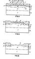
- the mask is formed by depositing a blanked layer 14 (see Fig. 2) of photoresist and then exposing and developing the layer 14 of photoresist to produce portions of the layer 14 of photoressit as shown in Fig. 2.
- the remaining portions of the layer 14 of photoresist function as a mask to enable etching of openings 15 (see Fig. 2) in the layer 12 of silicon dioxide.
- This etching of the layer 12 of silicon dioxide to form the openings 15 therein may be by buffered hydrofluoric acid solution, which may be a 7:1 solution, for example, or by reactive ion etching (RIE) using a gas of CF 4 -H 2 , for example.
- buffered hydrofluoric acid solution which may be a 7:1 solution, for example, or by reactive ion etching (RIE) using a gas of CF 4 -H 2 , for example.
- RIE reactive ion etching
- N+ region 16 is then formed in the epitaxial layer 11 through each of the openings 15 in the layer 12 of silicon dioxide.
- the N+ region 16 is formed by diffusion or ion implantation.
- the diffused impurity may be phosphorous or arsenic.
- N+ region 16 in the epitaxial layer 11 is by ion implantation of arsenic ions having a concentration or dose of about 5 x 10 15 atoms/cm and at an energy of 70 keV.
- arsenic ions having a concentration or dose of about 5 x 10 15 atoms/cm and at an energy of 70 keV.
- a plurality of the N+ regions 16 is formed in the epitaxial layer 11 at desired locations in accordance with the openings 15 in the layer 12 of silicon dioxide.
- the remaining portions of the layer 14 of photoresist are stripped by a solvent and an acid or oxygen plasma and an acid, for example. Then, a very thin layer 17 (see Fig. 3) of silicon dioxide is formed over each of the N+ regions 16.
- the layer 17 of silicon dioxide is preferably formed by thermal oxidation with the same conditions as the layer 12 of silicon dioxide was thermally grown.
- the layer 17 of silicon dioxide has a thickness of 40 nm.
- a layer 18 of silicon nitride is deposited over the layer 17 of silicon dioxide and the layer 12 of silicon dioxide.
- the layer 18 of silicon nitride is preferably deposited as a conformal coating by low pressure chemical vapor deposition (LPCVD) and preferably has a thickness of 100 nm.
- a mask is placed over the layer 18 of silicon nitride.
- the mask is formed by depositing a blanket layer 19 (see Fig. 4) of photoresist and then exposing and developing the layer 19 of photoresist to produce portions of the layer 19 of photoresist as shown in Fig. 4.
- the remaining portions of the layer 19 of photoresist function as the mask to enable etching of the layer 18 of silicon nitride to remove portions of the layer 18 of silicon nitride not protected by the remaining portions 19 of photoresist.
- This etching of the layer 1 8 of silicon nitride may be by a plasma gas of CF 4 -0 2 or RIE with a gas of CF 4 -H 2 , for example.
- the remaining portions of the layer 19 of photoresist are stripped by a solvent and an acid or oxygen plasma and an acid, for example.
- the remaining portions of the layer 18 of silicon nitride overlie most but not all of each of the N+ regions 16.
- boron ions there is an ion implantation of boron ions into the epitaxial layer 11 in all of the areas not having one of the N+ regions 16. These implanted boron ions form a channel stopper, which is a P+ region 20, in the epitaxial layer 11.
- One suitable example of implanting boron ions is to implant boron ions having a concentration of 6 x 1 0 12 atoms/cm 2 and at an energy of 80 keV.
- the boron ion implantation can occur before or after etching of the layer 18 of silicon nitride.
- the boron ion implantation occurs after etching of the layer 18 of silicon nitride, it can occur before or after stripping of the layer 19 of photoresist.
- the remaining portions of the layer 19 of photoresist are stripped before the ion implantation, there is re- oxidation over each of the N+ regions 16 in the areas not protected by the remaining portions of the layer 18 of silicon nitride if the exposed portions of the layer 17 of silicon dioxide do not have a thickness of at least 20 nm.
- the ions are implanted through the layer 17 of silicon dioxide or the newly grown thin layer of silicon dioxide having a thickness of at least 20 nm with a blanket implantation. It is preferred that ion implantation occur after etching of the layer 18 of silicon nitride and before removal of the remaining portions of the layer 19 of photoresist.
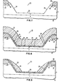
- recessed isolation oxide (ROX) regions 22 are formed by thermal oxidation, preferably in the presence of steam at a temperature of about 925 °C.
- the ROX regions 22 have a thickness of about 400 nm to 600 nm. This results in spaced portions of each of the N + regions 16 being surrounded by the ROX regions 22 because of the presence of the layer 18 of silicon nitride over most but all of each spaced portion of each of the N+ regions 16.
- each of the N+ regions 16 changes, as shown in Fig. 5, during formation of the ROX regions 22 because of the impurities of the dopant, which forms the N+ regions 16, moving downwardly into the epitaxial layer 11.
- the cross section of each of the N+ regions 16 is slightly bent at its periphery by the thermal growth of the ROX regions 22, it is still disposed in the (100) plane.
- the remaining portions of the layer 18 of silicon nitride are removed.
- the remaining portions of the layer 18 of silicon nitride are preferably removed by etching in a hot phosphoric acid (H 3 P0 4 ) for ninety minutes at a temperature of about 165 °C, for example.
- the substrate 10 is dip etched in a buffered hydrofluoric acid solution, which may be 7:1 solution, for example, to remove the very thin layer 17 of silicon dioxide over each of the N+ regions 16. This produces the structure shown in Fig. 6.
- a buffered hydrofluoric acid solution which may be 7:1 solution, for example, to remove the very thin layer 17 of silicon dioxide over each of the N+ regions 16.
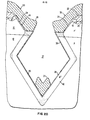
- a recess 23 (see Fig. 7) is formed through each of the spaced portions of the N+ regions 16 and into the epitaxial layer 11.
- the recess 23 has its side walls 24 (two shown in Fig. 7) converging from its upper end at the top surface of the N+ region 16 to a bottom wall 25, which is along a (100) plane.
- the side walls 24 of the recess 23 form a substantially V-shaped relation through being along the (111) plane in the epitaxial layer.11.
- This directional etching of each of the spaced portions of each of the N+ regions 16 and the underlying epitaxial layer 11 is produced by etching with a suitable anisotropic etchant, which is an etchant that etches in a direction along the (111) planes and is preferably a pyrocathecol-ethylenediamine solution.
- a suitable anisotropic etchant which is an etchant that etches in a direction along the (111) planes and is preferably a pyrocathecol-ethylenediamine solution.
- the concentration of the epitaxial layer 11 increases towards the interface of the epitaxial layer 11 with the substrate 10, this increased concentration of the dopant cuases the etch rate to decrease.
- etching may be easily stopped with the bottom wall 25 of the recess 23 within the epitaxial layer 11.
- the conductivity of the epitaxial layer 11 is P- because the substrate 10 has a P conductivity, the etching must be more closely monitored to stop etching at the desired time so that there is no penetration of the recess 23 into the substrate 10.
- each of the recesses 23 is surrounded by the spaced portion of the N+ regions 16 through which it is formed.
- the upper end of each of the side walls 24 of the recess 23 terminates at the top surface of the spaced portion of the N+ region 16.
- the protective layer of material includes a layer 26 (see Fig. 8) of silicon dioxide, which is formed on the bottom wall 25 of the recess 23, the side walls 24 of the recess 23, andthe portions of the top surface of the spaced portions of the N+ region 16 not covered by the ROX regions 22.
- the layer 26 of silicon dioxide is preferably thermally grown.
- the thickness of portions 27 of the layer 26 of silicon dioxide along the side walls 24 of each of the recesses 23 below the spaced portion of the N+ region 16 is about 1.2 times the thickness of portion 28 of the layer 26 of silicon dioxide along the bottom wall 25 of each of the recesses 23.
- the thickness of portion 29 of the layer 26 of silicon dioxide on each of the side walls 24 along the spaced portion of the N+ region 16 is in a range of 1.4 to 2 times the thickness of the portion 28 of the layer 26 of silicon dioxide over the bottom wall 25 of each of the recesses 23.
- the thickness of the portion 27 along each of the side walls 24 beneath each of the spaced portions of each of the N+ regions 16 would be 50 nm while the thickness of the portion 29 along each of the side walls 24 opposite each of the spaced portions of each of the N+ regions 16 would be in a range of 56 nm to 80 nm.
- the temperature at which the thermal oxidation occurs is selected to maximize this relationship of the thickness of various portions of thel layer 26 of silicon dioxide. As the temperature increases, the thicknesses of the portions 27-29 of the layer 26 of silicon dioxide would tend to become more equal. Accordingly, when thermally growing the layer 26 of silicon dioxide in steam, the temperature is in the range of 800 °C to 925 °C.
- a layer 30 of silicon nitride is deposited as a conformal coating by LPCVD in the same manner as the layer 18 of silicon nitride was deposited.
- the thickness of the layer 30 os silicon nitride is preferably 100 nm.
- a layer 31 of silicon dioxide is deposited over the layer 30 of silicon nitride.
- the layer 31 of silicon dioxide if preferably deposited by LPCVD with a thickness of one micron.
- the layer 31 of silicon dioxide is subjected to RIE by a suitable gas such as CF 4 -H 2 , for example. This removes the layer 31 of silicon dioxide except for a portion 32 of silicon as shown in Fig. 9.
- the portion 32 of silicon dioxide functions as a mask during RIE of the layer 30 of silicon nitride.
- RIE of the layer 30 of silicon nitride will leave a portion 33 of silicon nitride beneath the portion 32 of silicon dioxide as shown in Fig. 10.
- Suitable gases for RIE of the layer 30 (see Fig. 8) of silicon nitride include CF 4 -0 2 , CCl 2 -F 2 , and S F 6 -C1 2 .
- the layer 26 of silicon dioxide is subjected to RIE with the same gas as was used in RIE of the layer 31 (see Fig. 8) of silicon dioxide.
- RIE reactive ion etching
- the remaining portion of the layer 26 of silicon dioxide, the portion 33 of silicon nitride, and the portion 32 of silicon dioxide form a protective layer of material over the side walls 24 of each of the recesses 23.
- This protective layer of material extends above the top surface of the N+ region 16.
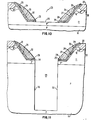
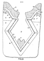
- a trench or recess 35 (see Fig. 11) is formed through each of the openings 34 through the epitaxial layer 11 and into the substrate 10 for a selected distance.
- the opening 34 in each of the bottom portions 28 of the layer 26 of silicon dioxide is square with each side being 2 um, the maximum depth of the trench or recess 35 is 8.7 um.
- the trench or recess 35 if preferably formed by RIE. Any of the gases employed in RIE of the layer 30 (see Fig. 9) of silicon nitride may be employed to form the trench or recess 35 (see Fig. 11).
- trench or recess 35 is preferably formed by R IE , it should be understood that the trench or recess 35 could be formed with a suitable plasma and would have side walls 36 (two shown in Fig. 11) substantially vertical. This is a sirectional plasma capable of etching substantially vertical side walls.
- the side walls 36 which are in the (110) plane, of the trench or recess 35 are subjected to chemical etching by an anisotropic etchant in the same manner and with the same etchant as used to form each of the recesses 23 (see Fig. 7).
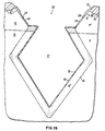
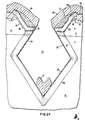
- the opening 34 (see Fig. 11) in each of the bottom portions 28 of the layer 26 of silicon idoxide is square so that the top of the recess 37 is square as shown in Fig. 16, the converging side walls 38 engage each other at their bottoms as shown in Fig. 17.
- the opening 34 (see Fig. 11) in each of the bottom portions 28 of the layer 26 of silicon dioxide is rectangular with one of the sides being 2 ⁇ m and the other 3.8 jam, for example, so that the top of the recess 37 is rectangular as shown in Fig. 13, then the recess 37 has the configuration shown in Fig. 14 in one direction and the configuration of Fig. 15 orthogonal thereto. In the direction of Fig.
- each of the recesses 37 may be deemed to be formed of a portion of each of two (upper and lower) four-sided pyramids.
- an N+ region 40 (see Fig. 19) is formed exterior of the side walls 38 of each of the recesses 37 by a suitable diffusion.
- One means of diffusing an impurity into the side walls 38 of each of the recesses 37 to form each of the N+ regions 40 is to deposit a layer 41 (see Fig. 18) of phosphosilicate glass.
- the layer 41 of phosphosilicate glass is grown by passing POCl 3 and oxygen over the entire substrate 10 in a furnace at a temperature of 870 °C.
- the phosphorous from the layer 41 of phosphosilicate glass is driven into the portions of the epitaxial layer 11 and the substrate 10 in contact with the layer 41 of phosphosilicate glass and not protected by either silicon nitride or silicon dioxide.
- the phosphorous is driven out of the layer 41 of phosphosilicate glass at a temperature of 925 C for fifteen to thirty minutes to produce each of the N+ regions 40 (see Fig. 19).
- the length of time is determined by the desired thickness of each of the N+ regions 40 with the thickness preferably being about 0.25 nm.
- the layer 41 (see Fig. 18) of phosphosilicate glass is stripped through dip etching with a buffered hydrofluoric acid solution, which may be a 7:1 solution, for example.
- the buffered hydrofluoric acid solution etches the layer 41 of phosphosilicate glass faster than it etches silicon dioxide.
- this dip etch also etches the portion 32 of silicon dioxide on top of the portion 33 of silicon nitride in each of the recesses 23.
- the portion 33 of silicon nitride in each of the recesses 23 is removed by wet etching. This is accomplished by etching the portion 33 of silicon nitride in a hot phoshoric acid at a temperature of 165 °C, for example.
- the remaining portions of the layer 26 of silicon dioxide are removed.
- the remaining portions of the layer 26 of silicon dioxide are removed by a wet etch in a buffered hydrofluoric acid solution, which may be a 7:1 solution, for example.
- a layer 43 (see Fig. 19) of silicon dioxide is formed over the N+ region 40 and the side walls 24 of each of the recesses 23 including the end of the spaced portions of the N+ region 16.
- the layer 43 of silicon dioxide has a thickness in the range of 22.5 nm to 80 nm depending on the desired threshold voltage of the gate voltage.
- the layer 43 of silicon dioxide is preferably thermally grown.
- the layer 43 of silicon dioxide may be grown in steam at a temperature of 800 C or dry oxygen at 925 °C.
- the layer 43 of silicon dioxide has its portion 44 over the side walls 24 of each of the recesses 23 functioning as a gate oxide since a portion of the epitaxial layer 11 between the spaced portion of the N + region 16 and the upper end of the N+ region 4 0 is a gate channel. Therefore, the spaced portion of the N + region 16 is a drain region while the N+ region 40 is a source region as well as a plate of a capacitor with the substrate 10 being the other plate of the capacitor.
- a mask is placed over the layer 43 of silicon dioxide.
- the mask is formed by depositing a blanket layer of photoresist and then exposing and developing the layer of photoresist to produce openings in the layer of photoresist.
- the remaining portions of the layer of photoresist function as a mask to enable etching of contact holes 47 (see Fig. 22) in the ROX regions 22 through the openings in the layer of photoresist.
- This etching may be either by a buffered hydrofluoric acid solution, which may be a 7:1 solution, for example, or RIE with CF 4 -H 2 gas, for example.
- each of the N+ regions 16 which are separated from each other by the channel stoppers 20. This is because each of the N+ regions 16, which function as bit lines and extend in one direction substantially parallel to each other, will have only a single contact with a conductive line 48 (see Fig. 21).
- the remaining portions of the layer of photoresist are stripped by a solvent and an acid or oxygen plasma and an acid, for example.
- a suitable conductive material such as aluminium, tungsten silicide, or polycrystalline silicide, for example, is deposited as a blanket coating over the substrate 10.
- a layer 49 (see Fig. 20) of aluminium is deposited as a blanket coating over the substrate 10.
- the layer 49 of aluminium extends through the contact hole 47 (see Fig. 22) to have electrical contact with the N+ region 16 exterior of the storage cells as shown in Fig. 21.
- each of the word lines has an electrical contact with the gate channel of each of the FETs in a row extending orthogonal to a row of the FETs having the N+ region 16 connected to one of the conductive lines 48.
- the layer 49 (see Fig. 20) of aluminum may be etched by any well-known method.
- the layer 49 of aluminum may be etched by subtractive etching or using a lift-off mask.
- subtractive etching a mask, which may be formed by the well-known photoresist technique, is placed over the layer 39 of aluminum. Then, a suitable etchant is employed to etch the aluminum through the openings in the mask to form the conductive lines 48 (see Fig. 21) and the word lines 50.
- a mask is put down before the layer 49 (see Fig. 20) of aluminum is deposited.
- the mask may be formed by the well-known photoresist technique with openings being formed in the mask wherever the conductive lines 48 (see Fig. 21) or the word lines 50 are to be formed. Then, the mask is lifted off with the portions of the layer 49 (see Fig. 20) of aluminum that are to be removed.
- a layer 52 of polycrystalline silicon is beneath the layer 49 of aluminum so that portions of the layer 52 of polycrystalline silicon function along with portions of the layer 49 of aluminum as the conductive lines 48 (see Fig. 21) and the word lines 50.
- the layer 52 (see Figs. 23 and 24) of polycrystalline silicon is deposited by LPCVD after the contact holes 47 (see Fig. 22) have been formed in the ROX regions 22. All of the prior formation steps of this embodiment are the same as described with respect to Figs. 1-22.
- the thickness of the layer 52 (see Figs. 23 and 24) of polycrystalline silicon is in the range of 200 nm to 300 nm and preferably is 250 nm.
- the layer 52 of polycrystalline silicon is deposited, it is then doped by any suitable means to have the desired conductivity.
- the substrate 10 may be placed in a furnace at 870 °C for twenty-five minutes. During the first ten minutes, only N 2 gas is used. For the next ten minutes, a gaseous mixture of N 2 -0 2 -POC1 3 is passed through the furnace. Finally, only 0 2 gas flows through the furnace for five minutes. This produces a layer of phosphosilicate glass, which must then be stripped.
- stripping the layer of phosphosilicate glass is through dip etching with a buffered hydrofluoric acid solution, which may be a 10:1 solution, for example. This solution etches the layer of phosphosilicate glass at a much faster rate than silicon.
- a buffered hydrofluoric acid solution which may be a 10:1 solution, for example. This solution etches the layer of phosphosilicate glass at a much faster rate than silicon.
- the dopant is driven into the layer 52 of polycrystalline silicon by subjecting the substrate 10 to a temperature of 1,000 C for fifteen minutes in an argon gas. This produces the desired level of doping of the layer 52 of polycrystalline silicon.
- the layer 52 of polycrystalline silicon is doped to have a sheet resistivity in the range of 25-40 ohms/square and preferably about 32 ohms/square.
- the layer 49 of aluminum is deposited as a blanket coating in the same manner as discussed with respect to Fig. 20.
- the layer 49 of aluminum is then etched in the manner previously described for forming the conductive lines 48 (see Fig. 21) and the word lines 50.
- the substrate 10 is annealed to cause the aluminum, which forms the conductive lines 48 and the word lines 50, to make good electrical contact to the portions of the layer 52 (see Figs. 23 and 24) of polycrystalline silicon therebeneath.
- This annealing occurs at a temperature of 400 °C for thirty minutes in a forming gas of 95 % nitrogen and 5 % hydrogen.
- the layer 52 of polycrystalline silicon is etched by a pyrocathecol-ethylenediamine solution. This results in the remaining portions of the layer 52 of polycrystalline silicon being beneath the remaining portions of the layer 49 of aluminum so that they cooperate together to form the conductive lines 48 (see Fig. 21) and the word lines 50.
- the deposition of the layer 49 (see Fig. 23) of aluminum causes the portion 51 of aluminum to fall to the bottom of the recess 37.
- the portion 51 of aluminum rests on a portion 53 (see Fig. 24) of polycrystalline silicon after the layer 52 of polycrystalline silicon is etched.
- the portion 53 of polycrystalline silicon remains after etching because the portion 51 of aluminum functions as a mask during etching.
- the portion of the layer 52 (see Fig. 23) of polycrystalline silicon within each of the recesses 37 may be etched by a pyrocathecol-ethylenediamine solution prior to any etching of the layer 49 of aluminum. This avoids any difficulty in exposing the layer of photoresist, which is used to etch the layer 49 of aluminum, within each of the recesses 37 as all of the photoresist must be removed to etch the portion of the layer 52 of polycrystalline silicon in each of the recesses 37.
- a layer of aluminum is deposited as a blanket coating. This cannot be deposited in each of the recesses 37 other than at the bottom of each of the recesses 37 as occurs with the portion 51 of aluminum when the layer 49 of aluminum is deposited. Then, the layer 52 of polycrystalline silicon in each of the recesses 37 is etched with the layer of aluminum functioning as a mask for the portions of the layer 52 of polycrystalline silicon not in one of the recesses 37. After etching of the layer 52 of polycrystalline silicon, the mask layer of aluminum is completely stripped.
- a mask is put down by the well-known photoresist technique with openings being formed in the mask wherever the conductive lines 48 (see FIG. 21) and the word lines 50 are to be formed.
- the layer 49 (see FIG. 23) of aluminum is deposited. Then, the mask is lifted off with the portions of the layer 49 of aluminum that are to be removed.
- the layer 52 (see FIG. 23) of polycrystalline silicon is etched to form parts of the conductive lines 48 (see FIG. 21) and the word lines 50. Then, the substrata 10 is annealed in the same manner as previously described after etching of the layer 52 (see FIG. 23) of polycrystalline silicon is completed.
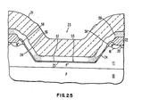
- FIG. 25 there is shown a stage of formation of the dense vertical FET replacing the stage of formation shown in FIG. 8.
- a layer 55 of silicon dioxide is formed over the bottom wall 25 of the recess 23, the side walls 24 of the recess 23, and the portions of the top surface of the spaced portion of the N+ region 16 not covered by the ROX regions 22.
- the layer 55 of silicon dioxide is preferably thermally grown.
- the thickness of portions 56 of the layer 55 of silicon dioxide along the side walls 24 of each of the recesses 23 below the spaced portion of the N+ region 16 is about 1.2 times the thickness of portion 57 of the layer 55 of silicon dioxide along the bottom wall 25 of each of the recesses 23.
- the thickness of portions 58 of the layer 55 of silicon dioxide on each of the side walls 24 along the spaced portion of the N+ region 16 is in a range of 1.4 to 2 times the thickness of the portion 57 of the layer 55 of silicon dioxide over the bottom wall 25 of each of the recesses 23.
- the thickness of the portion 56 of the layer 55 of silicon dioxide is preferably in the range of 22.5 nm to 50 nm.
- the temperature at which the thermal oxidation occurs is selected to maximize this relationship of the thicknesses of various portions of the layer 55 of silicon dioxide. As the temperature increases, the thicknesses of the portions 56-58 of the layer 55 of silicon dioxide would tend to become more equal. Accordingly, when thermally growing the layer 55 of silicon dioxide in steam, the temperature is in the range of 800° C. to 925° C.
- a layer 59 of polycrystalline silicon is deposited by LPCVD as a blanket coating.
- the layer 59 of polycrystalline silicon must be doped at the time of deposition or it may be doped after deposition in the manner previously described for doping the layer 52 (see FIG. 23) of polycrystalline silicon.
- the layer 59 of polycrystalline silicon has the same sheet resistivity as the layer 52 of polycrystalline silicon.
- the layer 31 of silicon dioxide is deposited in the same manner as previously described with respect to FIG. 8.
- the layer 31 of silicon dioxide is preferably deposited by LPCVD with a thickness of 1 pm.
- FIG. 25 is subjected to the same steps of formation as shown and described with respect to FIGS. 9-18.
- the layer 41 (see FIG. 18) of phosphosilicate glass is grown, the N+ region 40 is formed in the same manner as described with respect to FIG. 19.
- the layer 41 (see FIG. 18) of phosphosilicate glass is stripped. As described with respect to FIG. 19, this stripping of the layer 41 (see FIG. 18) of phosphosilicate glass also etches the portion 32 of the layer 31 of silicon dioxide.
- tne layer 59 (see FIG. 25) of polycrystalline silicon protecting the layer 55 of silicon dioxide
- the necessity for removing the portion 56 of the layer 55 of silicon dioxide over the side walls 24 of each of the recesses 23 and the remaining portions 57 of the layer 55 of silicon dioxide is eliminated so that the layer 55 of silicon dioxide can function as the gate oxide.
- the layer 55 of silicon dioxide does not have unbonded surface states thereon as occur when protecting the layer 26 (see FIG. 8) of silicon dioxide with the layer 30 of silicon nitride. Therefore, it is not necessary to either remove the layer 55 (see FIG. 25) of silicon dioxide or have the additional step of adding the layer 43 of silicon dioxide to serve as a gate oxide as described with respect to FIG. 19.
- the conductive lines 48 see FIG. 21
- the word lines 50 through depositing the layer 49 (see FIG. 20) of aluminum as a blanket coating as described with respect to FIG. 20.
- the layer 49 of aluminum is etched to produce the conductive lines 48 (see FIG. 21) and the word lines 50. This may be accomplished in the manner described with respect to the stages of formation shown in FIGS. 23 and 24. This produces the structure shown in FIG. 26.
- the layer 59 of polycrystalline silicon is removed from the upper surface of the substrate 10 during etching to form the recesses 37. Therefore, the conductive lines 48 (see FIG. 21) would not include any of the layer 59 of polycrystalline silicon as the layer 52 of polycrystalline silicon was included in the embodiment disclosed in FIGS. 23 and 24.
- the word lines 50 include both the remaining portions of the layer 59 of polycrystalline silicon over the portion 56 of silicon dioxide functioning as the gate oxide and the etched portions of the layer 49 of aluminum as shown in FIG. 26.
- the layer 59 of polycrystalline silicon may be etched to form the word lines 50 before the layer 31 of silicon dioxide is deposited.
- the well-known photoresist technique could be employed to produce a mask of photoresist over the portions of the layer 59 of polycrystalline silicon that are to be part of the word lines 50. Then, the layer 31 of silicon dioxide would be deposited in the manner previously described.
- the layer 41 (see FIG. 18) of phosphosilicate glass is not stripped so that the portion 32 of the layer 31 of silicon dioxide also is not etched since there is no stripping of the layer 41 of phosphosilicate glass.
- the portion 56 of the layer 55 of silicon dioxide functions as the gate oxide.
- the N+ region 40 (see FIG. 19) has been produced, it is only necessary to form the conductive lines 48 (see FIG. 20) and the metal portions of the word lines 50 through depositing the layer 49 of aluminum as a blanket coating as described with respect to FIG. 20.
- the layer 49 of aluminum is etched to produce the conductive lines 48 and the metal portions of the word lines 50. This may be accomplished in the manner described with respect to the stages of formation shown in FIGS. 23 and 24. This produces the structure shown in FIG..27.
- conductive lines 48 and the word lines 50 have been shown and described as including at least aluminum, it should be understood that any other suitable conductive material may be employed. This could include metal silicides, for example.
- the substrate 10 has been described as having the epitaxial layer 11, it should be understood that the epitaxial layer 11 is optional. Therefore, the present invention does not require the epitaxial layer 11 although it is preferred.
- An advantage of this invention is that it does not require a buried storage node to have increased density as in a VMOS memory cell. Another advantage of this invention is that it eliminates the point break down problem of the VMOS memory cell. A further advantage of this invention is that it does not require outdiffusion for control of. the threshold voltage of the FET device. Still another advantage of this invention is that it has an increased charge transfer efficiency in comparison with VMOS memory cells when it has a comparable density with the VMOS memory cells.
Abstract
Description
- This invention relates to a dense vertical field effect transistor (FET) and a method for making and, more particularly, to a high density memory cell of an FET and a method of making.
- In US patent 4 105 475 to Jenne, there is shown a semiconductor device having an array of single transistor VMOS memory cells. Each of the cells includes a storage capacitor region in a substrate with a V-shaped recess extending thereinto and having the oxide of a gate element on its walls. A drain region of each of the memory cells is in surrounding relation to the V-shaped recess and closer to the upper end of the channel region of the gate element than the lower end.
- One problem with the VMOS memory cell of the aforesaid Jenne patent is that it requires a buried storage capacitor if the semiconductor device is to have a relatively high density of the VMOS memory cells thereon. However, this requires an additional processing step.
- Another problem with the VMOS memory cell of the aforesaid Jenne patent is that the gate oxide has a tendency to break down at the bottom of the V-shaped recess when subjected to a relatively low voltage. This point breakdown of the gate oxide causes the storage cell to cease to function properly.
- A further problem with the VMOS memory cell of the aforesaid Jenne patent is that it depends upon an outdiffusion during growth of an epitaxial layer to control the threshold voltage between the gate channel region and the substrate. Thus, it is a requisite of the VMOS memory cell of the aforesaid Jenne patent that the substrate include an epitaxial layer.
- The present invention as claimed overcomes the foregoing problems in that there is no requirement for any buried storage capacitor in a dense vertical FET device used as a high density memory cell. There also is no point formed for the gate oxide so that the point breakdown of the gate oxide is eliminated. The present invention also does not require the growth of an epitaxial layer to control the threshold voltage since it utilizes an ion implantation to control the threshold voltage. It is not possible to implant ions in a VMOS memory cell at the time that such is required to control the threshold voltage.
- Additionally, the present invention also has a substantially higher density of memory cells in comparison with the density of the VMOS memory cells.
- One means of increasing the charge storage region of a memory cell is through forming an enlarged wall in the substrate.
- The present invention is also an improvement of the prior art in that only one of the drain and source regions is formed in the surface of the substrate. Thus, the density of the memory cells of the present invention can be increased beyond the memory cell density of the prior art structure.
- The dense vertical FET device of the present invention reduces the area required for each device through having only one of the drain and source regions of the FET formed in the surface of the substrate. The other of the source and drain regions of the FET is formed in the substrate beneath the one region of the FET in the surface of the substrate. Thus, a relatively small surface area on the substrate is required for each of the FETs.
- The foregoing and other objects, features, and advantages of the invention will be more apparent from the following more particular description of the preferred embodiments of the invention as illustrated in the accompanying drawings.
-
- Figs. 1-12 are fragementary diagrammatic sectional views of a portion of a substrate showing various stages of formation of a dense vertical FET device in the substrate.
- Fig. 13 is a fragmentary perspective view of a portion of the substrate showing a stage in forming the dense vertical FET device and taken along line 13-13 of Fig. 12.
- Fig. 14 is a fragmentary sectional view of the portion of the substrate of Fig. 13 and taken along line 14-14 of Fig. 13.
- Fig. 15 is a fragmentary sectional view of the portion of the substrate of Fig. 13 and taken along line 15-15 of Fig. 13.
- Fig. 16 is a fragmentary perspective view of a portion of the substrate showing a stage in forming the dense vertical FET device and taken along line 13-13 of Fig. 12.
- Fig. 17 is a fragmentary sectional view of the portion of the substrate of Fig. 16 and taken along line 17-17 of Fig. 16.
- Figs. 18 & 19 are fragmentary diagrammatic sectional views of a portion of the substrate showing further stages of formation of the dense vertical FET device in the substrate.
- Fig. '2Q is a fragmentary diagrammatic sectional view of a portion of ths substrate showing another stage of formation of the dense vertical FET device and taken along line 20-20 of Fig. 21.
- Fig. 21 is a fragmentary top plan view of a portion of a substrate in which dense vertical FET devices are formed and at the stage of formation shown in Fig. 20.
- Fig. 22 is a fragmentary diagrammatic sectional view of a portion of the substrate showing the same stage of formation of the dense vertical FET device as Fig. 20 and taken along line 22-22 of Fig. 21.
- Figs. 23 & 24 are fragmentary diagrammatic sectional views of a portion of the substrate showing various stages of formation of a modification of the dense vertical FET device.
- Figs. 25 & 26 are fragmentary diagrammatic sectional views of a portion of the substrate showing various stages of formation of another modification of the dense vertical FET device.
- Fig. 27 is a fragmentary diagrammatic sectional view of a portion of the substrate showing a stage of formation of a further modification of the dense vertical FET device.
- Referring to the drawings and particularly Fig. 1, there is shown a
substrate 10 of monocrystalline silicon having a <100> orientation. Thesubstrate 10 may be either P or P+ conductivity with thesubstrate 10 perferably being of P conductivity. - An
epitaxial layer 11 is grown form thesubstrate 10 by any conventional techniques. Theepitaxial layer 11 has a P conductivity when thesubstrate 10 has a P+ conductivity and has a P- conductivity when thesubstrate 10 has a P conductivity. - One suitable example of growing the
epitaxial layer 11 is to use a mixture of SiCl4-H2 or SiH4-H2 at a temperature of about 1000 °C, for example. Theepitaxial layer 11 may have a thickness in the range of 2 to 6 µm and preferably has a thickness in the range of 3 to 4 µm. Theepitaxial layer 11 has a maximum impurity concentration or doping level of about 1015 atoms/cm3. - After the
epitaxial layer 11 has been grown, alayer 12 of silicon dioxide is formed on top of theepitaxial layer 11. Thelayer 12 of silicon dioxide may be formed through oxidizing a portion of theepitaxial layer 11, for example. When thelayer 12 of silicon dioxide is formed through oxidizing a portion of theepitaxial layer 11, a portion of theepitaxial layer 11 must remain so that it still has a thickness of at least 70 nm to 200 nm after oxidation. - This thermal oxidation may occur in either dry oxygen or steam at a temperature in the range of 800 °C to 1050 o C, for example. When using steam, a temperature of 925 °C is preferred.
- Instead of growing the
layer 12 of silicon dioxide on theepitaxial layer 11, thelayer 12 of silicon dioxide may be deposited by chemical vapor deposition (CVD). The thickness of thelayer 12 of silicon dioxide is in the range of 100 nm to 500 nm and is preferably about 200 nm. - After the
layer 12 of silicon dioxide is formed, a mask is placed over thelayer 12 of silicon dioxide. The mask is formed by depositing a blanked layer 14 (see Fig. 2) of photoresist and then exposing and developing thelayer 14 of photoresist to produce portions of thelayer 14 of photoressit as shown in Fig. 2. - The remaining portions of the
layer 14 of photoresist function as a mask to enable etching of openings 15 (see Fig. 2) in thelayer 12 of silicon dioxide. This etching of thelayer 12 of silicon dioxide to form theopenings 15 therein may be by buffered hydrofluoric acid solution, which may be a 7:1 solution, for example, or by reactive ion etching (RIE) using a gas of CF4-H2, for example. - An
N+ region 16 is then formed in theepitaxial layer 11 through each of theopenings 15 in thelayer 12 of silicon dioxide. TheN+ region 16 is formed by diffusion or ion implantation. The diffused impurity may be phosphorous or arsenic. - One suitable example of forming the
N+ region 16 in theepitaxial layer 11 is by ion implantation of arsenic ions having a concentration or dose of about 5 x 10 15 atoms/cm and at an energy of 70 keV. Thus, a plurality of theN+ regions 16 is formed in theepitaxial layer 11 at desired locations in accordance with theopenings 15 in thelayer 12 of silicon dioxide. - After the
N+ regions 16 have been formed in theepitaxial layer 11 of thesubstrate 10, the remaining portions of thelayer 14 of photoresist are stripped by a solvent and an acid or oxygen plasma and an acid, for example. Then, a very thin layer 17 (see Fig. 3) of silicon dioxide is formed over each of theN+ regions 16. Thelayer 17 of silicon dioxide is preferably formed by thermal oxidation with the same conditions as thelayer 12 of silicon dioxide was thermally grown. Thelayer 17 of silicon dioxide has a thickness of 40 nm. - After the
layer 17 of silicon dioxide is formed over each of theN+ regions 16, alayer 18 of silicon nitride is deposited over thelayer 17 of silicon dioxide and thelayer 12 of silicon dioxide. Thelayer 18 of silicon nitride is preferably deposited as a conformal coating by low pressure chemical vapor deposition (LPCVD) and preferably has a thickness of 100 nm. - After the
layer 18 of silicon nitride is deposited, a mask is placed over thelayer 18 of silicon nitride. The mask is formed by depositing a blanket layer 19 (see Fig. 4) of photoresist and then exposing and developing thelayer 19 of photoresist to produce portions of thelayer 19 of photoresist as shown in Fig. 4. - The remaining portions of the
layer 19 of photoresist function as the mask to enable etching of thelayer 18 of silicon nitride to remove portions of thelayer 18 of silicon nitride not protected by the remainingportions 19 of photoresist. This etching of the layer 18 of silicon nitride may be by a plasma gas of CF4-02 or RIE with a gas of CF4-H2, for example. - After the
layer 18 of silicon nitride has been etched to leave only the portions of thelayer 18 of silicon nitride beneath the remaining portions of thelayer 19 of photoresist, the remaining portions of thelayer 19 of photoresist are stripped by a solvent and an acid or oxygen plasma and an acid, for example. Thus, the remaining portions of thelayer 18 of silicon nitride overlie most but not all of each of theN+ regions 16. - There is an ion implantation of boron ions into the
epitaxial layer 11 in all of the areas not having one of theN+ regions 16. These implanted boron ions form a channel stopper, which is aP+ region 20, in theepitaxial layer 11. One suitable example of implanting boron ions is to implant boron ions having a concentration of 6 x 10 12 atoms/cm 2 and at an energy of 80 keV. - The boron ion implantation can occur before or after etching of the
layer 18 of silicon nitride. When the boron ion implantation occurs after etching of thelayer 18 of silicon nitride, it can occur before or after stripping of thelayer 19 of photoresist. When the remaining portions of thelayer 19 of photoresist are stripped before the ion implantation, there is re- oxidation over each of theN+ regions 16 in the areas not protected by the remaining portions of thelayer 18 of silicon nitride if the exposed portions of thelayer 17 of silicon dioxide do not have a thickness of at least 20 nm. Then, the ions are implanted through thelayer 17 of silicon dioxide or the newly grown thin layer of silicon dioxide having a thickness of at least 20 nm with a blanket implantation. It is preferred that ion implantation occur after etching of thelayer 18 of silicon nitride and before removal of the remaining portions of thelayer 19 of photoresist. - Next, recessed isolation oxide (ROX) regions 22 (see Fig. 5) are formed by thermal oxidation, preferably in the presence of steam at a temperature of about 925 °C. The
ROX regions 22 have a thickness of about 400 nm to 600 nm. This results in spaced portions of each of the N+regions 16 being surrounded by theROX regions 22 because of the presence of thelayer 18 of silicon nitride over most but all of each spaced portion of each of theN+ regions 16. - The cross sectional shape of each of the
N+ regions 16 changes, as shown in Fig. 5, during formation of theROX regions 22 because of the impurities of the dopant, which forms theN+ regions 16, moving downwardly into theepitaxial layer 11. Although the cross section of each of theN+ regions 16 is slightly bent at its periphery by the thermal growth of theROX regions 22, it is still disposed in the (100) plane. - After the
ROX regions 22 have been formed, the remaining portions of thelayer 18 of silicon nitride are removed. The remaining portions of thelayer 18 of silicon nitride are preferably removed by etching in a hot phosphoric acid (H3P04) for ninety minutes at a temperature of about 165 °C, for example. - Then the
substrate 10 is dip etched in a buffered hydrofluoric acid solution, which may be 7:1 solution, for example, to remove the verythin layer 17 of silicon dioxide over each of theN+ regions 16. This produces the structure shown in Fig. 6. - Next, a recess 23 (see Fig. 7) is formed through each of the spaced portions of the
N+ regions 16 and into theepitaxial layer 11. Therecess 23 has its side walls 24 (two shown in Fig. 7) converging from its upper end at the top surface of theN+ region 16 to abottom wall 25, which is along a (100) plane. Theside walls 24 of therecess 23 form a substantially V-shaped relation through being along the (111) plane in the epitaxial layer.11. - This directional etching of each of the spaced portions of each of the
N+ regions 16 and theunderlying epitaxial layer 11 is produced by etching with a suitable anisotropic etchant, which is an etchant that etches in a direction along the (111) planes and is preferably a pyrocathecol-ethylenediamine solution. - As the concentration of the
epitaxial layer 11 increases towards the interface of theepitaxial layer 11 with thesubstrate 10, this increased concentration of the dopant cuases the etch rate to decrease. Thus, etching may be easily stopped with thebottom wall 25 of therecess 23 within theepitaxial layer 11. When the conductivity of theepitaxial layer 11 is P- because thesubstrate 10 has a P conductivity, the etching must be more closely monitored to stop etching at the desired time so that there is no penetration of therecess 23 into thesubstrate 10. - Therefore, each of the
recesses 23 is surrounded by the spaced portion of theN+ regions 16 through which it is formed. The upper end of each of theside walls 24 of therecess 23 terminates at the top surface of the spaced portion of theN+ region 16. - A protective layer of material is then formed over the
side walls 24 of therecess 23. The protective layer of material includes a layer 26 (see Fig. 8) of silicon dioxide, which is formed on thebottom wall 25 of therecess 23, theside walls 24 of therecess 23, andthe portions of the top surface of the spaced portions of theN+ region 16 not covered by theROX regions 22. Thelayer 26 of silicon dioxide is preferably thermally grown. - The thickness of
portions 27 of thelayer 26 of silicon dioxide along theside walls 24 of each of therecesses 23 below the spaced portion of theN+ region 16 is about 1.2 times the thickness ofportion 28 of thelayer 26 of silicon dioxide along thebottom wall 25 of each of therecesses 23. The thickness ofportion 29 of thelayer 26 of silicon dioxide on each of theside walls 24 along the spaced portion of theN+ region 16 is in a range of 1.4 to 2 times the thickness of theportion 28 of thelayer 26 of silicon dioxide over thebottom wall 25 of each of therecesses 23. Thus, if theportion 28 of thelayer 26 of silicon dioxide has a thickness of 40 nm along thebottom wall 25 of therecess 23, then the thickness of theportion 27 along each of theside walls 24 beneath each of the spaced portions of each of theN+ regions 16 would be 50 nm while the thickness of theportion 29 along each of theside walls 24 opposite each of the spaced portions of each of theN+ regions 16 would be in a range of 56 nm to 80 nm. - The temperature at which the thermal oxidation occurs is selected to maximize this relationship of the thickness of various portions of thel
layer 26 of silicon dioxide. As the temperature increases, the thicknesses of the portions 27-29 of thelayer 26 of silicon dioxide would tend to become more equal. Accordingly, when thermally growing thelayer 26 of silicon dioxide in steam, the temperature is in the range of 800 °C to 925 °C. - After the
layer 26 of silicon dioxide is formed, alayer 30 of silicon nitride is deposited as a conformal coating by LPCVD in the same manner as thelayer 18 of silicon nitride was deposited. The thickness of thelayer 30 os silicon nitride is preferably 100 nm. - After deposit of the
layer 30 of silicon nitride, alayer 31 of silicon dioxide is deposited over thelayer 30 of silicon nitride. Thelayer 31 of silicon dioxide if preferably deposited by LPCVD with a thickness of one micron. - The
layer 31 of silicon dioxide is subjected to RIE by a suitable gas such as CF4-H2, for example. This removes thelayer 31 of silicon dioxide except for aportion 32 of silicon as shown in Fig. 9. - The
portion 32 of silicon dioxide functions as a mask during RIE of thelayer 30 of silicon nitride. RIE of thelayer 30 of silicon nitride will leave aportion 33 of silicon nitride beneath theportion 32 of silicon dioxide as shown in Fig. 10. Suitable gases for RIE of the layer 30 (see Fig. 8) of silicon nitride include CF4-02, CCl2-F2, and SF 6-C12. - After the
layer 30 of silicon nitride has been subjected to RIE to leave the portion 33 (see Fig. 10) of silicon nitride beneath theportion 32 of silicon dioxide, thelayer 26 of silicon dioxide is subjected to RIE with the same gas as was used in RIE of the layer 31 (see Fig. 8) of silicon dioxide. As a result of the RIE of the layer 26 (see Fig. 10) of silicon dioxide, anopening 34 is formed in each of the bottom portions . 28 of thelayer 26 of silicon dioxide to provide access to thebottom wall 25 of each of therecesses 23. - Thus, the remaining portion of the
layer 26 of silicon dioxide, theportion 33 of silicon nitride, and theportion 32 of silicon dioxide form a protective layer of material over theside walls 24 of each of therecesses 23. This protective layer of material extends above the top surface of theN+ region 16. - A trench or recess 35 (see Fig. 11) is formed through each of the
openings 34 through theepitaxial layer 11 and into thesubstrate 10 for a selected distance. When theopening 34 in each of thebottom portions 28 of thelayer 26 of silicon dioxide is square with each side being 2 um, the maximum depth of the trench orrecess 35 is 8.7 um. - The trench or
recess 35 if preferably formed by RIE. Any of the gases employed in RIE of the layer 30 (see Fig. 9) of silicon nitride may be employed to form the trench or recess 35 (see Fig. 11). - While the trench or
recess 35 is preferably formed by RIE, it should be understood that the trench orrecess 35 could be formed with a suitable plasma and would have side walls 36 (two shown in Fig. 11) substantially vertical. This is a sirectional plasma capable of etching substantially vertical side walls. - After the trench or
recess 35 has been formed through theepitaxial layer 11 and into thesubstrate 10 for the selected distance, theside walls 36, which are in the (110) plane, of the trench orrecess 35 are subjected to chemical etching by an anisotropic etchant in the same manner and with the same etchant as used to form each of the recesses 23 (see Fig. 7). This porduces an enlarged recess 37 (see Fig. 12) having itsside walls 38 diverge from their upper ends downwardly for a predetermined distance and then converge towards each other for a predetermined distance. - If the opening 34 (see Fig. 11) in each of the
bottom portions 28 of thelayer 26 of silicon idoxide is square so that the top of therecess 37 is square as shown in Fig. 16, the convergingside walls 38 engage each other at their bottoms as shown in Fig. 17. However, if the opening 34 (see Fig. 11) in each of thebottom portions 28 of thelayer 26 of silicon dioxide is rectangular with one of the sides being 2 µm and the other 3.8 jam, for example, so that the top of therecess 37 is rectangular as shown in Fig. 13, then therecess 37 has the configuration shown in Fig. 14 in one direction and the configuration of Fig. 15 orthogonal thereto. In the direction of Fig. 14,side walls 38 along the longer dimension of the rectangular opening 34 (see Fig. 11) cannot converge to a point but are spaced from each other, intersecting along a line 39 (see Fig. 14) of theenlarged recess 37. This is because of the etching along the (111) planes. Thus, each of therecesses 37 may be deemed to be formed of a portion of each of two (upper and lower) four-sided pyramids. - After formation of the
enlarged recesses 37, an N+ region 40 (see Fig. 19) is formed exterior of theside walls 38 of each of therecesses 37 by a suitable diffusion. One means of diffusing an impurity into theside walls 38 of each of therecesses 37 to form each of theN+ regions 40 is to deposit a layer 41 (see Fig. 18) of phosphosilicate glass. Thelayer 41 of phosphosilicate glass is grown by passing POCl3 and oxygen over theentire substrate 10 in a furnace at a temperature of 870 °C. - After the
layer 41 of phosphosilicate glass has been deposited on theentire substrate 10, the phosphorous from thelayer 41 of phosphosilicate glass is driven into the portions of theepitaxial layer 11 and thesubstrate 10 in contact with thelayer 41 of phosphosilicate glass and not protected by either silicon nitride or silicon dioxide. The phosphorous is driven out of thelayer 41 of phosphosilicate glass at a temperature of 925 C for fifteen to thirty minutes to produce each of the N+ regions 40 (see Fig. 19). The length of time is determined by the desired thickness of each of theN+ regions 40 with the thickness preferably being about 0.25 nm. - After each of the
N+ regions 40 have been formed, the layer 41 (see Fig. 18) of phosphosilicate glass is stripped through dip etching with a buffered hydrofluoric acid solution, which may be a 7:1 solution, for example. The buffered hydrofluoric acid solution etches thelayer 41 of phosphosilicate glass faster than it etches silicon dioxide. However, this dip etch also etches theportion 32 of silicon dioxide on top of theportion 33 of silicon nitride in each of therecesses 23. - Then, the
portion 33 of silicon nitride in each of therecesses 23 is removed by wet etching. This is accomplished by etching theportion 33 of silicon nitride in a hot phoshoric acid at a temperature of 165 °C, for example. - Next, the remaining portions of the
layer 26 of silicon dioxide are removed. The remaining portions of thelayer 26 of silicon dioxide are removed by a wet etch in a buffered hydrofluoric acid solution, which may be a 7:1 solution, for example. - Then, a layer 43 (see Fig. 19) of silicon dioxide is formed over the
N+ region 40 and theside walls 24 of each of therecesses 23 including the end of the spaced portions of theN+ region 16. Thelayer 43 of silicon dioxide has a thickness in the range of 22.5 nm to 80 nm depending on the desired threshold voltage of the gate voltage. - The
layer 43 of silicon dioxide is preferably thermally grown. Thelayer 43 of silicon dioxide may be grown in steam at a temperature of 800 C or dry oxygen at 925 °C. - Thus, the
layer 43 of silicon dioxide has itsportion 44 over theside walls 24 of each of therecesses 23 functioning as a gate oxide since a portion of theepitaxial layer 11 between the spaced portion of the N+region 16 and the upper end of the N+ region 40 is a gate channel. Therefore, the spaced portion of the N+region 16 is a drain region while theN+ region 40 is a source region as well as a plate of a capacitor with thesubstrate 10 being the other plate of the capacitor. - After the
layer 43 of silicon dioxide is deposited, a mask is placed over thelayer 43 of silicon dioxide. The mask is formed by depositing a blanket layer of photoresist and then exposing and developing the layer of photoresist to produce openings in the layer of photoresist. - The remaining portions of the layer of photoresist function as a mask to enable etching of contact holes 47 (see Fig. 22) in the
ROX regions 22 through the openings in the layer of photoresist. This etching may be either by a buffered hydrofluoric acid solution, which may be a 7:1 solution, for example, or RIE with CF4-H2 gas, for example. - It should be understood that there is only one of the contact holes 47 formed in the
ROX regions 22 for each of theN+ regions 16, which are separated from each other by thechannel stoppers 20. This is because each of theN+ regions 16, which function as bit lines and extend in one direction substantially parallel to each other, will have only a single contact with a conductive line 48 (see Fig. 21). - Then, the remaining portions of the layer of photoresist are stripped by a solvent and an acid or oxygen plasma and an acid, for example. After the remaining portions of the layer of photoresist have been stripped, a suitable conductive material such as aluminium, tungsten silicide, or polycrystalline silicide, for example, is deposited as a blanket coating over the
substrate 10. - As an example, a layer 49 (see Fig. 20) of aluminium is deposited as a blanket coating over the
substrate 10. Thus, thelayer 49 of aluminium extends through the contact hole 47 (see Fig. 22) to have electrical contact with theN+ region 16 exterior of the storage cells as shown in Fig. 21. - After the layer 49 (see Fig. 20) of aluminium has been deposited as a blanket coating over the
substrate 10, it is necessary to etch thelayer 49 of aluminium to form the conductive lines 48 (see Fig. 21) and conductive word lines 50. Each of the word lines has an electrical contact with the gate channel of each of the FETs in a row extending orthogonal to a row of the FETs having theN+ region 16 connected to one of theconductive lines 48. - The layer 49 (see Fig. 20) of aluminum may be etched by any well-known method. For example, the
layer 49 of aluminum may be etched by subtractive etching or using a lift-off mask. In subtractive etching, a mask, which may be formed by the well-known photoresist technique, is placed over thelayer 39 of aluminum. Then, a suitable etchant is employed to etch the aluminum through the openings in the mask to form the conductive lines 48 (see Fig. 21) and the word lines 50. - In using a lift-off mask, a mask is put down before the layer 49 (see Fig. 20) of aluminum is deposited. The mask may be formed by the well-known photoresist technique with openings being formed in the mask wherever the conductive lines 48 (see Fig. 21) or the word lines 50 are to be formed. Then, the mask is lifted off with the portions of the layer 49 (see Fig. 20) of aluminum that are to be removed.
- When the
layer 49 of aluminum is deposited, the portions of thelayer 49 of aluminum above therecesses 37 fall to the bottom of therecess 37. Thus, as shown in Fig. 20, aportion 51 of aluminum is in the bottom of therecess 37. - Referring to Figs. 23 and 24, there is shown a modification of the invention in which a
layer 52 of polycrystalline silicon is beneath thelayer 49 of aluminum so that portions of thelayer 52 of polycrystalline silicon function along with portions of thelayer 49 of aluminum as the conductive lines 48 (see Fig. 21) and the word lines 50. - In this embodiment, the layer 52 (see Figs. 23 and 24) of polycrystalline silicon is deposited by LPCVD after the contact holes 47 (see Fig. 22) have been formed in the
ROX regions 22. All of the prior formation steps of this embodiment are the same as described with respect to Figs. 1-22. The thickness of the layer 52 (see Figs. 23 and 24) of polycrystalline silicon is in the range of 200 nm to 300 nm and preferably is 250 nm. - After the
layer 52 of polycrystalline silicon is deposited, it is then doped by any suitable means to have the desired conductivity. For example, thesubstrate 10 may be placed in a furnace at 870 °C for twenty-five minutes. During the first ten minutes, only N2 gas is used. For the next ten minutes, a gaseous mixture of N2-02-POC13 is passed through the furnace. Finally, only 02 gas flows through the furnace for five minutes. This produces a layer of phosphosilicate glass, which must then be stripped. - One suitable example of stripping the layer of phosphosilicate glass is through dip etching with a buffered hydrofluoric acid solution, which may be a 10:1 solution, for example. This solution etches the layer of phosphosilicate glass at a much faster rate than silicon.
- After the layer of phosphosilicate glass has been stripped, the dopant is driven into the
layer 52 of polycrystalline silicon by subjecting thesubstrate 10 to a temperature of 1,000 C for fifteen minutes in an argon gas. This produces the desired level of doping of thelayer 52 of polycrystalline silicon. Thelayer 52 of polycrystalline silicon is doped to have a sheet resistivity in the range of 25-40 ohms/square and preferably about 32 ohms/square. - Then, the
layer 49 of aluminum is deposited as a blanket coating in the same manner as discussed with respect to Fig. 20. Thelayer 49 of aluminum is then etched in the manner previously described for forming the conductive lines 48 (see Fig. 21) and the word lines 50. - Then the
substrate 10 is annealed to cause the aluminum, which forms theconductive lines 48 and the word lines 50, to make good electrical contact to the portions of the layer 52 (see Figs. 23 and 24) of polycrystalline silicon therebeneath. This annealing occurs at a temperature of 400 °C for thirty minutes in a forming gas of 95 % nitrogen and 5 % hydrogen. - With the remaining portions of the
layer 49 of aluminum functioning as a mask, thelayer 52 of polycrystalline silicon is etched by a pyrocathecol-ethylenediamine solution. This results in the remaining portions of thelayer 52 of polycrystalline silicon being beneath the remaining portions of thelayer 49 of aluminum so that they cooperate together to form the conductive lines 48 (see Fig. 21) and the word lines 50. - The deposition of the layer 49 (see Fig. 23) of aluminum causes the
portion 51 of aluminum to fall to the bottom of therecess 37. Theportion 51 of aluminum rests on a portion 53 (see Fig. 24) of polycrystalline silicon after thelayer 52 of polycrystalline silicon is etched. Theportion 53 of polycrystalline silicon remains after etching because theportion 51 of aluminum functions as a mask during etching. - If desired, the portion of the layer 52 (see Fig. 23) of polycrystalline silicon within each of the
recesses 37 may be etched by a pyrocathecol-ethylenediamine solution prior to any etching of thelayer 49 of aluminum. This avoids any difficulty in exposing the layer of photoresist, which is used to etch thelayer 49 of aluminum, within each of therecesses 37 as all of the photoresist must be removed to etch the portion of thelayer 52 of polycrystalline silicon in each of therecesses 37. - In this method, a layer of aluminum is deposited as a blanket coating. This cannot be deposited in each of the
recesses 37 other than at the bottom of each of therecesses 37 as occurs with theportion 51 of aluminum when thelayer 49 of aluminum is deposited. Then, thelayer 52 of polycrystalline silicon in each of therecesses 37 is etched with the layer of aluminum functioning as a mask for the portions of thelayer 52 of polycrystalline silicon not in one of therecesses 37. After etching of thelayer 52 of polycrystalline silicon, the mask layer of aluminum is completely stripped. - Then, a mask is put down by the well-known photoresist technique with openings being formed in the mask wherever the conductive lines 48 (see FIG. 21) and the word lines 50 are to be formed. Next, the layer 49 (see FIG. 23) of aluminum is deposited. Then, the mask is lifted off with the portions of the
layer 49 of aluminum that are to be removed. - With the remaining portions of the
layer 49 of aluminum, which form the portions of the conductive lines 48 (see FIG. 21) and the word lines 50, functioning as a mask, the layer 52 (see FIG. 23) of polycrystalline silicon is etched to form parts of the conductive lines 48 (see FIG. 21) and the word lines 50. Then, thesubstrata 10 is annealed in the same manner as previously described after etching of the layer 52 (see FIG. 23) of polycrystalline silicon is completed. - Referring to FIG. 25, there is shown a stage of formation of the dense vertical FET replacing the stage of formation shown in FIG. 8. In this modification, a
layer 55 of silicon dioxide is formed over thebottom wall 25 of therecess 23, theside walls 24 of therecess 23, and the portions of the top surface of the spaced portion of theN+ region 16 not covered by theROX regions 22. Thelayer 55 of silicon dioxide is preferably thermally grown. - The thickness of
portions 56 of thelayer 55 of silicon dioxide along theside walls 24 of each of therecesses 23 below the spaced portion of theN+ region 16 is about 1.2 times the thickness ofportion 57 of thelayer 55 of silicon dioxide along thebottom wall 25 of each of therecesses 23. The thickness ofportions 58 of thelayer 55 of silicon dioxide on each of theside walls 24 along the spaced portion of theN+ region 16 is in a range of 1.4 to 2 times the thickness of theportion 57 of thelayer 55 of silicon dioxide over thebottom wall 25 of each of therecesses 23. The thickness of theportion 56 of thelayer 55 of silicon dioxide is preferably in the range of 22.5 nm to 50 nm. - The temperature at which the thermal oxidation occurs is selected to maximize this relationship of the thicknesses of various portions of the
layer 55 of silicon dioxide. As the temperature increases, the thicknesses of the portions 56-58 of thelayer 55 of silicon dioxide would tend to become more equal. Accordingly, when thermally growing thelayer 55 of silicon dioxide in steam, the temperature is in the range of 800° C. to 925° C. - After the
layer 55 of silicon dioxide is formed, alayer 59 of polycrystalline silicon is deposited by LPCVD as a blanket coating. Thelayer 59 of polycrystalline silicon must be doped at the time of deposition or it may be doped after deposition in the manner previously described for doping the layer 52 (see FIG. 23) of polycrystalline silicon. Thelayer 59 of polycrystalline silicon has the same sheet resistivity as thelayer 52 of polycrystalline silicon. - After the
layer 59 of polycrystalline silicon is deposited; thelayer 31 of silicon dioxide is deposited in the same manner as previously described with respect to FIG. 8. Thus, thelayer 31 of silicon dioxide is preferably deposited by LPCVD with a thickness of 1 pm. - Then, the structure of FIG. 25 is subjected to the same steps of formation as shown and described with respect to FIGS. 9-18. After the layer 41 (see FIG. 18) of phosphosilicate glass is grown, the
N+ region 40 is formed in the same manner as described with respect to FIG. 19. Likewise, in the same manner as described with respect to FIG. 19, the layer 41 (see FIG. 18) of phosphosilicate glass is stripped. As described with respect to FIG. 19, this stripping of the layer 41 (see FIG. 18) of phosphosilicate glass also etches theportion 32 of thelayer 31 of silicon dioxide. - Because of tne layer 59 (see FIG. 25) of polycrystalline silicon protecting the
layer 55 of silicon dioxide, the necessity for removing theportion 56 of thelayer 55 of silicon dioxide over theside walls 24 of each of therecesses 23 and the remainingportions 57 of thelayer 55 of silicon dioxide is eliminated so that thelayer 55 of silicon dioxide can function as the gate oxide. This is because thelayer 55 of silicon dioxide does not have unbonded surface states thereon as occur when protecting the layer 26 (see FIG. 8) of silicon dioxide with thelayer 30 of silicon nitride. Therefore, it is not necessary to either remove the layer 55 (see FIG. 25) of silicon dioxide or have the additional step of adding thelayer 43 of silicon dioxide to serve as a gate oxide as described with respect to FIG. 19. - Accordingly, after the portions 32 (see FIG. 18) of the
layer 31 of silicon dioxide have been removed during stripping of thelayer 41 of phosphosilicate glass, it is only necessary to form the conductive lines 48 (see FIG. 21) and the word lines 50 through depositing the layer 49 (see FIG. 20) of aluminum as a blanket coating as described with respect to FIG. 20. Thelayer 49 of aluminum is etched to produce the conductive lines 48 (see FIG. 21) and the word lines 50. This may be accomplished in the manner described with respect to the stages of formation shown in FIGS. 23 and 24. This produces the structure shown in FIG. 26. - It should be understood that the
layer 59 of polycrystalline silicon is removed from the upper surface of thesubstrate 10 during etching to form therecesses 37. Therefore, the conductive lines 48 (see FIG. 21) would not include any of thelayer 59 of polycrystalline silicon as thelayer 52 of polycrystalline silicon was included in the embodiment disclosed in FIGS. 23 and 24. Of course, the word lines 50 include both the remaining portions of thelayer 59 of polycrystalline silicon over theportion 56 of silicon dioxide functioning as the gate oxide and the etched portions of thelayer 49 of aluminum as shown in FIG. 26. - If desired, the
layer 59 of polycrystalline silicon may be etched to form the word lines 50 before thelayer 31 of silicon dioxide is deposited. In this embodiment, the well-known photoresist technique could be employed to produce a mask of photoresist over the portions of thelayer 59 of polycrystalline silicon that are to be part of the word lines 50. Then, thelayer 31 of silicon dioxide would be deposited in the manner previously described. - This structure would then be subjected to the same steps of formation as shown and described with respect to FIGS. 9-18. After the layer 41 (see FIG. 18) of phosphosilicate glass is grown, the
N+ region 40 is formed in the same manner as was described with respect to FIG. 19. - However, the layer 41 (see FIG. 18) of phosphosilicate glass is not stripped so that the
portion 32 of thelayer 31 of silicon dioxide also is not etched since there is no stripping of thelayer 41 of phosphosilicate glass. As discussed with respect to the structure of FIGS. 25 and 26, it is not necessary to remove theportion 56 of thelayer 55 of silicon dioxide over theside walls 24 of each of therecesses 23 because of it being protected by thelayer 59 of polycrystalline silicon during etching to form therecesses 37. Therefore, it also is not necessary to remove theportion 32 of thelayer 31 of silicon dioxide. Theportion 56 of thelayer 55 of silicon dioxide functions as the gate oxide. - After the N+ region 40 (see FIG. 19) has been produced, it is only necessary to form the conductive lines 48 (see FIG. 20) and the metal portions of the word lines 50 through depositing the
layer 49 of aluminum as a blanket coating as described with respect to FIG. 20. Thelayer 49 of aluminum is etched to produce theconductive lines 48 and the metal portions of the word lines 50. This may be accomplished in the manner described with respect to the stages of formation shown in FIGS. 23 and 24. This produces the structure shown in FIG..27. - While the
conductive lines 48 and the word lines 50 have been shown and described as including at least aluminum, it should be understood that any other suitable conductive material may be employed. This could include metal silicides, for example. - While the
substrate 10 has been described as having theepitaxial layer 11, it should be understood that theepitaxial layer 11 is optional. Therefore, the present invention does not require theepitaxial layer 11 although it is preferred. - An advantage of this invention is that it does not require a buried storage node to have increased density as in a VMOS memory cell. Another advantage of this invention is that it eliminates the point break down problem of the VMOS memory cell. A further advantage of this invention is that it does not require outdiffusion for control of. the threshold voltage of the FET device. Still another advantage of this invention is that it has an increased charge transfer efficiency in comparison with VMOS memory cells when it has a comparable density with the VMOS memory cells.
Claims (9)
characterized by the following process steps: forming a first layer (26) of silicon dioxide over the converging walls (24) and the bottom wall (25) of the first recess (23) in the substrate (10);
said gate channel has a gate oxide (44) thereover; and an electrical contact engages said gate oxide (44).
Applications Claiming Priority (2)
| Application Number | Priority Date | Filing Date | Title |
|---|---|---|---|
| US06/266,231 US4407058A (en) | 1981-05-22 | 1981-05-22 | Method of making dense vertical FET's |
| US266231 | 1981-05-22 |
Publications (3)
| Publication Number | Publication Date |
|---|---|
| EP0066081A2 true EP0066081A2 (en) | 1982-12-08 |
| EP0066081A3 EP0066081A3 (en) | 1985-09-11 |
| EP0066081B1 EP0066081B1 (en) | 1988-07-20 |
Family
ID=23013718
Family Applications (1)
| Application Number | Title | Priority Date | Filing Date |
|---|---|---|---|
| EP82103545A Expired EP0066081B1 (en) | 1981-05-22 | 1982-04-27 | Dense vertical fet and method of making |
Country Status (4)
| Country | Link |
|---|---|
| US (1) | US4407058A (en) |
| EP (1) | EP0066081B1 (en) |
| JP (1) | JPS57196565A (en) |
| DE (1) | DE3278798D1 (en) |
Cited By (11)
| Publication number | Priority date | Publication date | Assignee | Title |
|---|---|---|---|---|
| DE3525418A1 (en) * | 1984-07-12 | 1986-01-16 | Nippon Telegraph And Telephone Corp., Tokio/Tokyo | SEMICONDUCTOR STORAGE DEVICE AND METHOD FOR THEIR PRODUCTION |
| WO1986003341A1 (en) * | 1984-11-27 | 1986-06-05 | American Telephone & Telegraph Company | Trench transistor |
| US4824793A (en) * | 1984-09-27 | 1989-04-25 | Texas Instruments Incorporated | Method of making DRAM cell with trench capacitor |
| US4829017A (en) * | 1986-09-25 | 1989-05-09 | Texas Instruments Incorporated | Method for lubricating a high capacity dram cell |
| DE3832414A1 (en) * | 1987-11-28 | 1989-06-08 | Mitsubishi Electric Corp | SEMICONDUCTOR MEMORY DEVICE |
| US5102817A (en) * | 1985-03-21 | 1992-04-07 | Texas Instruments Incorporated | Vertical DRAM cell and method |
| US5105245A (en) * | 1988-06-28 | 1992-04-14 | Texas Instruments Incorporated | Trench capacitor DRAM cell with diffused bit lines adjacent to a trench |
| US5109259A (en) * | 1987-09-22 | 1992-04-28 | Texas Instruments Incorporated | Multiple DRAM cells in a trench |
| US5164917A (en) * | 1985-06-26 | 1992-11-17 | Texas Instruments Incorporated | Vertical one-transistor DRAM with enhanced capacitance and process for fabricating |
| US5208657A (en) * | 1984-08-31 | 1993-05-04 | Texas Instruments Incorporated | DRAM Cell with trench capacitor and vertical channel in substrate |
| US5225363A (en) * | 1988-06-28 | 1993-07-06 | Texas Instruments Incorporated | Trench capacitor DRAM cell and method of manufacture |
Families Citing this family (20)
| Publication number | Priority date | Publication date | Assignee | Title |
|---|---|---|---|---|
| FR2513016A1 (en) * | 1981-09-14 | 1983-03-18 | Radiotechnique Compelec | HIGH VOLTAGE TRANSFORMER V MOS AND METHOD FOR MANUFACTURING THE SAME |
| US4516143A (en) * | 1982-01-04 | 1985-05-07 | General Electric Company | Self-aligned power MOSFET with integral source-base short and methods of making |
| US4651184A (en) * | 1984-08-31 | 1987-03-17 | Texas Instruments Incorporated | Dram cell and array |
| JPH0714007B2 (en) * | 1984-08-31 | 1995-02-15 | テキサス インスツルメンツ インコ−ポレイテツド | Memory cell |
| JPS61135151A (en) * | 1984-12-05 | 1986-06-23 | Mitsubishi Electric Corp | Semiconductor memory |
| US4666557A (en) * | 1984-12-10 | 1987-05-19 | Ncr Corporation | Method for forming channel stops in vertical semiconductor surfaces |
| US4604150A (en) * | 1985-01-25 | 1986-08-05 | At&T Bell Laboratories | Controlled boron doping of silicon |
| JPH0682800B2 (en) * | 1985-04-16 | 1994-10-19 | 株式会社東芝 | Semiconductor memory device |
| JPH0793372B2 (en) * | 1985-12-16 | 1995-10-09 | 株式会社東芝 | Semiconductor memory device |
| JPH0691211B2 (en) * | 1986-03-07 | 1994-11-14 | キヤノン株式会社 | Method for manufacturing semiconductor memory device |
| JPH0834264B2 (en) * | 1987-04-21 | 1996-03-29 | 住友電気工業株式会社 | Semiconductor device and manufacturing method thereof |
| US4960723A (en) * | 1989-03-30 | 1990-10-02 | Motorola, Inc. | Process for making a self aligned vertical field effect transistor having an improved source contact |
| JP3400846B2 (en) * | 1994-01-20 | 2003-04-28 | 三菱電機株式会社 | Semiconductor device having trench structure and method of manufacturing the same |
| US6323090B1 (en) * | 1999-06-09 | 2001-11-27 | Ixys Corporation | Semiconductor device with trenched substrate and method |
| US6429479B1 (en) * | 2000-03-09 | 2002-08-06 | Advanced Micro Devices, Inc. | Nand flash memory with specified gate oxide thickness |
| US7625776B2 (en) * | 2006-06-02 | 2009-12-01 | Micron Technology, Inc. | Methods of fabricating intermediate semiconductor structures by selectively etching pockets of implanted silicon |
| US7709341B2 (en) * | 2006-06-02 | 2010-05-04 | Micron Technology, Inc. | Methods of shaping vertical single crystal silicon walls and resulting structures |
| US7628932B2 (en) | 2006-06-02 | 2009-12-08 | Micron Technology, Inc. | Wet etch suitable for creating square cuts in si |
| US9691898B2 (en) | 2013-12-19 | 2017-06-27 | Taiwan Semiconductor Manufacturing Co., Ltd. | Germanium profile for channel strain |
| US9287398B2 (en) | 2014-02-14 | 2016-03-15 | Taiwan Semiconductor Manufacturing Co., Ltd. | Transistor strain-inducing scheme |
Citations (4)
| Publication number | Priority date | Publication date | Assignee | Title |
|---|---|---|---|---|
| DE2654728A1 (en) * | 1976-05-04 | 1977-11-10 | American Micro Syst | PROGRAMMABLE FIXED VALUE STORAGE AND METHOD FOR MANUFACTURING IT |
| US4065783A (en) * | 1976-10-18 | 1977-12-27 | Paul Hsiung Ouyang | Self-aligned double implanted short channel V-groove MOS device |
| US4200968A (en) * | 1978-08-09 | 1980-05-06 | Harris Corporation | VMOS transistor and method of fabrication |
| FR2458907A1 (en) * | 1979-06-12 | 1981-01-02 | Thomson Csf | Field effect transistor with adjustable pinch off voltage - has doping chosen in intermediate layer to reduce effect of parasitic bipolar transistor |
Family Cites Families (9)
| Publication number | Priority date | Publication date | Assignee | Title |
|---|---|---|---|---|
| US4003036A (en) * | 1975-10-23 | 1977-01-11 | American Micro-Systems, Inc. | Single IGFET memory cell with buried storage element |
| US4102714A (en) * | 1976-04-23 | 1978-07-25 | International Business Machines Corporation | Process for fabricating a low breakdown voltage device for polysilicon gate technology |
| DE2737073C3 (en) * | 1977-08-17 | 1981-09-17 | Siemens AG, 1000 Berlin und 8000 München | Method for producing an insulated gate field effect transistor for a single transistor memory cell |
| US4264382A (en) * | 1978-05-25 | 1981-04-28 | International Business Machines Corporation | Method for making a lateral PNP or NPN with a high gain utilizing reactive ion etching of buried high conductivity regions |
| US4272302A (en) * | 1979-09-05 | 1981-06-09 | The United States Of America As Represented By The Administrator Of The National Aeronautics And Space Administration | Method of making V-MOS field effect transistors utilizing a two-step anisotropic etching and ion implantation |
| US4369564A (en) * | 1979-10-29 | 1983-01-25 | American Microsystems, Inc. | VMOS Memory cell and method for making same |
| JPS5681968A (en) * | 1979-12-07 | 1981-07-04 | Toshiba Corp | Manufacture of semiconductor device |
| US4326332A (en) * | 1980-07-28 | 1982-04-27 | International Business Machines Corp. | Method of making a high density V-MOS memory array |
| US4356211A (en) * | 1980-12-19 | 1982-10-26 | International Business Machines Corporation | Forming air-dielectric isolation regions in a monocrystalline silicon substrate by differential oxidation of polysilicon |
-
1981
- 1981-05-22 US US06/266,231 patent/US4407058A/en not_active Expired - Lifetime
-
1982
- 1982-03-18 JP JP57041817A patent/JPS57196565A/en active Granted
- 1982-04-27 DE DE8282103545T patent/DE3278798D1/en not_active Expired
- 1982-04-27 EP EP82103545A patent/EP0066081B1/en not_active Expired
Patent Citations (4)
| Publication number | Priority date | Publication date | Assignee | Title |
|---|---|---|---|---|
| DE2654728A1 (en) * | 1976-05-04 | 1977-11-10 | American Micro Syst | PROGRAMMABLE FIXED VALUE STORAGE AND METHOD FOR MANUFACTURING IT |
| US4065783A (en) * | 1976-10-18 | 1977-12-27 | Paul Hsiung Ouyang | Self-aligned double implanted short channel V-groove MOS device |
| US4200968A (en) * | 1978-08-09 | 1980-05-06 | Harris Corporation | VMOS transistor and method of fabrication |
| FR2458907A1 (en) * | 1979-06-12 | 1981-01-02 | Thomson Csf | Field effect transistor with adjustable pinch off voltage - has doping chosen in intermediate layer to reduce effect of parasitic bipolar transistor |
Non-Patent Citations (1)
| Title |
|---|
| IBM TECHNICAL DISCLOSURE BULLETIN, vol. 22, no. 8B, January 1980, pages 3630-3634, New York, US; H.S.LEE et al.: "Short-channel field-effect transistors in V-grooves" * |
Cited By (12)
| Publication number | Priority date | Publication date | Assignee | Title |
|---|---|---|---|---|
| DE3525418A1 (en) * | 1984-07-12 | 1986-01-16 | Nippon Telegraph And Telephone Corp., Tokio/Tokyo | SEMICONDUCTOR STORAGE DEVICE AND METHOD FOR THEIR PRODUCTION |
| US5208657A (en) * | 1984-08-31 | 1993-05-04 | Texas Instruments Incorporated | DRAM Cell with trench capacitor and vertical channel in substrate |
| US4824793A (en) * | 1984-09-27 | 1989-04-25 | Texas Instruments Incorporated | Method of making DRAM cell with trench capacitor |
| WO1986003341A1 (en) * | 1984-11-27 | 1986-06-05 | American Telephone & Telegraph Company | Trench transistor |
| US5102817A (en) * | 1985-03-21 | 1992-04-07 | Texas Instruments Incorporated | Vertical DRAM cell and method |
| US5164917A (en) * | 1985-06-26 | 1992-11-17 | Texas Instruments Incorporated | Vertical one-transistor DRAM with enhanced capacitance and process for fabricating |
| US4829017A (en) * | 1986-09-25 | 1989-05-09 | Texas Instruments Incorporated | Method for lubricating a high capacity dram cell |
| US5109259A (en) * | 1987-09-22 | 1992-04-28 | Texas Instruments Incorporated | Multiple DRAM cells in a trench |
| DE3832414A1 (en) * | 1987-11-28 | 1989-06-08 | Mitsubishi Electric Corp | SEMICONDUCTOR MEMORY DEVICE |
| US4970580A (en) * | 1987-11-28 | 1990-11-13 | Mitsubishi Denki Kabushiki Kaisha | Semiconductor memory device having protruding cell configuration |
| US5105245A (en) * | 1988-06-28 | 1992-04-14 | Texas Instruments Incorporated | Trench capacitor DRAM cell with diffused bit lines adjacent to a trench |
| US5225363A (en) * | 1988-06-28 | 1993-07-06 | Texas Instruments Incorporated | Trench capacitor DRAM cell and method of manufacture |
Also Published As
| Publication number | Publication date |
|---|---|
| JPH0150113B2 (en) | 1989-10-27 |
| US4407058A (en) | 1983-10-04 |
| JPS57196565A (en) | 1982-12-02 |
| EP0066081B1 (en) | 1988-07-20 |
| DE3278798D1 (en) | 1988-08-25 |
| EP0066081A3 (en) | 1985-09-11 |
Similar Documents
| Publication | Publication Date | Title |
|---|---|---|
| EP0066081B1 (en) | Dense vertical fet and method of making | |
| US4397075A (en) | FET Memory cell structure and process | |
| US4356211A (en) | Forming air-dielectric isolation regions in a monocrystalline silicon substrate by differential oxidation of polysilicon | |
| EP0174997B1 (en) | Method for controlled doping trench sidewalls in a semiconductor body | |
| US4116720A (en) | Method of making a V-MOS field effect transistor for a dynamic memory cell having improved capacitance | |
| EP0138978B1 (en) | Method of manufacturing a semiconductor device having small dimensions | |
| US5017504A (en) | Vertical type MOS transistor and method of formation thereof | |
| US4686000A (en) | Self-aligned contact process | |
| KR920010729B1 (en) | Method for manufacturing a trench filled with an insulating material in a semiconductor substrate | |
| EP0044950B1 (en) | Method of making a matrix of interconnected semiconductor devices | |
| EP0054163B1 (en) | Method for making an electrical contact to a silicon substrate through a relatively thin layer of silicon dioxide on the surface of the substrate and method for making a field effect transistor | |
| US4659428A (en) | Method of manufacturing a semiconductor device and semiconductor device manufactured by means of the method | |
| US4641416A (en) | Method of making an integrated circuit structure with self-aligned oxidation to isolate extrinsic base from emitter | |
| GB2030002A (en) | Semiconductor devices and methods of manufacturing them | |
| CA1183966A (en) | Method for manufacturing a semiconductor structure having reduced lateral spacing between buried regions | |
| US4402128A (en) | Method of forming closely spaced lines or contacts in semiconductor devices | |
| US4473941A (en) | Method of fabricating zener diodes | |
| EP0046857B1 (en) | Method of making a borderless diffusion contact structure | |
| EP0144762A1 (en) | Methods for forming closely spaced openings and for making contacts to semiconductor device surfaces | |
| US5510288A (en) | Buried bit line mask ROM process | |
| US4225879A (en) | V-MOS Field effect transistor for a dynamic memory cell having improved capacitance | |
| US5430673A (en) | Buried bit line ROM with low bit line resistance | |
| US4271423A (en) | V-groove semiconductor device with buried channel stop | |
| KR100426492B1 (en) | Method for forming charge storage electrode of semiconductor device | |
| EP0255973A2 (en) | Contacts formed in minimum surface area of semiconductor devices |
Legal Events
| Date | Code | Title | Description |
|---|---|---|---|
| PUAI | Public reference made under article 153(3) epc to a published international application that has entered the european phase |
Free format text: ORIGINAL CODE: 0009012 |
|
| AK | Designated contracting states |
Designated state(s): DE FR GB IT |
|
| 17P | Request for examination filed |
Effective date: 19830322 |
|
| PUAL | Search report despatched |
Free format text: ORIGINAL CODE: 0009013 |
|
| AK | Designated contracting states |
Designated state(s): DE FR GB IT |
|
| 17Q | First examination report despatched |
Effective date: 19861222 |
|
| GRAA | (expected) grant |
Free format text: ORIGINAL CODE: 0009210 |
|
| AK | Designated contracting states |
Kind code of ref document: B1 Designated state(s): DE FR GB IT |
|
| REF | Corresponds to: |
Ref document number: 3278798 Country of ref document: DE Date of ref document: 19880825 |
|
| ET | Fr: translation filed | ||
| ITF | It: translation for a ep patent filed |
Owner name: IBM - DR. ARRABITO MICHELANGELO |
|
| PLBE | No opposition filed within time limit |
Free format text: ORIGINAL CODE: 0009261 |
|
| STAA | Information on the status of an ep patent application or granted ep patent |
Free format text: STATUS: NO OPPOSITION FILED WITHIN TIME LIMIT |
|
| 26N | No opposition filed | ||
| ITTA | It: last paid annual fee | ||
| PGFP | Annual fee paid to national office [announced via postgrant information from national office to epo] |
Ref country code: GB Payment date: 19920304 Year of fee payment: 11 |
|
| PGFP | Annual fee paid to national office [announced via postgrant information from national office to epo] |
Ref country code: DE Payment date: 19920504 Year of fee payment: 11 |
|
| PGFP | Annual fee paid to national office [announced via postgrant information from national office to epo] |
Ref country code: FR Payment date: 19930330 Year of fee payment: 12 |
|
| PG25 | Lapsed in a contracting state [announced via postgrant information from national office to epo] |
Ref country code: GB Effective date: 19930427 |
|
| GBPC | Gb: european patent ceased through non-payment of renewal fee |
Effective date: 19930427 |
|
| PG25 | Lapsed in a contracting state [announced via postgrant information from national office to epo] |
Ref country code: DE Effective date: 19940101 |
|
| PG25 | Lapsed in a contracting state [announced via postgrant information from national office to epo] |
Ref country code: FR Effective date: 19941229 |
|
| REG | Reference to a national code |
Ref country code: FR Ref legal event code: ST |