EP0069191A1 - Complementary NPN and PNP lateral transistors separated from substrate by intersecting slots filled with substrate oxide for minimal interference therefrom and method for producing same - Google Patents
Complementary NPN and PNP lateral transistors separated from substrate by intersecting slots filled with substrate oxide for minimal interference therefrom and method for producing same Download PDFInfo
- Publication number
- EP0069191A1 EP0069191A1 EP82101439A EP82101439A EP0069191A1 EP 0069191 A1 EP0069191 A1 EP 0069191A1 EP 82101439 A EP82101439 A EP 82101439A EP 82101439 A EP82101439 A EP 82101439A EP 0069191 A1 EP0069191 A1 EP 0069191A1
- Authority
- EP
- European Patent Office
- Prior art keywords
- regions
- substrate
- slots
- arrays
- sidewalls
- Prior art date
- Legal status (The legal status is an assumption and is not a legal conclusion. Google has not performed a legal analysis and makes no representation as to the accuracy of the status listed.)
- Withdrawn
Links
- 239000000758 substrate Substances 0.000 title claims abstract description 79
- 230000000295 complement effect Effects 0.000 title claims abstract description 21
- 238000004519 manufacturing process Methods 0.000 title claims abstract description 6
- 238000003491 array Methods 0.000 claims abstract description 26
- VYPSYNLAJGMNEJ-UHFFFAOYSA-N Silicium dioxide Chemical compound O=[Si]=O VYPSYNLAJGMNEJ-UHFFFAOYSA-N 0.000 claims abstract description 17
- 229910052814 silicon oxide Inorganic materials 0.000 claims abstract description 17
- 238000001465 metallisation Methods 0.000 claims abstract description 10
- 229910052710 silicon Inorganic materials 0.000 claims abstract description 7
- 239000010703 silicon Substances 0.000 claims abstract description 7
- XUIMIQQOPSSXEZ-UHFFFAOYSA-N Silicon Chemical compound [Si] XUIMIQQOPSSXEZ-UHFFFAOYSA-N 0.000 claims abstract 6
- 239000004020 conductor Substances 0.000 claims 3
- 230000001590 oxidative effect Effects 0.000 claims 2
- 238000010849 ion bombardment Methods 0.000 claims 1
- 238000002955 isolation Methods 0.000 abstract description 2
- 238000010276 construction Methods 0.000 abstract 1
- 230000015572 biosynthetic process Effects 0.000 description 11
- 238000005755 formation reaction Methods 0.000 description 11
- 238000000034 method Methods 0.000 description 8
- 150000002500 ions Chemical class 0.000 description 6
- 230000004907 flux Effects 0.000 description 5
- 230000003647 oxidation Effects 0.000 description 5
- 238000007254 oxidation reaction Methods 0.000 description 5
- 239000002184 metal Substances 0.000 description 3
- 229910052751 metal Inorganic materials 0.000 description 3
- 238000003801 milling Methods 0.000 description 3
- 229920002120 photoresistant polymer Polymers 0.000 description 3
- 238000000992 sputter etching Methods 0.000 description 3
- ZOXJGFHDIHLPTG-UHFFFAOYSA-N Boron Chemical compound [B] ZOXJGFHDIHLPTG-UHFFFAOYSA-N 0.000 description 2
- 229910052796 boron Inorganic materials 0.000 description 2
- 238000000151 deposition Methods 0.000 description 2
- 230000008021 deposition Effects 0.000 description 2
- 238000009792 diffusion process Methods 0.000 description 2
- 230000000694 effects Effects 0.000 description 2
- 238000002513 implantation Methods 0.000 description 2
- 238000010884 ion-beam technique Methods 0.000 description 2
- 230000000873 masking effect Effects 0.000 description 2
- 230000003071 parasitic effect Effects 0.000 description 2
- 238000000059 patterning Methods 0.000 description 2
- OAICVXFJPJFONN-UHFFFAOYSA-N Phosphorus Chemical compound [P] OAICVXFJPJFONN-UHFFFAOYSA-N 0.000 description 1
- 229910001423 beryllium ion Inorganic materials 0.000 description 1
- 230000015556 catabolic process Effects 0.000 description 1
- 238000007796 conventional method Methods 0.000 description 1
- 238000005516 engineering process Methods 0.000 description 1
- BHEPBYXIRTUNPN-UHFFFAOYSA-N hydridophosphorus(.) (triplet) Chemical compound [PH] BHEPBYXIRTUNPN-UHFFFAOYSA-N 0.000 description 1
- 239000000463 material Substances 0.000 description 1
- 150000002739 metals Chemical class 0.000 description 1
- 230000000149 penetrating effect Effects 0.000 description 1
- 230000035515 penetration Effects 0.000 description 1
- 238000005036 potential barrier Methods 0.000 description 1
- 230000005855 radiation Effects 0.000 description 1
- 238000004544 sputter deposition Methods 0.000 description 1
Images


Classifications
-
- H—ELECTRICITY
- H01—ELECTRIC ELEMENTS
- H01L—SEMICONDUCTOR DEVICES NOT COVERED BY CLASS H10
- H01L29/00—Semiconductor devices adapted for rectifying, amplifying, oscillating or switching, or capacitors or resistors with at least one potential-jump barrier or surface barrier, e.g. PN junction depletion layer or carrier concentration layer; Details of semiconductor bodies or of electrodes thereof ; Multistep manufacturing processes therefor
- H01L29/66—Types of semiconductor device ; Multistep manufacturing processes therefor
- H01L29/68—Types of semiconductor device ; Multistep manufacturing processes therefor controllable by only the electric current supplied, or only the electric potential applied, to an electrode which does not carry the current to be rectified, amplified or switched
- H01L29/70—Bipolar devices
- H01L29/72—Transistor-type devices, i.e. able to continuously respond to applied control signals
- H01L29/73—Bipolar junction transistors
- H01L29/735—Lateral transistors
-
- H—ELECTRICITY
- H01—ELECTRIC ELEMENTS
- H01L—SEMICONDUCTOR DEVICES NOT COVERED BY CLASS H10
- H01L21/00—Processes or apparatus adapted for the manufacture or treatment of semiconductor or solid state devices or of parts thereof
- H01L21/02—Manufacture or treatment of semiconductor devices or of parts thereof
- H01L21/04—Manufacture or treatment of semiconductor devices or of parts thereof the devices having at least one potential-jump barrier or surface barrier, e.g. PN junction, depletion layer or carrier concentration layer
- H01L21/18—Manufacture or treatment of semiconductor devices or of parts thereof the devices having at least one potential-jump barrier or surface barrier, e.g. PN junction, depletion layer or carrier concentration layer the devices having semiconductor bodies comprising elements of Group IV of the Periodic System or AIIIBV compounds with or without impurities, e.g. doping materials
- H01L21/26—Bombardment with radiation
- H01L21/263—Bombardment with radiation with high-energy radiation
- H01L21/265—Bombardment with radiation with high-energy radiation producing ion implantation
- H01L21/26586—Bombardment with radiation with high-energy radiation producing ion implantation characterised by the angle between the ion beam and the crystal planes or the main crystal surface
-
- H—ELECTRICITY
- H01—ELECTRIC ELEMENTS
- H01L—SEMICONDUCTOR DEVICES NOT COVERED BY CLASS H10
- H01L21/00—Processes or apparatus adapted for the manufacture or treatment of semiconductor or solid state devices or of parts thereof
- H01L21/70—Manufacture or treatment of devices consisting of a plurality of solid state components formed in or on a common substrate or of parts thereof; Manufacture of integrated circuit devices or of parts thereof
- H01L21/71—Manufacture of specific parts of devices defined in group H01L21/70
- H01L21/76—Making of isolation regions between components
- H01L21/762—Dielectric regions, e.g. EPIC dielectric isolation, LOCOS; Trench refilling techniques, SOI technology, use of channel stoppers
- H01L21/76224—Dielectric regions, e.g. EPIC dielectric isolation, LOCOS; Trench refilling techniques, SOI technology, use of channel stoppers using trench refilling with dielectric materials
- H01L21/76237—Dielectric regions, e.g. EPIC dielectric isolation, LOCOS; Trench refilling techniques, SOI technology, use of channel stoppers using trench refilling with dielectric materials introducing impurities in trench side or bottom walls, e.g. for forming channel stoppers or alter isolation behavior
-
- H—ELECTRICITY
- H01—ELECTRIC ELEMENTS
- H01L—SEMICONDUCTOR DEVICES NOT COVERED BY CLASS H10
- H01L21/00—Processes or apparatus adapted for the manufacture or treatment of semiconductor or solid state devices or of parts thereof
- H01L21/70—Manufacture or treatment of devices consisting of a plurality of solid state components formed in or on a common substrate or of parts thereof; Manufacture of integrated circuit devices or of parts thereof
- H01L21/77—Manufacture or treatment of devices consisting of a plurality of solid state components or integrated circuits formed in, or on, a common substrate
- H01L21/78—Manufacture or treatment of devices consisting of a plurality of solid state components or integrated circuits formed in, or on, a common substrate with subsequent division of the substrate into plural individual devices
- H01L21/82—Manufacture or treatment of devices consisting of a plurality of solid state components or integrated circuits formed in, or on, a common substrate with subsequent division of the substrate into plural individual devices to produce devices, e.g. integrated circuits, each consisting of a plurality of components
- H01L21/822—Manufacture or treatment of devices consisting of a plurality of solid state components or integrated circuits formed in, or on, a common substrate with subsequent division of the substrate into plural individual devices to produce devices, e.g. integrated circuits, each consisting of a plurality of components the substrate being a semiconductor, using silicon technology
- H01L21/8222—Bipolar technology
-
- H—ELECTRICITY
- H01—ELECTRIC ELEMENTS
- H01L—SEMICONDUCTOR DEVICES NOT COVERED BY CLASS H10
- H01L27/00—Devices consisting of a plurality of semiconductor or other solid-state components formed in or on a common substrate
- H01L27/02—Devices consisting of a plurality of semiconductor or other solid-state components formed in or on a common substrate including semiconductor components specially adapted for rectifying, oscillating, amplifying or switching and having at least one potential-jump barrier or surface barrier; including integrated passive circuit elements with at least one potential-jump barrier or surface barrier
- H01L27/04—Devices consisting of a plurality of semiconductor or other solid-state components formed in or on a common substrate including semiconductor components specially adapted for rectifying, oscillating, amplifying or switching and having at least one potential-jump barrier or surface barrier; including integrated passive circuit elements with at least one potential-jump barrier or surface barrier the substrate being a semiconductor body
- H01L27/06—Devices consisting of a plurality of semiconductor or other solid-state components formed in or on a common substrate including semiconductor components specially adapted for rectifying, oscillating, amplifying or switching and having at least one potential-jump barrier or surface barrier; including integrated passive circuit elements with at least one potential-jump barrier or surface barrier the substrate being a semiconductor body including a plurality of individual components in a non-repetitive configuration
- H01L27/07—Devices consisting of a plurality of semiconductor or other solid-state components formed in or on a common substrate including semiconductor components specially adapted for rectifying, oscillating, amplifying or switching and having at least one potential-jump barrier or surface barrier; including integrated passive circuit elements with at least one potential-jump barrier or surface barrier the substrate being a semiconductor body including a plurality of individual components in a non-repetitive configuration the components having an active region in common
- H01L27/0705—Devices consisting of a plurality of semiconductor or other solid-state components formed in or on a common substrate including semiconductor components specially adapted for rectifying, oscillating, amplifying or switching and having at least one potential-jump barrier or surface barrier; including integrated passive circuit elements with at least one potential-jump barrier or surface barrier the substrate being a semiconductor body including a plurality of individual components in a non-repetitive configuration the components having an active region in common comprising components of the field effect type
- H01L27/0727—Devices consisting of a plurality of semiconductor or other solid-state components formed in or on a common substrate including semiconductor components specially adapted for rectifying, oscillating, amplifying or switching and having at least one potential-jump barrier or surface barrier; including integrated passive circuit elements with at least one potential-jump barrier or surface barrier the substrate being a semiconductor body including a plurality of individual components in a non-repetitive configuration the components having an active region in common comprising components of the field effect type in combination with diodes, or capacitors or resistors
-
- H—ELECTRICITY
- H10—SEMICONDUCTOR DEVICES; ELECTRIC SOLID-STATE DEVICES NOT OTHERWISE PROVIDED FOR
- H10B—ELECTRONIC MEMORY DEVICES
- H10B20/00—Read-only memory [ROM] devices
- H10B20/10—ROM devices comprising bipolar components
Definitions
- This invention is a novel structure and method for forming sub-micron type lateral dielectrically isolated complementary transistors utilizing VLSI chip processing steps to compatibly fabricate hundreds of such devices, simultaneously on a common functional chip.
- the invention comprises novel lateral complementary transistors formed on a selectively doped substrate by intersecting slots and orthogonal slots for respectively defining each active region undercut by selective intersecting slots and filled with substrate oxide to isolate the effective regions from the substrate.
- selective doping is introduced by angle implantation from opposed orthogonal surfaces of each individual active region to complete the NPN formations or the complementary PNP formations.
- the intersecting slots and the orthogonal slots of the complementary devices are respectively orthogonally related. Electrical connections are made in conventional fashion to become emitter, base and collector regions.
- FIGURE 8A illustrates angled doping
- the effects of the substrate are minimized relative to the operation of the devices.
- Each active region is completely separated from the substrate by substrate oxidation and the parasitic capacitances and resistances are almost completely reduced to a minimum value attainable because the transistors are reduced to just their electronically active regions.
- the electrically active region is only a very small fraction of the total transistor area or volume.
- the dielectric isolation between transistors offered by the substrate oxidation has advantages with respect to high frequency performance, high voltage integrated circuits, radiation resistance, and circuit flexibility, i.e., the process provides NPN and PNP devices on the same integrated circuit chip.
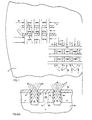
- the chip or die is partly shown at 1 carrying an NPN formation of transistors structures 2 and a separate PNP formation of transistor structures 3.
- a pair of intersecting slots 4 and 5 form triangular shaped active regions 6 and 7 separated by orthogonal slots 8 and 9.
- the arrows 10 and 11 illustrate the angle doping paths (when -tilted upwardly) for N or N+ doping of the underlying substrate.
- slots 8 and 9 are also filled with oxide and electrical connections are established to the electrode regions of the isolated -active transistor regions.
- the intersecting slots 12 and 13 of the P region are illustrated orthogonal to intersecting slots 4 and 5 of the N region 2, and the directions of angled doping, shown by arrows 14 and 15, is at right angles to arrows 10 and 11 of region 2. Since ion milling and ion doping are preferably employed, many regions, such as 2 and 3, may be selectively distributed across the chip 1, and accurately indexed by present day conventional techniques. This offers versatility of association of the complementary transistors. Use of the ullistrated orthogonal relationship of slots 8 and 9 to slots 101 and 102 serves to prevent contaminating of doping (i.e.) N type doping is only Injected at right angles to P type doping.
- substrate 21 is masked by photoresist 23 which is patterned to define the penetration regions for intersecting slots 25 and 26. Since substrate 21 is shown doped N-or P type, the intermediate region 27 will eventually comprise a plurality of transistors of either the NPN or PNP type, having been carved from the substrate by the slots 25 and 26. To prevent intermediate region 27, better defined as a semi-array of transistor regions, from falling into substrate 21, it should be noted that the slots 25 and 26 are interrupted to leave shoulders at spaced apart intervals therealong, best seen at 31, 32 and 33 in Fig. 5.
- the masking layer 23 is a material with a low sputtering rate, such as one of the heavier metals.
- FIGS 3 and 4 illustrate the ease of forming Intersecting slots, such as 25 and 26,simply by orienting the substrate at angles, e.g., 60° to the horizontal, such that the ion flux 37 may remain in its vertical pattern to form, first slots 26, and thereafter slots 25 simply by rotating the substrate 21 through 90°.
- the flux may be accurately directed to any region 2 or 3.
- triangular array 27 is shown as being substantially equilateral, it need not be and the angles may be varied to configure the active regions as desired for specific purposes, It will also be noticed from Figs. 3 and 4 that slots 25 and 26 terminate where they intersect because extending them deeper into the substrate would serve no purpose.
- the slots 25 and 26 may be intermittent such that supporting ribs or webs 31, 32 and 31', 32' serve to support each semi-array 27.
- These webs or supports may be at spaced apart locations along the slots 25 and 26 or merely comprise only supports at the edges of the chips because they serve but a temporary purpose as the slots will be filled with substrate oxide to provide the permanent support for each transistor region.
- the first oxidation step is shown in Fig. 6 wherein silicon oxide 25' and 26' fills the respective slots 25 and 26. Also, an upper layer of silicon oxide 28 (Fig. 6) covers the upper surface and is continguous with the silicon oxide 25' and 26' such that semi-array 27 is totally isolated from the substrate 21 by the silicon oxide, and the periphery of the semi-arrays 27 are substantially covered by the oxide.
- orthogonal slots 41 divide the semi-arrays 27 into the individual transistor regions 27' and provide ingress for the doping to follow.
- each orthogonal slots 41 includes sidewalls 41' through which individual transistor regions 27' will be doped.
- the other sidewalls 41" of slots 41 provide for doping adjacent transistor regions 27'.
- Slots 41 may be ion milled using the masking technique heretofore employed. Consequently, photoresist 43 (fig. 8) of a heavier metal is patterned as shown in Fig. 8 to provide for ion milling slots 41 via the openings 45 in the heavy photoresist 43 and silicon oxide layer 42. The ion flux is illustrated by the lines 46.
- Fig. 8A it may be seen that the N+ regions 31 and 33 are implanted by ion implanting at an angle as illustrated by the ion beams 32 and 34. It is important to note that the angle of the ion beams relative to the slot directions is such that the N+ implanting does not extend to the full depth of the slots 23 and 25. Actually the corners of the silicon oxide layer 42 form a shadowing effect and cooperate with the orientation of the beams 32 and 34 in fixing the N+ doped regions within the P active region 27. Phosphor or other donors may be employed in this step. Dotted lines 31' and 33' show that the doping has been driven in and the N+ regions 31 and 33 considerably enlarged. This may be accomplished through the applica-, tion of heat over a controlled period of time and temperature.
- an individual transistor region 27' is shown comprising N or N+ doped region 51, P or P+ doped region 52 and N or N+ doped region 53.
- the P region 52 is the base region and comprises a portion of the original substrate 21, e.g., doped P.at formation 2 in Fig. 1.
- both N+ regions 51 and 53 are provided by doping region 27' via the sidewalls 41' and 41" of orthogonal slots 41 (Fig. 7) with phosphorous deposition, diffusion or implantation plus drive-in to create the emitter region 51 and the collector region 53.
- the structure of Fig. 9 is oxidized to fill in slots 41 with silicon oxide 54 and provide covering layer 51.
- Fig. 10 The next step in the process is illustrated in Fig. 10 wherein the silicon oxide layer 51 has been patterned to leave oxide islands 55 and metallization applied to comprise the emitter electrode 71, base electrode 72 and collector electrode 73.
- a light boron deposit may be made in the base region 52 to provide the P+ base spanning region 75, if desired.
- the purpose of the boron deposition 75 prior to the metallization is two fold, i.e., first to reduce the base region contact resistance and second to produce a potential barrier P+ that will deflect the electrons in transit across the base region 52 away from the base contact.
- a PNP device can be built utilizing a P-type substrate in the manner of having built the NPN device starting from a P substrate as described in region 3 Fig. 1. This is shown in Fig. 11 wherein emitter region 85 is conventionally P doped, but by angled ion flux via the slots 101, 102 (Fig. 1) just as in the process for the NPN transistors. Collector region 86 is similarly formed, and base region 87 is part of the original N doped substrate 3 (Fig. 1).
- Interconnections of the complementary transistors may be established using conventional diffused lines, poly lines or metal patterning.
- N and P formations need not be at right angles but this arrangement insures that ion doping is carried out most efficiently and there are no components of doping intended for NPN transistors which dope the complementary PNP transistors. This orientation facilitates higher speed and more efficient processing.
Abstract
The invention is a pair of complementary transistors or arrays thereof and method for producing same in sub-micron dimensions on a silicon substrate selectively doped P and N type by forming intersectings slots (4, 5) in spaced apart relation across the P substrate regions to define semi-arrays of V shaped intermediate regions which will become transistors. Silicon oxide fills these slots and separates the NPN transistor regions from the substrate. Orthogonal slots (8, 9) divide the semi-arrays into individual transistor active regions; N doping is then introduced into each active region via the orthogonal slots and driven in to form the emitter and collector regions on respective sides of original substrate which forms the base regions. The same construction obtains in the N substrate regions to form the arrays of PNP transistors. Metallization patterns complete electrical connections to the emitter, base and collector regions and silicon oxide substantially covers the periphery of each active region for total isolation.
Description
- This invention is a novel structure and method for forming sub-micron type lateral dielectrically isolated complementary transistors utilizing VLSI chip processing steps to compatibly fabricate hundreds of such devices, simultaneously on a common functional chip.
- Techniques extracted from the prior art come from the field of sub-micron fabrication technology wherein the dimensional resolution is now comparable to or even smaller than the thicknesses of the thermally grown silicon oxide layers on silicon. Also, the dimensions are now comparable or even smaller than the base widths used for fused transistors, i.e., 0.4 to 1.0 micrometers. From these techniques, the novel structure and method for the complementary lateral transistors with greatly reduced parasitic capacitances and resistances are achieved.
- The invention comprises novel lateral complementary transistors formed on a selectively doped substrate by intersecting slots and orthogonal slots for respectively defining each active region undercut by selective intersecting slots and filled with substrate oxide to isolate the effective regions from the substrate. Prior to oxidation filling the orthogonal slots, selective doping is introduced by angle implantation from opposed orthogonal surfaces of each individual active region to complete the NPN formations or the complementary PNP formations. The intersecting slots and the orthogonal slots of the complementary devices are respectively orthogonally related. Electrical connections are made in conventional fashion to become emitter, base and collector regions.
-
- FIGURE 1 shows a portion of a chip including separate formations of NPN and PNP devices;
- FIGURE 2 is a cross sectional view through the substrate showing the formation of intersecting slots;
- FIGURE 3 shows a substrate oriented at an angle above the horizontal such that vertical milling may form the diagonally penetrating slots;
- FIGURE 4 shows the substrate oppositely oriented to that of FIG. 3 such that vertical milling may again form the other portion of the intersecting slots;
- FIGURE 5 is a view in top plan of the substrate showing the spaced apart intersecting slots with support regions between the ends thereof;
- FIGURE 6 is a front view of the triangular semi-arrays of substrate formed by the intersecting slots and separated from the substrate proper;
- FIGURE 7 shows the introduction of orthogonal slots relative to the pairs of intersecting slots;
- FIGURE 8 shows the formation of the orthogonal slots via milling;
-
- FIGURE 9 is a view of a single active transistor region following N+ doping via the orthogonal slots and prior to oxidation filling the same;
- FIGURE 10 is a view of the structure of FIG. 9 with metallization contacts for the emitter, base and collector regions; and,
- FIGURE 11 shows a PNP active region, per se.
- In the devices produced in accordance with the present invention, the effects of the substrate are minimized relative to the operation of the devices. It should be realized that the isolated active region may be completely contained within a surface area of approximately 5d x 3d = 15d2 wherein d is only 0.4 micrometers. Each active region is completely separated from the substrate by substrate oxidation and the parasitic capacitances and resistances are almost completely reduced to a minimum value attainable because the transistors are reduced to just their electronically active regions. In the conventional (vertical) transistor, the electrically active region is only a very small fraction of the total transistor area or volume. The dielectric isolation between transistors offered by the substrate oxidation has advantages with respect to high frequency performance, high voltage integrated circuits, radiation resistance, and circuit flexibility, i.e., the process provides NPN and PNP devices on the same integrated circuit chip.
- In Figure 1, the chip or die is partly shown at 1 carrying an NPN formation of
transistors structures 2 and a separate PNP formation oftransistor structures 3. - In
formation 2, a pair of intersectingslots 4 and 5 form triangular shapedactive regions orthogonal slots arrows 10 and 11 illustrate the angle doping paths (when -tilted upwardly) for N or N+ doping of the underlying substrate. Subsequently,slots - In
formation 3, theintersecting slots slots 4 and 5 of theN region 2, and the directions of angled doping, shown byarrows arrows 10 and 11 ofregion 2. Since ion milling and ion doping are preferably employed, many regions, such as 2 and 3, may be selectively distributed across the chip 1, and accurately indexed by present day conventional techniques. This offers versatility of association of the complementary transistors. Use of the ullistrated orthogonal relationship ofslots slots 101 and 102 serves to prevent contaminating of doping (i.e.) N type doping is only Injected at right angles to P type doping. - Referring now to Figure 2,
substrate 21 is masked byphotoresist 23 which is patterned to define the penetration regions for intersectingslots substrate 21 is shown doped N-or P type, theintermediate region 27 will eventually comprise a plurality of transistors of either the NPN or PNP type, having been carved from the substrate by theslots intermediate region 27, better defined as a semi-array of transistor regions, from falling intosubstrate 21, it should be noted that theslots - Since the preferred way of forming
slots flux lines 37 in Fig. 2, themasking layer 23 is a material with a low sputtering rate, such as one of the heavier metals. - Figures 3 and 4 illustrate the ease of forming Intersecting slots, such as 25 and 26,simply by orienting the substrate at angles, e.g., 60° to the horizontal, such that the
ion flux 37 may remain in its vertical pattern to form,first slots 26, and thereafterslots 25 simply by rotating thesubstrate 21 through 90°. The flux may be accurately directed to anyregion - While the
triangular array 27 is shown as being substantially equilateral, it need not be and the angles may be varied to configure the active regions as desired for specific purposes, It will also be noticed from Figs. 3 and 4 thatslots - From Fig. 5, it may be seen that the
slots webs semi-array 27. These webs or supports may be at spaced apart locations along theslots - The first oxidation step is shown in Fig. 6 wherein
silicon oxide 25' and 26' fills therespective slots silicon oxide 25' and 26' such thatsemi-array 27 is totally isolated from thesubstrate 21 by the silicon oxide, and the periphery of thesemi-arrays 27 are substantially covered by the oxide. - In Fig. 7,
orthogonal slots 41 divide thesemi-arrays 27 into the individual transistor regions 27' and provide ingress for the doping to follow. Thus, eachorthogonal slots 41 includes sidewalls 41' through which individual transistor regions 27' will be doped. Theother sidewalls 41" ofslots 41 provide for doping adjacent transistor regions 27'.Slots 41 may be ion milled using the masking technique heretofore employed. Consequently, photoresist 43 (fig. 8) of a heavier metal is patterned as shown in Fig. 8 to provide forion milling slots 41 via theopenings 45 in theheavy photoresist 43 andsilicon oxide layer 42. The ion flux is illustrated by thelines 46. - In Fig. 8A, it may be seen that the
N+ regions ion beams 32 and 34. It is important to note that the angle of the ion beams relative to the slot directions is such that the N+ implanting does not extend to the full depth of theslots silicon oxide layer 42 form a shadowing effect and cooperate with the orientation of thebeams 32 and 34 in fixing the N+ doped regions within the Pactive region 27. Phosphor or other donors may be employed in this step. Dotted lines 31' and 33' show that the doping has been driven in and theN+ regions - In Figure 9, an individual transistor region 27' is shown comprising N or N+ doped
region 51, P or P+ dopedregion 52 and N or N+ dopedregion 53. TheP region 52 is the base region and comprises a portion of theoriginal substrate 21, e.g., dopedP.at formation 2 in Fig. 1. However, bothN+ regions sidewalls 41' and 41" of orthogonal slots 41 (Fig. 7) with phosphorous deposition, diffusion or implantation plus drive-in to create theemitter region 51 and thecollector region 53. Thereafter, the structure of Fig. 9 is oxidized to fill inslots 41 withsilicon oxide 54 and provide coveringlayer 51. - The next step in the process is illustrated in Fig. 10 wherein the
silicon oxide layer 51 has been patterned to leaveoxide islands 55 and metallization applied to comprise theemitter electrode 71,base electrode 72 andcollector electrode 73. However, prior to applying the metallization, a light boron deposit may be made in thebase region 52 to provide the P+base spanning region 75, if desired. - The purpose of the
boron deposition 75 prior to the metallization is two fold, i.e., first to reduce the base region contact resistance and second to produce a potential barrier P+ that will deflect the electrons in transit across thebase region 52 away from the base contact. - Finally, a PNP device can be built utilizing a P-type substrate in the manner of having built the NPN device starting from a P substrate as described in
region 3 Fig. 1. This is shown in Fig. 11 whereinemitter region 85 is conventionally P doped, but by angled ion flux via theslots 101, 102 (Fig. 1) just as in the process for the NPN transistors.Collector region 86 is similarly formed, andbase region 87 is part of the original N doped substrate 3 (Fig. 1). - Patterning of the silicon oxide on the top of this complementary device has been shown and it is only necessary to lay down the metallization pattern for electrical connection to the various transistor regions.
- Interconnections of the complementary transistors may be established using conventional diffused lines, poly lines or metal patterning.
- It should be mentioned that the N and P formations need not be at right angles but this arrangement insures that ion doping is carried out most efficiently and there are no components of doping intended for NPN transistors which dope the complementary PNP transistors. This orientation facilitates higher speed and more efficient processing.
- The dielectrically isolated complementary transistors of this invention have no junction curvature and thus exhibit higher breakdown voltages. Also, they exhibit very low capacitances, i.e., Ccb, Cbe, and Ccs. Similarly, bulk resistance is very low (i.e.) rbb', rcc' and reel. Symmetrical transistors are readily available with very low VCE at Ic = 0. Also available is high β at low current levels (4 /MA), with no current crowding at the higher current levels. By the use of oversize geometry, close control over transistor parameters is possible with respect to the absolute values, and more importantly, the matching tolerances, partly due to the excellent control available with respect to base width since it is now a function of lateral geometry and not of the small differences of two diffusions as in conventional double diffused transistors.
Claims (12)
1. An array of sub-micron dimensioned complementary NPN and PNP type lateral transistors formed on a silicon substrate doped P and N type, comprising in combination:
a plurality of first sidewalls of pairs of intersecting slots in spaced apart relation across the P regions of the substrate defining-semi-arrays of V shaped intermediate regions which will become transistors;
silicon oxide filling said slots and covering the surface of the substrate through which they were made;
a plurality of second sidewalls of orthogonal slots relative to said pairs of slots dividing the semi-arrays of regions into individual transistor active regions;
selective doping introduced into said active regions via said second sidewalls and driven in to comprise emitter and collector regions on respective sides of original P and N substrate comprising the respective base regions;
metallization patterns in electrical connection with the respective-emitter, base and collector regions; and,
silicon oxide at least substantially covering the periphery of each active region.
2. Transistor arrays in accordance with claim 1, wherein:
said intersecting slots for the NPN transistors are normal to said intersecting slots for the PNP transistors; and,
said orthogonal slots for the NPN transistors are normal to said orthogonal slots for the PNP transistors.
3. The transistor arrays in accordance with claims 1 and 2, wherein:
said selective doping comprises N doping for the P substrate regions and P doping for the N substrate regions.
4. An array of sub-micron dimensioned PNP and NPN type lateral complementary transistors formed on a silicon substrate selectively doped N and P type in different substrate regions, comprising in combination:
a plurality of first sidewalls of pairs of intersecting slots in spaced apart relation across N doped regions of the substrate defining semi-arrays of V shaped intermediate regions which will become PNP transistors;
a second plurality of sidewalls orthogonal to said first sidewalls comprising further pairs of Intersecting slots in spaced apart relation across P doped regions of the substrate defining semi-arrays of V shaped intermediate regions which will become NPN transistors;
silicon oxide filling said slots and covering the surface of the substrate through which they were made;
a plurality of second sidewalls of orthogonal slots relative to said pairs of slots dividing the semi-arrays of regions into individual transistor active regions;
N and P doping selectively introduced into selected ones of said active regions via said second sidewalls and driven in to comprise emitter and collector regions on respective sides of original N or P substrate comprising the base regions;
metallization patterns in electrical connection with the respective emitter, base and collector regions; and,
silicon oxide at least substantially covering the periphery of each active region.
5. A method for producing an array of sub-micron dimensioned PNP and NPN type lateral complementary transistors formed on a silicon substrate selectively doped N and P type, comprising the steps of:
forming a plurality of first sidewalls of pairs of intersecting slots in spaced apart relation across N regions of the substrate defining semi-arrays of V shaped intermediate regions which will become transistors;
forming a plurality of first sidewalls of pairs of Intersecting slots in spaced apart relation across P regions of the substrate defining semi-arrays of V shaped intermediate regions which will become transistors;
oxidizing the substrate and intermediate regions to fill said slots and cover the surface of the substrate through which they were made;
forming a plurality of second sidewalls of orthogonal slots relative to said pairs of slots dividing the semi-arrays of regions into individual NPN and PNP transistor active regions;
N or P doping selected ones of said active regions via said second sidewalls;
driving in said doping to comprise emitter and collector regions on respective sides of original P and N substrate comprising the base regions; and,
forming metallization patterns in electrical connection with at least the respective emitter, base and collector regions.
6. A method for producing an array of sub-micron dimensioned NPN and PNP type lateral complementary transistors formed on a silicon substrate doped selectively P and N-type, comprising the steps of:
forming a plurality of first sidewalls of pairs of intersecting slots in spaced apart relation across the N regions of the substrate defining semi-arrays of V shaped intermediate regions which will become PNP transistors;
forming a second plurality of first sidewalls of pairs of intersecting slots in spaced apart relation across the P regions of the substrate defining semi-arrays of V shaped intermediate regions which will become NPN transistors;
said second plurality of first sidewalls being normal to said first sidewalls of the first mentioned plurality but do not intersect them;
oxidizing the substrate and intermediate regions to fill said slots and cover the surface of the substrate through which they were made;
forming a plurality of second sidewalls of orthogonal slots relative to said first mentioned pairs of slots dividing the semi-arrays of regions into individual transistor active regions;
P doping each of said active regions via said second sidewalls;
forming a second plurality of second sidewalls of further orthogonal slots relative to said second plurality of first sidewalls of pairs of intersecting slots dividing the semi-arrays of regions into individual transistor active regions; '
N doping each of said last mentioned active regions via said further orthogonal slots;
driving in said doping to comprise emitter and collector regions on respective sides of original N and P substrate comprising the base regions; and,
forming metallization patterns in electrical connection - with at least the respective emitter, base and collector regions.
7. A method for producing arrays of sub-micron dimensioned lateral complementary transistors formed on a silicon substrate selectively doped P and N type, comprising the steps of:
forming a plurality of first pairs of intersecting slots in spaced apart relation across the selective N portions of the substrate defining semi-arrays of V shaped intermediate regions which will become PNP transistors;
forming a plurality of second pairs of intersecting slots in spaced apart relation across the selective P portions of the substrate defining semi-arrays of V shaped intermediate regions which will become NPN transistors;
said second pairs being normal to said first pairs and out of contact therewith;
silicon oxide filling said slots and covering the surface of the substrate through which they were made;
forming a plurality of orthogonal slots relative to said first pairs of slots dividing the semi-arrays of N regions into individual PNP transistor active regions;
P doping each of said N active regions via said orthogonal slots;
forming a second plurality of orthogonal slots relative to said second pairs of slots dividing the semi-arrays of P regions into individual NPN transistor active regions;
N doping each of said P active regions via the second plurality of orthogonal slots; .
driving in said doping to comprise emitter and collector regions on respective sides of original substrate comprising the base regions; and,
forming conductor patterns in electrical connection with the respective emitter, base and collector regions.
8. A pair of NPN PNP complementary transistors formed on a common substrate, comprising in combination:
an N doped portion of said substrate;
a pair of intersecting slots in said portion filled with substrate oxide defining the length of the PNP transistor;
an orthogonal pair of slots in said N portion relative to said intersecting slots through which P doping is driven into the ends of said PNP transistor to comprise the collector and emitter respectively, said base being comprised of N doped substrate;
said orthogonal slots filled with substrate oxide;
a P doped portion of said substrate;
a second pair of intersecting slots in said P portion filled with substrate oxide defining the length of the NPN transistor;
a second pair of orthogonal slots in said P portion i relative to said second pair of intersecting slots through which N doping is driven into the ends of said NPN transistor to comprise the collector and emitter respectively, said base being comprised of P doped substrate;
said second pair of orthogonal slots filled with substrate oxide; and,
conductors in electrical connection with at least said emitters, bases, and collectors.
9. Complementary transistors each having an active region formed on a common substrate, comprising the steps of:
recessing the substrate substantially along the periphery of each transistor active region;
selectively doping the transistor active regions through portions of the recesses formed by said recessing;
at least partly filling said recesses with substrate oxide to isolate the active regions from said substrate; and,
forming conductors to different portions of each active region to serve as electrode connections.
10. The complementary transistors of Claim 9, wherein:
said doping is accomplished by ion bombardment into electrode portions of said active regions via said portions of said recesses at an angle of less than 90° relative to the substrate.
11. The complementary transistors of Claim 10, wherein:
said rece-sing separates said active regions from the substrate; and,
said substrate oxide envelopes each active region.
Applications Claiming Priority (2)
| Application Number | Priority Date | Filing Date | Title |
|---|---|---|---|
| US27746581A | 1981-06-25 | 1981-06-25 | |
| US277465 | 1981-06-25 |
Publications (1)
| Publication Number | Publication Date |
|---|---|
| EP0069191A1 true EP0069191A1 (en) | 1983-01-12 |
Family
ID=23060993
Family Applications (1)
| Application Number | Title | Priority Date | Filing Date |
|---|---|---|---|
| EP82101439A Withdrawn EP0069191A1 (en) | 1981-06-25 | 1982-02-25 | Complementary NPN and PNP lateral transistors separated from substrate by intersecting slots filled with substrate oxide for minimal interference therefrom and method for producing same |
Country Status (2)
| Country | Link |
|---|---|
| EP (1) | EP0069191A1 (en) |
| JP (1) | JPS583279A (en) |
Cited By (3)
| Publication number | Priority date | Publication date | Assignee | Title |
|---|---|---|---|---|
| EP0512607A2 (en) * | 1991-05-03 | 1992-11-11 | Koninklijke Philips Electronics N.V. | Method of manufacturing a semiconductor device using ion implantation |
| US5405454A (en) * | 1992-03-19 | 1995-04-11 | Matsushita Electric Industrial Co., Ltd. | Electrically insulated silicon structure and producing method therefor |
| US5855493A (en) * | 1996-03-11 | 1999-01-05 | The Whitaker Corporation | Electrical connector strain relief with shield ground for multiple cables |
Families Citing this family (1)
| Publication number | Priority date | Publication date | Assignee | Title |
|---|---|---|---|---|
| EP0068070A1 (en) * | 1981-07-01 | 1983-01-05 | Rockwell International Corporation | Complementary NPN and PNP lateral transistors separated from substrate by slots filled with substrate oxide for minimal interference therefrom and method for producing same |
Citations (3)
| Publication number | Priority date | Publication date | Assignee | Title |
|---|---|---|---|---|
| US4104090A (en) * | 1977-02-24 | 1978-08-01 | International Business Machines Corporation | Total dielectric isolation utilizing a combination of reactive ion etching, anodic etching, and thermal oxidation |
| EP0004298A1 (en) * | 1978-03-02 | 1979-10-03 | Western Electric Company, Incorporated | Method of fabricating isolation of and contact to burried layers of semiconductor structures |
| US4214315A (en) * | 1979-03-16 | 1980-07-22 | International Business Machines Corporation | Method for fabricating vertical NPN and PNP structures and the resulting product |
-
1982
- 1982-02-25 EP EP82101439A patent/EP0069191A1/en not_active Withdrawn
- 1982-06-17 JP JP57106068A patent/JPS583279A/en active Pending
Patent Citations (3)
| Publication number | Priority date | Publication date | Assignee | Title |
|---|---|---|---|---|
| US4104090A (en) * | 1977-02-24 | 1978-08-01 | International Business Machines Corporation | Total dielectric isolation utilizing a combination of reactive ion etching, anodic etching, and thermal oxidation |
| EP0004298A1 (en) * | 1978-03-02 | 1979-10-03 | Western Electric Company, Incorporated | Method of fabricating isolation of and contact to burried layers of semiconductor structures |
| US4214315A (en) * | 1979-03-16 | 1980-07-22 | International Business Machines Corporation | Method for fabricating vertical NPN and PNP structures and the resulting product |
Cited By (5)
| Publication number | Priority date | Publication date | Assignee | Title |
|---|---|---|---|---|
| EP0512607A2 (en) * | 1991-05-03 | 1992-11-11 | Koninklijke Philips Electronics N.V. | Method of manufacturing a semiconductor device using ion implantation |
| EP0512607A3 (en) * | 1991-05-03 | 1993-09-08 | N.V. Philips' Gloeilampenfabrieken | Method of manufacturing a semiconductor device using ion implantation |
| US5405454A (en) * | 1992-03-19 | 1995-04-11 | Matsushita Electric Industrial Co., Ltd. | Electrically insulated silicon structure and producing method therefor |
| US5543351A (en) * | 1992-03-19 | 1996-08-06 | Matsushita Electric Industrial Co., Ltd. | Method of producing electrically insulated silicon structure |
| US5855493A (en) * | 1996-03-11 | 1999-01-05 | The Whitaker Corporation | Electrical connector strain relief with shield ground for multiple cables |
Also Published As
| Publication number | Publication date |
|---|---|
| JPS583279A (en) | 1983-01-10 |
Similar Documents
| Publication | Publication Date | Title |
|---|---|---|
| US4437226A (en) | Process for producing NPN type lateral transistor with minimal substrate operation interference | |
| US4038680A (en) | Semiconductor integrated circuit device | |
| US4466178A (en) | Method of making extremely small area PNP lateral transistor by angled implant of deep trenches followed by refilling the same with dielectrics | |
| US4458158A (en) | IC Including small signal and power devices | |
| US4419150A (en) | Method of forming lateral bipolar transistors | |
| US4115797A (en) | Integrated injection logic with heavily doped injector base self-aligned with injector emitter and collector | |
| JPH0336311B2 (en) | ||
| US4522682A (en) | Method for producing PNP type lateral transistor separated from substrate by O.D.E. for minimal interference therefrom | |
| US4415371A (en) | Method of making sub-micron dimensioned NPN lateral transistor | |
| EP0068071A1 (en) | Punch through voltage regulator diodes and methods of manufacture | |
| US4988639A (en) | Method of manufacturing semiconductor devices using trench isolation method that forms highly flat buried insulation film | |
| KR0139005B1 (en) | Merged complementary bipolar and mos means and its manufacturing method | |
| US4584762A (en) | Lateral transistor separated from substrate by intersecting slots filled with substrate oxide for minimal interference therefrom and method for producing same | |
| KR890003474B1 (en) | Lateral bipolar tr forming on soi plate | |
| US4485551A (en) | NPN Type lateral transistor separated from substrate by O.D.E. for minimal interference therefrom and method for producing same | |
| US4435899A (en) | Method of producing lateral transistor separated from substrate by intersecting slots filled with substrate oxide | |
| EP0069191A1 (en) | Complementary NPN and PNP lateral transistors separated from substrate by intersecting slots filled with substrate oxide for minimal interference therefrom and method for producing same | |
| US5198376A (en) | Method of forming high performance lateral PNP transistor with buried base contact | |
| EP0059264A1 (en) | NPN Type lateral transistor with minimal substrate operation interference and method for producing same | |
| US4704786A (en) | Method of forming a lateral bipolar transistor in a groove | |
| JPH0413863B2 (en) | ||
| US4506283A (en) | Small area high value resistor with greatly reduced parasitic capacitance | |
| US4497685A (en) | Small area high value resistor with greatly reduced parasitic capacitance | |
| US5031014A (en) | Lateral transistor separated from substrate by intersecting slots filled with substrate oxide for minimal interference therefrom | |
| EP0059266A2 (en) | Lateral transistor separated from substrate by intersecting slots filled with a substrate oxide for minimal interference therefrom and method for producing same |
Legal Events
| Date | Code | Title | Description |
|---|---|---|---|
| PUAI | Public reference made under article 153(3) epc to a published international application that has entered the european phase |
Free format text: ORIGINAL CODE: 0009012 |
|
| 17P | Request for examination filed |
Effective date: 19820630 |
|
| AK | Designated contracting states |
Designated state(s): DE FR GB |
|
| STAA | Information on the status of an ep patent application or granted ep patent |
Free format text: STATUS: THE APPLICATION IS DEEMED TO BE WITHDRAWN |
|
| 18D | Application deemed to be withdrawn |
Effective date: 19840830 |
|
| RIN1 | Information on inventor provided before grant (corrected) |
Inventor name: SOCLOF, SIDNEY ISAAC |