EP0070737A2 - Semiconductor device having an electrode, and method for producing the same - Google Patents
Semiconductor device having an electrode, and method for producing the same Download PDFInfo
- Publication number
- EP0070737A2 EP0070737A2 EP82303828A EP82303828A EP0070737A2 EP 0070737 A2 EP0070737 A2 EP 0070737A2 EP 82303828 A EP82303828 A EP 82303828A EP 82303828 A EP82303828 A EP 82303828A EP 0070737 A2 EP0070737 A2 EP 0070737A2
- Authority
- EP
- European Patent Office
- Prior art keywords
- contact electrode
- insulating layer
- conductor line
- polycrystalline silicon
- layer
- Prior art date
- Legal status (The legal status is an assumption and is not a legal conclusion. Google has not performed a legal analysis and makes no representation as to the accuracy of the status listed.)
- Granted
Links
Images


Classifications
-
- H—ELECTRICITY
- H01—ELECTRIC ELEMENTS
- H01L—SEMICONDUCTOR DEVICES NOT COVERED BY CLASS H10
- H01L21/00—Processes or apparatus adapted for the manufacture or treatment of semiconductor or solid state devices or of parts thereof
- H01L21/70—Manufacture or treatment of devices consisting of a plurality of solid state components formed in or on a common substrate or of parts thereof; Manufacture of integrated circuit devices or of parts thereof
- H01L21/71—Manufacture of specific parts of devices defined in group H01L21/70
- H01L21/768—Applying interconnections to be used for carrying current between separate components within a device comprising conductors and dielectrics
- H01L21/76838—Applying interconnections to be used for carrying current between separate components within a device comprising conductors and dielectrics characterised by the formation and the after-treatment of the conductors
- H01L21/7684—Smoothing; Planarisation
-
- H—ELECTRICITY
- H01—ELECTRIC ELEMENTS
- H01L—SEMICONDUCTOR DEVICES NOT COVERED BY CLASS H10
- H01L21/00—Processes or apparatus adapted for the manufacture or treatment of semiconductor or solid state devices or of parts thereof
- H01L21/70—Manufacture or treatment of devices consisting of a plurality of solid state components formed in or on a common substrate or of parts thereof; Manufacture of integrated circuit devices or of parts thereof
- H01L21/71—Manufacture of specific parts of devices defined in group H01L21/70
- H01L21/768—Applying interconnections to be used for carrying current between separate components within a device comprising conductors and dielectrics
- H01L21/76838—Applying interconnections to be used for carrying current between separate components within a device comprising conductors and dielectrics characterised by the formation and the after-treatment of the conductors
- H01L21/76877—Filling of holes, grooves or trenches, e.g. vias, with conductive material
- H01L21/7688—Filling of holes, grooves or trenches, e.g. vias, with conductive material by deposition over sacrificial masking layer, e.g. lift-off
-
- H—ELECTRICITY
- H01—ELECTRIC ELEMENTS
- H01L—SEMICONDUCTOR DEVICES NOT COVERED BY CLASS H10
- H01L23/00—Details of semiconductor or other solid state devices
- H01L23/48—Arrangements for conducting electric current to or from the solid state body in operation, e.g. leads, terminal arrangements ; Selection of materials therefor
- H01L23/482—Arrangements for conducting electric current to or from the solid state body in operation, e.g. leads, terminal arrangements ; Selection of materials therefor consisting of lead-in layers inseparably applied to the semiconductor body
- H01L23/485—Arrangements for conducting electric current to or from the solid state body in operation, e.g. leads, terminal arrangements ; Selection of materials therefor consisting of lead-in layers inseparably applied to the semiconductor body consisting of layered constructions comprising conductive layers and insulating layers, e.g. planar contacts
-
- H—ELECTRICITY
- H01—ELECTRIC ELEMENTS
- H01L—SEMICONDUCTOR DEVICES NOT COVERED BY CLASS H10
- H01L2924/00—Indexing scheme for arrangements or methods for connecting or disconnecting semiconductor or solid-state bodies as covered by H01L24/00
- H01L2924/0001—Technical content checked by a classifier
- H01L2924/0002—Not covered by any one of groups H01L24/00, H01L24/00 and H01L2224/00
Definitions
- the present invention relates to a semiconductor device and a method for producing the same. More particularly, it relates to an interconnection structure in a semiconductor device, such as an integrated circuit (IC) device or a large-scale integration (LSI) device.
- IC integrated circuit
- LSI large-scale integration
- the conductor pattern comprises conductor lines (i.e., wirings) lying on an insulating layer of, e.g., phosphosilicate glass (PSG) or silicon dioxide (Si0 2 ) and making contact through small apertures (i.e., contact holes) in the insulating layer with the underlying device portion (e.g., a portion of the semiconductor substrate) or with the other,underlyingconductor line.
- conductor lines i.e., wirings
- PSG phosphosilicate glass
- Si0 2 silicon dioxide
- a conductive layer e.g., an aluminum layer
- a conductor pattern i.e. a desired pattern of conductor lines
- an insulating layer 1 (e.g., PSG) formed on semiconductor substrate 2 (e.g., a silicon wafer) is selectively etched by a conventional photoetching method using photoresist layer 3 to form contact hole 4.
- conductive material e.g., aluminum
- photoresist layer 3 and conductive layer 5b are simultaneously removed with a suitable solvent. This removal process is referred to as the lift off process.
- Wedge gap 6 (Fig. 3) is formed between contact electrode 5a and the side of insulating layer 1.
- Fig. 3 is formed between contact electrode 5a and the side of insulating layer 1.
- a semiconductor device comprises an insulating layer
- a conductor line is formed without a break or a thin portion.
- a method of producing a semiconductor device comprises the steps of forming an insulating layer on a semiconductor substrate or a conductor line; opening a contact hole in the insulating layer ; forming a contact electrode in the contact hole; and forming a conductor line on the contact electrode and insulating layer and is characterised in that the method further comprises the steps of filling a gap between the contact electrode and the side of the insulating layer with polycrystàline silicon prior to the formation of the conductor line; and alloying the polycrystalline silicon with at least one of the conductor line formed on the contact electrode and the contact electrode,by heating.
- the contact electrode may be arranged on another conductor line instead of a semiconductor substrate.
- an insulating layer 11 (e.g. PSG or Si0 2 ) is formed on a semiconductor substrate 12 (e.g. a silicon wafer).
- a photoresist layer 13 is coated on insulating layer 11, is exposed, and is developed to form a photoresist pattern having a through hole.
- Insulating layer 11 is selectively etched with a suitable etchant through the through hole to form a contact hole (i.e., a through aperture).
- a high-melting point metal such as molybdenum (Mo), tantalum (Ta), titanium (Ti), tungsten (W), or platinum (Pt) is deposited on photoresist layer 13 and on the exposed portion of semiconductor substrate 12 by a sputtering method to form metal layer 14a and contact electrode 14b.
- Mo molybdenum
- Ta tantalum
- Ti titanium
- W tungsten
- Pt platinum
- Photoresist layer 13 is removed with a suitable solvent, and, therefore, metal layer 14a can be removed.
- polycrystalline silicon is deposited on the surfaces of insulating layer 11 and contact electrode 14b by a low-pressure chemical vapour deposition (C V D) method to form polycrystalline silicon layer 16.
- C V D chemical vapour deposition
- the thermal decomposition of silane (SiH 4 ) or the reduction of SiC14 (or SiH 2 C1 2 ) with hydrogen is carried out at a reaction temperature of from 600°C to 700°C so that it is impossible to use aluminum (Al) for contact electrode 14b.
- the wedge gap 15 can be completely filled with the polycrystalline silicon.
- Polycrystalline silicon layer 16 is etched to expose the surface of insulating layer 11 by a dry etching method, such as a reactive sputter etching method, as illustrated in Fig. 7. If the thickness of contact electrode 14b is equal to that of insulating layer 11, the surface of contact electrode 14b is also exposed. Wedge-shaped polycrystalline silicon portion 16a remains in the wedge gap so that a substantially level surface of the entire layer comprising insulating layer 11, contact electrode 14b, and wedge polycrystalline silicon portion 16a can be obtained.
- a dry etching method such as a reactive sputter etching method
- Al is deposited on the level surface (i.e., on the surface of insulating layer 11, wedge polycrystalline silicon portion 16a, and contact electrode 14b) by a vacuum evaporation method to form a conductor layer 17 without causing cracks to form.
- Conductor (Al) layer 17 is selectively etched by a conventional photoetching method to form a conductor line for interconnection. It is possible to use one of the above-mentioned high-melting point metals, such as Mo, Ta, Ti, W, or Pt, instead of Al. In this case, conductor layer 17 is formed by sputtering the high-melting point metal.
- the resultant device is heated so as to alloy wedge polycrystalline silicon portion 16a with the conductor line- and/or contact electrode 14b.
- the heating temperature is approximately 400°C to 500°C in the case of the Al conductor line and is from 900°C to 1000°C in the case of the high-melting point melt conductor line.
- Contact electrode 14b and the alloy of polycrystalline silicon portion 16a ensure an ohmic contact between conductor line and semiconductor substrate 12. Thus, a semiconductor device having a conductor line free of cracks can be produced.
- the alloying is carried out during the formation of PSG by the CVD method.
- a contact hole is formed in insulating layer 21 lying on semiconductor substrate 22 in the same manner as that of the first embodiment.
- the photoresist layer (not shown) on insulating layer 21 is removed with a suitable solvent.
- One of the above-mentioned high-melting point metals is deposited on insulating layer 21 and on the exposed portion of semiconductor substrate 22 by a sputtering method to form metal layer 23a and contact electrode 23b, respectively.
- Wedge gap 24 is formed between contact electrode 23b and the side of insulating layer 21.
- polycrystalline silicon is deposited on the surfaces of metal layer 23a and contact electrode 23b by a low-pressure CVD method to form polycrystalline silicon layer 25.
- the wedge gap is filled with polycrystalline silicon layer 25.
- polycrystalline silicon layer 25 and metal layer 23a are etched by a dry etching method so as to expose the surface of insulating layer 21.
- the obtained structure having a level surface is the same as that illustrated in Fig. 7.
- a conductor line of Al or of one of the above-mentioned high-melting point metals is formed and then a heat treatment for alloying of the portion of polycrystalline silicon layer 25 remaining in the wedge gap with the conductor line and/or contact electrode 23b is carried out in the same manner as that of the first embodiment.
- a heat treatment for alloying of the portion of polycrystalline silicon layer 25 remaining in the wedge gap with the conductor line and/or contact electrode 23b is carried out in the same manner as that of the first embodiment.
- a contact hole is formed in insulating layer 31 lying on semiconductor substrate 32 in the same manner as that of the first embodiment.
- the photoresist layer (not shown) on insulating layer 31 is removed with a suitable solvent.
- Thin polycrystalline silicon layer 33 is formed on the exposed surfaces of insulating layer 31 and semiconductor substrate 32 by a low-pressure CVD method.
- the polycrystalline silicon layer 33 is heavily doped as deposited or by means of thermal impurity diffusion or ion implantation after the deposition.
- one of the above--mentioned high-melting point metals is deposited on thin polycrystalline silicon layer 33 by a sputtering method so that metal layer 34a and contact electrode 34b are formed.
- Contact electrode 34b is positioned within a blind hole of thin silicon layer 33, and a wedge gap is formed between contact electrode 34b and the vertical surface of thin silicon layer 33.
- the thicknesses of insulating layer 31, thin polycrystalline silicon layer 33, and metal layer 34a are approximately 800 nm, approximately 100 nm, and from 400 to 700 nm, respectively.
- Polycrystalline silicon is deposited on the entire exposed surface by a low-pressure CVD method to form polycrystalline silicon layer 35, with which the wedge gap is filled.
- polycrystalline silicon layer 35, metal layer 34a, and thin polycrystalline silicon layer 33 are etched by a dry etching method so as to expose the surface of insulating layer 31. Portion 35a of silicon layer 35 remains in the wedge gap.
- a conductor line (not shown) consisting of a high--melting point metal is formed by using a sputtering method and a photoetching method and then a heat treatment for alloying the polycrystalline silicon of wedge portion 35a and remaining thin layer 33 with the high-melting point metal of the conductor line and contact electrode 34b is carried out in the same manner as that of the first embodiment.
- a conductor line is made of Al
- the heat-treatment conditions are, for example, a heating temperature of 1000°C and a heating time of ten minutes.
- the Al conductor line is subjected to a heat treatment (annealing) at approximately 400°C to 500°C.
Abstract
Description
- The present invention relates to a semiconductor device and a method for producing the same. More particularly, it relates to an interconnection structure in a semiconductor device, such as an integrated circuit (IC) device or a large-scale integration (LSI) device.
- In order to make a semiconductor device (an IC or LSI device) denser, active elements (e.g., transistors) and passive elements (e.g., resistors and condensers) in the semiconductor device are made smaller, and the conductor pattern for electrically interconnecting the elements is made finer. The conductor pattern comprises conductor lines (i.e., wirings) lying on an insulating layer of, e.g., phosphosilicate glass (PSG) or silicon dioxide (Si02) and making contact through small apertures (i.e., contact holes) in the insulating layer with the underlying device portion (e.g., a portion of the semiconductor substrate) or with the other,underlyingconductor line.
- In a case where a conductive layer (e.g., an aluminum layer) is formed by a vacuum evaporation method and is photoengraved to form a conductor pattern, i.e. a desired pattern of conductor lines, cracks form in the conductor line at the contact hole edge, and, as a result, breakage or disconnection of the conductor line can occur or the resistance value of the conductor line can increase.
- In order to form a conductor line without the above--mentioned disadvantage, it is attempted to round a relatively sharp edge of the contact hole by heating the insulating layer, consisting of, e.g., PSG, to its softening point. In this case, however, this heat treatment causes impurities doped in the diffused region of the semiconductor substrate to diffuse, and, thereby, the diffused region expands undesirably. It is also attempted to deposit conductive material (i.e., a contact electrode) in the contact hole only and then form the conductor line on the contact electrode and on the insulating layer. In the latter attempt, as illustrated in Fig. 1, an insulating layer 1 (e.g., PSG) formed on semiconductor substrate 2 (e.g., a silicon wafer) is selectively etched by a conventional photoetching method using
photoresist layer 3 to formcontact hole 4. As illustrated in Fig. 2, conductive material (e.g., aluminum) is deposited onphotoresist layer 3 and the exposed surface ofsubstrate 2 by a vacuum evaporation method to formcontact electrode 5a andconductive layer 5b. Then, as illustrated in Fig. 3,photoresist layer 3 andconductive layer 5b are simultaneously removed with a suitable solvent. This removal process is referred to as the lift off process. Wedge gap 6 (Fig. 3) is formed betweencontact electrode 5a and the side of insulating layer 1. As illustrated in Fig. 4, when conductive material (e.g., aluminum) is deposited on insulating layer 1 and oncontact electrode 5a by a vapour evaporation method to formconductor layer 7, cracks 8 form inconductor layer 7 depending on the circumstances. Accordingly,conductor layer 7 having cracks is patterned by a photoetching method to form a- conductor line having a defect, such as a break or a thin portion. In this case, the possibility of the occurrence of breaks is not as great as in the case where a conductor line is formed without using a contact electrode. In accordance with one aspect of the present invention, a semiconductor device comprises an insulating layer - which is formed on a semiconductor substrate or a conductor line and is provided with a contact hole therein; a contact electrode formed in the contact hole; and a conductor line lying on the contact electrode and on the insulating layer and is characterised in that a gap between the contact electrode and the side of the insulating layer is filled with an alloy of polycrystalline silicon and at least one of the conductor line lying on the contact electrode and the contact electrode.
- With the invention a conductor line is formed without a break or a thin portion.
- In accordance with another aspect of the present invention, a method of producing a semiconductor device comprises the steps of forming an insulating layer on a semiconductor substrate or a conductor line; opening a contact hole in the insulating layer ; forming a contact electrode in the contact hole; and forming a conductor line on the contact electrode and insulating layer and is characterised in that the method further comprises the steps of filling a gap between the contact electrode and the side of the insulating layer with polycrystàline silicon prior to the formation of the conductor line; and alloying the polycrystalline silicon with at least one of the conductor line formed on the contact electrode and the contact electrode,by heating.
- In one example using this method, the contact electrode may be arranged on another conductor line instead of a semiconductor substrate.
- An example of a prior art device and method, and some examples of devices and methods in accordance with the present invention are illustrated in the accompanying drawings, in which:-
- Figures 1 to 4 are partial cross-sectional views of a semiconductor device in various stages of production in accordance with a known method;
- Figures 5 to 8 are partial cross-sectional views of one example of a semiconductor device in various stages of production in accordance with the present invention;
- Figures 9 and 10 are partial cross-sectional views of a second example of a semiconductor device in various stages of production; and,
- Figures 11 and 12 are partial cross-sectional views of a third example of a semiconductor device in various stages of production.
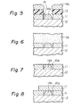
- As illustrated in Figure 5, an insulating layer 11 (e.g. PSG or Si02) is formed on a semiconductor substrate 12 (e.g. a silicon wafer). A
photoresist layer 13 is coated on insulatinglayer 11, is exposed, and is developed to form a photoresist pattern having a through hole.Insulating layer 11 is selectively etched with a suitable etchant through the through hole to form a contact hole (i.e., a through aperture). Then a high-melting point metal, such as molybdenum (Mo), tantalum (Ta), titanium (Ti), tungsten (W), or platinum (Pt), is deposited onphotoresist layer 13 and on the exposed portion ofsemiconductor substrate 12 by a sputtering method to form metal layer 14a andcontact electrode 14b. It is possible to use a silicide of one of the above-mentioned metals (MoSi2 , TaSi , TiSi, WSi2 , and Pt2Si) instead of a high-melting point metal. It is preferable to make the thickness of metal layer 14a equal to that ofinsulating layer 11.Contact electrode 14b is positioned within the contact hole of insulatinglayer 11, andwedge gap 15 is formed betweencontact electrode 14b and the side ofinsulating layer 11. -
Photoresist layer 13 is removed with a suitable solvent, and, therefore, metal layer 14a can be removed. Then, as illustrated in Fig. 6, polycrystalline silicon is deposited on the surfaces ofinsulating layer 11 andcontact electrode 14b by a low-pressure chemical vapour deposition (CVD) method to formpolycrystalline silicon layer 16. In this case, the thermal decomposition of silane (SiH4) or the reduction of SiC14 (or SiH2C12) with hydrogen is carried out at a reaction temperature of from 600°C to 700°C so that it is impossible to use aluminum (Al) forcontact electrode 14b. Moreover, thewedge gap 15 can be completely filled with the polycrystalline silicon. -
Polycrystalline silicon layer 16 is etched to expose the surface of insulatinglayer 11 by a dry etching method, such as a reactive sputter etching method, as illustrated in Fig. 7. If the thickness ofcontact electrode 14b is equal to that ofinsulating layer 11, the surface ofcontact electrode 14b is also exposed. Wedge-shapedpolycrystalline silicon portion 16a remains in the wedge gap so that a substantially level surface of the entire layer comprisinginsulating layer 11,contact electrode 14b, and wedgepolycrystalline silicon portion 16a can be obtained. - Then, as illustrated in Fig. 8, Al is deposited on the level surface (i.e., on the surface of
insulating layer 11, wedgepolycrystalline silicon portion 16a, andcontact electrode 14b) by a vacuum evaporation method to form aconductor layer 17 without causing cracks to form. Conductor (Al)layer 17 is selectively etched by a conventional photoetching method to form a conductor line for interconnection. It is possible to use one of the above-mentioned high-melting point metals, such as Mo, Ta, Ti, W, or Pt, instead of Al. In this case,conductor layer 17 is formed by sputtering the high-melting point metal. The resultant device is heated so as to alloy wedgepolycrystalline silicon portion 16a with the conductor line- and/orcontact electrode 14b. The heating temperature is approximately 400°C to 500°C in the case of the Al conductor line and is from 900°C to 1000°C in the case of the high-melting point melt conductor line. Contactelectrode 14b and the alloy ofpolycrystalline silicon portion 16a ensure an ohmic contact between conductor line andsemiconductor substrate 12. Thus, a semiconductor device having a conductor line free of cracks can be produced. - In the case of the Al conductor line, if a PSG layer is formed on the conductor line and on
insulating layer 11 as a passivation film, the alloying is carried out during the formation of PSG by the CVD method. - It is possible to produce a semiconductor device in accordance with the second embodiment of the present invention. This process of production will now be explained, referring to Figs. 9 and 10. In Fig. 9, a contact hole is formed in insulating
layer 21 lying onsemiconductor substrate 22 in the same manner as that of the first embodiment. The photoresist layer (not shown) on insulatinglayer 21 is removed with a suitable solvent. One of the above-mentioned high-melting point metals is deposited on insulatinglayer 21 and on the exposed portion ofsemiconductor substrate 22 by a sputtering method to formmetal layer 23a andcontact electrode 23b, respectively.Wedge gap 24 is formed betweencontact electrode 23b and the side ofinsulating layer 21. - As illustrated in Fig. 10, polycrystalline silicon is deposited on the surfaces of
metal layer 23a andcontact electrode 23b by a low-pressure CVD method to formpolycrystalline silicon layer 25. The wedge gap is filled withpolycrystalline silicon layer 25. Thenpolycrystalline silicon layer 25 andmetal layer 23a are etched by a dry etching method so as to expose the surface of insulatinglayer 21. Thus, the obtained structure having a level surface is the same as that illustrated in Fig. 7. - A conductor line of Al or of one of the above-mentioned high-melting point metals is formed and then a heat treatment for alloying of the portion of
polycrystalline silicon layer 25 remaining in the wedge gap with the conductor line and/orcontact electrode 23b is carried out in the same manner as that of the first embodiment. As a result, it is possible to produce a semiconductor device having a conductor line free of cracks, the structure of the device being the same as that illustrated in Fig. 8. - It is also possible to produce a semiconductor device in accordance with the third embodiment of the present invention. This process of production will be explained referring to Figs. 11 and 12. In Fig. 11, a contact hole is formed in insulating
layer 31 lying onsemiconductor substrate 32 in the same manner as that of the first embodiment. The photoresist layer (not shown) on insulatinglayer 31 is removed with a suitable solvent. Thinpolycrystalline silicon layer 33 is formed on the exposed surfaces of insulatinglayer 31 andsemiconductor substrate 32 by a low-pressure CVD method. Preferably, thepolycrystalline silicon layer 33 is heavily doped as deposited or by means of thermal impurity diffusion or ion implantation after the deposition. Then one of the above--mentioned high-melting point metals is deposited on thinpolycrystalline silicon layer 33 by a sputtering method so thatmetal layer 34a and contact electrode 34b are formed. Contact electrode 34b is positioned within a blind hole ofthin silicon layer 33, and a wedge gap is formed between contact electrode 34b and the vertical surface ofthin silicon layer 33. For example, the thicknesses of insulatinglayer 31, thinpolycrystalline silicon layer 33, andmetal layer 34a are approximately 800 nm, approximately 100 nm, and from 400 to 700 nm, respectively. Polycrystalline silicon is deposited on the entire exposed surface by a low-pressure CVD method to formpolycrystalline silicon layer 35, with which the wedge gap is filled. - Then, as illustrated in Fig. 12,
polycrystalline silicon layer 35,metal layer 34a, and thinpolycrystalline silicon layer 33 are etched by a dry etching method so as to expose the surface of insulatinglayer 31. Portion 35a ofsilicon layer 35 remains in the wedge gap. - A conductor line (not shown) consisting of a high--melting point metal is formed by using a sputtering method and a photoetching method and then a heat treatment for alloying the polycrystalline silicon of wedge portion 35a and remaining
thin layer 33 with the high-melting point metal of the conductor line and contact electrode 34b is carried out in the same manner as that of the first embodiment. - In a case where a conductor line is made of Al, it is preferable to perform a heat treatment for alloying the polycrystalline silicon of wedge portion 35a and
thin layer 33 with contact electrode 34b prior to the formation of the Al conductor line. The heat-treatment conditions are, for example, a heating temperature of 1000°C and a heating time of ten minutes. After the formation of the Al conductor line, the Al conductor line is subjected to a heat treatment (annealing) at approximately 400°C to 500°C. - Thus, it is possible to produce a semiconductor device having a conductor line free of cracks since the wedge polycrystalline silicon portion ensures the formation of a substantially level surface, as illustrated in Fig. 12.
Claims (7)
Applications Claiming Priority (2)
| Application Number | Priority Date | Filing Date | Title |
|---|---|---|---|
| JP114716/81 | 1981-07-21 | ||
| JP56114716A JPS5815250A (en) | 1981-07-21 | 1981-07-21 | Manufacture of semiconductor device |
Publications (3)
| Publication Number | Publication Date |
|---|---|
| EP0070737A2 true EP0070737A2 (en) | 1983-01-26 |
| EP0070737A3 EP0070737A3 (en) | 1984-06-06 |
| EP0070737B1 EP0070737B1 (en) | 1986-10-01 |
Family
ID=14644827
Family Applications (1)
| Application Number | Title | Priority Date | Filing Date |
|---|---|---|---|
| EP82303828A Expired EP0070737B1 (en) | 1981-07-21 | 1982-07-21 | Semiconductor device having an electrode, and method for producing the same |
Country Status (4)
| Country | Link |
|---|---|
| US (1) | US4801559A (en) |
| EP (1) | EP0070737B1 (en) |
| JP (1) | JPS5815250A (en) |
| DE (1) | DE3273569D1 (en) |
Cited By (8)
| Publication number | Priority date | Publication date | Assignee | Title |
|---|---|---|---|---|
| EP0123309A2 (en) * | 1983-04-25 | 1984-10-31 | Siemens Aktiengesellschaft | Method of producing stable, low ohmic contacts in integrated semiconductor circuits |
| FR2563048A1 (en) * | 1984-04-13 | 1985-10-18 | Efcis | PROCESS FOR MAKING ALUMINUM CONTACTS THROUGH A THICK INSULATING LAYER IN AN INTEGRATED CIRCUIT |
| FR2566181A1 (en) * | 1984-06-14 | 1985-12-20 | Commissariat Energie Atomique | METHOD FOR SELF-POSITIONING OF AN INTERCONNECTION LINE ON AN ELECTRIC CONTACT HOLE OF AN INTEGRATED CIRCUIT |
| EP0211888A1 (en) * | 1985-01-29 | 1987-03-04 | Ramtron Corporation | Method of making an integrated ferroelectric device, and device produced thereby |
| EP0228183A2 (en) * | 1985-11-27 | 1987-07-08 | Kabushiki Kaisha Toshiba | Method for manufacturing semiconductor device |
| EP0561132A1 (en) * | 1992-02-26 | 1993-09-22 | International Business Machines Corporation | Refractory metal capped low resistivity metal conductor lines and vias formed using PVD and CVD |
| US6350676B1 (en) | 1991-11-22 | 2002-02-26 | Sgs-Thomson Microelectronics, S.R.L. | Method of forming high-stability metallic contacts in an integrated circuit with one or more metallized layers |
| WO2010005866A1 (en) * | 2008-07-11 | 2010-01-14 | Sandisk 3D Llc | Method of making a nonvolatile memory device |
Families Citing this family (17)
| Publication number | Priority date | Publication date | Assignee | Title |
|---|---|---|---|---|
| US4961822A (en) * | 1989-04-17 | 1990-10-09 | Liao Kuan Y | Fully recessed interconnection scheme with titanium-tungsten and selective CVD tungsten |
| JP2954263B2 (en) * | 1990-03-22 | 1999-09-27 | 沖電気工業株式会社 | Method for manufacturing semiconductor device |
| US5540810A (en) * | 1992-12-11 | 1996-07-30 | Micron Technology Inc. | IC mechanical planarization process incorporating two slurry compositions for faster material removal times |
| US5950099A (en) * | 1996-04-09 | 1999-09-07 | Kabushiki Kaisha Toshiba | Method of forming an interconnect |
| JP2001118927A (en) * | 1999-10-22 | 2001-04-27 | Mitsubishi Electric Corp | Semiconductor device and manufacturing method therefor |
| US6774488B2 (en) * | 2001-10-22 | 2004-08-10 | Winbond Electronics Corp. | Low leakage and low resistance for memory and the manufacturing method for the plugs |
| CN1301551C (en) * | 2002-12-13 | 2007-02-21 | 华邦电子股份有限公司 | Storage unit manufacturing method and apparatus |
| US7348672B2 (en) * | 2005-07-07 | 2008-03-25 | Taiwan Semiconductor Manufacturing Co., Ltd. | Interconnects with improved reliability |
| US20070052047A1 (en) * | 2005-09-01 | 2007-03-08 | Costas Hadjiloucas | Metal contact systems for semiconductor-based pressure sensors exposed to harsh chemical and thermal environments |
| US20100068275A1 (en) * | 2008-09-16 | 2010-03-18 | Searete Llc, A Limited Liability Corporation Of The State Of Delaware | Personalizable dosage form |
| US20100068283A1 (en) * | 2008-09-16 | 2010-03-18 | Searete Llc, A Limited Liability Corporation Of The State Of Delaware | Ex VIVO modifiable particle or polymeric material medicament carrier |
| US20100069821A1 (en) * | 2008-09-16 | 2010-03-18 | Searete Llc, A Limited Liability Corporation Of The State Of Delaware | Ex vivo modifiable medicament release-sites final dosage form |
| US20100068254A1 (en) * | 2008-09-16 | 2010-03-18 | Mahalaxmi Gita Bangera | Modifying a medicament availability state of a final dosage form |
| US20100068152A1 (en) * | 2008-09-16 | 2010-03-18 | Searete Llc, A Limited Liability Corporation Of The State Of Delaware | Ex vivo modifiable particle or polymeric based final dosage form |
| US20100068235A1 (en) * | 2008-09-16 | 2010-03-18 | Searete LLC, a limited liability corporation of Deleware | Individualizable dosage form |
| US20100068153A1 (en) * | 2008-09-16 | 2010-03-18 | Searete Llc, A Limited Liability Corporation Of The State Of Delaware | Ex vivo activatable final dosage form |
| US20100068233A1 (en) * | 2008-09-16 | 2010-03-18 | Searete Llc, A Limited Liability Corporation Of The State Of Delaware | Modifiable dosage form |
Citations (3)
| Publication number | Priority date | Publication date | Assignee | Title |
|---|---|---|---|---|
| DE1806980A1 (en) * | 1967-11-15 | 1969-06-19 | Fairchild Camera Instr Co | Semiconductor component |
| US4163246A (en) * | 1977-02-07 | 1979-07-31 | Nippon Electric Co., Ltd. | Semiconductor integrated circuit device employing a polycrystalline silicon as a wiring layer |
| US4164461A (en) * | 1977-01-03 | 1979-08-14 | Raytheon Company | Semiconductor integrated circuit structures and manufacturing methods |
Family Cites Families (12)
| Publication number | Priority date | Publication date | Assignee | Title |
|---|---|---|---|---|
| US4017886A (en) * | 1972-10-18 | 1977-04-12 | Hitachi, Ltd. | Discrete semiconductor device having polymer resin as insulator and method for making the same |
| US3946476A (en) * | 1975-01-22 | 1976-03-30 | Dracon Industries | Automatic multi-conductor quick connect termination tool |
| JPS522166A (en) * | 1975-06-24 | 1977-01-08 | Hitachi Ltd | Method of pulling out wiring from highly inpure dope layer |
| JPS5228868A (en) * | 1975-08-29 | 1977-03-04 | Hitachi Ltd | Semiconductor device |
| US4045594A (en) * | 1975-12-31 | 1977-08-30 | Ibm Corporation | Planar insulation of conductive patterns by chemical vapor deposition and sputtering |
| JPS52106675A (en) * | 1976-03-05 | 1977-09-07 | Toshiba Corp | Manufacturing method of semiconductor device |
| JPS5317393A (en) * | 1976-07-31 | 1978-02-17 | Mitsubishi Heavy Ind Ltd | Commodities delivery detector |
| US4109372A (en) * | 1977-05-02 | 1978-08-29 | International Business Machines Corporation | Method for making an insulated gate field effect transistor utilizing a silicon gate and silicide interconnection vias |
| JPS543480A (en) * | 1977-06-09 | 1979-01-11 | Fujitsu Ltd | Manufacture of semiconductor device |
| JPS5585042A (en) * | 1978-12-21 | 1980-06-26 | Mitsubishi Electric Corp | Semiconductor device |
| US4291322A (en) * | 1979-07-30 | 1981-09-22 | Bell Telephone Laboratories, Incorporated | Structure for shallow junction MOS circuits |
| JPS5932151A (en) * | 1982-08-18 | 1984-02-21 | Nippon Telegr & Teleph Corp <Ntt> | Manufacture of semiconductor device |
-
1981
- 1981-07-21 JP JP56114716A patent/JPS5815250A/en active Granted
-
1982
- 1982-07-21 DE DE8282303828T patent/DE3273569D1/en not_active Expired
- 1982-07-21 EP EP82303828A patent/EP0070737B1/en not_active Expired
-
1988
- 1988-02-29 US US07/165,367 patent/US4801559A/en not_active Expired - Fee Related
Patent Citations (3)
| Publication number | Priority date | Publication date | Assignee | Title |
|---|---|---|---|---|
| DE1806980A1 (en) * | 1967-11-15 | 1969-06-19 | Fairchild Camera Instr Co | Semiconductor component |
| US4164461A (en) * | 1977-01-03 | 1979-08-14 | Raytheon Company | Semiconductor integrated circuit structures and manufacturing methods |
| US4163246A (en) * | 1977-02-07 | 1979-07-31 | Nippon Electric Co., Ltd. | Semiconductor integrated circuit device employing a polycrystalline silicon as a wiring layer |
Non-Patent Citations (1)
| Title |
|---|
| IBM TECHNICAL DISCLOSURE BULLETIN, vol. 21, no. 3, August 1978, pages 1052-1053, New York, US; J. GNIEWEK et al.: "Dual insulators for planar multilevel interconnections". * |
Cited By (20)
| Publication number | Priority date | Publication date | Assignee | Title |
|---|---|---|---|---|
| EP0123309A2 (en) * | 1983-04-25 | 1984-10-31 | Siemens Aktiengesellschaft | Method of producing stable, low ohmic contacts in integrated semiconductor circuits |
| EP0123309A3 (en) * | 1983-04-25 | 1987-09-30 | Siemens Aktiengesellschaft Berlin Und Munchen | Method of producing stable, low ohmic contacts in integrated semiconductor circuits |
| FR2563048A1 (en) * | 1984-04-13 | 1985-10-18 | Efcis | PROCESS FOR MAKING ALUMINUM CONTACTS THROUGH A THICK INSULATING LAYER IN AN INTEGRATED CIRCUIT |
| EP0165085A1 (en) * | 1984-04-13 | 1985-12-18 | STMicroelectronics S.A. | Method of manufacturing aluminium contacts through a thick insulating layer in a circuit |
| FR2566181A1 (en) * | 1984-06-14 | 1985-12-20 | Commissariat Energie Atomique | METHOD FOR SELF-POSITIONING OF AN INTERCONNECTION LINE ON AN ELECTRIC CONTACT HOLE OF AN INTEGRATED CIRCUIT |
| EP0170544A1 (en) * | 1984-06-14 | 1986-02-05 | Commissariat A L'energie Atomique | Self-aligning method of forming an interconnection line over a contact hole in an integrated circuit |
| US4624864A (en) * | 1984-06-14 | 1986-11-25 | Commissariat A L'energie Atomique | Process for the autopositioning of an interconnection line on an electric contact hole of an integrated circuit |
| EP0211888A4 (en) * | 1985-01-29 | 1988-08-04 | Ramtron Corp | Method of making an integrated ferroelectric device, and device produced thereby. |
| EP0211888A1 (en) * | 1985-01-29 | 1987-03-04 | Ramtron Corporation | Method of making an integrated ferroelectric device, and device produced thereby |
| EP0228183A3 (en) * | 1985-11-27 | 1989-10-18 | Kabushiki Kaisha Toshiba | Method for manufacturing semiconductor device |
| EP0228183A2 (en) * | 1985-11-27 | 1987-07-08 | Kabushiki Kaisha Toshiba | Method for manufacturing semiconductor device |
| US6350676B1 (en) | 1991-11-22 | 2002-02-26 | Sgs-Thomson Microelectronics, S.R.L. | Method of forming high-stability metallic contacts in an integrated circuit with one or more metallized layers |
| EP0561132A1 (en) * | 1992-02-26 | 1993-09-22 | International Business Machines Corporation | Refractory metal capped low resistivity metal conductor lines and vias formed using PVD and CVD |
| EP0788156A2 (en) * | 1992-02-26 | 1997-08-06 | International Business Machines Corporation | Refractory metal capped low resistivity metal conductor lines and vias formed using PVD and CVD |
| EP0788156A3 (en) * | 1992-02-26 | 1998-04-15 | International Business Machines Corporation | Refractory metal capped low resistivity metal conductor lines and vias formed using PVD and CVD |
| US5889328A (en) * | 1992-02-26 | 1999-03-30 | International Business Machines Corporation | Refractory metal capped low resistivity metal conductor lines and vias |
| US5976975A (en) * | 1992-02-26 | 1999-11-02 | International Business Machines Corporation | Refractory metal capped low resistivity metal conductor lines and vias |
| US6147402A (en) * | 1992-02-26 | 2000-11-14 | International Business Machines Corporation | Refractory metal capped low resistivity metal conductor lines and vias |
| US6323554B1 (en) | 1992-02-26 | 2001-11-27 | International Business Machines Corporation | Refractory metal capped low resistivity metal conductor lines and vias formed using PVD and CVD |
| WO2010005866A1 (en) * | 2008-07-11 | 2010-01-14 | Sandisk 3D Llc | Method of making a nonvolatile memory device |
Also Published As
| Publication number | Publication date |
|---|---|
| JPS5815250A (en) | 1983-01-28 |
| JPS637464B2 (en) | 1988-02-17 |
| US4801559A (en) | 1989-01-31 |
| EP0070737A3 (en) | 1984-06-06 |
| EP0070737B1 (en) | 1986-10-01 |
| DE3273569D1 (en) | 1986-11-06 |
Similar Documents
| Publication | Publication Date | Title |
|---|---|---|
| EP0070737B1 (en) | Semiconductor device having an electrode, and method for producing the same | |
| KR910002455B1 (en) | Semiconductor device | |
| EP0499433B1 (en) | Semiconductor device with improved reliability wiring and method of its fabrication | |
| KR0179822B1 (en) | Interconnections structure of semiconductor device and method for manufacturing thereof | |
| US5183782A (en) | Process for fabricating a semiconductor device including a tungsten silicide adhesive layer | |
| US4708904A (en) | Semiconductor device and a method of manufacturing the same | |
| US4589196A (en) | Contacts for VLSI devices using direct-reacted silicide | |
| US5414404A (en) | Semiconductor device having a thin-film resistor | |
| US3856648A (en) | Method of forming contact and interconnect geometries for semiconductor devices and integrated circuits | |
| JPS63133648A (en) | Tungsten covering | |
| EP0147247A2 (en) | Method for forming hillock suppression layer in dual metal layer processing and structure formed thereby | |
| JPS60182133A (en) | Manufacture of semiconductor device | |
| JP2798250B2 (en) | Method of forming low resistance contact with aluminum material and low resistance contact with aluminum | |
| US4890151A (en) | Thin-film and its forming method | |
| KR0139599B1 (en) | Mechod of forming metal wiring in semiconducotr device | |
| KR100191710B1 (en) | Metal wiring method of semiconductor device | |
| US5663094A (en) | Process for producing semiconductor device with wire for three conductive layers | |
| JPS5961147A (en) | Manufacture of semiconductor device | |
| KR100373364B1 (en) | Method for forming metal line | |
| KR100186985B1 (en) | Manufacture of semiconductor device | |
| KR100369352B1 (en) | Semiconductor device and manufacturing method thereof | |
| JPH04247625A (en) | Wiring formation | |
| JP3328459B2 (en) | Method for manufacturing semiconductor device | |
| JPS59163822A (en) | Manufacture of semiconductor device | |
| EP0543254A2 (en) | A method of forming high-stability metallic contacts in an integrated circuit with one or more metallized layers |
Legal Events
| Date | Code | Title | Description |
|---|---|---|---|
| PUAI | Public reference made under article 153(3) epc to a published international application that has entered the european phase |
Free format text: ORIGINAL CODE: 0009012 |
|
| AK | Designated contracting states |
Designated state(s): DE FR GB |
|
| PUAL | Search report despatched |
Free format text: ORIGINAL CODE: 0009013 |
|
| AK | Designated contracting states |
Designated state(s): DE FR GB |
|
| 17P | Request for examination filed |
Effective date: 19840822 |
|
| GRAA | (expected) grant |
Free format text: ORIGINAL CODE: 0009210 |
|
| AK | Designated contracting states |
Kind code of ref document: B1 Designated state(s): DE FR GB |
|
| REF | Corresponds to: |
Ref document number: 3273569 Country of ref document: DE Date of ref document: 19861106 |
|
| ET | Fr: translation filed | ||
| PLBE | No opposition filed within time limit |
Free format text: ORIGINAL CODE: 0009261 |
|
| STAA | Information on the status of an ep patent application or granted ep patent |
Free format text: STATUS: NO OPPOSITION FILED WITHIN TIME LIMIT |
|
| 26N | No opposition filed | ||
| PGFP | Annual fee paid to national office [announced via postgrant information from national office to epo] |
Ref country code: GB Payment date: 19920713 Year of fee payment: 11 |
|
| PGFP | Annual fee paid to national office [announced via postgrant information from national office to epo] |
Ref country code: FR Payment date: 19920730 Year of fee payment: 11 |
|
| PGFP | Annual fee paid to national office [announced via postgrant information from national office to epo] |
Ref country code: DE Payment date: 19920922 Year of fee payment: 11 |
|
| PG25 | Lapsed in a contracting state [announced via postgrant information from national office to epo] |
Ref country code: GB Effective date: 19930721 |
|
| GBPC | Gb: european patent ceased through non-payment of renewal fee |
Effective date: 19930721 |
|
| PG25 | Lapsed in a contracting state [announced via postgrant information from national office to epo] |
Ref country code: FR Effective date: 19940331 |
|
| PG25 | Lapsed in a contracting state [announced via postgrant information from national office to epo] |
Ref country code: DE Effective date: 19940401 |
|
| REG | Reference to a national code |
Ref country code: FR Ref legal event code: ST |