EP0072216A2 - The production of semiconductor devices by methods involving annealing - Google Patents
The production of semiconductor devices by methods involving annealing Download PDFInfo
- Publication number
- EP0072216A2 EP0072216A2 EP82304148A EP82304148A EP0072216A2 EP 0072216 A2 EP0072216 A2 EP 0072216A2 EP 82304148 A EP82304148 A EP 82304148A EP 82304148 A EP82304148 A EP 82304148A EP 0072216 A2 EP0072216 A2 EP 0072216A2
- Authority
- EP
- European Patent Office
- Prior art keywords
- aluminum
- insulating layer
- electrode
- gate electrode
- annealing
- Prior art date
- Legal status (The legal status is an assumption and is not a legal conclusion. Google has not performed a legal analysis and makes no representation as to the accuracy of the status listed.)
- Granted
Links
- 238000000034 method Methods 0.000 title claims abstract description 40
- 239000004065 semiconductor Substances 0.000 title claims abstract description 26
- 238000000137 annealing Methods 0.000 title claims abstract description 15
- 238000004519 manufacturing process Methods 0.000 title description 5
- XAGFODPZIPBFFR-UHFFFAOYSA-N aluminium Chemical compound [Al] XAGFODPZIPBFFR-UHFFFAOYSA-N 0.000 claims abstract description 52
- 229910052782 aluminium Inorganic materials 0.000 claims abstract description 52
- 239000012535 impurity Substances 0.000 claims abstract description 19
- 239000000758 substrate Substances 0.000 claims abstract description 16
- 150000002500 ions Chemical class 0.000 claims abstract description 6
- 230000001678 irradiating effect Effects 0.000 claims abstract description 3
- 238000002513 implantation Methods 0.000 claims abstract 2
- VYPSYNLAJGMNEJ-UHFFFAOYSA-N Silicium dioxide Chemical compound O=[Si]=O VYPSYNLAJGMNEJ-UHFFFAOYSA-N 0.000 claims description 10
- TWNQGVIAIRXVLR-UHFFFAOYSA-N oxo(oxoalumanyloxy)alumane Chemical compound O=[Al]O[Al]=O TWNQGVIAIRXVLR-UHFFFAOYSA-N 0.000 claims description 9
- 235000012239 silicon dioxide Nutrition 0.000 claims description 5
- 239000000377 silicon dioxide Substances 0.000 claims description 5
- 229910052581 Si3N4 Inorganic materials 0.000 claims description 2
- 238000010894 electron beam technology Methods 0.000 claims description 2
- 238000005468 ion implantation Methods 0.000 claims description 2
- HQVNEWCFYHHQES-UHFFFAOYSA-N silicon nitride Chemical compound N12[Si]34N5[Si]62N3[Si]51N64 HQVNEWCFYHHQES-UHFFFAOYSA-N 0.000 claims description 2
- 230000005855 radiation Effects 0.000 claims 1
- 238000010521 absorption reaction Methods 0.000 description 6
- 239000000463 material Substances 0.000 description 6
- 230000000873 masking effect Effects 0.000 description 5
- 230000003647 oxidation Effects 0.000 description 5
- 238000007254 oxidation reaction Methods 0.000 description 5
- 239000005360 phosphosilicate glass Substances 0.000 description 5
- XUIMIQQOPSSXEZ-UHFFFAOYSA-N Silicon Chemical compound [Si] XUIMIQQOPSSXEZ-UHFFFAOYSA-N 0.000 description 3
- 230000015572 biosynthetic process Effects 0.000 description 3
- 230000010354 integration Effects 0.000 description 3
- 239000010979 ruby Substances 0.000 description 3
- 229910001750 ruby Inorganic materials 0.000 description 3
- 229910052710 silicon Inorganic materials 0.000 description 3
- 239000010703 silicon Substances 0.000 description 3
- 229910052785 arsenic Inorganic materials 0.000 description 2
- -1 arsenic ions Chemical class 0.000 description 2
- 238000005336 cracking Methods 0.000 description 2
- 239000006185 dispersion Substances 0.000 description 2
- 238000005224 laser annealing Methods 0.000 description 2
- 238000000059 patterning Methods 0.000 description 2
- 238000005229 chemical vapour deposition Methods 0.000 description 1
- 238000001816 cooling Methods 0.000 description 1
- 230000001627 detrimental effect Effects 0.000 description 1
- 238000009826 distribution Methods 0.000 description 1
- 230000000694 effects Effects 0.000 description 1
- 230000005669 field effect Effects 0.000 description 1
- 238000010438 heat treatment Methods 0.000 description 1
- 238000012986 modification Methods 0.000 description 1
- 230000004048 modification Effects 0.000 description 1
- 229910021420 polycrystalline silicon Inorganic materials 0.000 description 1
Images

Classifications
-
- H—ELECTRICITY
- H01—ELECTRIC ELEMENTS
- H01L—SEMICONDUCTOR DEVICES NOT COVERED BY CLASS H10
- H01L21/00—Processes or apparatus adapted for the manufacture or treatment of semiconductor or solid state devices or of parts thereof
- H01L21/02—Manufacture or treatment of semiconductor devices or of parts thereof
- H01L21/04—Manufacture or treatment of semiconductor devices or of parts thereof the devices having at least one potential-jump barrier or surface barrier, e.g. PN junction, depletion layer or carrier concentration layer
- H01L21/18—Manufacture or treatment of semiconductor devices or of parts thereof the devices having at least one potential-jump barrier or surface barrier, e.g. PN junction, depletion layer or carrier concentration layer the devices having semiconductor bodies comprising elements of Group IV of the Periodic System or AIIIBV compounds with or without impurities, e.g. doping materials
- H01L21/28—Manufacture of electrodes on semiconductor bodies using processes or apparatus not provided for in groups H01L21/20 - H01L21/268
- H01L21/28008—Making conductor-insulator-semiconductor electrodes
-
- H—ELECTRICITY
- H01—ELECTRIC ELEMENTS
- H01L—SEMICONDUCTOR DEVICES NOT COVERED BY CLASS H10
- H01L21/00—Processes or apparatus adapted for the manufacture or treatment of semiconductor or solid state devices or of parts thereof
- H01L21/02—Manufacture or treatment of semiconductor devices or of parts thereof
- H01L21/04—Manufacture or treatment of semiconductor devices or of parts thereof the devices having at least one potential-jump barrier or surface barrier, e.g. PN junction, depletion layer or carrier concentration layer
- H01L21/18—Manufacture or treatment of semiconductor devices or of parts thereof the devices having at least one potential-jump barrier or surface barrier, e.g. PN junction, depletion layer or carrier concentration layer the devices having semiconductor bodies comprising elements of Group IV of the Periodic System or AIIIBV compounds with or without impurities, e.g. doping materials
- H01L21/26—Bombardment with radiation
- H01L21/263—Bombardment with radiation with high-energy radiation
- H01L21/2636—Bombardment with radiation with high-energy radiation for heating, e.g. electron beam heating
-
- H—ELECTRICITY
- H01—ELECTRIC ELEMENTS
- H01L—SEMICONDUCTOR DEVICES NOT COVERED BY CLASS H10
- H01L21/00—Processes or apparatus adapted for the manufacture or treatment of semiconductor or solid state devices or of parts thereof
- H01L21/02—Manufacture or treatment of semiconductor devices or of parts thereof
- H01L21/04—Manufacture or treatment of semiconductor devices or of parts thereof the devices having at least one potential-jump barrier or surface barrier, e.g. PN junction, depletion layer or carrier concentration layer
- H01L21/18—Manufacture or treatment of semiconductor devices or of parts thereof the devices having at least one potential-jump barrier or surface barrier, e.g. PN junction, depletion layer or carrier concentration layer the devices having semiconductor bodies comprising elements of Group IV of the Periodic System or AIIIBV compounds with or without impurities, e.g. doping materials
- H01L21/26—Bombardment with radiation
- H01L21/263—Bombardment with radiation with high-energy radiation
- H01L21/268—Bombardment with radiation with high-energy radiation using electromagnetic radiation, e.g. laser radiation
-
- H—ELECTRICITY
- H01—ELECTRIC ELEMENTS
- H01L—SEMICONDUCTOR DEVICES NOT COVERED BY CLASS H10
- H01L29/00—Semiconductor devices adapted for rectifying, amplifying, oscillating or switching, or capacitors or resistors with at least one potential-jump barrier or surface barrier, e.g. PN junction depletion layer or carrier concentration layer; Details of semiconductor bodies or of electrodes thereof ; Multistep manufacturing processes therefor
- H01L29/66—Types of semiconductor device ; Multistep manufacturing processes therefor
- H01L29/66007—Multistep manufacturing processes
- H01L29/66075—Multistep manufacturing processes of devices having semiconductor bodies comprising group 14 or group 13/15 materials
- H01L29/66227—Multistep manufacturing processes of devices having semiconductor bodies comprising group 14 or group 13/15 materials the devices being controllable only by the electric current supplied or the electric potential applied, to an electrode which does not carry the current to be rectified, amplified or switched, e.g. three-terminal devices
- H01L29/66409—Unipolar field-effect transistors
- H01L29/66477—Unipolar field-effect transistors with an insulated gate, i.e. MISFET
- H01L29/66568—Lateral single gate silicon transistors
- H01L29/66575—Lateral single gate silicon transistors where the source and drain or source and drain extensions are self-aligned to the sides of the gate
-
- H—ELECTRICITY
- H01—ELECTRIC ELEMENTS
- H01L—SEMICONDUCTOR DEVICES NOT COVERED BY CLASS H10
- H01L29/00—Semiconductor devices adapted for rectifying, amplifying, oscillating or switching, or capacitors or resistors with at least one potential-jump barrier or surface barrier, e.g. PN junction depletion layer or carrier concentration layer; Details of semiconductor bodies or of electrodes thereof ; Multistep manufacturing processes therefor
- H01L29/66—Types of semiconductor device ; Multistep manufacturing processes therefor
- H01L29/68—Types of semiconductor device ; Multistep manufacturing processes therefor controllable by only the electric current supplied, or only the electric potential applied, to an electrode which does not carry the current to be rectified, amplified or switched
- H01L29/76—Unipolar devices, e.g. field effect transistors
- H01L29/772—Field effect transistors
- H01L29/78—Field effect transistors with field effect produced by an insulated gate
-
- Y—GENERAL TAGGING OF NEW TECHNOLOGICAL DEVELOPMENTS; GENERAL TAGGING OF CROSS-SECTIONAL TECHNOLOGIES SPANNING OVER SEVERAL SECTIONS OF THE IPC; TECHNICAL SUBJECTS COVERED BY FORMER USPC CROSS-REFERENCE ART COLLECTIONS [XRACs] AND DIGESTS
- Y10—TECHNICAL SUBJECTS COVERED BY FORMER USPC
- Y10S—TECHNICAL SUBJECTS COVERED BY FORMER USPC CROSS-REFERENCE ART COLLECTIONS [XRACs] AND DIGESTS
- Y10S148/00—Metal treatment
- Y10S148/09—Laser anneal
-
- Y—GENERAL TAGGING OF NEW TECHNOLOGICAL DEVELOPMENTS; GENERAL TAGGING OF CROSS-SECTIONAL TECHNOLOGIES SPANNING OVER SEVERAL SECTIONS OF THE IPC; TECHNICAL SUBJECTS COVERED BY FORMER USPC CROSS-REFERENCE ART COLLECTIONS [XRACs] AND DIGESTS
- Y10—TECHNICAL SUBJECTS COVERED BY FORMER USPC
- Y10S—TECHNICAL SUBJECTS COVERED BY FORMER USPC CROSS-REFERENCE ART COLLECTIONS [XRACs] AND DIGESTS
- Y10S148/00—Metal treatment
- Y10S148/091—Laser beam processing of fets
-
- Y—GENERAL TAGGING OF NEW TECHNOLOGICAL DEVELOPMENTS; GENERAL TAGGING OF CROSS-SECTIONAL TECHNOLOGIES SPANNING OVER SEVERAL SECTIONS OF THE IPC; TECHNICAL SUBJECTS COVERED BY FORMER USPC CROSS-REFERENCE ART COLLECTIONS [XRACs] AND DIGESTS
- Y10—TECHNICAL SUBJECTS COVERED BY FORMER USPC
- Y10S—TECHNICAL SUBJECTS COVERED BY FORMER USPC CROSS-REFERENCE ART COLLECTIONS [XRACs] AND DIGESTS
- Y10S148/00—Metal treatment
- Y10S148/106—Masks, special
-
- Y—GENERAL TAGGING OF NEW TECHNOLOGICAL DEVELOPMENTS; GENERAL TAGGING OF CROSS-SECTIONAL TECHNOLOGIES SPANNING OVER SEVERAL SECTIONS OF THE IPC; TECHNICAL SUBJECTS COVERED BY FORMER USPC CROSS-REFERENCE ART COLLECTIONS [XRACs] AND DIGESTS
- Y10—TECHNICAL SUBJECTS COVERED BY FORMER USPC
- Y10S—TECHNICAL SUBJECTS COVERED BY FORMER USPC CROSS-REFERENCE ART COLLECTIONS [XRACs] AND DIGESTS
- Y10S148/00—Metal treatment
- Y10S148/141—Self-alignment coat gate
Landscapes
- Engineering & Computer Science (AREA)
- Physics & Mathematics (AREA)
- Power Engineering (AREA)
- Microelectronics & Electronic Packaging (AREA)
- Computer Hardware Design (AREA)
- General Physics & Mathematics (AREA)
- Condensed Matter Physics & Semiconductors (AREA)
- High Energy & Nuclear Physics (AREA)
- Manufacturing & Machinery (AREA)
- Ceramic Engineering (AREA)
- Health & Medical Sciences (AREA)
- Toxicology (AREA)
- Electromagnetism (AREA)
- Optics & Photonics (AREA)
- Insulated Gate Type Field-Effect Transistor (AREA)
- Electrodes Of Semiconductors (AREA)
- Thin Film Transistor (AREA)
- Internal Circuitry In Semiconductor Integrated Circuit Devices (AREA)
Abstract
Description
- The present invention relates to the production of semiconductor devices by methods involving annealing.
- Impurity doped regions in a semiconductor substrate can be formedby using a "self-alignment" method wherein an aluminum gate electrode is used as a mask. Such self alignment methods can be applied to the formation of source and drain regions of field effect transistors (FET) in semiconductor substrates. Since no space is necessary for position alignment of photo masking material in a self--alignment method, self-alignment can be an effective technique to increase the degree of semiconductor device integration. In one such method, however,after gate electrodes are formed on gate insulating layers, heat treatment is carried out at 500°C to activate the source and drain regions using the gate electrodes as masking material. Therefore, in such a self-alignment method, it is necessary that the material of the gate electrodes have high heat resistance. For example, polycrystalline silicon, which has high heat resistance, can be used for the gate electrodes. Even considerable doping of impurities into the polycrystalline, however, fails to reduce the electrical resistance of the doped polycrystalline to the level of aluminum. Thus, the switching speed of such a semiconductor device is lowered, as compared to one having aluminum gate electrodes.
- It is now possible for laser annealing of semiconductors to be employed to activate the source and drain regions. While aluminum has poor heat resistance, it reflects a laser beam well. Therefore, it should be possible to use aluminum for the masking material to form the source and drain regions by the ion-implanting or doping method, then anneal the regions by laser irradiation so as to produce FET's having aluminum gate electrodes by a self-alignment process. As a result, the integration density and switching speed of semiconductor devices can be improved. Japanese Unexamined Patent Publication No. 55-102271 describes the use of aluminum as gate electrodes and annealing an ion--doped layer by laser beam irradiation using the aluminum gate electrodes as masking material. However, in the process described in Japanese Unexamined Patent Publication No. 55-102271, the laser beam irradiation has a detrimental effect on the aluminum gate electrodes. Namely, the effect of irradiation energy of the laser beam on the aluminum is so strong that it damages the aluminum despite much of it being reflected by the aluminum. Irradiation of 2.2 joules of energy by a ruby laser beam, for example, can fuse and further disperse the aluminum of gate electrodes. Irradiation of even 0.31 joules of energy by a laser beam can produce crack network at the surface of the aluminum gate electrodes. Such irradiation energy can thus. damage. the aluminum gate electrodes themselves.
- On the other hand, while irradiation of a low amount of energy by a laser beam, for example 0.146 joules,will not damage the aluminum, it will also not activate the impurity doped regions enough to lower the sheet (surface) resistivity. Thus a region into which arsenic ions(As+)were doped under conditions of 5 x 10 15 cm-2 dose and 100 KeV energy can be reduced only to a sheet resistivity of 100 Ω/□ by an irradiation energy of 0.146 joule compared with a sheet resistivity of 50 Ω/□ by an irradiation energy of 0.3 joule.
- As explained above, a high irradiation energy of a laser beam on aluminum gate electrodes can damage the aluminum, and a low irradiation energy of a laser beam on aluminum gate electrodes may not be sufficient to activate the impurity doped region to lower the sheet resistivity.
- It is desirable to provide : a method for producing a semiconductor device having an aluminum gate electrode in which a low sheet resistivity can be obtained by means of beam annealing at the ion doped region without damage to the aluminum electrode, whereby high integration density and high switching speed can be obtained.
- An embodiment of the present invention provides a method for producing a semiconductor device comprising the steps of:
- forming a gate insulating layer on one conductive type semiconductor substrate;
- forming an aluminum gate electrode on said gate insulating layer;
- forming an impurity doped region in said one conductive type semiconductor substrate by means of doping of opposite conductive type impurity into said one conductive type semiconductor substrate using said aluminum gate electrode as a masking material;
- covering at least the upper face of said aluminum gate electrode with an insulating layer; and
- annealing said impurity doped regions by irradiating a laser beam on said impurity doped regions including said aluminum gate electrode.
- Reeference will now be made, by way of example, . to the accompanying drawings; in which:
- Figs. 1 to 3 are explanatory sectional views illustrating a portion of a semiconductor device being produced by a method embodying the present invention; and
- Fig. 4 is a graph illustrating the relation between laser beam absorption ratio and thickness of an insulating layer.
- Before the present invention was conceived, various studies were carried out,whereby it was found that the reason for the above-described crack network was that when an aluminum gate electrode was heated by beam irradiation, it expanded. During the process of cooling by heat dispersion from the surface, however, the surface would contract first. In a method embodying the present invention it is found that formation of an insulating layer on an aluminum gate electrode before the laser annealing can allow sufficient annealing of the impurity doped region and the aluminum gate electrode and stop formation of crack network. This is because the insulating layer suppresses heat dispersion from the surface of the aluminum gate electrode and results in an even temperature distribution in the aluminum gate electrode. At the same time, the insulating layer can dynamically inhibit the aluminum gate electrode from cracking.
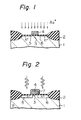
- Referring to Fig. 1, for example, a usual technique is used to form, on p type silicon semiconductor substrate 1, silicon dioxide
field insulating layer 2, silicon dioxidegate insulating layer 3, andaluminum gate electrode 4. - An ion implantation technique is then used to dope arsenic ions into p type silicon substrate 1 at a 5 x 10 15 cm-2 dose amount and 100 KeV energy so as to form n+
type source region 5 and n+ type drain region 6 : in silicon substrate 1. - Referring to Fig. 2, aluminum oxide layer 7 is formed on the surface of the
aluminum gate electrode 4 by oxidation, for example utilizing the anode oxidation process. This oxidation process of aluminum may be carried out prior to the ion implanting process. Then, a YAG laser beam having wavelength of 1.06 µm is irradiated onothe impurity doped regions' and the aluminum gate electrode toanneal source region 5 anddrain region 6, producing a sheet resistivity ofregions aluminum gate electrode 4. - Referring to Fig. 3, a well known technique is used to form phosphosilicate glass layer 8 on the device shown in Fig. 2. An electrode contact hole is formed by patterning phosphosilicate glass layer 8 and silicon dioxide
gate insulating layer 3. As aluminum layer is formed in the electrode contact hole and on phosphosilicate glass layer 8. Source electrode 9 anddrain electrode 10 are formed by patterning the aluminum layer. Phosphosilicate glass layer 11 is formed on source electrode 9, phosphosilicate glass layer 8, anddrain electrode 10 and, thus, an integrated circuit (IC) chip is produced. A further contact hole may also be made to provide for electrical connection to the electrode. The aluminum oxide layer 7 may be changed to another insulating layer, for example, a silicon nitride layer or a silicon dioxide layer. Further, in addition to the anode oxidation process mentioned above, a plasma oxidation process, chemical vapor deposition process (CVD process) and so forth may be used to form aluminum oxide layer 7. - The change in the laser beam absorption ratio of the aluminum layer as a function of the thickness of the insulating layer, in the case where an insulating layer is present on the aluminum layer, is shown in Fig.4. This change is due to the interference of light.
- As apparent from Fig.4, it is effective that thickness t of the insulating layer is equal to the value λm/2n; wherein n is the index of refraction of the insulating layer on the aluminum layer, λ is the beam wavelength in a vacuum, and m is a positive integer. The data shown in Fig.4 was obtained by using a YAG laser having a wavelength of 1.06µm.
- Therefore, in the case of a ruby laser beam having a wavelength of 0.694pm, to minimize the absorption ratio when using aluminum oxide, which has an index of refraction of 1.77, the thickness of the aluminum oxide layer should be 1960 Å. In the case of a YAG laser beam having a wavelength of 1.03pm, to minimize the absorption rate when using aluminum oxide, the thickness of the aluminum oxide layer should be 2900 A. The above thicknesses of the aluminum oxide layers can be calculated from the formula, λm/2n.
- As can be seen from Fig.4, a thickness of λ/12n, considerably lower than λ/4n, can also produce a roughly minimum absorption rate T. On the other hand, to activate the source and drain regions under a gate insulating layer, a large absorption ratio is preferable. Therefore, the thickness of the gate insulating layer should be formed to be λ(2M-1) /4n'; wherein n' is the index of refraction of the gate insulating layer, λ is a beam wavelength in a vacuum, and M is a positive integer.
- In the above examples, a laser beam, in particular a ruby laser beam or YAG laser beam, was used as the beam by which impurity doped regions were annealed. However, in addition to a laser,an electron beam, lamp beam, and so forth may be used.
- In an embodiment of the present invention, as explained above, at least the upper surface of the aluminum gate electrode is covered with an insulating layer of a thickness selected by the formula λm/2n so that the aluminum gate electrode can withstand the annealing, process whereby the source and drain regions are activated, with the result that a low sheet resistivity can be obtained.
- An embodiment of the present invention can thus be used for the production of a semiconductor device including an FET produced by the self-alignment method and using an aluminum gate electrode.
- While preferred embodiments of the invention have been shown, it will be obvious that modifications may be made within the scope of the disclosure of the specification.
Claims (8)
Applications Claiming Priority (2)
| Application Number | Priority Date | Filing Date | Title |
|---|---|---|---|
| JP122657/81 | 1981-08-05 | ||
| JP56122657A JPS5823479A (en) | 1981-08-05 | 1981-08-05 | Manufacture of semiconductor device |
Publications (3)
| Publication Number | Publication Date |
|---|---|
| EP0072216A2 true EP0072216A2 (en) | 1983-02-16 |
| EP0072216A3 EP0072216A3 (en) | 1985-12-18 |
| EP0072216B1 EP0072216B1 (en) | 1989-04-12 |
Family
ID=14841395
Family Applications (1)
| Application Number | Title | Priority Date | Filing Date |
|---|---|---|---|
| EP82304148A Expired EP0072216B1 (en) | 1981-08-05 | 1982-08-05 | The production of semiconductor devices by methods involving annealing |
Country Status (4)
| Country | Link |
|---|---|
| US (1) | US4468855A (en) |
| EP (1) | EP0072216B1 (en) |
| JP (1) | JPS5823479A (en) |
| DE (1) | DE3279614D1 (en) |
Cited By (13)
| Publication number | Priority date | Publication date | Assignee | Title |
|---|---|---|---|---|
| DE3342773A1 (en) * | 1983-11-25 | 1985-06-05 | Siemens AG, 1000 Berlin und 8000 München | Process for producing MOS field-effect transistors with high dielectric strength and with a gentle concentration profile at the drain junction |
| US5308998A (en) * | 1991-08-26 | 1994-05-03 | Semiconductor Energy Laboratory Co., Ltd. | Insulated gate field effect semiconductor devices having a LDD region and an anodic oxide film of a gate electrode |
| US5401666A (en) * | 1992-06-17 | 1995-03-28 | Sony Corporation | Method for selective annealing of a semiconductor device |
| US5650338A (en) * | 1991-08-26 | 1997-07-22 | Semiconductor Energy Laboratory Co., Ltd. | Method for forming thin film transistor |
| USRE36314E (en) * | 1991-03-06 | 1999-09-28 | Semiconductor Energy Laboratory Co., Ltd. | Insulated gate field effect semiconductor devices having a LDD region and an anodic oxide film of a gate electrode |
| US6147375A (en) * | 1992-02-05 | 2000-11-14 | Semiconductor Energy Laboratory Co., Ltd. | Active matrix display device |
| US6323528B1 (en) | 1991-03-06 | 2001-11-27 | Semiconductor Energy Laboratory Co,. Ltd. | Semiconductor device |
| US6410374B1 (en) | 1992-12-26 | 2002-06-25 | Semiconductor Energy Laborartory Co., Ltd. | Method of crystallizing a semiconductor layer in a MIS transistor |
| US6489632B1 (en) | 1993-01-18 | 2002-12-03 | Semiconductor Energy Laboratory Co., Ltd. | Semiconductor device having a gate oxide film |
| US6544825B1 (en) | 1992-12-26 | 2003-04-08 | Semiconductor Energy Laboratory Co., Ltd. | Method of fabricating a MIS transistor |
| US6555843B1 (en) | 1991-05-16 | 2003-04-29 | Semiconductor Energy Laboratory Co., Ltd. | Semiconductor device and method for forming the same |
| US6867431B2 (en) | 1993-09-20 | 2005-03-15 | Semiconductor Energy Laboratory Co., Ltd. | Semiconductor device and method for manufacturing the same |
| US6964890B1 (en) | 1992-03-17 | 2005-11-15 | Semiconductor Energy Laboratory Co., Ltd. | Semiconductor device and method for forming the same |
Families Citing this family (62)
| Publication number | Priority date | Publication date | Assignee | Title |
|---|---|---|---|---|
| DE3272410D1 (en) * | 1981-02-16 | 1986-09-11 | Fujitsu Ltd | Method of producing mosfet type semiconductor device |
| CA1186070A (en) * | 1983-06-17 | 1985-04-23 | Iain D. Calder | Laser activated polysilicon connections for redundancy |
| US4545823A (en) * | 1983-11-14 | 1985-10-08 | Hewlett-Packard Company | Grain boundary confinement in silicon-on-insulator films |
| US4727044A (en) * | 1984-05-18 | 1988-02-23 | Semiconductor Energy Laboratory Co., Ltd. | Method of making a thin film transistor with laser recrystallized source and drain |
| US4621411A (en) * | 1984-09-28 | 1986-11-11 | Texas Instruments Incorporated | Laser-enhanced drive in of source and drain diffusions |
| US4749662A (en) * | 1984-12-14 | 1988-06-07 | Rockwell International Corporation | Diffused field CMOS-bulk process |
| JPS62177909A (en) * | 1986-01-31 | 1987-08-04 | Hitachi Ltd | Manufacture of semiconductor device |
| US6008078A (en) | 1990-07-24 | 1999-12-28 | Semiconductor Energy Laboratory Co., Ltd. | Method for manufacturing a semiconductor device |
| JP2999271B2 (en) * | 1990-12-10 | 2000-01-17 | 株式会社半導体エネルギー研究所 | Display device |
| JP2739149B2 (en) * | 1991-02-04 | 1998-04-08 | 株式会社 半導体エネルギー研究所 | Liquid crystal display |
| JP2717234B2 (en) * | 1991-05-11 | 1998-02-18 | 株式会社 半導体エネルギー研究所 | Insulated gate field effect semiconductor device and method of manufacturing the same |
| JP2717233B2 (en) * | 1991-03-06 | 1998-02-18 | 株式会社 半導体エネルギー研究所 | Insulated gate field effect semiconductor device and method of manufacturing the same |
| JP2540688B2 (en) * | 1991-08-23 | 1996-10-09 | 株式会社半導体エネルギー研究所 | Semiconductor device and manufacturing method thereof |
| EP0499979A3 (en) | 1991-02-16 | 1993-06-09 | Semiconductor Energy Laboratory Co., Ltd. | Electro-optical device |
| JPH05267666A (en) * | 1991-08-23 | 1993-10-15 | Semiconductor Energy Lab Co Ltd | Semiconductor device and its manufacture |
| US6028333A (en) * | 1991-02-16 | 2000-02-22 | Semiconductor Energy Laboratory Co., Ltd. | Electric device, matrix device, electro-optical display device, and semiconductor memory having thin-film transistors |
| JP3556679B2 (en) * | 1992-05-29 | 2004-08-18 | 株式会社半導体エネルギー研究所 | Electro-optical device |
| US5468987A (en) * | 1991-03-06 | 1995-11-21 | Semiconductor Energy Laboratory Co., Ltd. | Semiconductor device and method for forming the same |
| JP2873632B2 (en) * | 1991-03-15 | 1999-03-24 | 株式会社半導体エネルギー研究所 | Semiconductor device |
| US6713783B1 (en) | 1991-03-15 | 2004-03-30 | Semiconductor Energy Laboratory Co., Ltd. | Compensating electro-optical device including thin film transistors |
| JP2794499B2 (en) | 1991-03-26 | 1998-09-03 | 株式会社半導体エネルギー研究所 | Method for manufacturing semiconductor device |
| JP3114963B2 (en) * | 1991-05-16 | 2000-12-04 | 株式会社半導体エネルギー研究所 | Insulated gate field effect semiconductor device |
| US6778231B1 (en) | 1991-06-14 | 2004-08-17 | Semiconductor Energy Laboratory Co., Ltd. | Electro-optical display device |
| US6975296B1 (en) | 1991-06-14 | 2005-12-13 | Semiconductor Energy Laboratory Co., Ltd. | Electro-optical device and method of driving the same |
| US5414442A (en) * | 1991-06-14 | 1995-05-09 | Semiconductor Energy Laboratory Co., Ltd. | Electro-optical device and method of driving the same |
| JP2845303B2 (en) * | 1991-08-23 | 1999-01-13 | 株式会社 半導体エネルギー研究所 | Semiconductor device and manufacturing method thereof |
| JP2868168B2 (en) * | 1991-08-23 | 1999-03-10 | 株式会社半導体エネルギー研究所 | Method for manufacturing semiconductor device |
| US6849872B1 (en) * | 1991-08-26 | 2005-02-01 | Semiconductor Energy Laboratory Co., Ltd. | Thin film transistor |
| US6979840B1 (en) * | 1991-09-25 | 2005-12-27 | Semiconductor Energy Laboratory Co., Ltd. | Thin film transistors having anodized metal film between the gate wiring and drain wiring |
| JP2750380B2 (en) * | 1991-12-03 | 1998-05-13 | 株式会社 半導体エネルギー研究所 | Method for manufacturing semiconductor device |
| JP3277533B2 (en) * | 1992-01-08 | 2002-04-22 | ソニー株式会社 | Method for manufacturing semiconductor device |
| TW223178B (en) * | 1992-03-27 | 1994-05-01 | Semiconductor Energy Res Co Ltd | Semiconductor device and its production method |
| US6624450B1 (en) | 1992-03-27 | 2003-09-23 | Semiconductor Energy Laboratory Co., Ltd. | Semiconductor device and method for forming the same |
| JP2742747B2 (en) * | 1992-05-29 | 1998-04-22 | 株式会社半導体エネルギー研究所 | Multilayer semiconductor integrated circuit having thin film transistor |
| JP3252990B2 (en) * | 1993-06-18 | 2002-02-04 | 株式会社半導体エネルギー研究所 | Semiconductor device and manufacturing method thereof |
| JPH06124913A (en) * | 1992-06-26 | 1994-05-06 | Semiconductor Energy Lab Co Ltd | Laser treatment |
| US6624477B1 (en) | 1992-10-09 | 2003-09-23 | Semiconductor Energy Laboratory Co., Ltd. | Semiconductor device and method for manufacturing the same |
| TW232751B (en) | 1992-10-09 | 1994-10-21 | Semiconductor Energy Res Co Ltd | Semiconductor device and method for forming the same |
| US5576556A (en) * | 1993-08-20 | 1996-11-19 | Semiconductor Energy Laboratory Co., Ltd. | Thin film semiconductor device with gate metal oxide and sidewall spacer |
| JPH06232069A (en) * | 1993-02-04 | 1994-08-19 | Semiconductor Energy Lab Co Ltd | Manufacture of semiconductor device |
| JPH0766152A (en) * | 1993-08-30 | 1995-03-10 | Sony Corp | Fabrication of semiconductor device |
| US5719065A (en) | 1993-10-01 | 1998-02-17 | Semiconductor Energy Laboratory Co., Ltd. | Method for manufacturing semiconductor device with removable spacers |
| US5576231A (en) * | 1993-11-05 | 1996-11-19 | Semiconductor Energy Laboratory Co., Ltd. | Process for fabricating an insulated gate field effect transistor with an anodic oxidized gate electrode |
| JP3402400B2 (en) | 1994-04-22 | 2003-05-06 | 株式会社半導体エネルギー研究所 | Manufacturing method of semiconductor integrated circuit |
| US6747627B1 (en) | 1994-04-22 | 2004-06-08 | Semiconductor Energy Laboratory Co., Ltd. | Redundancy shift register circuit for driver circuit in active matrix type liquid crystal display device |
| US6133620A (en) | 1995-05-26 | 2000-10-17 | Semiconductor Energy Laboratory Co., Ltd. | Semiconductor device and process for fabricating the same |
| US6867432B1 (en) | 1994-06-09 | 2005-03-15 | Semiconductor Energy Lab | Semiconductor device having SiOxNy gate insulating film |
| JP3330736B2 (en) * | 1994-07-14 | 2002-09-30 | 株式会社半導体エネルギー研究所 | Method for manufacturing semiconductor device |
| JP3114964B2 (en) * | 1995-12-22 | 2000-12-04 | 株式会社半導体エネルギー研究所 | Method for manufacturing insulating gate type field effect semiconductor device |
| JP2652364B2 (en) * | 1995-12-22 | 1997-09-10 | 株式会社半導体エネルギー研究所 | Insulated gate field effect semiconductor device and method of manufacturing the same |
| JPH08248445A (en) * | 1995-12-22 | 1996-09-27 | Semiconductor Energy Lab Co Ltd | Insulated gate type field effect semiconductor device |
| JP2715282B2 (en) * | 1995-12-22 | 1998-02-18 | 株式会社半導体エネルギー研究所 | Insulated gate field effect semiconductor device and method of manufacturing the same |
| JP3565983B2 (en) | 1996-04-12 | 2004-09-15 | 株式会社半導体エネルギー研究所 | Method for manufacturing semiconductor device |
| JP2652366B2 (en) * | 1996-04-17 | 1997-09-10 | 株式会社半導体エネルギー研究所 | Semiconductor device and manufacturing method thereof |
| US6372592B1 (en) | 1996-12-18 | 2002-04-16 | United States Of America As Represented By The Secretary Of The Navy | Self-aligned MOSFET with electrically active mask |
| US6370502B1 (en) * | 1999-05-27 | 2002-04-09 | America Online, Inc. | Method and system for reduction of quantization-induced block-discontinuities and general purpose audio codec |
| US6245692B1 (en) * | 1999-11-23 | 2001-06-12 | Agere Systems Guardian Corp. | Method to selectively heat semiconductor wafers |
| EP1139409A3 (en) * | 2000-02-29 | 2003-01-02 | Agere Systems Guardian Corporation | Selective laser anneal on semiconductor material |
| KR100493382B1 (en) * | 2002-08-28 | 2005-06-07 | 엘지.필립스 엘시디 주식회사 | Method For Manufacturing of Liquid Crystal Display Device |
| US9287405B2 (en) | 2011-10-13 | 2016-03-15 | Semiconductor Energy Laboratory Co., Ltd. | Semiconductor device comprising oxide semiconductor |
| US11069813B2 (en) * | 2019-09-30 | 2021-07-20 | Taiwan Semiconductor Manufacturing Co., Ltd. | Localized heating in laser annealing process |
| US11244907B2 (en) | 2020-01-02 | 2022-02-08 | International Business Machines Corporation | Metal surface preparation for increased alignment contrast |
Citations (2)
| Publication number | Priority date | Publication date | Assignee | Title |
|---|---|---|---|---|
| DE2837653A1 (en) * | 1978-08-29 | 1980-04-17 | Siemens Ag | Local heating of small semiconductor regions - using thin masking film of low absorptivity and specified refraction forming partly dielectric mirror and partly anti-reflexing coating |
| US4243433A (en) * | 1978-01-18 | 1981-01-06 | Gibbons James F | Forming controlled inset regions by ion implantation and laser bombardment |
Family Cites Families (4)
| Publication number | Priority date | Publication date | Assignee | Title |
|---|---|---|---|---|
| JPS50120365A (en) * | 1974-03-05 | 1975-09-20 | ||
| US4381201A (en) * | 1980-03-11 | 1983-04-26 | Fujitsu Limited | Method for production of semiconductor devices |
| US4284659A (en) * | 1980-05-12 | 1981-08-18 | Bell Telephone Laboratories | Insulation layer reflow |
| US4379727A (en) * | 1981-07-08 | 1983-04-12 | International Business Machines Corporation | Method of laser annealing of subsurface ion implanted regions |
-
1981
- 1981-08-05 JP JP56122657A patent/JPS5823479A/en active Granted
-
1982
- 1982-08-04 US US06/405,269 patent/US4468855A/en not_active Expired - Lifetime
- 1982-08-05 EP EP82304148A patent/EP0072216B1/en not_active Expired
- 1982-08-05 DE DE8282304148T patent/DE3279614D1/en not_active Expired
Patent Citations (2)
| Publication number | Priority date | Publication date | Assignee | Title |
|---|---|---|---|---|
| US4243433A (en) * | 1978-01-18 | 1981-01-06 | Gibbons James F | Forming controlled inset regions by ion implantation and laser bombardment |
| DE2837653A1 (en) * | 1978-08-29 | 1980-04-17 | Siemens Ag | Local heating of small semiconductor regions - using thin masking film of low absorptivity and specified refraction forming partly dielectric mirror and partly anti-reflexing coating |
Non-Patent Citations (2)
| Title |
|---|
| JOURNAL OF APPLIED PHYSICS, vol. 50, no. 5, May 1979, pages 3783-3784, American Institute of Physics, New York, US; H. TAMURA et al.: "Laser-annealing behavior of a phosphorus-implanted silicon substrate covered with a SiO2 film" * |
| JOURNAL OF THE ELECTROCHEMICAL SOCIETY, vol. 128, no. 2, February 1981, pages 384-385, Manchester, New Hampshire, US; S. IWAMATSU et al.: "Self-aligned aluminum gate MOSFET's fabricated by laser anneal" * |
Cited By (26)
| Publication number | Priority date | Publication date | Assignee | Title |
|---|---|---|---|---|
| DE3342773A1 (en) * | 1983-11-25 | 1985-06-05 | Siemens AG, 1000 Berlin und 8000 München | Process for producing MOS field-effect transistors with high dielectric strength and with a gentle concentration profile at the drain junction |
| US6323528B1 (en) | 1991-03-06 | 2001-11-27 | Semiconductor Energy Laboratory Co,. Ltd. | Semiconductor device |
| US6822261B2 (en) | 1991-03-06 | 2004-11-23 | Semiconductor Energy Laboratory Co., Ltd. | Semiconductor device and method for forming the same |
| US5913112A (en) * | 1991-03-06 | 1999-06-15 | Semiconductor Energy Laboratory Co., Ltd. | Method of manufacturing an insulated gate field effect semiconductor device having an offset region and/or lightly doped region |
| USRE36314E (en) * | 1991-03-06 | 1999-09-28 | Semiconductor Energy Laboratory Co., Ltd. | Insulated gate field effect semiconductor devices having a LDD region and an anodic oxide film of a gate electrode |
| US7569408B1 (en) | 1991-03-06 | 2009-08-04 | Semiconductor Energy Laboratory Co., Ltd. | Semiconductor device and method for forming the same |
| US6555843B1 (en) | 1991-05-16 | 2003-04-29 | Semiconductor Energy Laboratory Co., Ltd. | Semiconductor device and method for forming the same |
| US6331723B1 (en) | 1991-08-26 | 2001-12-18 | Semiconductor Energy Laboratory Co., Ltd. | Active matrix display device having at least two transistors having LDD region in one pixel |
| US7821011B2 (en) | 1991-08-26 | 2010-10-26 | Semiconductor Energy Laboratory Co., Ltd. | Insulated gate field effect semiconductor devices and method of manufacturing the same |
| US5962870A (en) * | 1991-08-26 | 1999-10-05 | Semiconductor Energy Laboratory Co., Ltd. | Insulated gate field effect semiconductor devices |
| US7456427B2 (en) | 1991-08-26 | 2008-11-25 | Semiconductor Energy Laboratory Co., Ltd. | Insulated gate field effect semiconductor devices and method of manufacturing the same |
| US5308998A (en) * | 1991-08-26 | 1994-05-03 | Semiconductor Energy Laboratory Co., Ltd. | Insulated gate field effect semiconductor devices having a LDD region and an anodic oxide film of a gate electrode |
| US5650338A (en) * | 1991-08-26 | 1997-07-22 | Semiconductor Energy Laboratory Co., Ltd. | Method for forming thin film transistor |
| US6803600B2 (en) | 1991-08-26 | 2004-10-12 | Semiconductor Energy Laboratory Co., Ltd. | Insulated gate field effect semiconductor devices and method of manufacturing the same |
| US6147375A (en) * | 1992-02-05 | 2000-11-14 | Semiconductor Energy Laboratory Co., Ltd. | Active matrix display device |
| US6476447B1 (en) | 1992-02-05 | 2002-11-05 | Semiconductor Energy Laboratory Co., Ltd. | Active matrix display device including a transistor |
| US6964890B1 (en) | 1992-03-17 | 2005-11-15 | Semiconductor Energy Laboratory Co., Ltd. | Semiconductor device and method for forming the same |
| US7564057B1 (en) | 1992-03-17 | 2009-07-21 | Semiconductor Energy Laboratory Co., Ltd. | Semiconductor device having an aluminum nitride film |
| US5401666A (en) * | 1992-06-17 | 1995-03-28 | Sony Corporation | Method for selective annealing of a semiconductor device |
| US6544825B1 (en) | 1992-12-26 | 2003-04-08 | Semiconductor Energy Laboratory Co., Ltd. | Method of fabricating a MIS transistor |
| US7351615B2 (en) | 1992-12-26 | 2008-04-01 | Semiconductor Energy Laboratory Co., Ltd. | Method of fabricating a MIS transistor |
| US6410374B1 (en) | 1992-12-26 | 2002-06-25 | Semiconductor Energy Laborartory Co., Ltd. | Method of crystallizing a semiconductor layer in a MIS transistor |
| US6995432B2 (en) | 1993-01-18 | 2006-02-07 | Semiconductor Energy Laboratory Co., Ltd. | Semiconductor device having a gate oxide film with some NTFTS with LDD regions and no PTFTS with LDD regions |
| US7408233B2 (en) | 1993-01-18 | 2008-08-05 | Semiconductor Energy Laboratory Co., Ltd. | Semiconductor device having N-channel thin film transistor with LDD regions and P-channel thin film transistor with LDD region |
| US6489632B1 (en) | 1993-01-18 | 2002-12-03 | Semiconductor Energy Laboratory Co., Ltd. | Semiconductor device having a gate oxide film |
| US6867431B2 (en) | 1993-09-20 | 2005-03-15 | Semiconductor Energy Laboratory Co., Ltd. | Semiconductor device and method for manufacturing the same |
Also Published As
| Publication number | Publication date |
|---|---|
| DE3279614D1 (en) | 1989-05-18 |
| EP0072216A3 (en) | 1985-12-18 |
| EP0072216B1 (en) | 1989-04-12 |
| JPS6259896B2 (en) | 1987-12-14 |
| US4468855A (en) | 1984-09-04 |
| JPS5823479A (en) | 1983-02-12 |
Similar Documents
| Publication | Publication Date | Title |
|---|---|---|
| EP0072216A2 (en) | The production of semiconductor devices by methods involving annealing | |
| US4309224A (en) | Method for manufacturing a semiconductor device | |
| EP0058548B1 (en) | Method of producing mosfet type semiconductor device | |
| EP0315229B1 (en) | Method of manufacturing a semiconductor device with insulated-gate structure | |
| US4267011A (en) | Method for manufacturing a semiconductor device | |
| US4384301A (en) | High performance submicron metal-oxide-semiconductor field effect transistor device structure | |
| US4512073A (en) | Method of forming self-aligned contact openings | |
| US5405804A (en) | Method of manufacturing a semiconductor device by laser annealing a metal layer through an insulator | |
| JPH0624226B2 (en) | Method of manufacturing stacked CMOS device | |
| JP3277533B2 (en) | Method for manufacturing semiconductor device | |
| JP2509518B2 (en) | Titanium silicide contact manufacturing method | |
| US5872047A (en) | Method for forming shallow junction of a semiconductor device | |
| US4434013A (en) | Method of making a self-aligned Schottky metal semi-conductor field effect transistor with buried source and drain | |
| US6544825B1 (en) | Method of fabricating a MIS transistor | |
| US7271041B2 (en) | Method for manufacturing thin film transistor | |
| US5225357A (en) | Low P+ contact resistance formation by double implant | |
| JP2864518B2 (en) | Method for manufacturing semiconductor device | |
| EP0045593A2 (en) | Process for producing semiconductor device | |
| US5683920A (en) | Method for fabricating semiconductor devices | |
| JPH07112063B2 (en) | Field effect transistor fabrication method | |
| US6040224A (en) | Method of manufacturing semiconductor devices | |
| JP3338182B2 (en) | Method for manufacturing semiconductor device | |
| JP2948486B2 (en) | Method for manufacturing semiconductor device | |
| JP3338434B2 (en) | Method for manufacturing thin film transistor | |
| JPH0917867A (en) | Method of forming contact part in semiconductor device |
Legal Events
| Date | Code | Title | Description |
|---|---|---|---|
| PUAI | Public reference made under article 153(3) epc to a published international application that has entered the european phase |
Free format text: ORIGINAL CODE: 0009012 |
|
| AK | Designated contracting states |
Designated state(s): DE FR GB |
|
| PUAL | Search report despatched |
Free format text: ORIGINAL CODE: 0009013 |
|
| AK | Designated contracting states |
Designated state(s): DE FR GB |
|
| 17P | Request for examination filed |
Effective date: 19860425 |
|
| 17Q | First examination report despatched |
Effective date: 19870701 |
|
| GRAA | (expected) grant |
Free format text: ORIGINAL CODE: 0009210 |
|
| AK | Designated contracting states |
Kind code of ref document: B1 Designated state(s): DE FR GB |
|
| REF | Corresponds to: |
Ref document number: 3279614 Country of ref document: DE Date of ref document: 19890518 |
|
| ET | Fr: translation filed | ||
| PLBE | No opposition filed within time limit |
Free format text: ORIGINAL CODE: 0009261 |
|
| STAA | Information on the status of an ep patent application or granted ep patent |
Free format text: STATUS: NO OPPOSITION FILED WITHIN TIME LIMIT |
|
| 26N | No opposition filed | ||
| PGFP | Annual fee paid to national office [announced via postgrant information from national office to epo] |
Ref country code: DE Payment date: 19931030 Year of fee payment: 12 |
|
| PG25 | Lapsed in a contracting state [announced via postgrant information from national office to epo] |
Ref country code: DE Effective date: 19950503 |
|
| PGFP | Annual fee paid to national office [announced via postgrant information from national office to epo] |
Ref country code: GB Payment date: 19990804 Year of fee payment: 18 |
|
| PGFP | Annual fee paid to national office [announced via postgrant information from national office to epo] |
Ref country code: FR Payment date: 19990810 Year of fee payment: 18 |
|
| PG25 | Lapsed in a contracting state [announced via postgrant information from national office to epo] |
Ref country code: GB Free format text: LAPSE BECAUSE OF NON-PAYMENT OF DUE FEES Effective date: 20000805 |
|
| GBPC | Gb: european patent ceased through non-payment of renewal fee |
Effective date: 20000805 |
|
| PG25 | Lapsed in a contracting state [announced via postgrant information from national office to epo] |
Ref country code: FR Free format text: LAPSE BECAUSE OF NON-PAYMENT OF DUE FEES Effective date: 20010430 |
|
| REG | Reference to a national code |
Ref country code: FR Ref legal event code: ST |