EP0073383A2 - Semiconductor device having external electrodes bonded to electrodes on a semiconductor substrate and method of fabricating such a semiconductor device - Google Patents
Semiconductor device having external electrodes bonded to electrodes on a semiconductor substrate and method of fabricating such a semiconductor device Download PDFInfo
- Publication number
- EP0073383A2 EP0073383A2 EP19820107381 EP82107381A EP0073383A2 EP 0073383 A2 EP0073383 A2 EP 0073383A2 EP 19820107381 EP19820107381 EP 19820107381 EP 82107381 A EP82107381 A EP 82107381A EP 0073383 A2 EP0073383 A2 EP 0073383A2
- Authority
- EP
- European Patent Office
- Prior art keywords
- electrode
- electrodes
- connecting portion
- semiconductor device
- external
- Prior art date
- Legal status (The legal status is an assumption and is not a legal conclusion. Google has not performed a legal analysis and makes no representation as to the accuracy of the status listed.)
- Granted
Links
Images


Classifications
-
- H—ELECTRICITY
- H01—ELECTRIC ELEMENTS
- H01L—SEMICONDUCTOR DEVICES NOT COVERED BY CLASS H10
- H01L24/00—Arrangements for connecting or disconnecting semiconductor or solid-state bodies; Methods or apparatus related thereto
- H01L24/01—Means for bonding being attached to, or being formed on, the surface to be connected, e.g. chip-to-package, die-attach, "first-level" interconnects; Manufacturing methods related thereto
- H01L24/10—Bump connectors ; Manufacturing methods related thereto
- H01L24/12—Structure, shape, material or disposition of the bump connectors prior to the connecting process
- H01L24/13—Structure, shape, material or disposition of the bump connectors prior to the connecting process of an individual bump connector
-
- H—ELECTRICITY
- H01—ELECTRIC ELEMENTS
- H01L—SEMICONDUCTOR DEVICES NOT COVERED BY CLASS H10
- H01L24/00—Arrangements for connecting or disconnecting semiconductor or solid-state bodies; Methods or apparatus related thereto
- H01L24/01—Means for bonding being attached to, or being formed on, the surface to be connected, e.g. chip-to-package, die-attach, "first-level" interconnects; Manufacturing methods related thereto
- H01L24/10—Bump connectors ; Manufacturing methods related thereto
- H01L24/11—Manufacturing methods
-
- H—ELECTRICITY
- H01—ELECTRIC ELEMENTS
- H01L—SEMICONDUCTOR DEVICES NOT COVERED BY CLASS H10
- H01L24/00—Arrangements for connecting or disconnecting semiconductor or solid-state bodies; Methods or apparatus related thereto
- H01L24/80—Methods for connecting semiconductor or other solid state bodies using means for bonding being attached to, or being formed on, the surface to be connected
- H01L24/81—Methods for connecting semiconductor or other solid state bodies using means for bonding being attached to, or being formed on, the surface to be connected using a bump connector
-
- H—ELECTRICITY
- H01—ELECTRIC ELEMENTS
- H01L—SEMICONDUCTOR DEVICES NOT COVERED BY CLASS H10
- H01L2224/00—Indexing scheme for arrangements for connecting or disconnecting semiconductor or solid-state bodies and methods related thereto as covered by H01L24/00
- H01L2224/01—Means for bonding being attached to, or being formed on, the surface to be connected, e.g. chip-to-package, die-attach, "first-level" interconnects; Manufacturing methods related thereto
- H01L2224/02—Bonding areas; Manufacturing methods related thereto
- H01L2224/04—Structure, shape, material or disposition of the bonding areas prior to the connecting process
- H01L2224/05—Structure, shape, material or disposition of the bonding areas prior to the connecting process of an individual bonding area
- H01L2224/05001—Internal layers
- H01L2224/05099—Material
- H01L2224/051—Material with a principal constituent of the material being a metal or a metalloid, e.g. boron [B], silicon [Si], germanium [Ge], arsenic [As], antimony [Sb], tellurium [Te] and polonium [Po], and alloys thereof
- H01L2224/05138—Material with a principal constituent of the material being a metal or a metalloid, e.g. boron [B], silicon [Si], germanium [Ge], arsenic [As], antimony [Sb], tellurium [Te] and polonium [Po], and alloys thereof the principal constituent melting at a temperature of greater than or equal to 950°C and less than 1550°C
- H01L2224/05155—Nickel [Ni] as principal constituent
-
- H—ELECTRICITY
- H01—ELECTRIC ELEMENTS
- H01L—SEMICONDUCTOR DEVICES NOT COVERED BY CLASS H10
- H01L2224/00—Indexing scheme for arrangements for connecting or disconnecting semiconductor or solid-state bodies and methods related thereto as covered by H01L24/00
- H01L2224/01—Means for bonding being attached to, or being formed on, the surface to be connected, e.g. chip-to-package, die-attach, "first-level" interconnects; Manufacturing methods related thereto
- H01L2224/02—Bonding areas; Manufacturing methods related thereto
- H01L2224/04—Structure, shape, material or disposition of the bonding areas prior to the connecting process
- H01L2224/05—Structure, shape, material or disposition of the bonding areas prior to the connecting process of an individual bonding area
- H01L2224/05001—Internal layers
- H01L2224/05099—Material
- H01L2224/051—Material with a principal constituent of the material being a metal or a metalloid, e.g. boron [B], silicon [Si], germanium [Ge], arsenic [As], antimony [Sb], tellurium [Te] and polonium [Po], and alloys thereof
- H01L2224/05163—Material with a principal constituent of the material being a metal or a metalloid, e.g. boron [B], silicon [Si], germanium [Ge], arsenic [As], antimony [Sb], tellurium [Te] and polonium [Po], and alloys thereof the principal constituent melting at a temperature of greater than 1550°C
- H01L2224/05171—Chromium [Cr] as principal constituent
-
- H—ELECTRICITY
- H01—ELECTRIC ELEMENTS
- H01L—SEMICONDUCTOR DEVICES NOT COVERED BY CLASS H10
- H01L2224/00—Indexing scheme for arrangements for connecting or disconnecting semiconductor or solid-state bodies and methods related thereto as covered by H01L24/00
- H01L2224/01—Means for bonding being attached to, or being formed on, the surface to be connected, e.g. chip-to-package, die-attach, "first-level" interconnects; Manufacturing methods related thereto
- H01L2224/02—Bonding areas; Manufacturing methods related thereto
- H01L2224/04—Structure, shape, material or disposition of the bonding areas prior to the connecting process
- H01L2224/05—Structure, shape, material or disposition of the bonding areas prior to the connecting process of an individual bonding area
- H01L2224/0554—External layer
- H01L2224/05599—Material
- H01L2224/056—Material with a principal constituent of the material being a metal or a metalloid, e.g. boron [B], silicon [Si], germanium [Ge], arsenic [As], antimony [Sb], tellurium [Te] and polonium [Po], and alloys thereof
- H01L2224/05638—Material with a principal constituent of the material being a metal or a metalloid, e.g. boron [B], silicon [Si], germanium [Ge], arsenic [As], antimony [Sb], tellurium [Te] and polonium [Po], and alloys thereof the principal constituent melting at a temperature of greater than or equal to 950°C and less than 1550°C
- H01L2224/05639—Silver [Ag] as principal constituent
-
- H—ELECTRICITY
- H01—ELECTRIC ELEMENTS
- H01L—SEMICONDUCTOR DEVICES NOT COVERED BY CLASS H10
- H01L2224/00—Indexing scheme for arrangements for connecting or disconnecting semiconductor or solid-state bodies and methods related thereto as covered by H01L24/00
- H01L2224/01—Means for bonding being attached to, or being formed on, the surface to be connected, e.g. chip-to-package, die-attach, "first-level" interconnects; Manufacturing methods related thereto
- H01L2224/02—Bonding areas; Manufacturing methods related thereto
- H01L2224/04—Structure, shape, material or disposition of the bonding areas prior to the connecting process
- H01L2224/06—Structure, shape, material or disposition of the bonding areas prior to the connecting process of a plurality of bonding areas
- H01L2224/061—Disposition
- H01L2224/0612—Layout
- H01L2224/0615—Mirror array, i.e. array having only a reflection symmetry, i.e. bilateral symmetry
-
- H—ELECTRICITY
- H01—ELECTRIC ELEMENTS
- H01L—SEMICONDUCTOR DEVICES NOT COVERED BY CLASS H10
- H01L2224/00—Indexing scheme for arrangements for connecting or disconnecting semiconductor or solid-state bodies and methods related thereto as covered by H01L24/00
- H01L2224/01—Means for bonding being attached to, or being formed on, the surface to be connected, e.g. chip-to-package, die-attach, "first-level" interconnects; Manufacturing methods related thereto
- H01L2224/10—Bump connectors; Manufacturing methods related thereto
- H01L2224/12—Structure, shape, material or disposition of the bump connectors prior to the connecting process
- H01L2224/13—Structure, shape, material or disposition of the bump connectors prior to the connecting process of an individual bump connector
- H01L2224/13001—Core members of the bump connector
- H01L2224/13099—Material
-
- H—ELECTRICITY
- H01—ELECTRIC ELEMENTS
- H01L—SEMICONDUCTOR DEVICES NOT COVERED BY CLASS H10
- H01L2224/00—Indexing scheme for arrangements for connecting or disconnecting semiconductor or solid-state bodies and methods related thereto as covered by H01L24/00
- H01L2224/80—Methods for connecting semiconductor or other solid state bodies using means for bonding being attached to, or being formed on, the surface to be connected
- H01L2224/81—Methods for connecting semiconductor or other solid state bodies using means for bonding being attached to, or being formed on, the surface to be connected using a bump connector
- H01L2224/818—Bonding techniques
- H01L2224/81801—Soldering or alloying
-
- H—ELECTRICITY
- H01—ELECTRIC ELEMENTS
- H01L—SEMICONDUCTOR DEVICES NOT COVERED BY CLASS H10
- H01L2924/00—Indexing scheme for arrangements or methods for connecting or disconnecting semiconductor or solid-state bodies as covered by H01L24/00
- H01L2924/0001—Technical content checked by a classifier
-
- H—ELECTRICITY
- H01—ELECTRIC ELEMENTS
- H01L—SEMICONDUCTOR DEVICES NOT COVERED BY CLASS H10
- H01L2924/00—Indexing scheme for arrangements or methods for connecting or disconnecting semiconductor or solid-state bodies as covered by H01L24/00
- H01L2924/01—Chemical elements
- H01L2924/01005—Boron [B]
-
- H—ELECTRICITY
- H01—ELECTRIC ELEMENTS
- H01L—SEMICONDUCTOR DEVICES NOT COVERED BY CLASS H10
- H01L2924/00—Indexing scheme for arrangements or methods for connecting or disconnecting semiconductor or solid-state bodies as covered by H01L24/00
- H01L2924/01—Chemical elements
- H01L2924/01006—Carbon [C]
-
- H—ELECTRICITY
- H01—ELECTRIC ELEMENTS
- H01L—SEMICONDUCTOR DEVICES NOT COVERED BY CLASS H10
- H01L2924/00—Indexing scheme for arrangements or methods for connecting or disconnecting semiconductor or solid-state bodies as covered by H01L24/00
- H01L2924/01—Chemical elements
- H01L2924/0101—Neon [Ne]
-
- H—ELECTRICITY
- H01—ELECTRIC ELEMENTS
- H01L—SEMICONDUCTOR DEVICES NOT COVERED BY CLASS H10
- H01L2924/00—Indexing scheme for arrangements or methods for connecting or disconnecting semiconductor or solid-state bodies as covered by H01L24/00
- H01L2924/01—Chemical elements
- H01L2924/01014—Silicon [Si]
-
- H—ELECTRICITY
- H01—ELECTRIC ELEMENTS
- H01L—SEMICONDUCTOR DEVICES NOT COVERED BY CLASS H10
- H01L2924/00—Indexing scheme for arrangements or methods for connecting or disconnecting semiconductor or solid-state bodies as covered by H01L24/00
- H01L2924/01—Chemical elements
- H01L2924/01015—Phosphorus [P]
-
- H—ELECTRICITY
- H01—ELECTRIC ELEMENTS
- H01L—SEMICONDUCTOR DEVICES NOT COVERED BY CLASS H10
- H01L2924/00—Indexing scheme for arrangements or methods for connecting or disconnecting semiconductor or solid-state bodies as covered by H01L24/00
- H01L2924/01—Chemical elements
- H01L2924/01018—Argon [Ar]
-
- H—ELECTRICITY
- H01—ELECTRIC ELEMENTS
- H01L—SEMICONDUCTOR DEVICES NOT COVERED BY CLASS H10
- H01L2924/00—Indexing scheme for arrangements or methods for connecting or disconnecting semiconductor or solid-state bodies as covered by H01L24/00
- H01L2924/01—Chemical elements
- H01L2924/01022—Titanium [Ti]
-
- H—ELECTRICITY
- H01—ELECTRIC ELEMENTS
- H01L—SEMICONDUCTOR DEVICES NOT COVERED BY CLASS H10
- H01L2924/00—Indexing scheme for arrangements or methods for connecting or disconnecting semiconductor or solid-state bodies as covered by H01L24/00
- H01L2924/01—Chemical elements
- H01L2924/01024—Chromium [Cr]
-
- H—ELECTRICITY
- H01—ELECTRIC ELEMENTS
- H01L—SEMICONDUCTOR DEVICES NOT COVERED BY CLASS H10
- H01L2924/00—Indexing scheme for arrangements or methods for connecting or disconnecting semiconductor or solid-state bodies as covered by H01L24/00
- H01L2924/01—Chemical elements
- H01L2924/01029—Copper [Cu]
-
- H—ELECTRICITY
- H01—ELECTRIC ELEMENTS
- H01L—SEMICONDUCTOR DEVICES NOT COVERED BY CLASS H10
- H01L2924/00—Indexing scheme for arrangements or methods for connecting or disconnecting semiconductor or solid-state bodies as covered by H01L24/00
- H01L2924/01—Chemical elements
- H01L2924/01033—Arsenic [As]
-
- H—ELECTRICITY
- H01—ELECTRIC ELEMENTS
- H01L—SEMICONDUCTOR DEVICES NOT COVERED BY CLASS H10
- H01L2924/00—Indexing scheme for arrangements or methods for connecting or disconnecting semiconductor or solid-state bodies as covered by H01L24/00
- H01L2924/01—Chemical elements
- H01L2924/01041—Niobium [Nb]
-
- H—ELECTRICITY
- H01—ELECTRIC ELEMENTS
- H01L—SEMICONDUCTOR DEVICES NOT COVERED BY CLASS H10
- H01L2924/00—Indexing scheme for arrangements or methods for connecting or disconnecting semiconductor or solid-state bodies as covered by H01L24/00
- H01L2924/01—Chemical elements
- H01L2924/01047—Silver [Ag]
-
- H—ELECTRICITY
- H01—ELECTRIC ELEMENTS
- H01L—SEMICONDUCTOR DEVICES NOT COVERED BY CLASS H10
- H01L2924/00—Indexing scheme for arrangements or methods for connecting or disconnecting semiconductor or solid-state bodies as covered by H01L24/00
- H01L2924/01—Chemical elements
- H01L2924/0105—Tin [Sn]
-
- H—ELECTRICITY
- H01—ELECTRIC ELEMENTS
- H01L—SEMICONDUCTOR DEVICES NOT COVERED BY CLASS H10
- H01L2924/00—Indexing scheme for arrangements or methods for connecting or disconnecting semiconductor or solid-state bodies as covered by H01L24/00
- H01L2924/01—Chemical elements
- H01L2924/01074—Tungsten [W]
-
- H—ELECTRICITY
- H01—ELECTRIC ELEMENTS
- H01L—SEMICONDUCTOR DEVICES NOT COVERED BY CLASS H10
- H01L2924/00—Indexing scheme for arrangements or methods for connecting or disconnecting semiconductor or solid-state bodies as covered by H01L24/00
- H01L2924/01—Chemical elements
- H01L2924/01078—Platinum [Pt]
-
- H—ELECTRICITY
- H01—ELECTRIC ELEMENTS
- H01L—SEMICONDUCTOR DEVICES NOT COVERED BY CLASS H10
- H01L2924/00—Indexing scheme for arrangements or methods for connecting or disconnecting semiconductor or solid-state bodies as covered by H01L24/00
- H01L2924/01—Chemical elements
- H01L2924/01082—Lead [Pb]
-
- H—ELECTRICITY
- H01—ELECTRIC ELEMENTS
- H01L—SEMICONDUCTOR DEVICES NOT COVERED BY CLASS H10
- H01L2924/00—Indexing scheme for arrangements or methods for connecting or disconnecting semiconductor or solid-state bodies as covered by H01L24/00
- H01L2924/013—Alloys
- H01L2924/0132—Binary Alloys
- H01L2924/01322—Eutectic Alloys, i.e. obtained by a liquid transforming into two solid phases
-
- H—ELECTRICITY
- H01—ELECTRIC ELEMENTS
- H01L—SEMICONDUCTOR DEVICES NOT COVERED BY CLASS H10
- H01L2924/00—Indexing scheme for arrangements or methods for connecting or disconnecting semiconductor or solid-state bodies as covered by H01L24/00
- H01L2924/013—Alloys
- H01L2924/014—Solder alloys
-
- H—ELECTRICITY
- H01—ELECTRIC ELEMENTS
- H01L—SEMICONDUCTOR DEVICES NOT COVERED BY CLASS H10
- H01L2924/00—Indexing scheme for arrangements or methods for connecting or disconnecting semiconductor or solid-state bodies as covered by H01L24/00
- H01L2924/10—Details of semiconductor or other solid state devices to be connected
- H01L2924/11—Device type
- H01L2924/13—Discrete devices, e.g. 3 terminal devices
- H01L2924/1301—Thyristor
Definitions
- This invention relates to a semiconductor device having external electrodes that are brazed to electrodes formed on a semiconductor substrate, and also to a method of fabricating such a semiconductor device.
- semiconductor devices have electrodes formed at predetermined portions on the surface of a semiconductor substrate and external electrodes for connecting the electrodes to the outside.
- the shapes of the external electrodes are diversified such as line-like, sheet-like, foil-like, and so forth. When these external electrodes are connected to the electrodes on the semiconductor surface with two-dimensional expansion, they are mostly connected to one another by brazing.
- brazing material having a relatively high melting point and high resistance to heat fatigue is used as the brazing material.
- it has a composition of 95 wt% Pb and 5 wt/ Sn.
- the inventors of the present invention previously proposed a semiconductor device which uses a metallic foil bonded to a resin tape as the external electrodes.
- the electrodes of the semiconductor substrate and a metallic foil having substantially the same shape as that of the electrodes of the semiconductor substrate are disposed so as to oppose one another via a brazing material and the brazing material is then fused so as to bond them together.
- the metallic foil supplements the thickness of the electrodes of the semiconductor substrate, reduces the resistance of the electrodes as a whole and increases the current feed quantity even if the electrodes of the semiconductor substrate are thin and micro-small and hence, even if they alone can not provide a sufficient feed current quantity.
- a solder having a high melting point is used for brazing such micro-small electrodes, however, the following problems are yet to be solved in conjunction with the working property.
- the atmosphere for the treatment must be adjusted to a reducing atmosphere.
- the solder and the electrode material of the semi-conductor substrate would be oxidized because the treating temperature is high and connection having high strength could not be obtained. It has been difficult from the aspect of fabrication of the device or from the aspect of the working property to adjust the atmosphere to a specific atmosphere and to connect the electrodes having a micro-small shape at a high temperature with a high level of accuracy.
- the object of the fabrication method of a semi- conductor device in accordance with the present invention is to provide a fabrication method of a semi- conductor device which method employs a brazing method providing high resistance to heat fatigue, especially a brazing method having high working property as well as high reliability.
- One characterizing feature of the present invention resides in that the quantities of those elements, which are contained in a brazing material for connecting the electrodes on the semiconductor substrate to the external electrodes and react with the material of the electrodes or external electrodes thereby to form a hard and brittle compound, are smaller at the portion where the brazing material comes into contact with the electrodes or external electrodes than at the other portions.
- the present invention is characterized in that an at least two-layered metallic layer is laminated and deposited on the surface of the electrodes on the semiconductor surface or that of the external electrodes, and both electrodes are opposed one another and are brought into intimate contact with one another via the metallic layer and are then bonded while they are being heated to a temperature near the eutectic temperature of an alloy consisting of the metals of the uppermost layer of the metallic layer and the metals of the layer below the uppermost layer and while force of pressure is being applied to both electrodes.
- the method of the present invention also includes a step of firmly bonding both electrodes by applying heat-treatment at a higher temperature than the abovementioned bonding temperature, whenever necessary.
- the electrodes on the semiconductor substrate and the external electrodes will be referred to an "electrode film” and a “metallic foil” as a representative of the external electrodes, respectively, for ease of the explanation.
- the metallic foil may be a metal or alloy having high conductivity or a metallic foil obtained by laminating the metal and the alloy.
- the metallic foil preferably contains at least one of Cu and Ni.
- the electrode film preferably contains a metal or metals other than Cu and Ni in at least its surface portion.
- the electrode film need not be a single layer but may assume a multi-layered structure in order to improve adhesion between the semiconductor substrate and these metals. In this case, metals including Cu or Ni may be used as the metal in the lower layer not appearing on the surface.
- the surface portion is made of Ag with the lower layer consisting of a laminate structure of Ni-Cr, Ni-Ti, Cu-Ni-Cr, Cu-Ni-Ti, or the like. It may consist of an alloy layer such as NiCr, NiTi, Cu-NiCr, Cu-NiTi or the like.
- the abovementioned metallic foil is bonded to the electrode film by use of a solder containing Pb and at least one of Sn, In and Bi.
- the distribution of Sn, In or Bi in this solder layer is heterogeneous so that the content of Sn, In or Bi is small in the metallic foil while the content of Sn, In or Bi is great in the electrode film.
- Cu foil When the Cu foil is used as the metallic foil and a Pn-Sn type, a Pb-In type or a Pb-Bi type is used as the solder, Cu 6 Sn 5 and Cu 3 Sn are formed in the Pb-Sn system, CuBi is formed in the Pb-In system and Cu 9 In 4 , Cu 4 In and C U7 In 4 are formed in the Pb-Bi system.
- Ni 3 Sn 4 , Ni 3 Sn 2 , N i 4 Sn and NiSn are formed in the Pb-Sn system
- NiBi is formed in the Pb-Bi system
- In 27 Ni 10 , In 3 Ni 2 , InNi, InNi 3 and InNi 4 are formed in the Pb-In system.
- These metallic phases are formed as Sn, In and Bi diffuse from the solder layer and reach the boundary with the metallic foil along with the application of the heat cycle. It has been found that diffusion is accelerated by the stress of the bond portion arising not only from the temperature condition but also from the mutual difference of expansion coefficients of the bonded matter. This is because the diffusion of these metals is fast in the field of stress.
- the constituent elements of each metal are disposed in a laminar form in a predetermined sequence on the electrode film or the metallic foil so as to attain a desired solder composition.
- the elements are arranged such that an eutectic composition is partially formed between the uppermost layer and the next layer with respect to the direction of lamination.
- the electrode film and the metallic foil are opposed to each other and the eutectic reaction is carried out between the uppermost layer and the next layer to form a fusing solution at that portion. Under this state, both electrode film and metallic foil are pressurized and are heat-bonded under pressure by means of the fusing solution of the abovementioned eutectic composition.
- the electrode film and the metallic foil can be continuously bonded at a relatively low temperature with a high working property. Since the treating temperature at the time of bonding is low, oxidation of the members and solder hardly occurs and the atmosphere for the treatment may be sufficiently established by spraying a gas having low reducing power such as N 2 or Ar to the bonding portion.
- the abovementioned bonding step alone can provide sufficiently high bonding strength, but in order to obtain the brazing layer having a solder composition of a high melting point, the brazing material layer is as a whole heated and turned into a fusing solution at a temperature higher than the melting point each of the uppermost layer and subsequent metallic layers so that the metals of the uppermost and subsequent layers are mutually diffused to form an alloy layer.
- the electrode film and the metallic foil are already bonded mechanically sufficiently, mutual deviation can be checked without applying any load or by applying a low load to the bonded portion.
- each element in the abovementioned alloy is determined by the diffusion phenomenon of each element at the time of second heating. If those elements which form the hard and brittle alloy phase with Cu or Ni are arranged in advance so that they do not come into direct contact with the Cu or Ni member, the formation of the alloy phase in the proximity of the Cu or Ni member is limited to the quantities of the elements that are diffused to this portion.
- Figure l(a) is a plan view of the composite electrode member to be used in one embodiment of the present invention and Figure l(b) is an enlarged sectional view of the electrode member taken along line A - A' of Figure l(a).
- the composite electrode member 1 is obtained by bonding a 35 ⁇ m thick copper foil having a width W 2 of 25 mm to a 75 ⁇ m thick polyimide tape 110 having a width W of 35 mm by use of an epoxy type adhesive 120 and then etching the copper foil in a predetermined pattern.
- the pattern of the copper foil is such that a pair of external electrodes 11, 12 to be connected to the electrodes of the semiconductor substrate and a bridge portion 13 to electrically short- circuit the pair of external electrodes at the portions other than the portions of the external electrodes are repeated in the longitudinal direction of the copper foil. Accordingly, the region represented by reference numeral 14 in Figure l(a) does not exist.
- Reference numeral 15 represents punch holes (perforation) for feeding the tape.
- Portions 16 at which the electrodes 11 and 12 engage with each other in the comb-like shape represent the electrode connecting portions which are to be bonded to the electrodes on the semiconductor substrate.
- a Pb layer 140 and an Sn layer 150 are formed on this copper foil pattern in predetermined thickness by electro-plating.
- the Pb layer 140 is 18 ⁇ m to 20 ⁇ m thick while the Sn layer 150 is 1 ⁇ m to 3 ⁇ m thick.
- the abovementioned bridge portion 13 plays the part of reducing the number of electrode connecting portions to the copper foil.
- the composite electrode member 1 in which the copper foil is shaped in a predetermined pattern in accordance with the abovementioned method is used as the cathode external electrode and gate external electrode of a gate turn-off (GTO) thyristor in this embodiment.
- Figure 2 shows the structure of the GTO thyristor used in this embodiment.
- Figure 2(a) is a plan view and 2(b) is a sectional view taken along line B - B' of 2(a).
- both cathode and gate electrodes 21 and 22 are divided into a plurality of segments and they are alternately formed on one main surface 201 of the semiconductor substrate 2.
- the semiconductor substrate 2 has a four-layered laminate structure extending from the other main surface 202 to one main surface 201 and consisting of a p-type emitter layer P E (or anode layer), an n-type base layer n E , p-type base layer P B (or gate layer) and an n-type emitter layer n E (or cathode layer).
- a groove 24 is defined around the peripheral portion of one main surface 201 and glass for passivation is packed into the groove 24.
- An anode electrode 23 is formed over the entire surface of the other main surface 202.
- the cathode electrode 21, the gate electrode 22 and the anode electrode 23 can be soldered and use a metallic film that satisfies the requirements such as high ohmic contact with p- and n-type silicon, good adhesion with the semiconductor substrate, low resistivity, and so forth.
- a Cr-Ni-Ag multi-layered metallic film is used and the cathode electrode 21 as well as the gate electrode 22 are formed by lift-off process.
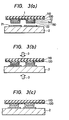
- the composite electrode member 1 and the GTO thyristor are connected in the following manner with reference to Figure 3.
- the composite electrode 1 and the GTO thyristor are disposed in parallel with each other so that the Sn layer 150 of the former and the cathode and gate electrodes 21, 22 of the latter face each other.
- the cathode and gate electrode foils 11 and 12 of the composite electrode member 1 are then registered with the patterns of the cathode and gate electrodes 11 and 12 of the GTO thyristor while observing through an optical microscope. Thereafter, the GTO thyristor and the composite electrode member 1 are heated to 190°C to 300°C as shown in Figure 3(b) and are bonded to each other.
- a pressure of 0.1 to 100 g/cm 2 is applied to the GTO thyristor and to the composite electrode 1 in the direction indicated by an arrow 3. It is preferred that an inert gas such as N 2 or Ar be blown to the bonding portion between the GTO thyristor and the composite electrode member 1 during bonding.
- the unitary structure of the GTO thyristor and the composite electrode member 1 is further heated as shown in Figure 3(.c) in order to mutually diffuse the Pb layer and constituent elements of a layer having the eutectic composition.
- this heating is effected at a temperature ranging from 330 to 360°C in the atmosphere of a reducing gas.
- the copper foil and the polyimide film are peeled off after this heat-treatment.
- Figure 4 illustrates the results of differential thermal analysis of the brazing material at the bond in the series of steps shown in Figure 3.
- Symbol (a) represents a differential thermal analysis (DTA) curve while (b) does a temperature.
- DTA differential thermal analysis
- FIG 4 shows that along with heating, exothermy by the etuectic reaction between Pb and Sn is observed at about 185 0 C and if heating is further effected, the slow exothermic reaction develops at a temperature ranging from 290°C to 320°C. It can be also seen that the exothermic reaction occurs at a tempera-0 ture in the range of from 300 to 320 C at the time o of cooling.
- the exothermy at 290 to 320 C results from fusing of the Pb and Sn layers and the exothermy at 300 to 320 C results from solidification of Pb-Sn solder.
- the heating temperature of bonding at the first stage in this embodiment is preferably o 0 from 190 C to 250 C.
- the most suitable temperature is in the proximity of the eutectic reaction. If the temperature of bonding at the first stage ex- o ceeds 250 C, the resulting eutectic crystal further reacts with the Pb layer, forming a diffusion layer. If the crystal grains are large as in the case in which the Pb layer is formed by the plating method, the diffusion layer is prefentially formed to the intercrystalline boundary of the crystal grains so that the crystal grains become easily separable and hence, bonding strength is reduced.
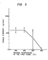
- Figure 5 illustrates tensile strength at the bond after bonding of Figure 3(b) is applied between the composite electrode member 1 and the GTO thyristor at various temperatures.
- the highest bonding strength can be obtained when the bonding temperature is within the range from a point close to the eutectic temperature (183 C) of Pb and Sn to about 250 C. 0 When the temperature exceeds 250 C, high bonding strength can no longer be obtained. Moreover, variance in bonding strength becomes greater, thus reducing the yield.
- the object of pressurization is to bring the Pb-Sn eutectic crystal, that occurs at the boundary between the Pb layer 140 and the Sn layer 150 at the first bonding step, into contact with the electrodes 21 and 22 of the GTO thyristor.
- the force of pressurization varies depending upon the surface smoothness of the Pb layer 140, the thickness of the Sn layer and the like but it is from tens to hundreds of g/cm 2 . This is the pressure that withstands the viscosity of the solder solution of the eutectic composition formed on the interface between the Pb and Sn layers. Accordingly, the force of pressurization is selected in accordance with the solder composition employed.
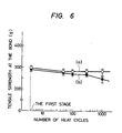
- the unitary structure of the GTO thyristor and the electrode plate connected to each other by the abovementioned method is subjected to a heat cycle 0 test using -55 C (for 25 minutes) - room temperature 0 (5 minutes) - 150 C (25 minutes) - room temperature (5 minutes) as one cycle.
- the results are shown in Figure 6.
- (a) represents the results of this embodiment and (b), those of a comparative example.
- a bonded structure of the composite electrode member 1 and the GTO thyristor in accordance with the conventional method using a homogeneous composition of 95 wt% Pb and 5 wt% Sn is used.
- the Pb layer 140 is interposed between the copper electrodes 11, 12 and the Sn layer 150 before bonding, and Sn diffuses into the Pb layer and reaches the adjacent portions of the electrodes 11 and 12 during bonding, especially by the second heat-treatment.
- the amount of Sn reaching the adjacent portions of the electrodes 11 and 12 is smaller in comparison with the case in which the conventional solder having the uniform distribution of Pb and Sn in advance is employed. For this reason, this embodiment provides higher resistance to heat fatigue.
- methods of heating the bonding portion between the composite electrode member 1 and the GTO thyristor include a method which disposes a heating mechanism on a bed for supporting the GTO thyristor, a method which heats the composite electrode member 1 from above its upper surface using an infrared ray converging lamp or heat blocks, and so forth.
- polyester tapes, glass epoxy tapes and the like may be used in place of the polyimide tape 110.
- An imide type adhesive may be used in place of the epoxy type adhesive 120.
- An Fe-Ni type alloy foil may be used in place of the copper foil.
- a metallic layer of In, Bi, Ag or the like as the simple substance or a metallic layer containing at least one of these elements may be used in place of the Pb layer 140.
- In, Bi or the like and the simple substance, alloys of Sn with these elements or alloys of Pb with these elements may be used in place of the Sn layer 150.
- An alloy having a substantially eutectic composition prepared in advance may be used at this portion.
- solder layers can be formed by various methods such as electrolytic wet plating, chemical wet plating, evaporation, dry plating, ion plating, spattering, and the like.
- the solder layer may be 1 to 100 Am thick. If the solder layer is a two-layered stnucture and consists of a Pb type solder as in the abovementioned embodiment, the thickness of the Pb layer 140 and Sn (or In, Bi) layer 150 is selected such that the atomic ratio Pb/Sn after bonding becomes 99.5/0.5 to 70/30.
- the present invention is not particularly limited thereto but can be of course applied to all the fields of semiconductor devices.
- the present invention is effective in obtaining a semiconductor device having external electrode connecting portions having high resistance to heat fatigue.
- the present invention is also effective in fabricating the semi- conductor device with an improved working property and with a higher level of reliability.
Abstract
Description
- This invention relates to a semiconductor device having external electrodes that are brazed to electrodes formed on a semiconductor substrate, and also to a method of fabricating such a semiconductor device.
- Generally, semiconductor devices have electrodes formed at predetermined portions on the surface of a semiconductor substrate and external electrodes for connecting the electrodes to the outside. The shapes of the external electrodes are diversified such as line-like, sheet-like, foil-like, and so forth. When these external electrodes are connected to the electrodes on the semiconductor surface with two-dimensional expansion, they are mostly connected to one another by brazing.
- If, in this case, the exothermic quantity on the semiconductor substrate is relatively great for handling relatively large power or for other reasons, a brazing material having a relatively high melting point and high resistance to heat fatigue is used as the brazing material..For instance, it has a composition of 95 wt% Pb and 5 wt/ Sn.
- However, a problem occurs from time to time that the_use of a brazing material having a high melting point fails to satisfy other characteristics of a semiconductor device or characteristics required in fabricating the semiconductor device. This point will be described more definitely.
- The inventors of the present invention previously proposed a semiconductor device which uses a metallic foil bonded to a resin tape as the external electrodes. In the semiconductor devices of this-kind, the electrodes of the semiconductor substrate and a metallic foil having substantially the same shape as that of the electrodes of the semiconductor substrate are disposed so as to oppose one another via a brazing material and the brazing material is then fused so as to bond them together. According to this arrangement, the metallic foil supplements the thickness of the electrodes of the semiconductor substrate, reduces the resistance of the electrodes as a whole and increases the current feed quantity even if the electrodes of the semiconductor substrate are thin and micro-small and hence, even if they alone can not provide a sufficient feed current quantity.
- If a solder having a high melting point is used for brazing such micro-small electrodes, however, the following problems are yet to be solved in conjunction with the working property. First, since the solder having a high melting point has a high treating temperature, the atmosphere for the treatment must be adjusted to a reducing atmosphere. In a non-reducing atmosphere, the solder and the electrode material of the semi-conductor substrate would be oxidized because the treating temperature is high and connection having high strength could not be obtained. It has been difficult from the aspect of fabrication of the device or from the aspect of the working property to adjust the atmosphere to a specific atmosphere and to connect the electrodes having a micro-small shape at a high temperature with a high level of accuracy.
- It has been clarified that even if the abovementioned problem were solved, another problem develops in that resistance to heat fatigue is not sufficiently high if connection is made in accordance with the conventional method using the solder having a high melting point. This is clarified by the inventors of the present invention in the course of evaluation of resistance to heat fatigue. It has been confirmed that the strength of even a solder having a high melting point drops down to an unpractical level after a large number of heat cycles are applied to the test-piece.
- It is an object of the present invention to provide a semiconductor device having external electrode connecting portions having high resistance to heat fatigue.
- The object of the fabrication method of a semi- conductor device in accordance with the present invention is to provide a fabrication method of a semi- conductor device which method employs a brazing method providing high resistance to heat fatigue, especially a brazing method having high working property as well as high reliability.
- One characterizing feature of the present invention resides in that the quantities of those elements, which are contained in a brazing material for connecting the electrodes on the semiconductor substrate to the external electrodes and react with the material of the electrodes or external electrodes thereby to form a hard and brittle compound, are smaller at the portion where the brazing material comes into contact with the electrodes or external electrodes than at the other portions.
- From the aspect of the fabrication method, the present invention is characterized in that an at least two-layered metallic layer is laminated and deposited on the surface of the electrodes on the semiconductor surface or that of the external electrodes, and both electrodes are opposed one another and are brought into intimate contact with one another via the metallic layer and are then bonded while they are being heated to a temperature near the eutectic temperature of an alloy consisting of the metals of the uppermost layer of the metallic layer and the metals of the layer below the uppermost layer and while force of pressure is being applied to both electrodes. The method of the present invention also includes a step of firmly bonding both electrodes by applying heat-treatment at a higher temperature than the abovementioned bonding temperature, whenever necessary.
- The present invention will be described in further detail. In the following description, the electrodes on the semiconductor substrate and the external electrodes will be referred to an "electrode film" and a "metallic foil" as a representative of the external electrodes, respectively, for ease of the explanation.
- In the semiconductor apparatus in accordance with the present invention, the metallic foil may be a metal or alloy having high conductivity or a metallic foil obtained by laminating the metal and the alloy. The metallic foil preferably contains at least one of Cu and Ni. The electrode film preferably contains a metal or metals other than Cu and Ni in at least its surface portion. However, the electrode film need not be a single layer but may assume a multi-layered structure in order to improve adhesion between the semiconductor substrate and these metals. In this case, metals including Cu or Ni may be used as the metal in the lower layer not appearing on the surface. For instance, the surface portion is made of Ag with the lower layer consisting of a laminate structure of Ni-Cr, Ni-Ti, Cu-Ni-Cr, Cu-Ni-Ti, or the like. It may consist of an alloy layer such as NiCr, NiTi, Cu-NiCr, Cu-NiTi or the like.
- The abovementioned metallic foil is bonded to the electrode film by use of a solder containing Pb and at least one of Sn, In and Bi. In the present invention, the distribution of Sn, In or Bi in this solder layer is heterogeneous so that the content of Sn, In or Bi is small in the metallic foil while the content of Sn, In or Bi is great in the electrode film.
- It has been clarified from the experiments carried out by the inventors of the present invention that when the Cu- or Ni-containing metallic foil is bonded to the electrode film by soldering, bond is likely to peel off due to heat fatigue and bonding strength is likely to drop to cause inferior bonding when this semiconductor device is subjected to a power cycle test and a heat cycle test. The reasons for the peel and drop of bond- ing strength are assumed as follows. When the heat cycle or power cycle is applied, a new metallic phase is generated in the region adjacent the metallic foil, the resulting metallic phase is hard and brittle and the formation of this metallic phase changes the composition and structure of the solder layer. It has also been clarified that the Cu- or Ni-containing metallic foil forms the metallic phase together with Sn, In or Bi but does not with Pb.
- When the Cu foil is used as the metallic foil and a Pn-Sn type, a Pb-In type or a Pb-Bi type is used as the solder, Cu6 Sn5 and Cu3Sn are formed in the Pb-Sn system, CuBi is formed in the Pb-In system and Cu9In4, Cu4In and CU7In4 are formed in the Pb-Bi system. When a Ni-containing foil is used as the metallic foil, Ni3Sn4, Ni3Sn2, Ni4 Sn and NiSn are formed in the Pb-Sn system, NiBi is formed in the Pb-Bi system and In27Ni10, In3Ni2, InNi, InNi3 and InNi4 are formed in the Pb-In system.
- These metallic phases are formed as Sn, In and Bi diffuse from the solder layer and reach the boundary with the metallic foil along with the application of the heat cycle. It has been found that diffusion is accelerated by the stress of the bond portion arising not only from the temperature condition but also from the mutual difference of expansion coefficients of the bonded matter. This is because the diffusion of these metals is fast in the field of stress.
- Next, the method of the present invention will be described in detail.
- In accordance with the method of the present invention, the constituent elements of each metal are disposed in a laminar form in a predetermined sequence on the electrode film or the metallic foil so as to attain a desired solder composition.when the final heat-treatment is effected. In this case, the elements are arranged such that an eutectic composition is partially formed between the uppermost layer and the next layer with respect to the direction of lamination. Next, the electrode film and the metallic foil are opposed to each other and the eutectic reaction is carried out between the uppermost layer and the next layer to form a fusing solution at that portion. Under this state, both electrode film and metallic foil are pressurized and are heat-bonded under pressure by means of the fusing solution of the abovementioned eutectic composition. In this manner, the electrode film and the metallic foil can be continuously bonded at a relatively low temperature with a high working property. Since the treating temperature at the time of bonding is low, oxidation of the members and solder hardly occurs and the atmosphere for the treatment may be sufficiently established by spraying a gas having low reducing power such as N2 or Ar to the bonding portion.
- The abovementioned bonding step alone can provide sufficiently high bonding strength, but in order to obtain the brazing layer having a solder composition of a high melting point, the brazing material layer is as a whole heated and turned into a fusing solution at a temperature higher than the melting point each of the uppermost layer and subsequent metallic layers so that the metals of the uppermost and subsequent layers are mutually diffused to form an alloy layer. In this case, since the electrode film and the metallic foil are already bonded mechanically sufficiently, mutual deviation can be checked without applying any load or by applying a low load to the bonded portion.
- The distribution of each element in the abovementioned alloy is determined by the diffusion phenomenon of each element at the time of second heating. If those elements which form the hard and brittle alloy phase with Cu or Ni are arranged in advance so that they do not come into direct contact with the Cu or Ni member, the formation of the alloy phase in the proximity of the Cu or Ni member is limited to the quantities of the elements that are diffused to this portion.
-
- Figure 1 illustrates a composite electrode member to be used in one embodiment of the present invention;
- Figure 2 illustrates a gate turn-off,(GTO) thyristor to which one embodiment of the present invention is applied;
- Figure 3 diagrammatically illustrates the production steps in accordance with one embodiment of the present invention;
- Figure 4 is a DTA diagram in the fabrication method of one embodiment of the present invention; and
- Figures 5 and 6 are diagrams that are useful for explaining the effects of one embodiment of the present invention.
- Hereinafter, preferred embodiments of the present invention will be described.
- Figure l(a) is a plan view of the composite electrode member to be used in one embodiment of the present invention and Figure l(b) is an enlarged sectional view of the electrode member taken along line A - A' of Figure l(a). In Figure 1, the
composite electrode member 1 is obtained by bonding a 35 µm thick copper foil having a width W2 of 25 mm to a 75 µmthick polyimide tape 110 having a width W of 35 mm by use of anepoxy type adhesive 120 and then etching the copper foil in a predetermined pattern. The pattern of the copper foil is such that a pair ofexternal electrodes bridge portion 13 to electrically short- circuit the pair of external electrodes at the portions other than the portions of the external electrodes are repeated in the longitudinal direction of the copper foil. Accordingly, the region represented byreference numeral 14 in Figure l(a) does not exist.Reference numeral 15 represents punch holes (perforation) for feeding the tape.Portions 16 at which theelectrodes - As shown in Figure l(b), a
Pb layer 140 and anSn layer 150 are formed on this copper foil pattern in predetermined thickness by electro-plating. ThePb layer 140 is 18 µm to 20µm thick while theSn layer 150 is 1 µm to 3 µm thick. In performing the electro-plating, theabovementioned bridge portion 13 plays the part of reducing the number of electrode connecting portions to the copper foil. - The
composite electrode member 1 in which the copper foil is shaped in a predetermined pattern in accordance with the abovementioned method is used as the cathode external electrode and gate external electrode of a gate turn-off (GTO) thyristor in this embodiment. Figure 2 shows the structure of the GTO thyristor used in this embodiment. Figure 2(a) is a plan view and 2(b) is a sectional view taken along line B - B' of 2(a). In this GTO thyristor, both cathode andgate electrodes main surface 201 of thesemiconductor substrate 2. Thesemiconductor substrate 2 has a four-layered laminate structure extending from the othermain surface 202 to onemain surface 201 and consisting of a p-type emitter layer PE (or anode layer), an n-type base layer nE, p-type base layer PB (or gate layer) and an n-type emitter layer nE (or cathode layer). Agroove 24 is defined around the peripheral portion of onemain surface 201 and glass for passivation is packed into thegroove 24. Ananode electrode 23 is formed over the entire surface of the othermain surface 202. - The
cathode electrode 21, thegate electrode 22 and theanode electrode 23 can be soldered and use a metallic film that satisfies the requirements such as high ohmic contact with p- and n-type silicon, good adhesion with the semiconductor substrate, low resistivity, and so forth. In this embodiment, a Cr-Ni-Ag multi-layered metallic film is used and thecathode electrode 21 as well as thegate electrode 22 are formed by lift-off process. - The
composite electrode member 1 and the GTO thyristor are connected in the following manner with reference to Figure 3. As shown in Figure 3(a), thecomposite electrode 1 and the GTO thyristor are disposed in parallel with each other so that theSn layer 150 of the former and the cathode andgate electrodes composite electrode member 1 are then registered with the patterns of the cathode andgate electrodes composite electrode member 1 are heated to 190°C to 300°C as shown in Figure 3(b) and are bonded to each other. In this instance, a pressure of 0.1 to 100 g/cm2 is applied to the GTO thyristor and to thecomposite electrode 1 in the direction indicated by anarrow 3. It is preferred that an inert gas such as N2 or Ar be blown to the bonding portion between the GTO thyristor and thecomposite electrode member 1 during bonding. - Next, the unitary structure of the GTO thyristor and the
composite electrode member 1 is further heated as shown in Figure 3(.c) in order to mutually diffuse the Pb layer and constituent elements of a layer having the eutectic composition. Under the state in which a load is being applied, this heating is effected at a temperature ranging from 330 to 360°C in the atmosphere of a reducing gas. The copper foil and the polyimide film are peeled off after this heat-treatment. - Figure 4 illustrates the results of differential thermal analysis of the brazing material at the bond in the series of steps shown in Figure 3. Symbol (a) represents a differential thermal analysis (DTA) curve while (b) does a temperature. It can be seen from Figure 4 that along with heating, exothermy by the etuectic reaction between Pb and Sn is observed at about 1850C and if heating is further effected, the slow exothermic reaction develops at a temperature ranging from 290°C to 320°C. It can be also seen that the exothermic reaction occurs at a tempera-0 ture in the range of from 300 to 320 C at the time o of cooling. The exothermy at 290 to 320 C results from fusing of the Pb and Sn layers and the exothermy at 300 to 320 C results from solidification of Pb-Sn solder.
- The heating temperature of bonding at the first stage in this embodiment (Figure 3(b)) is preferably o 0 from 190 C to 250 C. The most suitable temperature is in the proximity of the eutectic reaction. If the temperature of bonding at the first stage ex- o ceeds 250 C, the resulting eutectic crystal further reacts with the Pb layer, forming a diffusion layer. If the crystal grains are large as in the case in which the Pb layer is formed by the plating method, the diffusion layer is prefentially formed to the intercrystalline boundary of the crystal grains so that the crystal grains become easily separable and hence, bonding strength is reduced.
- Figure 5 illustrates tensile strength at the bond after bonding of Figure 3(b) is applied between the
composite electrode member 1 and the GTO thyristor at various temperatures. The highest bonding strength can be obtained when the bonding temperature is within the range from a point close to the eutectic temperature (183 C) of Pb and Sn to about 250 C. 0 When the temperature exceeds 250 C, high bonding strength can no longer be obtained. Moreover, variance in bonding strength becomes greater, thus reducing the yield. - In the first bonding step, heating to a predetermined temperature and pressurization of the bonding portion are effected as described already. The object of pressurization is to bring the Pb-Sn eutectic crystal, that occurs at the boundary between the
Pb layer 140 and theSn layer 150 at the first bonding step, into contact with theelectrodes Pb layer 140, the thickness of the Sn layer and the like but it is from tens to hundreds of g/cm2. This is the pressure that withstands the viscosity of the solder solution of the eutectic composition formed on the interface between the Pb and Sn layers. Accordingly, the force of pressurization is selected in accordance with the solder composition employed. - The unitary structure of the GTO thyristor and the electrode plate connected to each other by the abovementioned method is subjected to a heat cycle 0 test using -55 C (for 25 minutes) - room temperature 0 (5 minutes) - 150 C (25 minutes) - room temperature (5 minutes) as one cycle. The results are shown in Figure 6. In this drawing, (a) represents the results of this embodiment and (b), those of a comparative example. As the comparative example, a bonded structure of the
composite electrode member 1 and the GTO thyristor in accordance with the conventional method using a homogeneous composition of 95 wt% Pb and 5 wt% Sn is used. - It can be seen from Figure 6 that tensile strength drops gradually with an increasing number of heat cycles in the comparative example (b) but the rate of drop is smaller in (a) than in (b): This tendency becomes more remarkable when the number of heat cycles increases. It can be thus appareciated that the semiconductor device in accordance with the present invention has higher resistance to heat fatigue. The reason why such a result can be obtained is that a hard and brittle metallic phase can not easily be formed at the boundary between the solder and the metal to be bonded in accordance with the present invention, as described already. More definitely, in this embodiment, the
Pb layer 140 is interposed between thecopper electrodes Sn layer 150 before bonding, and Sn diffuses into the Pb layer and reaches the adjacent portions of theelectrodes electrodes - In the abovementioned embodiment, methods of heating the bonding portion between the
composite electrode member 1 and the GTO thyristor include a method which disposes a heating mechanism on a bed for supporting the GTO thyristor, a method which heats thecomposite electrode member 1 from above its upper surface using an infrared ray converging lamp or heat blocks, and so forth. - The abovementioned embodiment can be modified in various manners. First, polyester tapes, glass epoxy tapes and the like may be used in place of the
polyimide tape 110. An imide type adhesive may be used in place of theepoxy type adhesive 120. An Fe-Ni type alloy foil may be used in place of the copper foil. - A metallic layer of In, Bi, Ag or the like as the simple substance or a metallic layer containing at least one of these elements may be used in place of the
Pb layer 140. Furthermore, In, Bi or the like and the simple substance, alloys of Sn with these elements or alloys of Pb with these elements may be used in place of theSn layer 150. An alloy having a substantially eutectic composition prepared in advance may be used at this portion. - These metallic layers can be formed by various methods such as electrolytic wet plating, chemical wet plating, evaporation, dry plating, ion plating, spattering, and the like. The solder layer may be 1 to 100 Am thick. If the solder layer is a two-layered stnucture and consists of a Pb type solder as in the abovementioned embodiment, the thickness of the
Pb layer 140 and Sn (or In, Bi)layer 150 is selected such that the atomic ratio Pb/Sn after bonding becomes 99.5/0.5 to 70/30. - If Ag, Ni or the like is deposited on the copper foil bonded to the composite electrode member and the solder material layer is then formed thereon, wettability with respect to the solder material can be preferably improved.
- Although the foregoing description deals with the example in which the present invention is applied to the GTO thyristor having the micro-small electrode structure, the present invention is not particularly limited thereto but can be of course applied to all the fields of semiconductor devices.
- As described in the foregoing, the present invention is effective in obtaining a semiconductor device having external electrode connecting portions having high resistance to heat fatigue. The present invention is also effective in fabricating the semi- conductor device with an improved working property and with a higher level of reliability.
Claims (6)
Applications Claiming Priority (2)
| Application Number | Priority Date | Filing Date | Title |
|---|---|---|---|
| JP137011/81 | 1981-09-02 | ||
| JP56137011A JPS5839047A (en) | 1981-09-02 | 1981-09-02 | Semiconductor device and manufacture thereof |
Publications (3)
| Publication Number | Publication Date |
|---|---|
| EP0073383A2 true EP0073383A2 (en) | 1983-03-09 |
| EP0073383A3 EP0073383A3 (en) | 1984-08-08 |
| EP0073383B1 EP0073383B1 (en) | 1987-06-10 |
Family
ID=15188722
Family Applications (1)
| Application Number | Title | Priority Date | Filing Date |
|---|---|---|---|
| EP19820107381 Expired EP0073383B1 (en) | 1981-09-02 | 1982-08-13 | Semiconductor device having external electrodes bonded to electrodes on a semiconductor substrate and method of fabricating such a semiconductor device |
Country Status (4)
| Country | Link |
|---|---|
| US (1) | US4651191A (en) |
| EP (1) | EP0073383B1 (en) |
| JP (1) | JPS5839047A (en) |
| DE (1) | DE3276556D1 (en) |
Cited By (3)
| Publication number | Priority date | Publication date | Assignee | Title |
|---|---|---|---|---|
| EP0266093A2 (en) * | 1986-10-27 | 1988-05-04 | Electric Power Research Institute, Inc | Process of making a high power multi-layer semiconductive switching device with multiple parallel contacts |
| EP0568995A2 (en) * | 1992-05-06 | 1993-11-10 | Sumitomo Electric Industries, Limited | Semiconductor device with bumps |
| WO1996016442A1 (en) * | 1994-11-17 | 1996-05-30 | Fraunhofer-Gesellschaft zur Förderung der angewandten Forschung e.V. | Core metal soldering knob for flip-chip technology |
Families Citing this family (21)
| Publication number | Priority date | Publication date | Assignee | Title |
|---|---|---|---|---|
| DE3523808C3 (en) | 1984-07-03 | 1995-05-04 | Hitachi Ltd | Process for soldering parts of an electronic arrangement made of different materials and its use |
| US4786962A (en) * | 1986-06-06 | 1988-11-22 | Hewlett-Packard Company | Process for fabricating multilevel metal integrated circuits and structures produced thereby |
| US5023700A (en) * | 1988-06-17 | 1991-06-11 | Ngk Insulators, Ltd. | Minutely patterned structure |
| US4935627A (en) * | 1989-03-13 | 1990-06-19 | Honeywell Inc. | Electrical interconnection apparatus for achieving precise alignment of hybrid components |
| US5175609A (en) * | 1991-04-10 | 1992-12-29 | International Business Machines Corporation | Structure and method for corrosion and stress-resistant interconnecting metallurgy |
| US5266522A (en) * | 1991-04-10 | 1993-11-30 | International Business Machines Corporation | Structure and method for corrosion and stress-resistant interconnecting metallurgy |
| JPH0547812A (en) * | 1991-08-19 | 1993-02-26 | Mitsubishi Electric Corp | Semiconductor device |
| JP3054021B2 (en) * | 1993-12-27 | 2000-06-19 | 株式会社東芝 | Compound semiconductor device |
| US6828668B2 (en) * | 1994-07-07 | 2004-12-07 | Tessera, Inc. | Flexible lead structures and methods of making same |
| US6117694A (en) * | 1994-07-07 | 2000-09-12 | Tessera, Inc. | Flexible lead structures and methods of making same |
| US6361959B1 (en) | 1994-07-07 | 2002-03-26 | Tessera, Inc. | Microelectronic unit forming methods and materials |
| FI98899C (en) * | 1994-10-28 | 1997-09-10 | Jorma Kalevi Kivilahti | Method for connecting electronic components by soldering |
| US5763941A (en) * | 1995-10-24 | 1998-06-09 | Tessera, Inc. | Connection component with releasable leads |
| US6261863B1 (en) | 1995-10-24 | 2001-07-17 | Tessera, Inc. | Components with releasable leads and methods of making releasable leads |
| US6025649A (en) | 1997-07-22 | 2000-02-15 | International Business Machines Corporation | Pb-In-Sn tall C-4 for fatigue enhancement |
| WO2000057472A1 (en) * | 1999-03-24 | 2000-09-28 | Infineon Technologies Ag | Method of connecting a connecting wire to a contact of an integrated circuit |
| JP4293500B2 (en) * | 2001-05-07 | 2009-07-08 | 第一電子工業株式会社 | Manufacturing method of electronic parts |
| JP2003303842A (en) * | 2002-04-12 | 2003-10-24 | Nec Electronics Corp | Semiconductor device and manufacturing method therefor |
| KR100568496B1 (en) * | 2004-10-21 | 2006-04-07 | 삼성전자주식회사 | Film circuit substrate having sn-in alloy layer |
| KR101184108B1 (en) * | 2008-05-02 | 2012-09-18 | 후지쯔 가부시끼가이샤 | Wiring board, process for producing the same, and process for manufacturing electronic device |
| US11088308B2 (en) * | 2019-02-25 | 2021-08-10 | Tdk Corporation | Junction structure |
Citations (3)
| Publication number | Priority date | Publication date | Assignee | Title |
|---|---|---|---|---|
| JPS53137055A (en) * | 1977-05-04 | 1978-11-30 | Hitachi Ltd | Solder |
| EP0009131A1 (en) * | 1978-09-20 | 1980-04-02 | International Business Machines Corporation | Process for in situ modification of solder alloy compositions |
| JPS5646583A (en) * | 1979-09-21 | 1981-04-27 | Denki Onkyo Co Ltd | Semiconductor device and manufacture thereof |
Family Cites Families (3)
| Publication number | Priority date | Publication date | Assignee | Title |
|---|---|---|---|---|
| US3401055A (en) * | 1964-12-31 | 1968-09-10 | Ibm | Vapor depositing solder |
| US3436818A (en) * | 1965-12-13 | 1969-04-08 | Ibm | Method of fabricating a bonded joint |
| US3839727A (en) * | 1973-06-25 | 1974-10-01 | Ibm | Semiconductor chip to substrate solder bond using a locally dispersed, ternary intermetallic compound |
-
1981
- 1981-09-02 JP JP56137011A patent/JPS5839047A/en active Granted
-
1982
- 1982-08-13 EP EP19820107381 patent/EP0073383B1/en not_active Expired
- 1982-08-13 DE DE8282107381T patent/DE3276556D1/en not_active Expired
-
1986
- 1986-06-25 US US06/880,942 patent/US4651191A/en not_active Expired - Fee Related
Patent Citations (3)
| Publication number | Priority date | Publication date | Assignee | Title |
|---|---|---|---|---|
| JPS53137055A (en) * | 1977-05-04 | 1978-11-30 | Hitachi Ltd | Solder |
| EP0009131A1 (en) * | 1978-09-20 | 1980-04-02 | International Business Machines Corporation | Process for in situ modification of solder alloy compositions |
| JPS5646583A (en) * | 1979-09-21 | 1981-04-27 | Denki Onkyo Co Ltd | Semiconductor device and manufacture thereof |
Non-Patent Citations (4)
| Title |
|---|
| IBM TECHNICAL DISCLOSURE BULLETIN, vol. 19, no. 1, June 1976, page 174, New York, US; G. DiGIACOMO et al.: "Circuit module interconnection". * |
| IEEE TRANSACTIONS ON PARTS, HYBRIDS, AND PACKAGING, vol. PHP-13, no. 3, September 1977, pages 194-198, New York, US; L.S. GOLDMANN et al.: "Lead-indium for controlled-collapse chip joining". * |
| PATENTS ABSTRACTS OF JAPAN, vol. 3, no. 14, 8th February 1979, page 2 C 36 & JP-A-53 137 055 (HITACHI SEISAKUSHO K.K.) 30-11-1978 * |
| PATENTS ABSTRACTS OF JAPAN, vol. 5, no. 103 (E-64)[775], 3rd July 1981 & JP-A-56 046 583 (DENKI ONKIYOU K.K.) 27-04-1981 * |
Cited By (6)
| Publication number | Priority date | Publication date | Assignee | Title |
|---|---|---|---|---|
| EP0266093A2 (en) * | 1986-10-27 | 1988-05-04 | Electric Power Research Institute, Inc | Process of making a high power multi-layer semiconductive switching device with multiple parallel contacts |
| EP0266093A3 (en) * | 1986-10-27 | 1988-09-28 | Electric Power Research Institute, Inc | High power multi-layer semiconductive switching device with multiple parallel contacts |
| EP0568995A2 (en) * | 1992-05-06 | 1993-11-10 | Sumitomo Electric Industries, Limited | Semiconductor device with bumps |
| EP0568995A3 (en) * | 1992-05-06 | 1993-12-08 | Sumitomo Electric Industries, Limited | Semiconductor device with bumps |
| US5461261A (en) * | 1992-05-06 | 1995-10-24 | Sumitomo Electric Industries, Ltd. | Semiconductor device with bumps |
| WO1996016442A1 (en) * | 1994-11-17 | 1996-05-30 | Fraunhofer-Gesellschaft zur Förderung der angewandten Forschung e.V. | Core metal soldering knob for flip-chip technology |
Also Published As
| Publication number | Publication date |
|---|---|
| DE3276556D1 (en) | 1987-07-16 |
| EP0073383B1 (en) | 1987-06-10 |
| US4651191A (en) | 1987-03-17 |
| EP0073383A3 (en) | 1984-08-08 |
| JPH0136254B2 (en) | 1989-07-31 |
| JPS5839047A (en) | 1983-03-07 |
Similar Documents
| Publication | Publication Date | Title |
|---|---|---|
| EP0073383B1 (en) | Semiconductor device having external electrodes bonded to electrodes on a semiconductor substrate and method of fabricating such a semiconductor device | |
| JP3320979B2 (en) | How to mount a device directly on a device carrier | |
| JP3262497B2 (en) | Chip mounted circuit card structure | |
| US4463059A (en) | Layered metal film structures for LSI chip carriers adapted for solder bonding and wire bonding | |
| KR940001149B1 (en) | Chip bonding method of semiconductor device | |
| US4482912A (en) | Stacked structure having matrix-fibered composite layers and a metal layer | |
| EP0513521A2 (en) | Planarized thin film surface covered wire bonded semiconductor package | |
| IE52529B1 (en) | Method of simultaneously manufacturing multiple electrical connections between two elements | |
| JPS6231819B2 (en) | ||
| US7670879B2 (en) | Manufacturing method of semiconductor module including solid-liquid diffusion joining steps | |
| JP2533227B2 (en) | Thermocompression bonding member and manufacturing method thereof | |
| US5206186A (en) | Method for forming semiconductor electrical contacts using metal foil and thermocompression bonding | |
| EP0416847A2 (en) | Methods of joining components | |
| US5184206A (en) | Direct thermocompression bonding for thin electronic power chips | |
| EP0135416B1 (en) | Integrated circuit having a pre-attached conductive mounting media and method of making the same | |
| EP0186818A2 (en) | Chip to pin interconnect method | |
| JP3297177B2 (en) | Method for manufacturing semiconductor device | |
| US6024274A (en) | Method for tape automated bonding to composite bumps | |
| EP0167030B1 (en) | Method of forming solder interconnections for semiconductor devices | |
| CA1244147A (en) | Die bonding process | |
| JP3284034B2 (en) | Semiconductor device and manufacturing method thereof | |
| JP2709499B2 (en) | Semiconductor element connection structure | |
| JPH061789B2 (en) | Film carrier for semiconductor device | |
| JPS63185035A (en) | Semiconductor device | |
| US6884708B2 (en) | Method of partially plating substrate for electronic devices |
Legal Events
| Date | Code | Title | Description |
|---|---|---|---|
| PUAI | Public reference made under article 153(3) epc to a published international application that has entered the european phase |
Free format text: ORIGINAL CODE: 0009012 |
|
| AK | Designated contracting states |
Designated state(s): CH DE FR GB IT LI NL SE |
|
| PUAL | Search report despatched |
Free format text: ORIGINAL CODE: 0009013 |
|
| AK | Designated contracting states |
Designated state(s): CH DE FR GB IT LI NL SE |
|
| 17P | Request for examination filed |
Effective date: 19840816 |
|
| GRAA | (expected) grant |
Free format text: ORIGINAL CODE: 0009210 |
|
| AK | Designated contracting states |
Kind code of ref document: B1 Designated state(s): CH DE FR GB IT LI NL SE |
|
| REF | Corresponds to: |
Ref document number: 3276556 Country of ref document: DE Date of ref document: 19870716 |
|
| ET | Fr: translation filed | ||
| ITF | It: translation for a ep patent filed |
Owner name: MODIANO & ASSOCIATI S.R.L. |
|
| PLBE | No opposition filed within time limit |
Free format text: ORIGINAL CODE: 0009261 |
|
| STAA | Information on the status of an ep patent application or granted ep patent |
Free format text: STATUS: NO OPPOSITION FILED WITHIN TIME LIMIT |
|
| 26N | No opposition filed | ||
| ITTA | It: last paid annual fee | ||
| PGFP | Annual fee paid to national office [announced via postgrant information from national office to epo] |
Ref country code: FR Payment date: 19930818 Year of fee payment: 12 |
|
| PGFP | Annual fee paid to national office [announced via postgrant information from national office to epo] |
Ref country code: NL Payment date: 19930831 Year of fee payment: 12 |
|
| PGFP | Annual fee paid to national office [announced via postgrant information from national office to epo] |
Ref country code: CH Payment date: 19931028 Year of fee payment: 12 |
|
| PG25 | Lapsed in a contracting state [announced via postgrant information from national office to epo] |
Ref country code: LI Effective date: 19940831 Ref country code: CH Effective date: 19940831 |
|
| PGFP | Annual fee paid to national office [announced via postgrant information from national office to epo] |
Ref country code: SE Payment date: 19940831 Year of fee payment: 13 |
|
| EAL | Se: european patent in force in sweden |
Ref document number: 82107381.4 |
|
| PG25 | Lapsed in a contracting state [announced via postgrant information from national office to epo] |
Ref country code: NL Effective date: 19950301 |
|
| NLV4 | Nl: lapsed or anulled due to non-payment of the annual fee | ||
| PG25 | Lapsed in a contracting state [announced via postgrant information from national office to epo] |
Ref country code: FR Effective date: 19950428 |
|
| REG | Reference to a national code |
Ref country code: CH Ref legal event code: PL |
|
| REG | Reference to a national code |
Ref country code: FR Ref legal event code: ST |
|
| PG25 | Lapsed in a contracting state [announced via postgrant information from national office to epo] |
Ref country code: SE Effective date: 19950814 |
|
| EUG | Se: european patent has lapsed |
Ref document number: 82107381.4 |
|
| PGFP | Annual fee paid to national office [announced via postgrant information from national office to epo] |
Ref country code: GB Payment date: 19960802 Year of fee payment: 15 |
|
| PGFP | Annual fee paid to national office [announced via postgrant information from national office to epo] |
Ref country code: DE Payment date: 19961029 Year of fee payment: 15 |
|
| PG25 | Lapsed in a contracting state [announced via postgrant information from national office to epo] |
Ref country code: GB Free format text: LAPSE BECAUSE OF NON-PAYMENT OF DUE FEES Effective date: 19970813 |
|
| GBPC | Gb: european patent ceased through non-payment of renewal fee |
Effective date: 19970813 |
|
| PG25 | Lapsed in a contracting state [announced via postgrant information from national office to epo] |
Ref country code: DE Free format text: LAPSE BECAUSE OF NON-PAYMENT OF DUE FEES Effective date: 19980501 |