EP0082981A2 - Memory system with selective assignment of spare locations - Google Patents
Memory system with selective assignment of spare locations Download PDFInfo
- Publication number
- EP0082981A2 EP0082981A2 EP82111123A EP82111123A EP0082981A2 EP 0082981 A2 EP0082981 A2 EP 0082981A2 EP 82111123 A EP82111123 A EP 82111123A EP 82111123 A EP82111123 A EP 82111123A EP 0082981 A2 EP0082981 A2 EP 0082981A2
- Authority
- EP
- European Patent Office
- Prior art keywords
- memory
- bit
- data
- defective
- main memory
- Prior art date
- Legal status (The legal status is an assumption and is not a legal conclusion. Google has not performed a legal analysis and makes no representation as to the accuracy of the status listed.)
- Granted
Links
Images


Classifications
-
- G—PHYSICS
- G11—INFORMATION STORAGE
- G11C—STATIC STORES
- G11C29/00—Checking stores for correct operation ; Subsequent repair; Testing stores during standby or offline operation
- G11C29/70—Masking faults in memories by using spares or by reconfiguring
- G11C29/76—Masking faults in memories by using spares or by reconfiguring using address translation or modifications
Definitions
- This invention relates to digital data memory systems in which defective storage locations are logically replaced by storage locations in alternate memory units.
- the memory address means is arranged such that any addressable storage location which contains a defect is merely bypassed.
- an auxiliary memory is employed to store data that would normally be stored at a location in the main memory that contained a defect. Suitable circuitry is then provided to recognize when a defect location is being addressed so that the data being entered can be stored in the auxiliary memory or, if data is being read from memory, the data from the auxiliary memory is provided in place of data from the main memory.
- the prior art has also long recognized that data being stored in the memory can be protected against errors by a suitable error correcting system wherein check characters are generated as the data is being entered into the memory and are then stored with the data so that when the data is subsequently read out and check characters are again generated,.the system can detect the presence of errors, the type of error, and the location of the error by processing the various check characters so that the error can then be corrected before the data is further processed by the system.
- the number of check characters that are associated with the word of data that is stored in memory depends on the power of the ECC code employed. Generally, however, as the number of error types that have to be corrected increases, so do the number of check characters that have to be generated and stored with the data word.
- the object of the present invention to provide a memory system for storing data in which a minimum amount of auxiliary storage is required to store data that cannot be stored in defective locations of the main memory, in which defective locations in main memory are replaced on a logical basis without impacting system performance, in which defective locations in main memory are mapped to good spare locations in an alternate memory by means of a relatively small index, and which is characterized by means for selectively assigning replacement storage positions in.an auxiliary memory in accordance with the pattern of defective storage locations in the main memory and the error patterns that are correctable by an associated error correcting system.
- the present invention provides a memory system using a main memory with defective storage locations which permits each system to be optimized in accordance with the number and location of defective positions of the main memory by providing means for selectively controlling which defective locations of the main memory unit are logically replaced with good locations in an auxiliary memory so the reading of a data word into the system from that location with an uncorrectable error is avoided.
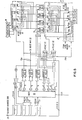
- the data processing system shown in FIG. 1 comprises a host data processing CPU 10, a main memory system 11, and a secondary memory 13 which is connected between CPU 10 and memory system 11.
- a data bus 14 extends from the CPU 10 into the system 11 through the secondary unit 13.
- an input data bus 15 extends from the main data storage system 11 to the CPU 10 through the unit 13.
- Address bus 20 also extends from the CPU 10 to the main data storage system 11 and to the unit 13.
- a control bus 21 provides control data to the unit 13 from the CPU 10.
- An error correcting system 22 is associated with the input bus 15 and output bus 14 and functions to generate error correcting check characters for each data word transferred from the CPU 10 to system 11 and transferred from the system 11 over the output bus 15 to the CPU 10.
- the ECC system 22 functions to correct predetermined types of errors which result either from defective storage locations being involved in the transfer or a random error occurring for any number of valid technical reasons.
- the embodiment of the invention to be described involves data words having 144 bit positions, as shown in FIG. 2, which comprise 128 data bit positions and 16 check bit positions.
- the main data storage system 11 comprises a main memory 30 which is shown in FIG. la and which consists of an array of 64 chips for each bit position of the 144-bit word shown in FIG. 2, with each chip containing 64K bit cell.s.
- the memory therefore, stores 64 K data words of 144 bits each.
- the storage address bus 20 is 22 bits wide to define one of 64 2 K word locations.
- the main memory is susceptible to various errors, some of which are represented in FIGS. 3a-3c.
- FIG. 3a one chip of 64K bit cells is defective. It is associated with bit position 27.
- FIG. 3b one row of chip 1, associated with bit position 25, is shown as defective, making 256 contiguous addresses defective.
- FIG. 3c shows a smaller defect area in chip 4 associated with bit position 28 at bit cell positions 3 and 4, and also at a defective column at bit cell locations 257-512.
- FIG. 4 The portion of FIG. 4 within the dotted box 29 is one of 36 identical alternate data storage sections also referred to as replacement units. Each section comprises two alternate memories 31 and 32.
- a write multiplexer 33 is disposed between four lines of the.output bus 14 from the CPU 10 and alternate memories,31 and 32.
- Output multiplexer 34 is connected between the outputs of the main memory 30 and alternate memories 31'and 32 and four lines of the input bus 15 to the CPU 10.
- the address bus 20 is connected to the main data storage unit 30 and to the selection control unit 36 which also receives the control bus 21 from the CPU .10.
- Output control lines 39A-39D from block 36 extend to both.alternate memories 31 and 32 and both multiplexers 33 and 34.
- the selection control block 36 functions generally to address locations in the alternate memory units 31 and 32 to replace defective bit cells in the main memory 30.
- the main memory 30 consists of 144 separate memory arrays of 64 chips which are arranged such that a data word consisting of 144 bit positions is stored in a manner that each bit is failure independent of all the other bits.
- the defective chip may be entirely replaced by another 64K chip in one of the alternate storage units 31 or 32.
- a 16-bit address supplied to each chip functions to select the same bit cell on each chip.
- the chip may be envisioned as comprising a matrix of 256 rows and 256 columns such that an 8-bit byte defines one of 256 rows and another 8-bit byte defines one of 256 columns and together the 16 bits define one bit cell at the intersection of a row and a column.
- An additional 6 bits are required to select one of the 64 chips associated with each bit position of the data word.
- the address bus 20 shown in FIGS. 1 and 4 therefore,'-consists of 22 bits.
- Input data bus 14 extending from the CPU 10 is 144-bits wide, as is the output bus 15 to the CPU 10.
- a 144-bit word is transferred into main memory 30 by input bus 14 and stored at the location defined by the 22 - bit address supplied on address bus 20.
- the transfer of data from main storage 30 is accomplished by again supplying the 22-bit address on address bus 20 which transfers the 144 data bits through the output multiplexers 34 of each replacement unit 29 to the output bus 15.
- the selection unit 36 of FIG. 4 comprises an index unit 50 which is provided with two input address busses 51 and 52 and the control input- bus 21 from the CPU 10.
- Input busses 51 and 52 are each 6-bit busses which are derived from a part of the 22-bit address from data bus 20 that is used to address a location in the main memory 30.
- the function of the index unit 50 is to generate an address for the alternate storage units 31 and 32 and to provide control type. signals to the section which define the operation or control mode of each replacement unit 29.
- the index 50 of each replacement unit therefore, comprises a writable memory that can store a portion of the address data and the control data.
- the size of the index unit will be dependent on various parameters, such as the size of the main memory, the reliability, the amount of defects in the main memory, and the size of the defects to be replaced.
- the index may, therefore, consist of two 4K x 8 memory modules.
- Each of the memory modules is supplied with a 12-bit address to provide a 16-bit output from the index 50. Therefore, the input busses 51 and 52 to the index 50 are 6 bits each, while the output provided from the index is 16 bits, 14 of which are used for the various fields which are shown in FIG. 6, including field E, which becomes part of the address for the alternate memories 31 and 32.
- the alternate data storage unit 31 shown in FIG. 5 has four chips. Units 31 and 32 provide the replacement spares for bit positions 25-28 of the data word and can be used to replace various fault areas in main memory chips associated with bit positions 25-28.
- the location of the defective memory cells are supplied to the index 50 from the CPU 10 over the control signal bus 21 and, as will be explained later, does not necessarily include all defective cell locations of any size in the main memory. Only information on the defective cells in main memory 30 for which spare areas in the alternate data storage units 31 and 32 are provided.are stored in the index. Storage locations in index 50 associated with non-defective cells of the main memory are also supplied with data from the CPU. This data causes the replacement section to not operate when those locations are addressed. In accordance with the underlying concept of the present invention, some defective storage locations in main memory will not be replaced by corresponding locations in the alternate memory units 31 and 32 since the system will rely on the ECC system to insure the validity of any data read from defective cells that are not replaced.
- the choice of what cells to be replaced is done in the CPU on a logical algorithmic basis involving knowledge of the error correcting power of the ECC system, the nature of the data being stored, the probability of random errors occurring in a data word, the consequences of an undetected error and/or uncorrectable error being supplied to the host system, and an up-to-date analysis of the defect distribution pattern of each data word location.
- the data that is stored in the index is supplied by the CPU which has been programmed to perform a memory check and identify cells which are defective.
- the defect may be a result of a manufacturing error or one which occurred subsequently in the field.
- the storage address bus consists of 22 lines and is capable of addressing one of 64 2 K 144-bit cells of main memory.
- the minimum area to be replaced is four columns consisting of 1,048 bit cells, the address to the index 50 of each replacement unit 29 need only be 12-bits wide.
- the ECC system can correct up to two random errors or a burst error up to three consecutive bit positions without any miscorrections where the 144 bit positions of the data word include 128 data bit positions and 16 ECC check bit positions. It will be assumed that the type of failure which is most frequent is where one column of one chip fails, as shown in FIG. 3b. There may, therefore, be a number of chips having 1,024 defective bit cells whose addresses are contiguous and make up one fault area that may be replaced. The second most frequent error type is where one entire chip is defective, as shown in FIG. 3a, and the entire chip must be replaced.
- the main function of the selection control 36 and, more particularly, the index 50 is to map address data on bus 20 to address and mode control signals for the alternate storage units 31 and 32 and the multiplexers 33 and 34. The manner in which this is achieved will now be described in connection with FIG. 5.
- the hardware shown in FIG. 5 comprises four decode blocks 40A-40D which function to decode n inputs from index 50 to n 2 outputs. Also shown in FIG. 5 are diagrammatic representations of the input multiplexers 33, four separate spare chips 61-64 of storage unit 31,-and the read selector/output multiplexer 34. Storage unit 32 is not shown in FIG. 4.
- a 16-bit address bus is supplied to each chip of the alternate memory unit 31.
- the chips 61-64 each have 64K individual addressable storage cells.
- the 16-bit address is developed from 14 bits of the main memory address and 2 bits of field E from index 50.
- the 22-bit address for the main memory consists of 6 bits for selecting one of 64 separate chips associated with each bit position of a data word.
- 8 bits are used to select one of 256 columns on the selected chip, while the remaining 8 bits are used to select one of 256 rows on the selected chip, thus resulting in the definition of a 1-bit cell in the segment of memory associated with 1 bit position of the word.
- Each of the remaining bit positions of the word have similar chip organizations.
- the 12-bit address supplied to the index as field B and field C comprises the same 6 bits employed by main memory for selecting one of 64 chips (field C), and 6 of the 8 bits (field B) which were employed to define one of 256 columns.
- the 6 bits of the 8-bit column address therefore, defines one of 64 groups of 4 columns. Each group of 4 columns represents 1,024 storage cells in main memory.
- Index 50 has 4,096 addressable locations, as shown in FIG. 6. There are 64 groups of locations with each group corresponding to one of the 64 chips associated with one bit position of the data word. Each group, therefore, comprises 64 separate addresses defined by 6 of the 8 column bits. If one column of a chip is defective, 256 bit cells are defective, but the entire group of four columns associated with the one defective column will be replaced.
- one of 64 chips will be defined by 6 bits from the address bus, for example, chip 21. These same 6 bits, when applied to index 50 as field C, will select one of 64 address groups, for example, address group 21. Group 21 has 64 storage locations. The high order 6 bits, field B, corresponding to the 8-bit column address from main memory selects which one of the 64 storage locations in address group 21 that is to be read. Sixteen bits of data stored at that index location are read out as fields E-K, as shown in FIG. 5. Field E, consisting of 2 bits, is combined with 14 bits from the address bus 20 to make up the 16-bit address supplied to spare chips 61-64 of alternate memory 31. This 16-bit spare chip address defines the bit cell in the selected spare chip that will be substituted for the addressed bit cell in main memory.
- the index 50 By permitting 2 bits of the spare chip address to be supplied from the index 50 which, in turn, is supplied from the CPU. A high degree of flexibility is thus permitted in the mapping process which permits spares having defects to be used and a reasonably small sized index. As shown, the index is 1/256 the size of main memory.
- the write multiplexer 33 has the ability to route one input line of the data bus 14 to any one of the 4 spare memory chips 61-64 in response to the output of decoder 40A. Normally, input line 25 is routed to spare 61, input line 26 to spare 62, input line 27 to spare 63, and input line 28 to spare 64.
- Decode A functions to take the F field output of 2 bits from index 50 and provide four outputs to multiplexer 33. The normal routing of one input line to its associated spare chip may be changed so that a bit position effectively has a maximum of 256K (4 x 64K) spare cells that can be used. This is accomplished through multiplexer 33 which functions to connect an input bus line selectively to any one of 4 chips.
- Multiplexer 33 includes a second set of switches (not shown) associated with spares 1-4 of alternate storage unit 32 (also not shown). These switches are responsive to the output of decode 40B which decodes field G of 2 bits into 4 output lines in a manner identical to that just described.
- the spare chips 61-64 of units 31 and 32 also have a read/write control line which may be part of the address bus 20.
- the function of the control line labelled field D is, as the name implies, to control the read and write operation of the spares of the two alternate memory units 31 and 32.
- Decode 40C has a 2-line input from the H field and a 1- line input from field J.
- the field J input is a format input which determines if decode 40C is to pick one of the four spares 61-64.or whether all four spares will be activated as a group.
- Field I to decode 40D provides a similar function relative to the alternate storage unit 32.
- field K The function of field K is to provide a further control on each alternate memory unit 31 and 32.
- One line of field K controls whether unit 31 is.active, while the other line controls whether unit 32 is active. All four possible permutations are possible in that neither memory unit 31 or 32 could be selected, both memory units could be selected, or either one of the memory units could be selected. Because of the various levels of control provided by the fields, the system is quite flexible in the assignment of spare cells.
- the read operation of the alternate memory 31 is quite similar to the write operation except for one further aspect involving the selective connection of either the main memory or the spare memory to the output bus through the output multiplexer/read selector 34.
- the additional control requirement during a read operation stems from the fact that on a write operation, no harm is done if data is supplied to an addressed defective location in main memory at the same time as it is supplied to the spare memory. However, during read, it is necessary to insure that only one memory supplies data.
- the read select switches 70A-70D are employed as shown. Read selector switch 70C is connected to supply data to position 27 from spare 63 of alternate memory 31, which was supplied from input position 27.
- the output of decoder 40C controls switches 70, while the output of decoder 40A performs the output routing function of switches 71 and 71' in a manner similar to the routing function provided on the input bus 14.
- chip 1-1 is in the first row, first bit column or bit position.
- Chip 2-119 is in the second row and is assigned to bit position 119 of the data word.
- the example is directed to a situation where the following chips have been identified as being totally defective by the diagnostic program that is run in the host CPU: 1-13; 1-14; 1-78; 1-122; 2-15; 2-79; 3-16; 4-16; 4-19; 4-20.
- each of the first 64K addressed word storage locations has a defect in bit positions 13, 14, 78 and 122.
- a data word that has been stored in any of these locations and subsequently read out would have a high probability of not being correctable by the error correcting system since, as previously discussed, the ECC system can only correct up to two random 1-bit errors or a burst error of up to three consecutive bit positions. While errors are data dependent and some words could be corrected, depending on the binary value of the data in the defect position, the system must be capable of operating with all data values.
- index 50 The mapping process required by index 50 must accomplish the following each time the first row of chips in main memory is addressed.
- Input bus lines 13 and 14, which are assigned to replacement section 4 must be switched to spare 1 of alternate memory 1 and spare 1 of alternate memory 2 respectively.
- Input line 78 assigned to replacement section 20 must be connected to spare 1 of alternate memory 1 of section 20.
- Input line 122 of replacement section 31 must be connected to spare 1 of alternate memory 1 of section 31.
- the first 64 addressable locations of the index 50 of each replacement section are assigned to the first row of chips. Since the entire chip is to be replaced, all 64 locations of index 50 for section 4 will contain the same data reflecting the necessary control signals to be supplied to multiplexers 33 and 34 and alternate memories 31 and 32 to achieve the mapping function. Likewise, all 64 locations of index 50 for section 20 and index 50 of section 31 will be provided with data reflecting the necessary field control signals to achieve the required mapping functions for these defective areas in main memory. The corresponding 64 addressed locations of the indices 50 associated with the other sections are also loaded with appropriate control signals which prevent any replacement action from occurring in their respective alternate memories.
- control philosophy may rely on the ECC system to provide a maximum amount of the error correcting that is required, thereby imposing the mini- , mal amount of spare replacements for defective locations in main memory.
- the various busses may be 18 bits wide so that the 144 bit data word comprises, in effect, 8 subwords.
- the index 50 is smaller and the mapping process is less complex.
- the channel masking unit may be removable from the system and employed only when the main memory system is experiencing a number of permanent failures.
Abstract
Description
- This invention relates to digital data memory systems in which defective storage locations are logically replaced by storage locations in alternate memory units.
- The prior art has disclosed various memory systems which enable a memory unit that has a number of known defective storage locations to be employed as a usable storage device. Examples of this art include U. S.
patent 3 436 734 and U. S.patent 3 331 058. - In one simple prior art arrangement, the memory address means is arranged such that any addressable storage location which contains a defect is merely bypassed. In other prior art arrangements, an auxiliary memory is employed to store data that would normally be stored at a location in the main memory that contained a defect. Suitable circuitry is then provided to recognize when a defect location is being addressed so that the data being entered can be stored in the auxiliary memory or, if data is being read from memory, the data from the auxiliary memory is provided in place of data from the main memory.
- The prior art has also long recognized that data being stored in the memory can be protected against errors by a suitable error correcting system wherein check characters are generated as the data is being entered into the memory and are then stored with the data so that when the data is subsequently read out and check characters are again generated,.the system can detect the presence of errors, the type of error, and the location of the error by processing the various check characters so that the error can then be corrected before the data is further processed by the system.
- The number of check characters that are associated with the word of data that is stored in memory depends on the power of the ECC code employed. Generally, however, as the number of error types that have to be corrected increases, so do the number of check characters that have to be generated and stored with the data word.
- It is, of course, desirable to employ an ECC system which uses a minimum number of check bits or check characters since they occupy positions in the main memory and decrease the data storage efficiency of the system. It is also, of course, desirable to minimize the number of auxiliary storage locations that have to be provided as replacements for defective locations of a given main memory. It is also desirable to use as many main memory units as possible, even though the unit has some defective locations, thereby increasing the yield factor and reducing the costs.
- It is, therefore, the object of the present invention to provide a memory system for storing data in which a minimum amount of auxiliary storage is required to store data that cannot be stored in defective locations of the main memory, in which defective locations in main memory are replaced on a logical basis without impacting system performance, in which defective locations in main memory are mapped to good spare locations in an alternate memory by means of a relatively small index, and which is characterized by means for selectively assigning replacement storage positions in.an auxiliary memory in accordance with the pattern of defective storage locations in the main memory and the error patterns that are correctable by an associated error correcting system.
- The object is achieved by the features of the characterizing part of
claim 1. - The present invention provides a memory system using a main memory with defective storage locations which permits each system to be optimized in accordance with the number and location of defective positions of the main memory by providing means for selectively controlling which defective locations of the main memory unit are logically replaced with good locations in an auxiliary memory so the reading of a data word into the system from that location with an uncorrectable error is avoided.
- The foregoing and other objects, features, and advantages of the invention will be apparent from the following more particular description of a preferred embodiment of the invention as illustrated in the accompanying drawings.
- FIG. 1 is a functional block diagram of a data processing system embodying a memory system arranged in accordance with the present invention;
- FIG. la illustrates the chip organization of the main memory shown in-FIG. 1;
- FIG. 2 illustrates one example of the format of a data word that may be handled by the system shown in FIG. 1;
- FIGS. 3a-3c illustrate various possible defect patterns of the main memory shown in FIG. 1;
- FIG. 4 is a block diagram of a replacement unit for the memory system shown in FIG. 1;
- FIGS. 5a are detailed functional block diagrams and 5b of the unit shown in FIG. 4;
- FIG. 6 illustrates one example of the contents of the index shown in FIG. 5.
- The data processing system shown in FIG. 1 comprises a host
data processing CPU 10, amain memory system 11, and asecondary memory 13 which is connected betweenCPU 10 andmemory system 11. As shown in FIG. 1, adata bus 14 extends from theCPU 10 into thesystem 11 through thesecondary unit 13. Similarly, aninput data bus 15 extends from the maindata storage system 11 to theCPU 10 through theunit 13. Address bus 20 also extends from theCPU 10 to the maindata storage system 11 and to theunit 13. Acontrol bus 21 provides control data to theunit 13 from theCPU 10. Anerror correcting system 22 is associated with theinput bus 15 andoutput bus 14 and functions to generate error correcting check characters for each data word transferred from theCPU 10 tosystem 11 and transferred from thesystem 11 over theoutput bus 15 to theCPU 10. TheECC system 22 functions to correct predetermined types of errors which result either from defective storage locations being involved in the transfer or a random error occurring for any number of valid technical reasons. - The embodiment of the invention to be described involves data words having 144 bit positions, as shown in FIG. 2, which comprise 128 data bit positions and 16 check bit positions. The
data busses storage system 11 stores 642K (K=1,024) data words and that each bit of a data word is stored at a failure independent bit cell location relative to the other 143 bits. - The main
data storage system 11 comprises amain memory 30 which is shown in FIG. la and which consists of an array of 64 chips for each bit position of the 144-bit word shown in FIG. 2, with each chip containing 64K bit cell.s. The memory, therefore, stores 64 K data words of 144 bits each. The storage address bus 20 is 22 bits wide to define one of 642K word locations. The main memory is susceptible to various errors, some of which are represented in FIGS. 3a-3c. In FIG. 3a, one chip of 64K bit cells is defective. It is associated withbit position 27. In FIG. 3b, one row ofchip 1, associated withbit position 25, is shown as defective, making 256 contiguous addresses defective. FIG. 3c shows a smaller defect area inchip 4 associated withbit position 28 atbit cell positions - The portion of FIG. 4 within the dotted
box 29 is one of 36 identical alternate data storage sections also referred to as replacement units. Each section comprises twoalternate memories write multiplexer 33 is disposed between four lines of the.output bus 14 from theCPU 10 and alternate memories,31 and 32.Output multiplexer 34 is connected between the outputs of themain memory 30 and alternate memories 31'and 32 and four lines of theinput bus 15 to theCPU 10. The address bus 20 is connected to the maindata storage unit 30 and to theselection control unit 36 which also receives thecontrol bus 21 from the CPU .10.Output control lines 39A-39D fromblock 36 extend to both.alternate memories multiplexers selection control block 36 functions generally to address locations in thealternate memory units main memory 30. - It has been assumed that the
main memory 30 consists of 144 separate memory arrays of 64 chips which are arranged such that a data word consisting of 144 bit positions is stored in a manner that each bit is failure independent of all the other bits. In other words, if one 64K chip of an array of 64 chips becomes totally inoperative, only one bit in each word stored at the 64K addressed locations will be affected and the defective chip may be entirely replaced by another 64K chip in one of thealternate storage units - In such an arrangement, a 16-bit address supplied to each chip functions to select the same bit cell on each chip. For purposes of explanation, the chip may be envisioned as comprising a matrix of 256 rows and 256 columns such that an 8-bit byte defines one of 256 rows and another 8-bit byte defines one of 256 columns and together the 16 bits define one bit cell at the intersection of a row and a column. An additional 6 bits are required to select one of the 64 chips associated with each bit position of the data word. The address bus 20 shown in FIGS. 1 and 4, therefore,'-consists of 22 bits.
Input data bus 14 extending from theCPU 10 is 144-bits wide, as is theoutput bus 15 to theCPU 10. The input andoutput multiplexers section_are 4 bits wide, as are the various busses which extend between the unit'smain memory 30 and thealternate memories identical replacement units 29 similar to that shown in FIG. 4 so that the input andoutput busses - Under normal operation, a 144-bit word is transferred into
main memory 30 byinput bus 14 and stored at the location defined by the 22-bit address supplied on address bus 20. The transfer of data frommain storage 30 is accomplished by again supplying the 22-bit address on address bus 20 which transfers the 144 data bits through theoutput multiplexers 34 of eachreplacement unit 29 to theoutput bus 15. - In summary, 6 bits of the address are used to select one of 64 chips, while 16 bits of the address actually address the same cell in each of the selected 144 chips. On the assumption that the addressed location in main memory was not indicated as including a defective cell location that should be replaced, none of the alternate memories of the 36
separate replacement units 29 need to be activated. - The details of a typical replacement unit will now be described. As shown in FIG. 5, the
selection unit 36 of FIG. 4 comprises anindex unit 50 which is provided with two input address busses 51 and 52 and the control input-bus 21 from theCPU 10. Input busses 51 and 52 are each 6-bit busses which are derived from a part of the 22-bit address from data bus 20 that is used to address a location in themain memory 30. The function of theindex unit 50 is to generate an address for thealternate storage units replacement unit 29. Theindex 50 of each replacement unit, therefore, comprises a writable memory that can store a portion of the address data and the control data. The size of the index unit will be dependent on various parameters, such as the size of the main memory, the reliability, the amount of defects in the main memory, and the size of the defects to be replaced. In the described embodiment, it will be assumed that the minimum replacement of a defective storage area will be 1,048 bit cells or a group of 4 columns of a chip. The index may, therefore, consist of two 4K x 8 memory modules. Each of the memory modules is supplied with a 12-bit address to provide a 16-bit output from theindex 50. Therefore, the input busses 51 and 52 to theindex 50 are 6 bits each, while the output provided from the index is 16 bits, 14 of which are used for the various fields which are shown in FIG. 6, including field E, which becomes part of the address for thealternate memories - The alternate
data storage unit 31 shown in FIG. 5 has four chips.Units - The location of the defective memory cells are supplied to the
index 50 from theCPU 10 over thecontrol signal bus 21 and, as will be explained later, does not necessarily include all defective cell locations of any size in the main memory. Only information on the defective cells inmain memory 30 for which spare areas in the alternatedata storage units index 50 associated with non-defective cells of the main memory are also supplied with data from the CPU. This data causes the replacement section to not operate when those locations are addressed. In accordance with the underlying concept of the present invention, some defective storage locations in main memory will not be replaced by corresponding locations in thealternate memory units - The data that is stored in the index is supplied by the CPU which has been programmed to perform a memory check and identify cells which are defective. The defect may be a result of a manufacturing error or one which occurred subsequently in the field.
- In the embodiment shown in the drawing, the storage address bus consists of 22 lines and is capable of addressing one of 642K 144-bit cells of main memory. However, since the minimum area to be replaced is four columns consisting of 1,048 bit cells, the address to the
index 50 of eachreplacement unit 29 need only be 12-bits wide. - It will be assumed for purposes of explanation that the ECC system can correct up to two random errors or a burst error up to three consecutive bit positions without any miscorrections where the 144 bit positions of the data word include 128 data bit positions and 16 ECC check bit positions. It will be assumed that the type of failure which is most frequent is where one column of one chip fails, as shown in FIG. 3b. There may, therefore, be a number of chips having 1,024 defective bit cells whose addresses are contiguous and make up one fault area that may be replaced. The second most frequent error type is where one entire chip is defective, as shown in FIG. 3a, and the entire chip must be replaced.
- Under the above assumptions, a defect of only one bit cell would generally not be replaced since the system would rely on the ECC system to correct the 1-bit of data from that defective cell when it was erroneous. However, if it were to be replaced for some valid technical reason, the entire group of four columns encompassing the one defective cell would be replaced in the embodiment being described.
- In summary, the main function of the
selection control 36 and, more particularly, theindex 50 is to map address data on bus 20 to address and mode control signals for thealternate storage units multiplexers - The hardware shown in FIG. 5 comprises four
decode blocks 40A-40D which function to decode n inputs fromindex 50 to n2 outputs. Also shown in FIG. 5 are diagrammatic representations of theinput multiplexers 33, four separate spare chips 61-64 ofstorage unit 31,-and the read selector/output multiplexer 34.Storage unit 32 is not shown in FIG. 4. - bs shown in FIG. 5, a 16-bit address bus is supplied to each chip of the
alternate memory unit 31. The chips 61-64 each have 64K individual addressable storage cells. The 16-bit address is developed from 14 bits of the main memory address and 2 bits of field E fromindex 50. - The relationship of the various addresses associated with address bus 20 will now be described. It will be recalled that the 22-bit address for the main memory consists of 6 bits for selecting one of 64 separate chips associated with each bit position of a data word. In addition, 8 bits are used to select one of 256 columns on the selected chip, while the remaining 8 bits are used to select one of 256 rows on the selected chip, thus resulting in the definition of a 1-bit cell in the segment of memory associated with 1 bit position of the word. Each of the remaining bit positions of the word have similar chip organizations.
- The 12-bit address supplied to the index as field B and field C comprises the same 6 bits employed by main memory for selecting one of 64 chips (field C), and 6 of the 8 bits (field B) which were employed to define one of 256 columns. The 6 bits of the 8-bit column address, therefore, defines one of 64 groups of 4 columns. Each group of 4 columns represents 1,024 storage cells in main memory.
Index 50 has 4,096 addressable locations, as shown in FIG. 6. There are 64 groups of locations with each group corresponding to one of the 64 chips associated with one bit position of the data word. Each group, therefore, comprises 64 separate addresses defined by 6 of the 8 column bits. If one column of a chip is defective, 256 bit cells are defective, but the entire group of four columns associated with the one defective column will be replaced. In other words, when main memory is addressed, one of 64 chips will be defined by 6 bits from the address bus, for example,chip 21. These same 6 bits, when applied toindex 50 as field C, will select one of 64 address groups, for example,address group 21.Group 21 has 64 storage locations. Thehigh order 6 bits, field B, corresponding to the 8-bit column address from main memory selects which one of the 64 storage locations inaddress group 21 that is to be read. Sixteen bits of data stored at that index location are read out as fields E-K, as shown in FIG. 5. Field E, consisting of 2 bits, is combined with 14 bits from the address bus 20 to make up the 16-bit address supplied to spare chips 61-64 ofalternate memory 31. This 16-bit spare chip address defines the bit cell in the selected spare chip that will be substituted for the addressed bit cell in main memory. - By permitting 2 bits of the spare chip address to be supplied from the
index 50 which, in turn, is supplied from the CPU. A high degree of flexibility is thus permitted in the mapping process which permits spares having defects to be used and a reasonably small sized index. As shown, the index is 1/256 the size of main memory. - The
write multiplexer 33, as shown, has the ability to route one input line of thedata bus 14 to any one of the 4 spare memory chips 61-64 in response to the output ofdecoder 40A. Normally,input line 25 is routed to spare 61,input line 26 to spare 62,input line 27 to spare 63, andinput line 28 to spare 64. Decode A functions to take the F field output of 2 bits fromindex 50 and provide four outputs tomultiplexer 33. The normal routing of one input line to its associated spare chip may be changed so that a bit position effectively has a maximum of 256K (4 x 64K) spare cells that can be used. This is accomplished throughmultiplexer 33 which functions to connect an input bus line selectively to any one of 4 chips. -
Multiplexer 33 includes a second set of switches (not shown) associated with spares 1-4 of alternate storage unit 32 (also not shown). These switches are responsive to the output ofdecode 40B which decodes field G of 2 bits into 4 output lines in a manner identical to that just described. The spare chips 61-64 ofunits alternate memory units -
Decode 40C has a 2-line input from the H field and a 1- line input from field J. The field J input is a format input which determines ifdecode 40C is to pick one of the four spares 61-64.or whether all four spares will be activated as a group. Field I to decode 40D provides a similar function relative to thealternate storage unit 32. - The function of field K is to provide a further control on each
alternate memory unit unit 31 is.active, while the other line controls whetherunit 32 is active. All four possible permutations are possible in that neithermemory unit - The read operation of the
alternate memory 31 is quite similar to the write operation except for one further aspect involving the selective connection of either the main memory or the spare memory to the output bus through the output multiplexer/read selector 34. The additional control requirement during a read operation stems from the fact that on a write operation, no harm is done if data is supplied to an addressed defective location in main memory at the same time as it is supplied to the spare memory. However, during read, it is necessary to insure that only one memory supplies data. The readselect switches 70A-70D are employed as shown. Read selector switch 70C is connected to supply data to position 27 fromspare 63 ofalternate memory 31, which was supplied frominput position 27. The output ofdecoder 40C controls switches 70, while the output ofdecoder 40A performs the output routing function of switches 71 and 71' in a manner similar to the routing function provided on theinput bus 14. - The operation of the system will now be explained. Assume that a diagnostic check was made of each of the word addresses in main memory and that at each word address, each of the defective cells was identified. For purposes of explanation it will be assumed that the main memory is in the matrix array as shown in FIG. la with 64 separate chips for each of the 144 bit positions of the word and that only those chips in rows 1-4 may have defects. Stated differently, it will be assumed that word addresses between 0 and 256K (4 x 64K) may contain some defective cell positions, but that addresses above 256K contain no defects. The following discussion will, therefore, be limited to treatment of identified faults in any bit positions of the first four rows of chips and a chip position convention will be employed using row and column designations. For example, chip 1-1 is in the first row, first bit column or bit position. Chip 2-119 is in the second row and is assigned to bit position 119 of the data word. The example is directed to a situation where the following chips have been identified as being totally defective by the diagnostic program that is run in the host CPU: 1-13; 1-14; 1-78; 1-122; 2-15; 2-79; 3-16; 4-16; 4-19; 4-20.
- Under these circumstances, it will be seen that each of the first 64K addressed word storage locations has a defect in bit positions 13, 14, 78 and 122. A data word that has been stored in any of these locations and subsequently read out would have a high probability of not being correctable by the error correcting system since, as previously discussed, the ECC system can only correct up to two random 1-bit errors or a burst error of up to three consecutive bit positions. While errors are data dependent and some words could be corrected, depending on the binary value of the data in the defect position, the system must be capable of operating with all data values. An analysis of the error conditions identified as a result of the diagnostic check on the memory indicates first that some type of replacement action must be invoked to insure that any data word stored in the first 64K word locations will at least be correctable by the ECC system. Several obvious options are possible and the optimal choice in a practical situation would be effected by the error situations in the rest of the memory since it will be recalled that the alternate-
memories - Under the assumed example, five of the eight chips belonging to the replacement section of
group 4 could be assigned to replacement chips 1-13, 1-14, 2-15, 3-16 and 4-16. If, however, any of the 63 other chips in eachcolumn selection control unit 36 of eachsection 29 in the following manner. - The mapping process required by
index 50 must accomplish the following each time the first row of chips in main memory is addressed.,Input bus lines replacement section 4, must be switched to spare 1 ofalternate memory 1 and spare 1 ofalternate memory 2 respectively. Input line 78 assigned to replacement section 20 must be connected to spare 1 ofalternate memory 1 of section 20. Input line 122 ofreplacement section 31 must be connected to spare 1 ofalternate memory 1 ofsection 31. - The first 64 addressable locations of the
index 50 of each replacement section are assigned to the first row of chips. Since the entire chip is to be replaced, all 64 locations ofindex 50 forsection 4 will contain the same data reflecting the necessary control signals to be supplied to multiplexers 33 and 34 andalternate memories index 50 for section 20 andindex 50 ofsection 31 will be provided with data reflecting the necessary field control signals to achieve the required mapping functions for these defective areas in main memory. The corresponding 64 addressed locations of theindices 50 associated with the other sections are also loaded with appropriate control signals which prevent any replacement action from occurring in their respective alternate memories. - The similar process is followed with respect to the second row of chips in that the various indices associated with the
input bus lines 15 and 79 are provided with control signals to insure that spare chips in the respective replacement sections are mapped as replacements for the defective chips in main memory. - A similar process will be followed in transferring data to the various indices which reflect fault conditions in each of the chips in main memory which are of a size less than a complete chip.
- As will be apparent to those persons skilled in the art, several different control philosophies are possible. For example, in some situations, it may be preferable to replace as many defective locations in main memory as possible using the alternate storage units. Under such a philosophy, the ECC system would be called on to the minimal extent for correcting errors which arise either on a random basis or are permanently embedded in the system.
- At the other extreme, the control philosophy may rely on the ECC system to provide a maximum amount of the error correcting that is required, thereby imposing the mini- , mal amount of spare replacements for defective locations in main memory.
- Thirdly, depending upon the particular criteria involved, a control philosophy which results in the largest number of data words being transferred to memory without an uncorrectable error can be determined on a statistical basis depending upon the error patterns and assumptions on the probability of generating random errors.
- Because of the extreme flexibility of the mapping process, the range of control strategies results in an improved memory system.
- While the invention has been particularly shown and described with reference to a preferred embodiment thereof, it will be understood by those skilled in the art that various other changes in the form and details may be made therein without departing from the spirit and scope of the invention. For example, the various busses may be 18 bits wide so that the 144 bit data word comprises, in effect, 8 subwords. In such an arrangement, the
index 50 is smaller and the mapping process is less complex. Also, as shown in FIG. 1, the channel masking unit may be removable from the system and employed only when the main memory system is experiencing a number of permanent failures.
Claims (8)
characterized by a writable index comprising a third memory which is addressable with a first subset of signals from said main memory addressing bus to provide a plurality of field control signals, one field of which is combined with a second subset of signals from said main memory address bus to cause the logical substitution of a defective said bit cell in said main memory with a good bit cell in said secondary memory, said field control signals being further operable to reconfigure portions of said secondary memory to permit each bit location of a data word to be assigned to more than one said portion, said system being further characterized by said field control signals reflecting an analysis of the location of each defective cell in said main memory and the power of said error correcting system in order to minimize the logical replacement of defective bit cells and maximize the number of data words which can be transferred from memory before'an uncorrectable error is encountered by said error correcting system.
Applications Claiming Priority (2)
| Application Number | Priority Date | Filing Date | Title |
|---|---|---|---|
| US06/334,343 US4450559A (en) | 1981-12-24 | 1981-12-24 | Memory system with selective assignment of spare locations |
| US334343 | 1981-12-24 |
Publications (3)
| Publication Number | Publication Date |
|---|---|
| EP0082981A2 true EP0082981A2 (en) | 1983-07-06 |
| EP0082981A3 EP0082981A3 (en) | 1985-11-27 |
| EP0082981B1 EP0082981B1 (en) | 1990-04-25 |
Family
ID=23306787
Family Applications (1)
| Application Number | Title | Priority Date | Filing Date |
|---|---|---|---|
| EP82111123A Expired EP0082981B1 (en) | 1981-12-24 | 1982-12-02 | Memory system with selective assignment of spare locations |
Country Status (4)
| Country | Link |
|---|---|
| US (1) | US4450559A (en) |
| EP (1) | EP0082981B1 (en) |
| JP (1) | JPS58111200A (en) |
| DE (1) | DE3280160D1 (en) |
Cited By (3)
| Publication number | Priority date | Publication date | Assignee | Title |
|---|---|---|---|---|
| EP0135780A2 (en) * | 1983-09-02 | 1985-04-03 | International Business Machines Corporation | Reconfigurable memory |
| EP0136443A2 (en) * | 1983-09-02 | 1985-04-10 | International Business Machines Corporation | Memory correction scheme using spare arrays |
| US6041422A (en) * | 1993-03-19 | 2000-03-21 | Memory Corporation Technology Limited | Fault tolerant memory system |
Families Citing this family (70)
| Publication number | Priority date | Publication date | Assignee | Title |
|---|---|---|---|---|
| US4506364A (en) * | 1982-09-30 | 1985-03-19 | International Business Machines Corporation | Memory address permutation apparatus |
| GB2129585B (en) * | 1982-10-29 | 1986-03-05 | Inmos Ltd | Memory system including a faulty rom array |
| US4523313A (en) * | 1982-12-17 | 1985-06-11 | Honeywell Information Systems Inc. | Partial defective chip memory support system |
| US4534029A (en) * | 1983-03-24 | 1985-08-06 | International Business Machines Corporation | Fault alignment control system and circuits |
| US4581739A (en) * | 1984-04-09 | 1986-04-08 | International Business Machines Corporation | Electronically selectable redundant array (ESRA) |
| US4654847A (en) * | 1984-12-28 | 1987-03-31 | International Business Machines | Apparatus for automatically correcting erroneous data and for storing the corrected data in a common pool alternate memory array |
| JPS6246483A (en) * | 1985-08-22 | 1987-02-28 | Casio Comput Co Ltd | Data writing system for ic card |
| JPS6246347A (en) * | 1985-08-24 | 1987-02-28 | Hitachi Ltd | Error processing system for information processor |
| JP3162689B2 (en) * | 1986-11-03 | 2001-05-08 | ヒューレット・パッカード・カンパニー | Memory system |
| US4922451A (en) * | 1987-03-23 | 1990-05-01 | International Business Machines Corporation | Memory re-mapping in a microcomputer system |
| US5268319A (en) * | 1988-06-08 | 1993-12-07 | Eliyahou Harari | Highly compact EPROM and flash EEPROM devices |
| US4905200A (en) * | 1988-08-29 | 1990-02-27 | Ford Motor Company | Apparatus and method for correcting microcomputer software errors |
| US7447069B1 (en) | 1989-04-13 | 2008-11-04 | Sandisk Corporation | Flash EEprom system |
| US5535328A (en) * | 1989-04-13 | 1996-07-09 | Sandisk Corporation | Non-volatile memory system card with flash erasable sectors of EEprom cells including a mechanism for substituting defective cells |
| DE69033262T2 (en) * | 1989-04-13 | 2000-02-24 | Sandisk Corp | EEPROM card with replacement of faulty memory cells and buffer |
| US7190617B1 (en) * | 1989-04-13 | 2007-03-13 | Sandisk Corporation | Flash EEprom system |
| DE69031443T2 (en) * | 1989-06-30 | 1998-04-23 | Digital Equipment Corp | Method and arrangement for controlling shadow memories |
| JP2617026B2 (en) * | 1989-12-22 | 1997-06-04 | インターナショナル・ビジネス・マシーンズ・コーポレーション | Fault Tolerant Memory System |
| US5276834A (en) * | 1990-12-04 | 1994-01-04 | Micron Technology, Inc. | Spare memory arrangement |
| JP3107240B2 (en) * | 1991-08-29 | 2000-11-06 | 川崎製鉄株式会社 | Memory module and defective bit table setting method |
| US5493676A (en) * | 1993-06-29 | 1996-02-20 | Unisys Corporation | Severe environment data recording system |
| US6009500A (en) * | 1995-06-07 | 1999-12-28 | Compaq Computer Corporation | Replacement of erroneous firmware in a redundant non-volatile memory system |
| US5845313A (en) | 1995-07-31 | 1998-12-01 | Lexar | Direct logical block addressing flash memory mass storage architecture |
| US6978342B1 (en) | 1995-07-31 | 2005-12-20 | Lexar Media, Inc. | Moving sectors within a block of information in a flash memory mass storage architecture |
| US6757800B1 (en) | 1995-07-31 | 2004-06-29 | Lexar Media, Inc. | Increasing the memory performance of flash memory devices by writing sectors simultaneously to multiple flash memory devices |
| US5930815A (en) * | 1995-07-31 | 1999-07-27 | Lexar Media, Inc. | Moving sequential sectors within a block of information in a flash memory mass storage architecture |
| US8171203B2 (en) * | 1995-07-31 | 2012-05-01 | Micron Technology, Inc. | Faster write operations to nonvolatile memory using FSInfo sector manipulation |
| US5838614A (en) | 1995-07-31 | 1998-11-17 | Lexar Microsystems, Inc. | Identification and verification of a sector within a block of mass storage flash memory |
| US6081878A (en) * | 1997-03-31 | 2000-06-27 | Lexar Media, Inc. | Increasing the memory performance of flash memory devices by writing sectors simultaneously to multiple flash memory devices |
| US6728851B1 (en) | 1995-07-31 | 2004-04-27 | Lexar Media, Inc. | Increasing the memory performance of flash memory devices by writing sectors simultaneously to multiple flash memory devices |
| US5907856A (en) * | 1995-07-31 | 1999-05-25 | Lexar Media, Inc. | Moving sectors within a block of information in a flash memory mass storage architecture |
| US6801979B1 (en) | 1995-07-31 | 2004-10-05 | Lexar Media, Inc. | Method and apparatus for memory control circuit |
| US6125435A (en) * | 1995-09-13 | 2000-09-26 | Lexar Media, Inc. | Alignment of cluster address to block addresses within a semiconductor non-volatile mass storage memory |
| US5928370A (en) * | 1997-02-05 | 1999-07-27 | Lexar Media, Inc. | Method and apparatus for verifying erasure of memory blocks within a non-volatile memory structure |
| US6034897A (en) * | 1999-04-01 | 2000-03-07 | Lexar Media, Inc. | Space management for managing high capacity nonvolatile memory |
| US6122195A (en) * | 1997-03-31 | 2000-09-19 | Lexar Media, Inc. | Method and apparatus for decreasing block write operation times performed on nonvolatile memory |
| US6411546B1 (en) | 1997-03-31 | 2002-06-25 | Lexar Media, Inc. | Nonvolatile memory using flexible erasing methods and method and system for using same |
| US6076137A (en) * | 1997-12-11 | 2000-06-13 | Lexar Media, Inc. | Method and apparatus for storing location identification information within non-volatile memory devices |
| GB9801373D0 (en) | 1998-01-22 | 1998-03-18 | Memory Corp Plc | Memory system |
| US6295231B1 (en) | 1998-07-17 | 2001-09-25 | Kabushiki Kaisha Toshiba | High-speed cycle clock-synchronous memory device |
| AU1729100A (en) | 1998-11-17 | 2000-06-05 | Lexar Media, Inc. | Method and apparatus for memory control circuit |
| EP1729304B1 (en) | 1999-04-01 | 2012-10-17 | Lexar Media, Inc. | Space management for managing high capacity nonvolatile memory |
| US6141249A (en) * | 1999-04-01 | 2000-10-31 | Lexar Media, Inc. | Organization of blocks within a nonvolatile memory unit to effectively decrease sector write operation time |
| US7102671B1 (en) | 2000-02-08 | 2006-09-05 | Lexar Media, Inc. | Enhanced compact flash memory card |
| US6426893B1 (en) | 2000-02-17 | 2002-07-30 | Sandisk Corporation | Flash eeprom system with simultaneous multiple data sector programming and storage of physical block characteristics in other designated blocks |
| IT1316870B1 (en) * | 2000-03-31 | 2003-05-12 | St Microelectronics Srl | METHOD AND RELEVANT DEVICE TO CARRY OUT ELECTRONIC MEMORY DEVICE TEST OPERATIONS |
| US7167944B1 (en) | 2000-07-21 | 2007-01-23 | Lexar Media, Inc. | Block management for mass storage |
| US6567307B1 (en) | 2000-07-21 | 2003-05-20 | Lexar Media, Inc. | Block management for mass storage |
| JP4651797B2 (en) * | 2000-10-03 | 2011-03-16 | 富士通セミコンダクター株式会社 | Backup system and duplication device |
| GB0123415D0 (en) | 2001-09-28 | 2001-11-21 | Memquest Ltd | Method of writing data to non-volatile memory |
| GB0123419D0 (en) | 2001-09-28 | 2001-11-21 | Memquest Ltd | Data handling system |
| GB0123410D0 (en) | 2001-09-28 | 2001-11-21 | Memquest Ltd | Memory system for data storage and retrieval |
| GB0123417D0 (en) | 2001-09-28 | 2001-11-21 | Memquest Ltd | Improved data processing |
| GB0123416D0 (en) * | 2001-09-28 | 2001-11-21 | Memquest Ltd | Non-volatile memory control |
| GB0123412D0 (en) | 2001-09-28 | 2001-11-21 | Memquest Ltd | Memory system sectors |
| GB0123421D0 (en) * | 2001-09-28 | 2001-11-21 | Memquest Ltd | Power management system |
| US6950918B1 (en) | 2002-01-18 | 2005-09-27 | Lexar Media, Inc. | File management of one-time-programmable nonvolatile memory devices |
| US6957295B1 (en) | 2002-01-18 | 2005-10-18 | Lexar Media, Inc. | File management of one-time-programmable nonvolatile memory devices |
| US7231643B1 (en) | 2002-02-22 | 2007-06-12 | Lexar Media, Inc. | Image rescue system including direct communication between an application program and a device driver |
| DE10237121A1 (en) * | 2002-08-13 | 2004-03-04 | Infineon Technologies Ag | Memory management arrangement and a method for memory management of a working memory |
| EP1695304A4 (en) | 2003-12-17 | 2011-09-28 | Lexar Media Inc | Electronic equipment point-of-sale activation to avoid theft |
| WO2005081891A2 (en) * | 2004-02-23 | 2005-09-09 | Lexar Media, Inc. | Secure compact flash |
| US7725628B1 (en) | 2004-04-20 | 2010-05-25 | Lexar Media, Inc. | Direct secondary device interface by a host |
| US7370166B1 (en) | 2004-04-30 | 2008-05-06 | Lexar Media, Inc. | Secure portable storage device |
| US7145816B2 (en) * | 2004-08-16 | 2006-12-05 | Micron Technology, Inc. | Using redundant memory for extra features |
| US7594063B1 (en) * | 2004-08-27 | 2009-09-22 | Lexar Media, Inc. | Storage capacity status |
| US7464306B1 (en) | 2004-08-27 | 2008-12-09 | Lexar Media, Inc. | Status of overall health of nonvolatile memory |
| US7526715B2 (en) * | 2005-10-17 | 2009-04-28 | Ramot At Tel Aviv University Ltd. | Probabilistic error correction in multi-bit-per-cell flash memory |
| JP2007257791A (en) * | 2006-03-24 | 2007-10-04 | Fujitsu Ltd | Semiconductor storage device |
| TW201212035A (en) * | 2010-09-10 | 2012-03-16 | Jmicron Technology Corp | Access method of volatile memory and access apparatus of volatile memory |
Citations (2)
| Publication number | Priority date | Publication date | Assignee | Title |
|---|---|---|---|---|
| EP0034188A1 (en) * | 1979-08-31 | 1981-08-26 | Fujitsu Limited | Error correction system |
| EP0046976A2 (en) * | 1980-08-29 | 1982-03-10 | Siemens Aktiengesellschaft | Semi-conductor memory made of memory building blocks with redundant memory areas |
Family Cites Families (9)
| Publication number | Priority date | Publication date | Assignee | Title |
|---|---|---|---|---|
| US3331058A (en) * | 1964-12-24 | 1967-07-11 | Fairchild Camera Instr Co | Error free memory |
| US3436734A (en) * | 1966-06-21 | 1969-04-01 | Ibm | Error correcting and repairable data processing storage system |
| US3633175A (en) * | 1969-05-15 | 1972-01-04 | Honeywell Inc | Defect-tolerant digital memory system |
| US3999051A (en) * | 1974-07-05 | 1976-12-21 | Sperry Rand Corporation | Error logging in semiconductor storage units |
| US4150428A (en) * | 1974-11-18 | 1979-04-17 | Northern Electric Company Limited | Method for providing a substitute memory in a data processing system |
| JPS5721799B2 (en) * | 1975-02-01 | 1982-05-10 | ||
| US4006467A (en) * | 1975-11-14 | 1977-02-01 | Honeywell Information Systems, Inc. | Error-correctible bit-organized RAM system |
| US4093985A (en) * | 1976-11-05 | 1978-06-06 | North Electric Company | Memory sparing arrangement |
| US4371930A (en) * | 1980-06-03 | 1983-02-01 | Burroughs Corporation | Apparatus for detecting, correcting and logging single bit memory read errors |
-
1981
- 1981-12-24 US US06/334,343 patent/US4450559A/en not_active Expired - Lifetime
-
1982
- 1982-10-19 JP JP57182215A patent/JPS58111200A/en active Granted
- 1982-12-02 EP EP82111123A patent/EP0082981B1/en not_active Expired
- 1982-12-02 DE DE8282111123T patent/DE3280160D1/en not_active Expired - Fee Related
Patent Citations (2)
| Publication number | Priority date | Publication date | Assignee | Title |
|---|---|---|---|---|
| EP0034188A1 (en) * | 1979-08-31 | 1981-08-26 | Fujitsu Limited | Error correction system |
| EP0046976A2 (en) * | 1980-08-29 | 1982-03-10 | Siemens Aktiengesellschaft | Semi-conductor memory made of memory building blocks with redundant memory areas |
Non-Patent Citations (3)
| Title |
|---|
| AUTOMATION AND REMOTE CONTROL, vol. 35, no. 7, 1974, pages 1172-1184, Consultants Bureau, a division of Plenum Publishing Corp., New York, US; A.V. GORODNII et al.: "High-reliability storage systems (Review)" * |
| IBM TECHNICAL DISCLOSURE BULLETIN, vol. 12, no. 9, February 1970, pages 1478-1479, New York, US; M.J. MITCHELL, Jr.: "Alternate storage position mechanism" * |
| IBM TECHNICAL DISCLOSURE BULLETIN, vol. 16, no. 9, February 1974, pages 2794-2795, New York, US; A.M. VAJDA: "Optimum block selection for waver basic system module" * |
Cited By (5)
| Publication number | Priority date | Publication date | Assignee | Title |
|---|---|---|---|---|
| EP0135780A2 (en) * | 1983-09-02 | 1985-04-03 | International Business Machines Corporation | Reconfigurable memory |
| EP0136443A2 (en) * | 1983-09-02 | 1985-04-10 | International Business Machines Corporation | Memory correction scheme using spare arrays |
| EP0136443A3 (en) * | 1983-09-02 | 1987-09-02 | International Business Machines Corporation | Memory correction scheme using spare arrays |
| EP0135780A3 (en) * | 1983-09-02 | 1988-01-07 | International Business Machines Corporation | Reconfigurable memory |
| US6041422A (en) * | 1993-03-19 | 2000-03-21 | Memory Corporation Technology Limited | Fault tolerant memory system |
Also Published As
| Publication number | Publication date |
|---|---|
| EP0082981B1 (en) | 1990-04-25 |
| JPS58111200A (en) | 1983-07-02 |
| US4450559A (en) | 1984-05-22 |
| DE3280160D1 (en) | 1990-05-31 |
| EP0082981A3 (en) | 1985-11-27 |
| JPS6132707B2 (en) | 1986-07-29 |
Similar Documents
| Publication | Publication Date | Title |
|---|---|---|
| US4450559A (en) | Memory system with selective assignment of spare locations | |
| US4047163A (en) | Fault-tolerant cell addressable array | |
| US4051354A (en) | Fault-tolerant cell addressable array | |
| US7545689B2 (en) | Method and apparatus for improving yield in semiconductor devices by guaranteeing health of redundancy information | |
| KR100315265B1 (en) | Semiconductor memory device | |
| JP4062247B2 (en) | Semiconductor memory device | |
| US5337277A (en) | Row redundancy circuit for a semiconductor memory device | |
| US5276834A (en) | Spare memory arrangement | |
| US7286399B2 (en) | Dedicated redundancy circuits for different operations in a flash memory device | |
| US5299202A (en) | Method and apparatus for configuration and testing of large fault-tolerant memories | |
| US6922798B2 (en) | Apparatus and methods for providing enhanced redundancy for an on-die cache | |
| US5109360A (en) | Row/column address interchange for a fault-tolerant memory system | |
| EP0377249B1 (en) | Matrix memory, comprising standard blocks, standard sub-blocks, a redundant block, and redundant sub blocks, and integrated circuit comprising a plurality of such matrix memories | |
| US6041422A (en) | Fault tolerant memory system | |
| GB2129585A (en) | Memory system including a faulty rom array | |
| US5495447A (en) | Method and apparatus using mapped redundancy to perform multiple large block memory array repair | |
| EP0135780B1 (en) | Reconfigurable memory | |
| EP0096779B1 (en) | Multi-bit error scattering arrangement to provide fault tolerant semiconductor memory | |
| EP0087610B1 (en) | Random access memory arrangement with a word redundancy scheme | |
| JP3215919B2 (en) | Memory management | |
| US6539505B1 (en) | Method of testing a semiconductor memory, and semiconductor memory with a test device | |
| US4489402A (en) | Semiconductor memory device | |
| US20010026498A1 (en) | Memory configuration having a circuit for determining the activated memory array | |
| WO1996039662A1 (en) | Memory system |
Legal Events
| Date | Code | Title | Description |
|---|---|---|---|
| PUAI | Public reference made under article 153(3) epc to a published international application that has entered the european phase |
Free format text: ORIGINAL CODE: 0009012 |
|
| AK | Designated contracting states |
Designated state(s): DE FR GB |
|
| 17P | Request for examination filed |
Effective date: 19831021 |
|
| PUAL | Search report despatched |
Free format text: ORIGINAL CODE: 0009013 |
|
| AK | Designated contracting states |
Designated state(s): DE FR GB |
|
| 17Q | First examination report despatched |
Effective date: 19870514 |
|
| GRAA | (expected) grant |
Free format text: ORIGINAL CODE: 0009210 |
|
| AK | Designated contracting states |
Kind code of ref document: B1 Designated state(s): DE FR GB |
|
| REF | Corresponds to: |
Ref document number: 3280160 Country of ref document: DE Date of ref document: 19900531 |
|
| ET | Fr: translation filed | ||
| PLBE | No opposition filed within time limit |
Free format text: ORIGINAL CODE: 0009261 |
|
| STAA | Information on the status of an ep patent application or granted ep patent |
Free format text: STATUS: NO OPPOSITION FILED WITHIN TIME LIMIT |
|
| 26N | No opposition filed | ||
| PGFP | Annual fee paid to national office [announced via postgrant information from national office to epo] |
Ref country code: GB Payment date: 19911111 Year of fee payment: 10 |
|
| PGFP | Annual fee paid to national office [announced via postgrant information from national office to epo] |
Ref country code: FR Payment date: 19911127 Year of fee payment: 10 |
|
| PGFP | Annual fee paid to national office [announced via postgrant information from national office to epo] |
Ref country code: DE Payment date: 19911221 Year of fee payment: 10 |
|
| PG25 | Lapsed in a contracting state [announced via postgrant information from national office to epo] |
Ref country code: GB Effective date: 19921202 |
|
| GBPC | Gb: european patent ceased through non-payment of renewal fee |
Effective date: 19921202 |
|
| PG25 | Lapsed in a contracting state [announced via postgrant information from national office to epo] |
Ref country code: FR Effective date: 19930831 |
|
| PG25 | Lapsed in a contracting state [announced via postgrant information from national office to epo] |
Ref country code: DE Effective date: 19930901 |
|
| REG | Reference to a national code |
Ref country code: FR Ref legal event code: ST |