EP0090608A2 - Semiconductor device with moulded package - Google Patents
Semiconductor device with moulded package Download PDFInfo
- Publication number
- EP0090608A2 EP0090608A2 EP83301667A EP83301667A EP0090608A2 EP 0090608 A2 EP0090608 A2 EP 0090608A2 EP 83301667 A EP83301667 A EP 83301667A EP 83301667 A EP83301667 A EP 83301667A EP 0090608 A2 EP0090608 A2 EP 0090608A2
- Authority
- EP
- European Patent Office
- Prior art keywords
- leads
- main body
- semiconductor device
- package
- external leads
- Prior art date
- Legal status (The legal status is an assumption and is not a legal conclusion. Google has not performed a legal analysis and makes no representation as to the accuracy of the status listed.)
- Granted
Links
Images


Classifications
-
- H—ELECTRICITY
- H05—ELECTRIC TECHNIQUES NOT OTHERWISE PROVIDED FOR
- H05K—PRINTED CIRCUITS; CASINGS OR CONSTRUCTIONAL DETAILS OF ELECTRIC APPARATUS; MANUFACTURE OF ASSEMBLAGES OF ELECTRICAL COMPONENTS
- H05K3/00—Apparatus or processes for manufacturing printed circuits
- H05K3/30—Assembling printed circuits with electric components, e.g. with resistor
- H05K3/32—Assembling printed circuits with electric components, e.g. with resistor electrically connecting electric components or wires to printed circuits
- H05K3/34—Assembling printed circuits with electric components, e.g. with resistor electrically connecting electric components or wires to printed circuits by soldering
- H05K3/341—Surface mounted components
- H05K3/3421—Leaded components
- H05K3/3426—Leaded components characterised by the leads
-
- H—ELECTRICITY
- H01—ELECTRIC ELEMENTS
- H01L—SEMICONDUCTOR DEVICES NOT COVERED BY CLASS H10
- H01L23/00—Details of semiconductor or other solid state devices
- H01L23/28—Encapsulations, e.g. encapsulating layers, coatings, e.g. for protection
- H01L23/31—Encapsulations, e.g. encapsulating layers, coatings, e.g. for protection characterised by the arrangement or shape
- H01L23/3107—Encapsulations, e.g. encapsulating layers, coatings, e.g. for protection characterised by the arrangement or shape the device being completely enclosed
-
- H—ELECTRICITY
- H01—ELECTRIC ELEMENTS
- H01L—SEMICONDUCTOR DEVICES NOT COVERED BY CLASS H10
- H01L23/00—Details of semiconductor or other solid state devices
- H01L23/48—Arrangements for conducting electric current to or from the solid state body in operation, e.g. leads, terminal arrangements ; Selection of materials therefor
- H01L23/488—Arrangements for conducting electric current to or from the solid state body in operation, e.g. leads, terminal arrangements ; Selection of materials therefor consisting of soldered or bonded constructions
- H01L23/495—Lead-frames or other flat leads
- H01L23/49541—Geometry of the lead-frame
- H01L23/49548—Cross section geometry
- H01L23/49551—Cross section geometry characterised by bent parts
- H01L23/49555—Cross section geometry characterised by bent parts the bent parts being the outer leads
-
- H—ELECTRICITY
- H01—ELECTRIC ELEMENTS
- H01L—SEMICONDUCTOR DEVICES NOT COVERED BY CLASS H10
- H01L2224/00—Indexing scheme for arrangements for connecting or disconnecting semiconductor or solid-state bodies and methods related thereto as covered by H01L24/00
- H01L2224/01—Means for bonding being attached to, or being formed on, the surface to be connected, e.g. chip-to-package, die-attach, "first-level" interconnects; Manufacturing methods related thereto
- H01L2224/42—Wire connectors; Manufacturing methods related thereto
- H01L2224/47—Structure, shape, material or disposition of the wire connectors after the connecting process
- H01L2224/48—Structure, shape, material or disposition of the wire connectors after the connecting process of an individual wire connector
- H01L2224/4805—Shape
- H01L2224/4809—Loop shape
- H01L2224/48091—Arched
-
- H—ELECTRICITY
- H01—ELECTRIC ELEMENTS
- H01L—SEMICONDUCTOR DEVICES NOT COVERED BY CLASS H10
- H01L2224/00—Indexing scheme for arrangements for connecting or disconnecting semiconductor or solid-state bodies and methods related thereto as covered by H01L24/00
- H01L2224/01—Means for bonding being attached to, or being formed on, the surface to be connected, e.g. chip-to-package, die-attach, "first-level" interconnects; Manufacturing methods related thereto
- H01L2224/42—Wire connectors; Manufacturing methods related thereto
- H01L2224/47—Structure, shape, material or disposition of the wire connectors after the connecting process
- H01L2224/48—Structure, shape, material or disposition of the wire connectors after the connecting process of an individual wire connector
- H01L2224/481—Disposition
- H01L2224/48151—Connecting between a semiconductor or solid-state body and an item not being a semiconductor or solid-state body, e.g. chip-to-substrate, chip-to-passive
- H01L2224/48221—Connecting between a semiconductor or solid-state body and an item not being a semiconductor or solid-state body, e.g. chip-to-substrate, chip-to-passive the body and the item being stacked
- H01L2224/48245—Connecting between a semiconductor or solid-state body and an item not being a semiconductor or solid-state body, e.g. chip-to-substrate, chip-to-passive the body and the item being stacked the item being metallic
- H01L2224/48247—Connecting between a semiconductor or solid-state body and an item not being a semiconductor or solid-state body, e.g. chip-to-substrate, chip-to-passive the body and the item being stacked the item being metallic connecting the wire to a bond pad of the item
-
- H—ELECTRICITY
- H01—ELECTRIC ELEMENTS
- H01L—SEMICONDUCTOR DEVICES NOT COVERED BY CLASS H10
- H01L24/00—Arrangements for connecting or disconnecting semiconductor or solid-state bodies; Methods or apparatus related thereto
- H01L24/01—Means for bonding being attached to, or being formed on, the surface to be connected, e.g. chip-to-package, die-attach, "first-level" interconnects; Manufacturing methods related thereto
- H01L24/42—Wire connectors; Manufacturing methods related thereto
- H01L24/47—Structure, shape, material or disposition of the wire connectors after the connecting process
- H01L24/48—Structure, shape, material or disposition of the wire connectors after the connecting process of an individual wire connector
-
- H—ELECTRICITY
- H01—ELECTRIC ELEMENTS
- H01L—SEMICONDUCTOR DEVICES NOT COVERED BY CLASS H10
- H01L2924/00—Indexing scheme for arrangements or methods for connecting or disconnecting semiconductor or solid-state bodies as covered by H01L24/00
- H01L2924/0001—Technical content checked by a classifier
- H01L2924/00014—Technical content checked by a classifier the subject-matter covered by the group, the symbol of which is combined with the symbol of this group, being disclosed without further technical details
-
- H—ELECTRICITY
- H01—ELECTRIC ELEMENTS
- H01L—SEMICONDUCTOR DEVICES NOT COVERED BY CLASS H10
- H01L2924/00—Indexing scheme for arrangements or methods for connecting or disconnecting semiconductor or solid-state bodies as covered by H01L24/00
- H01L2924/10—Details of semiconductor or other solid state devices to be connected
- H01L2924/11—Device type
- H01L2924/14—Integrated circuits
-
- H—ELECTRICITY
- H01—ELECTRIC ELEMENTS
- H01L—SEMICONDUCTOR DEVICES NOT COVERED BY CLASS H10
- H01L2924/00—Indexing scheme for arrangements or methods for connecting or disconnecting semiconductor or solid-state bodies as covered by H01L24/00
- H01L2924/15—Details of package parts other than the semiconductor or other solid state devices to be connected
- H01L2924/181—Encapsulation
- H01L2924/1815—Shape
-
- Y—GENERAL TAGGING OF NEW TECHNOLOGICAL DEVELOPMENTS; GENERAL TAGGING OF CROSS-SECTIONAL TECHNOLOGIES SPANNING OVER SEVERAL SECTIONS OF THE IPC; TECHNICAL SUBJECTS COVERED BY FORMER USPC CROSS-REFERENCE ART COLLECTIONS [XRACs] AND DIGESTS
- Y02—TECHNOLOGIES OR APPLICATIONS FOR MITIGATION OR ADAPTATION AGAINST CLIMATE CHANGE
- Y02P—CLIMATE CHANGE MITIGATION TECHNOLOGIES IN THE PRODUCTION OR PROCESSING OF GOODS
- Y02P70/00—Climate change mitigation technologies in the production process for final industrial or consumer products
- Y02P70/50—Manufacturing or production processes characterised by the final manufactured product
Definitions
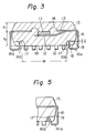
- FIG. 2 is a side view of
- Fig. 3 is a sectional view of
- Fig. 4 is a plan view of an embodiment of the present invention.
- the same portions are denoted by the same reference numerals.
- the tips 16b of the external leads 16 are formed perpendicular to or aslant (explained later) the main surface 18, the external leads 16 are not likely to be deformed due to an accidentally imposed slight pressure exerted by the upper part of the package and thus the standoff distance SO is not lost even when the middle portions 16a are soldered onto a mother board, such as a printed board.
- the standoff distance SO is the distance between the main surface 18 of the package and the mother board (not shown) when the device is mounted and plays an important role in radiating the heat of the semiconductor device. Without the tips 16b, the middle portions 16a tend to bend toward the main surface 18, and the predetermined standoff distance SO is not maintained.
- the resin 15 is divided into a portion above the internal leads and a portion below the internal leads, as is shown in Fig. 3, the upper portion having a thickness h and the lower portion having a thickness h 2 and the relationship h 1 ⁇ h 2 (for example, h 2 is 1.5 times as great as h I ) being maintained. Therefore, when the resin is molded, a greater amount of stress is accumulated in the lower portion than in the upper portion due to thermal contraction in the lower portion, with the result that the package undergoes deformation.
Abstract
Description
- The present invention relates to a semiconductor device including a main body moulded from plastics material and more particularly to an improvement in the construction of a leaded chip carrier package.
- In such semiconductor devices, an integrated circuit chip which is a circuit element is mounted on the chip-mounting portion of a lead frame which is formed as a unitary structure. The chip is connected to internal leads of the lead frame by wires, and a plastics resin is moulded around the chip, the wires, and the internal leads. A package of this type can be manufactured at a lower cost than can ceramic-type packages.
- In recent years, a variety of types of chip carriers have been proposed to meet the demand for the construction of smaller-sized packages. A ceramic-type chip carrier having no external leads is called a leadless chip carrier. A device having a body moulded from a plastics material having short external leads is called a resin-moulded or leaded chip carrier and has an advantage in cost over the ceramic type of chip carrier. Both the ceramic-type chip carrier and the resin-moulded type of chip carrier are constructed so that they are small in size and both are mounted on a printed circuit board by a simple soldering operation, it being unnecessary to insert the external leads into holes in the printed board, as is necessary in the case of conventional dual in-line package.
- In the conventional resin moulded type leaded chip carriers, the leads which are flat and provided on the base of the package, are soldered on conductor patterns of a printed circuit board lying in a flat plane beneath the package, with the result that the following drawbacks are created:
- 1. Whether soldering is complete or not can not be distinguished from the exterior of the package.
- 2. When there is a projection on the printed circuit board beneath the package the leads of the chip carrier can not completely contact the conductor patterns of the printed circuit board, with the result that soldering of the chip carrier and the printed circuit board can not be carried out.
- 3. The mechanical strength of the connection between the leads and the conductor patterns by the solder is weak.
- 4. The leads can not completely absorb differences in the heat expansion coefficient between the printed board and the chip carrier, with the result that an undesirable stress is created on the leads.
- A chip carrier assembly having a standoff distance and having the objective of eliminating the above- mentioned drawbacks was disclosed in IEEE Transactions On Components, Hybrids, and Manufacturing Technology, Vol CHMT-3,
No 4, December 1980, "Development of a 68-pin Multiple In-Line Package" by William L. Brodsky et al. This chip carrier assembly comprises a main body formed by moulding from a plastics material and a plurality of outer leads extending out of the main body, the main body having a base and a plurality of sides from which the outer leads extend, the main body including recesses and the outer leads being bent so that their tips are located in the recesses. However, this chip carrier assembly - has the following drawbacks:
- 1. The manufacturing process, particularly the lead bending operation, is not easy.
- 2. The flux used in the soldering operation remains in the recessed portions of the package.
- 3. The soldering state between the leads and the board can not be visually examined from the exterior of the package.
- 4. When the number of leads is increased in accordance with the development of a high density integrated-circuit device, the adjacent leads often short-circuit if they are deformed, and a standoff distance between the mother board and the lower surface of the package is not maintained.
- According to this invention we overcome these drawbacks by forming the recesses as channels opening to the sides and to the base, middle portions of the outer leads being spaced away from the base so that a predetermined standoff distance is maintained between them.
- The present invention provides a device in which short-circuiting between the adjacent external leads is prevented,and a standoff distance between the semiconductor device and its circuit board is maintained. Also the bending operation on the external leads can be readily carried out during its manufacturing process and an easy visual inspection of the soldered condition of the leads after it is soldered onto a printed circuit board can be carried out. Further the present invention provides a semiconductor device of the resin-moulded leaded chip carrier type which is capable of ensuring contacts between its leads and the conductor patterns of a printed circuit board during the soldering operation despite a deformation in either the chip carrier or the board.
- Particular examples of the present invention will now be described and contrasted with the prior art with reference to the accompanying drawings; in which:-
- Figure 1 is a partially sectioned side elevation of a prior art resin-moulded semiconductor device;
- Figure 2 is a side elevation of a first example of a resin-moulded semiconductor device in accordance with the present invention;
- Figure 3 is a cross-section through the first example of resin-moulded semiconductor device;
- Figure 4 is a plan of the first example;
- Figure 5 is a partially sectioned elevation of a second example;
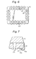
- Figure 6 is a plan of a third example; and,
- Figure 7 is a partially sectioned elevation of the third example.
- Figure 1 is a partial sectional view of the conventional resin-molded semiconductor device of the type as disclosed in the article mentioned above and which has the drawbacks previously mentioned. In Fig. 1, reference numeral 1 denotes an internal lead, 2 denotes an external lead, 3a and 3b, respectively, denote a middle portion and an end portion of the
external lead hollow portion 6 is formed so as to open only on themain surface 4, it becomes difficult to bend theend portion 3b of theexternal lead 2 in the final bending step due to the presence of the projecting portion 7. - Below is described a resin-molded semiconductor device of the leaded chip carrier type according to an embodiment of the present inventon, in connection with Figs. 2 to 4.
- Figure 2 is a side view of, Fig. 3 is a sectional view of, and Fig. 4 is a plan view of an embodiment of the present invention. In these drawings, the same portions are denoted by the same reference numerals.
- In the semiconductor device of this embodiment, a chip 11, which is a circuit element, is attached to a chip-mounting portion of a
lead frame 12. The chip 11 is connected tointernal leads 13 viawires 14, and aresin 15 is molded around the chip 11, thewires 14, thelead frame 12, and the internal leads 13.Grooves 17 are'formed in the corner portions defined by themain surface 18 and theside surfaces 19 of the package. Eachgroove 17 opens at both themain surface 18 and one of theside surfaces 19.Grooves 17 are spaced apart with a predetermined distance from each other and respectively correspond toexternal leads 16, which are so folded that theirtips 16b are positioned in thegrooves 17 and theirmiddle portions 16a are located on themain surface 18, with the result that a predetermined standoff distance SO is maintained. - In this embodiment, since the
tips 16b of theexternal leads 16 are positioned in thegrooves 17, theexternal leads 16 are not deformed sidewards and do not come into contact with each other. - Further, since the
tips 16b of theexternal leads 16 are formed perpendicular to or aslant (explained later) themain surface 18, theexternal leads 16 are not likely to be deformed due to an accidentally imposed slight pressure exerted by the upper part of the package and thus the standoff distance SO is not lost even when themiddle portions 16a are soldered onto a mother board, such as a printed board. The standoff distance SO is the distance between themain surface 18 of the package and the mother board (not shown) when the device is mounted and plays an important role in radiating the heat of the semiconductor device. Without thetips 16b, themiddle portions 16a tend to bend toward themain surface 18, and the predetermined standoff distance SO is not maintained. - According to this embodiment of the present invetnion, the
tips 16b, which have a length H, come into contact with the walls of thegrooves 17 and function as support rods even when themiddle portions 16a are inclined to deform toward themain surface 18. Therefore, theexternal leads 16 are not easily deformed. - On the other hand, the outer leads may be intentionally deformed slightly by depressing the package on a printed circuit board before soldering process to ensure the entire contacts between the outer leads and the conductor patterns of the printed circuit boards. This operation provides a practical advantage when the package or the board is undesirably warped.
- Furthermore, according to this embodiment, there is a small gap G between the ends of the
tips 16b and the walls of thegrooves 17, and there is a standoff SO between themain surface 18 and themiddle portions 16a so that theexternal leads 16 are allowed to turn with their root portions as centers. Therefore, even when stress is generated due to thermal expansion and contraction of the printed circuit board or thermal expansion and contraction of theresin 15 of the package after the device has been soldered onto the board, theexternal leads 16, which are resilient, absorb the stress. Namely, the device mounted on the printed circuit board via themiddle portions 16a can withstand changes in external temperature. - In a chip carrier package having leads, in general, the
resin 15 is divided into a portion above the internal leads and a portion below the internal leads, as is shown in Fig. 3, the upper portion having a thickness h and the lower portion having a thickness h2 and the relationship h1 < h2 (for example, h2 is 1.5 times as great as hI) being maintained. Therefore, when the resin is molded, a greater amount of stress is accumulated in the lower portion than in the upper portion due to thermal contraction in the lower portion, with the result that the package undergoes deformation. - In the embodiment of the present invention, however, since a plurality of
grooves 17 are formed in the corner portions defined by themain surface 18 and the side surfaces 19, the substantial width of the lower portion of resin is as denoted by W in Fig. 3, and the stress is reduced correspondingly. Accordingly, the imbalance in stress accumulated in the upper portion of resin and in the lower portion of resin is reduced, and the package is prevented from being deformed. - After the soldering process for mounting the device onto a printed circuit board which may be conducted in the conventional manner, the flux used in the process can be easily rinsed out and the soldered condition can be visually inspected because the soldered portions are exposed at side openings of the grooves.
- Figure 5 is a sectional view illustrating a portion of another embodiment of the present invention. In this embodiment, the ends of the
tips 16b of the external leads 16 are folded toward the direction of the bottom end corners 17' of thegrooves 17 opposite to the side surfaces 19. When pressure is exerted from the exterior, the ends of thetips 16b come into contact with the corners 17' so that their positions are fixed. Therefore, the external leads 16 are not bent undesirably. - In either case, the
tips 16b and themiddle portions 16a of the external leads 16 are located apart from the main body of the package. The process for bending the outer leads may be conducted as follows: the external leads 16 are first folded from the side of thetips 16b, and the boundary portion between the internal leads 13 and the external leads 16 is then folded. According to the present invention, thegrooves 17 are formed not only in themain surface 18 but also in the side surfaces 19. Accordingly, thetips 16b of the external leads 16 can be easily folded without any obstructions, as is shown in Fig. 1. - Figure 6 is a plan view of another embodiment of the present invention. In Fig. 6, grooves are formed between projecting
portions 22 or between the projectingportions 22 and 22'. This embodiment coresponds to a case in which the embodiment of Fig. 4 is modified so that a portion 20 (Fig. 4) is formed not at the main surface level but at the bottom level of thegrooves 17. Figure 7 is a partial sectional view of Fig..6. In the embodiment shown in Figs. 6 and 7, the same function and result as that in the embodiment shown in Figs. 3 to 5 can be obtained, except that the grooves defined by theprojection portions 22 do not have any bottom corner portion 17' as in Fig. 5 to stop thetips 16b when pressure is imposed onto the package downwardly. - According to the semiconductor device of the present invention as described above, short-circuiting does not occur between the external leads, the standoff distance is not lost due to deformation of the external leads, the device is not deformed due to thermal contraction, less stress builds up due to thermal expansion, and operability is not lost in the outer lead folding step. After the device is mounted on a printed circuit board by soldering, the flux used can be easily rinsed out and the soldered condition can be easily examined by a visual inspection.
Claims (4)
Applications Claiming Priority (2)
| Application Number | Priority Date | Filing Date | Title |
|---|---|---|---|
| JP57052061A JPS58169948A (en) | 1982-03-30 | 1982-03-30 | Resin-sealed type semiconductor device |
| JP52061/82 | 1982-03-30 |
Publications (3)
| Publication Number | Publication Date |
|---|---|
| EP0090608A2 true EP0090608A2 (en) | 1983-10-05 |
| EP0090608A3 EP0090608A3 (en) | 1985-05-22 |
| EP0090608B1 EP0090608B1 (en) | 1988-07-27 |
Family
ID=12904293
Family Applications (1)
| Application Number | Title | Priority Date | Filing Date |
|---|---|---|---|
| EP83301667A Expired EP0090608B1 (en) | 1982-03-30 | 1983-03-24 | Semiconductor device with moulded package |
Country Status (5)
| Country | Link |
|---|---|
| US (1) | US4698660A (en) |
| EP (1) | EP0090608B1 (en) |
| JP (1) | JPS58169948A (en) |
| DE (1) | DE3377553D1 (en) |
| IE (1) | IE54671B1 (en) |
Cited By (6)
| Publication number | Priority date | Publication date | Assignee | Title |
|---|---|---|---|---|
| EP0098051A2 (en) * | 1982-05-31 | 1984-01-11 | Kabushiki Kaisha Toshiba | A plastics-encapsulated circuit element |
| DE3421539A1 (en) * | 1984-06-08 | 1985-12-19 | Siemens AG, 1000 Berlin und 8000 München | Semiconductor component for SMD technology |
| EP0212521A1 (en) * | 1985-08-10 | 1987-03-04 | Fujitsu Limited | Package for integrated circuit |
| EP0261324A1 (en) * | 1986-09-26 | 1988-03-30 | Texas Instruments Incorporated | Plastic package for large chip size integrated circuit |
| EP0439825A2 (en) * | 1990-01-29 | 1991-08-07 | Motorola Inc. | Semiconductor package having leads that break-away from supports |
| EP3193406A4 (en) * | 2014-09-11 | 2018-08-15 | NSK Ltd. | Multipolar lead component, and connection device for substrate |
Families Citing this family (20)
| Publication number | Priority date | Publication date | Assignee | Title |
|---|---|---|---|---|
| JPS61225841A (en) * | 1985-03-30 | 1986-10-07 | Toshiba Corp | Resin-sealed semiconductor device |
| JPS625642U (en) * | 1985-06-27 | 1987-01-14 | ||
| JPS628645U (en) * | 1985-06-28 | 1987-01-19 | ||
| JPS6212959U (en) * | 1985-07-06 | 1987-01-26 | ||
| JPH0642345Y2 (en) * | 1986-03-12 | 1994-11-02 | ロ−ム株式会社 | Semiconductor device |
| US5150193A (en) * | 1987-05-27 | 1992-09-22 | Hitachi, Ltd. | Resin-encapsulated semiconductor device having a particular mounting structure |
| US4872260A (en) * | 1988-01-19 | 1989-10-10 | Gte Products Corporation | Method of making pre-formed lead-ins for an IC package |
| US4890154A (en) * | 1988-03-02 | 1989-12-26 | Lsi Logic Corporation | Semiconductor package profile |
| US4829669A (en) * | 1988-04-28 | 1989-05-16 | Nec Corporation | Method of manufacturing a chip carrier |
| JP2507053B2 (en) * | 1989-06-14 | 1996-06-12 | 松下電子工業株式会社 | J-lead package type semiconductor device |
| US4967262A (en) * | 1989-11-06 | 1990-10-30 | Micron Technology, Inc. | Gull-wing zig-zag inline lead package having end-of-package anchoring pins |
| JPH05144992A (en) * | 1991-11-18 | 1993-06-11 | Mitsubishi Electric Corp | Semiconductor device and its production, lead frame used for semiconductor production and its production |
| MY114547A (en) * | 1992-05-25 | 2002-11-30 | Hitachi Ltd | Thin type semiconductor device, module structure using the device and method of mounting the device on board |
| WO1997044821A1 (en) * | 1996-05-22 | 1997-11-27 | Olin Corporation | Metal electronic package with peripherally attached leads |
| JP2924854B2 (en) * | 1997-05-20 | 1999-07-26 | 日本電気株式会社 | Semiconductor device and manufacturing method thereof |
| US5986894A (en) * | 1997-09-29 | 1999-11-16 | Pulse Engineering, Inc. | Microelectronic component carrier and method of its manufacture |
| JP4644008B2 (en) * | 2005-03-09 | 2011-03-02 | 三菱電機株式会社 | Semiconductor module |
| DE102014100110A1 (en) * | 2014-01-07 | 2015-07-09 | Infineon Technologies Ag | Package with connection pins with lateral reversal point and laterally exposed free end |
| CN105514057B (en) * | 2016-01-15 | 2017-03-29 | 气派科技股份有限公司 | High-density integrated circuit package structure and integrated circuit |
| CN111082306B (en) * | 2019-11-13 | 2021-10-22 | 海南师范大学 | Semiconductor laser array and packaging method thereof |
Citations (3)
| Publication number | Priority date | Publication date | Assignee | Title |
|---|---|---|---|---|
| FR2360174A1 (en) * | 1976-07-30 | 1978-02-24 | Amp Inc | INTEGRATED CIRCUIT BOX AND ITS MANUFACTURING PROCESS |
| US4195193A (en) * | 1979-02-23 | 1980-03-25 | Amp Incorporated | Lead frame and chip carrier housing |
| FR2456390A1 (en) * | 1979-05-11 | 1980-12-05 | Thomson Csf | Connector grid for integrated circuit encapsulation - forms external contacts and internal links from single piece component |
Family Cites Families (6)
| Publication number | Priority date | Publication date | Assignee | Title |
|---|---|---|---|---|
| US3877064A (en) * | 1974-02-22 | 1975-04-08 | Amp Inc | Device for connecting leadless integrated circuit packages to a printed-circuit board |
| US4142287A (en) * | 1976-12-27 | 1979-03-06 | Amp Incorporated | Electrical devices such as watches and method of construction thereof |
| JPS5498168U (en) * | 1977-12-21 | 1979-07-11 | ||
| US4224637A (en) * | 1978-08-10 | 1980-09-23 | Minnesota Mining And Manufacturing Company | Leaded mounting and connector unit for an electronic device |
| JPS57155758A (en) * | 1981-03-23 | 1982-09-25 | Hitachi Ltd | Semiconductor device |
| US4463217A (en) * | 1981-09-14 | 1984-07-31 | Texas Instruments Incorporated | Plastic surface mounted high pinout integrated circuit package |
-
1982
- 1982-03-30 JP JP57052061A patent/JPS58169948A/en active Granted
-
1983
- 1983-03-24 EP EP83301667A patent/EP0090608B1/en not_active Expired
- 1983-03-24 DE DE8383301667T patent/DE3377553D1/en not_active Expired
- 1983-03-30 IE IE718/83A patent/IE54671B1/en not_active IP Right Cessation
-
1986
- 1986-02-12 US US06/833,535 patent/US4698660A/en not_active Expired - Fee Related
Patent Citations (3)
| Publication number | Priority date | Publication date | Assignee | Title |
|---|---|---|---|---|
| FR2360174A1 (en) * | 1976-07-30 | 1978-02-24 | Amp Inc | INTEGRATED CIRCUIT BOX AND ITS MANUFACTURING PROCESS |
| US4195193A (en) * | 1979-02-23 | 1980-03-25 | Amp Incorporated | Lead frame and chip carrier housing |
| FR2456390A1 (en) * | 1979-05-11 | 1980-12-05 | Thomson Csf | Connector grid for integrated circuit encapsulation - forms external contacts and internal links from single piece component |
Non-Patent Citations (1)
| Title |
|---|
| PATENTS ABSTRACTS OF JAPAN, Vol.6 No. 259 (E-149) (1137) December 1982. & JP-A-57 155 758 (Hitachi Seisakusho K.K.) 25-09-1982 * |
Cited By (9)
| Publication number | Priority date | Publication date | Assignee | Title |
|---|---|---|---|---|
| EP0098051A2 (en) * | 1982-05-31 | 1984-01-11 | Kabushiki Kaisha Toshiba | A plastics-encapsulated circuit element |
| EP0098051B1 (en) * | 1982-05-31 | 1990-01-31 | Kabushiki Kaisha Toshiba | A plastics-encapsulated circuit element |
| DE3421539A1 (en) * | 1984-06-08 | 1985-12-19 | Siemens AG, 1000 Berlin und 8000 München | Semiconductor component for SMD technology |
| EP0212521A1 (en) * | 1985-08-10 | 1987-03-04 | Fujitsu Limited | Package for integrated circuit |
| US4724280A (en) * | 1985-08-10 | 1988-02-09 | Fujitsu Limited | Package for integrated circuit |
| EP0261324A1 (en) * | 1986-09-26 | 1988-03-30 | Texas Instruments Incorporated | Plastic package for large chip size integrated circuit |
| EP0439825A2 (en) * | 1990-01-29 | 1991-08-07 | Motorola Inc. | Semiconductor package having leads that break-away from supports |
| EP0439825A3 (en) * | 1990-01-29 | 1991-09-11 | Motorola Inc. | Semiconductor package having leads that break-away from supports |
| EP3193406A4 (en) * | 2014-09-11 | 2018-08-15 | NSK Ltd. | Multipolar lead component, and connection device for substrate |
Also Published As
| Publication number | Publication date |
|---|---|
| EP0090608B1 (en) | 1988-07-27 |
| JPS634950B2 (en) | 1988-02-01 |
| EP0090608A3 (en) | 1985-05-22 |
| IE830718L (en) | 1983-09-30 |
| US4698660A (en) | 1987-10-06 |
| IE54671B1 (en) | 1990-01-03 |
| DE3377553D1 (en) | 1988-09-01 |
| JPS58169948A (en) | 1983-10-06 |
Similar Documents
| Publication | Publication Date | Title |
|---|---|---|
| EP0090608B1 (en) | Semiconductor device with moulded package | |
| US4465898A (en) | Carrier for integrated circuit | |
| US5413970A (en) | Process for manufacturing a semiconductor package having two rows of interdigitated leads | |
| US4496965A (en) | Stacked interdigitated lead frame assembly | |
| KR100242994B1 (en) | Buttom lead frame and buttom lead frame for the use | |
| US4463217A (en) | Plastic surface mounted high pinout integrated circuit package | |
| US5777382A (en) | Plastic packaging for a surface mounted integrated circuit | |
| EP0155044A2 (en) | Plastic pin grid array chip carrier | |
| EP0228869A2 (en) | Method of manufacturing an electronic component package | |
| JPH06125021A (en) | Surface-mount type diode | |
| KR19980032479A (en) | Surface installation TO-220 package and its manufacturing process | |
| US5349235A (en) | High density vertically mounted semiconductor package | |
| US5728601A (en) | Process for manufacturing a single in-line package for surface mounting | |
| US4272140A (en) | Arrangement for mounting dual-in-line packaged integrated circuits to thick/thin film circuits | |
| KR100407751B1 (en) | Semiconductor device | |
| JPS6225262B2 (en) | ||
| US4530552A (en) | Electrical connector for integrated circuit package | |
| US4495376A (en) | Carrier for integrated circuit | |
| US5849609A (en) | Semiconductor package and a method of manufacturing thereof | |
| KR930004255B1 (en) | Resin sealed semiconductor device | |
| JPS60254646A (en) | Semiconductor device | |
| JP2507852B2 (en) | Semiconductor device | |
| KR19980054997A (en) | Stacked Semiconductor Packages | |
| KR100235498B1 (en) | Semiconductor package | |
| JPS6013186Y2 (en) | electrical connectors |
Legal Events
| Date | Code | Title | Description |
|---|---|---|---|
| PUAI | Public reference made under article 153(3) epc to a published international application that has entered the european phase |
Free format text: ORIGINAL CODE: 0009012 |
|
| AK | Designated contracting states |
Designated state(s): DE FR GB |
|
| PUAL | Search report despatched |
Free format text: ORIGINAL CODE: 0009013 |
|
| AK | Designated contracting states |
Designated state(s): DE FR GB |
|
| 17P | Request for examination filed |
Effective date: 19851115 |
|
| 17Q | First examination report despatched |
Effective date: 19870330 |
|
| GRAA | (expected) grant |
Free format text: ORIGINAL CODE: 0009210 |
|
| AK | Designated contracting states |
Kind code of ref document: B1 Designated state(s): DE FR GB |
|
| REF | Corresponds to: |
Ref document number: 3377553 Country of ref document: DE Date of ref document: 19880901 |
|
| ET | Fr: translation filed | ||
| PLBI | Opposition filed |
Free format text: ORIGINAL CODE: 0009260 |
|
| 26 | Opposition filed |
Opponent name: TELEFUNKEN ELECTRONIC GMBH Effective date: 19890424 Opponent name: DEUTSCHE ITT INDUSTRIES GMBH Effective date: 19890426 |
|
| PLBN | Opposition rejected |
Free format text: ORIGINAL CODE: 0009273 |
|
| STAA | Information on the status of an ep patent application or granted ep patent |
Free format text: STATUS: OPPOSITION REJECTED |
|
| 27O | Opposition rejected |
Effective date: 19910422 |
|
| PGFP | Annual fee paid to national office [announced via postgrant information from national office to epo] |
Ref country code: GB Payment date: 19930312 Year of fee payment: 11 |
|
| PGFP | Annual fee paid to national office [announced via postgrant information from national office to epo] |
Ref country code: FR Payment date: 19930330 Year of fee payment: 11 |
|
| PGFP | Annual fee paid to national office [announced via postgrant information from national office to epo] |
Ref country code: DE Payment date: 19930521 Year of fee payment: 11 |
|
| PG25 | Lapsed in a contracting state [announced via postgrant information from national office to epo] |
Ref country code: GB Effective date: 19940324 |
|
| GBPC | Gb: european patent ceased through non-payment of renewal fee |
Effective date: 19940324 |
|
| PG25 | Lapsed in a contracting state [announced via postgrant information from national office to epo] |
Ref country code: FR Effective date: 19941130 |
|
| PG25 | Lapsed in a contracting state [announced via postgrant information from national office to epo] |
Ref country code: DE Effective date: 19941201 |
|
| REG | Reference to a national code |
Ref country code: FR Ref legal event code: ST |