EP0091775A2 - A method of manufacturing a semiconductor device comprising an interconnection layer - Google Patents
A method of manufacturing a semiconductor device comprising an interconnection layer Download PDFInfo
- Publication number
- EP0091775A2 EP0091775A2 EP83301920A EP83301920A EP0091775A2 EP 0091775 A2 EP0091775 A2 EP 0091775A2 EP 83301920 A EP83301920 A EP 83301920A EP 83301920 A EP83301920 A EP 83301920A EP 0091775 A2 EP0091775 A2 EP 0091775A2
- Authority
- EP
- European Patent Office
- Prior art keywords
- metal
- layer
- silicon
- region
- interconnection
- Prior art date
- Legal status (The legal status is an assumption and is not a legal conclusion. Google has not performed a legal analysis and makes no representation as to the accuracy of the status listed.)
- Granted
Links
Images


Classifications
-
- H—ELECTRICITY
- H01—ELECTRIC ELEMENTS
- H01L—SEMICONDUCTOR DEVICES NOT COVERED BY CLASS H10
- H01L23/00—Details of semiconductor or other solid state devices
- H01L23/52—Arrangements for conducting electric current within the device in operation from one component to another, i.e. interconnections, e.g. wires, lead frames
- H01L23/535—Arrangements for conducting electric current within the device in operation from one component to another, i.e. interconnections, e.g. wires, lead frames including internal interconnections, e.g. cross-under constructions
-
- H—ELECTRICITY
- H01—ELECTRIC ELEMENTS
- H01L—SEMICONDUCTOR DEVICES NOT COVERED BY CLASS H10
- H01L21/00—Processes or apparatus adapted for the manufacture or treatment of semiconductor or solid state devices or of parts thereof
- H01L21/70—Manufacture or treatment of devices consisting of a plurality of solid state components formed in or on a common substrate or of parts thereof; Manufacture of integrated circuit devices or of parts thereof
- H01L21/71—Manufacture of specific parts of devices defined in group H01L21/70
- H01L21/768—Applying interconnections to be used for carrying current between separate components within a device comprising conductors and dielectrics
- H01L21/76838—Applying interconnections to be used for carrying current between separate components within a device comprising conductors and dielectrics characterised by the formation and the after-treatment of the conductors
- H01L21/76886—Modifying permanently or temporarily the pattern or the conductivity of conductive members, e.g. formation of alloys, reduction of contact resistances
- H01L21/76889—Modifying permanently or temporarily the pattern or the conductivity of conductive members, e.g. formation of alloys, reduction of contact resistances by forming silicides of refractory metals
-
- H—ELECTRICITY
- H01—ELECTRIC ELEMENTS
- H01L—SEMICONDUCTOR DEVICES NOT COVERED BY CLASS H10
- H01L21/00—Processes or apparatus adapted for the manufacture or treatment of semiconductor or solid state devices or of parts thereof
- H01L21/70—Manufacture or treatment of devices consisting of a plurality of solid state components formed in or on a common substrate or of parts thereof; Manufacture of integrated circuit devices or of parts thereof
- H01L21/71—Manufacture of specific parts of devices defined in group H01L21/70
- H01L21/768—Applying interconnections to be used for carrying current between separate components within a device comprising conductors and dielectrics
- H01L21/76838—Applying interconnections to be used for carrying current between separate components within a device comprising conductors and dielectrics characterised by the formation and the after-treatment of the conductors
- H01L21/76895—Local interconnects; Local pads, as exemplified by patent document EP0896365
-
- H—ELECTRICITY
- H01—ELECTRIC ELEMENTS
- H01L—SEMICONDUCTOR DEVICES NOT COVERED BY CLASS H10
- H01L23/00—Details of semiconductor or other solid state devices
- H01L23/52—Arrangements for conducting electric current within the device in operation from one component to another, i.e. interconnections, e.g. wires, lead frames
- H01L23/522—Arrangements for conducting electric current within the device in operation from one component to another, i.e. interconnections, e.g. wires, lead frames including external interconnections consisting of a multilayer structure of conductive and insulating layers inseparably formed on the semiconductor body
- H01L23/532—Arrangements for conducting electric current within the device in operation from one component to another, i.e. interconnections, e.g. wires, lead frames including external interconnections consisting of a multilayer structure of conductive and insulating layers inseparably formed on the semiconductor body characterised by the materials
- H01L23/53204—Conductive materials
- H01L23/53271—Conductive materials containing semiconductor material, e.g. polysilicon
-
- H—ELECTRICITY
- H01—ELECTRIC ELEMENTS
- H01L—SEMICONDUCTOR DEVICES NOT COVERED BY CLASS H10
- H01L2924/00—Indexing scheme for arrangements or methods for connecting or disconnecting semiconductor or solid-state bodies as covered by H01L24/00
- H01L2924/0001—Technical content checked by a classifier
- H01L2924/0002—Not covered by any one of groups H01L24/00, H01L24/00 and H01L2224/00
-
- Y—GENERAL TAGGING OF NEW TECHNOLOGICAL DEVELOPMENTS; GENERAL TAGGING OF CROSS-SECTIONAL TECHNOLOGIES SPANNING OVER SEVERAL SECTIONS OF THE IPC; TECHNICAL SUBJECTS COVERED BY FORMER USPC CROSS-REFERENCE ART COLLECTIONS [XRACs] AND DIGESTS
- Y10—TECHNICAL SUBJECTS COVERED BY FORMER USPC
- Y10S—TECHNICAL SUBJECTS COVERED BY FORMER USPC CROSS-REFERENCE ART COLLECTIONS [XRACs] AND DIGESTS
- Y10S438/00—Semiconductor device manufacturing: process
- Y10S438/98—Utilizing process equivalents or options
Definitions
- the present invention relates to a method of manufacturing a semiconductor device and, more particularly, to an improvement in a method for connecting a diffusion interconnection region to an interconnection layer in an MOS type device.
- Fig. 1A is a plan view showing part of an LSI having a direct contact portion.
- a gate electrode 101 and an interconnection layer 102, both of which are formed of poly-silicon, are disposed on a silicon substrate 100.
- Reference numerals 103 and 104 designate diffusion interconnection regions, which are, respectively, source and drain regions of an MOS transistor.
- a circuit equivalent to the device shown in Fig. 1A is indicated in Fig. 1B.
- the electrical connection between the layer 102 and the region 104 is performed in a direct contact portion 105 by a direct contact method.
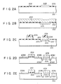
- Figs. 2A to 2D are sectional views along A-A in Fig. lA, showing schematic manufacturing steps of the device in Fig. lA.
- an oxide film 202 which becomes a gate oxide film is formed, for example, to a thickness of approx. 200A by thermal oxidation on a p-type silicon substrate 201.
- a predetermined resist pattern (not shown) as a mask, a direct contact region 203 of the thermal oxide film 202 is selectively etched and removed, for example, with NH 4 F, and the surface of the silicon substrate of the portion is exposed (Fig. 2A).
- a poly-silicon layer 204 is formed on the overall surface by a CVD (chemical vapor deposition) method, and is heat treated in a POC1 3 atmosphere, thereby diffusing phosphorus in the layer 204.
- the phosphorus is diffused in the substrate 201 in the direct contact region, and a diffusion region 205 which will become a direct contact portion is formed (Fig. 2B).
- a photoresist pattern 206 is formed to cover those portions of the poly-silicon layer 204 which will become a gate electrode and an interconnection layer, and the layer 204 is removed by etching using the layer 206 as a mask.
- This etching may be performed with a reactive ion etching which employs an etchant, e.g., CCE 4 .
- the etching stops on the surface of the film 202 in the transistor portion, but does not reach the substrate 201.
- a groove 207 is formed in the silicon substrate as shown in Fig. 2C.
- the portion of the film 202 which is not covered with the layer 204 is removed by etching to expose the substrate 201; thereafter an impurity, e.g., As is ion implanted in a dose of 3 to 4 x 1015 cm-2 at an accelerating voltage of 50 kV, and is heat treated, for example, at 1,000°C for approx. 30 min., thereby forming a source region 208a, a drain region 208b and a diffusion interconnection region 208c of an extension of the drain region 208b, all of which are n +- regions (Fig. 2D).
- the impurity is injected to the inner surface of the groove 207, an n + diffusion region 208d is formed in this portion, thereby electrically connecting a poly-silicon layer 209 to the region 208c.
- the depth and the shape of the groove are not constant, but largely vary depending upon the conditions of etching and the time of an overetching. Therefore, the resistance value of the region 208d in this groove portion becomes remarkably irregular.
- the groove 207 is largely formed, for example, in a circular sectional shape as shown in Fig. 2E, a diffusion region is not formed in the side walls of the groove 207, resulting in an electric isolation between the layer 209 and the layer 208c.
- Such a problem becomes an important problem as a junction depth becomes shallow upon microminiaturization of the device, causing a remarkable decrease in the yield of the LSI.
- a crystal defect produced in the vicinity of the groove 207 by the reactive ion etching causes an increase in the junction leakage in the diffusion layer, resulting in a problem such as a decrease in the performance of the device.
- CMOS Complementary MOS
- a source region 308a, a drain region 308b and a diffusion interconnection region 308c of an extension of the region 308b are p +- type diffusion layers formed, for example, by boron ion implantation.
- a direct contact portion 305 is an n +- type diffusion region (when steps similar to those in Figs. 2A to 2D are employed), and a p-n junction is not formed between an n +- type direct contact portion 305 and an n-type silicon substrate 301, and the portion 305 and the substrate 301' will shortcircuit.
- a gate electrode 310 made of an n +- type poly-silicon is initially formed, for example as shown in Fig. 3B, then a source region 308a, a drain region 308b and a diffusion interconnection region 308c made of a p +- type diffusion layer and thereafter an n +- type polysilicon layer 309 are formed, and then an n-type direct contact portion 311 are formed by a diffusion of an impurity from the layer 309, a p-n junction is formed between the portion 311 and the region 308c, and an ohmic contact is not formed.
- a method of manufacturing a semiconductor device which comprises the steps of forming an interconnection layer through an insulating film on a semiconductor substrate, and connecting the diffusion interconnection region in the surface portion of said substrate to said interconnection layer by growing a metal or metal semiconductor compound on the surface of said substrate and the interconnection layer.
- the thickness of the insulating film is preferably 50 to 1,500A, and the thickness of the grown metal or metal semiconductor compound layer is 300 to 2,000A.
- a method of growing the metal or metal semiconductor compound includes, for example, a method of alloying the silicon by the steps of depositing the metal film on the overall surface and annealing the metal, and a method using a metal vapor atmosphere for this growing.
- both p-type and n-type poly-silicon interconnection layers can be connected to both diffusion interconnection regions of n-channel transistor and p-channel transistors, thereby increasing the degree of freedom of designing the LSI.
- the metal or metal semiconductor compound is selectively grown, the direct contact of the diffusion interconnection region and the interconnection layer is possible. Therefore, the integration can be significantly increased as compared with the method of connecting the two by forming the contact hole in the insulating film and forming the metal member therein.
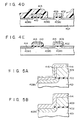
- Figs. 4A to 4E show an embodiment in which the method of the present invention is applied to the connection of the diffusion interconnection region and the interconnection layer in an MOS transistor.
- an oxide film 402 having, for example, 50 to 1,500A, e.g., 100A is formed by thermal oxidation, for example, on a p-type silicon substrate 401, and a poly-silicon is then deposited and patterned on the overall surface, thereby forming a gate electrode 410 and an interconnection layer 409.
- These electrodes 410 and 409 are formed of poly-silicon which includes an impurity such as phosphorus or arsenic.
- the impurity may be introduced into the poly-silicon layer when it is deposited or it may be doped in the poly-silicon layer by a heat treatment, for example, in POCi 3 or an ion implantation of phosphorus or arsenic, after the formation of the poly-silicon layer. Or, an impurity may be doped simultaneously with the later formation of source and drain regions.
- arsenic is, for example, ion implanted at an accelerating voltage of 50 kV in a dose of 3 to 5 x 10 15 cm- 2 , thereby forming a source region 408a, a drain region 408b and a diffusion interconnection region 408c. This ion implantation may be performed through the film 402, or may be performed after its removal.
- a thick field insulating film is formed. Subsequently, a heat treatment is conducted in an oxidation atmosphere or N 2 atmosphere having, for example, a temperature of 1,000°C, thereby activating the ion implanted arsenic.
- Si0 2 is deposited by a CVD method on the overall surface, thereby forming an Si0 2 film 411.
- the film 411 may be formed by thermal oxidation.
- the film 411 is etched by an anisotropic etching such as a reactive ion etching using an etchant, e.g., a gas mixture of CF 4 and H 2 , thereby exposing the regions 408a, 408b and 408c, and Si0 2 films 412a and 412b are retained on the side walls of the electrode 410 and the layer 409, respectively (Fig. 4C).
- a photoresist film 413 is coated on the region excluding the layer 409 and its periphery. Then, the film 412b of the side wall of the layer 409 is removed by etching such as, for example, with NH 4 F (Fig. 4D). After the removal of the film 413, a Pt film is formed by a vacuum evaporation to a thickness of approx. 500 A, and is annealed, for example, at 550°C for approx. 15 min., and a PtSi (platinum silicide) layer 414 is formed on the portion where the Pt film and the silicon or poly-silicon are contacted.
- a PtSi platinum silicide
- the layer 414 is formed on a source region 408a, a drain region 408b and diffusion interconnection region 408c, on a gate electrode 410, and on upper and side surfaces of the layer 409, but is not formed on the Si0 2 film 412a.
- the continuous PtSi film 414 is formed to a thickness of, for example, about 1,OOOA, on the upper and side surfaces of the layer 409 and on the diffusion regions 408b, 408c, thereby connecting the layer 409 and the region 408c.
- Figs. 5A and 5B show enlarged views of the connecting portion
- Fig. 5A shows the intermediate state of formation of the PtSi layer 414
- Fig. 5B shows the finished state of the forming reaction of the PtSi.
- the layer 409 and the region 408c are not directly connected due to the intermediary of the oxide film 402, but are-connected through the layer 414 formed on the respective surfaces.
- the Si0 2 film 412b on the side wall of the layer 409 is removed, but it is not necessary to remove all of the film 412b. As shown in Fig. 6, it is sufficient to remove only the connecting portion to the region 408c. As shown in Fig. 6, part of the film 412 is removed, and the other part is retained, thereby preventing the field oxide layer from becoming thin.
- Fig. 4E corresponds to the sectional view along the line B-B in Fig. 6. In the embodiment described above, the S10 2 film 412b is retained on the side walls of the layer 409 as shown in Fig. 4C, and thereafter is removed by etching as shown in Fig. 4D. However, the present invention is not limited to this embodiment.
- That portion of the Si0 2 film on the upper and side surfaces of the layer 409 and its periphery is etched off using a photoresist film as a mask, and then the residual Si0 2 film is subjected to RIE (reactive ion etching) to be retained on the side wall of the electrode 410.
- RIE reactive ion etching
- the method according to the present invention does not comprise the step of removing the oxide film by etching before forming the poly- silicon layer at the connecting portion between the interconnecting layer and the diffusion interconnection region. Therefore, when the poly-silicon layer is etched, due to the presence of the oxide film, the formation of the groove and the etching of the substrate are prevented, unlike in the conventional method. Therefore, the problem that the resistance in the direct ' contact portion will vary according to the overetching time of the poly-silicon and that the contact cannot be formed can be eliminated. Further, since the substrate is not exposed, the problem that the leak current of the p-n junction increases due to the crystal defects produced in the substrate in the reactive ion etching step can also be eliminated.
- the interconnection layer and the substrate are insulated via the oxide film, even if the p +- type poly-silicon is, for example, used instead of the n +- type poly- silicon, no shortcircuit occurs between the interconnection layer and the substrate as in the conventional device.
- the electrode 410 and the layer 409 are simultaneously formed by patterning of the poly-silicon layer.
- the present invention is not limited to this embodiment.
- a gate electrode 701 made of poly-silicon is initially formed, then arsenic is ion implanted into the substrate 701 to form a source region 708a, a drain region 708b and a diffusion interconnection region 708c of the extension of the drain region 708b, thereafter an interconnection layer 709 made of poly-silicon is formed through an oxide film 716, and then steps similar to those shown in Figs. 4B to 4E may be performed.
- the layer 709 is p-type, a p-n junction is not formed between the layer 709 and the n-type interconnection region 708c due to the presence of the film 716. Further, since the PtSi and the n +- type and p +- type silicon form an ohmic contact, the layer 709 and the region 708c will always form an ohmic contact.
- the gate electrode and the interconnection layer are formed of poly- silicon.
- the poly-silicon it is also possible for them to be formed of a so-called "polycide", i.e., a two-layer structure of poly-silicon and a metal silicide. Even in the case of the polycide, it is possible to form another metal silicide layer on top of the metal silicide layer of the upper layer in the step shown in Fig. 4E.
- the PtSi layer is formed by thermal annealing.
- the present invention is not limited to this, but the metal or metal semiconductor compound may be grown by various methods. The growing method of the metal or metal semiconductor compound including the case of forming the PtSi layer by thermal annealing will now be described.
- a metal is deposited on the entire surface of a silicon wafer and thermal annealing is performed.
- the metal silicide is produced only at positions where the metal and silicon come in contact.
- a metal silicide film is formed on the source region, the drain region, the diffusion interconnection region and the interconnection layer and may be formed on the upper surface of the gate electrode.
- the metal which is deposited on the field oxide film and the side walls of the gate electrode may easily be eliminated by, for example, an acid treatment.
- Metals such as W, Pd, Pt, Ni, Mo, Nb, Ta, Ir, and Ti which react with silicon to produce a stable silicide film may be used. Pt is easy to use for this purpose.
- Formation of the metal silicide film may be performed by irradiation by a laser beam after the metal is deposited, instead of by thermal annealing.
- the silicon region may be scanned with the laser beam once at an output of about 10 W by using a CW-Ar laser so that the same results as in annealing described above may be obtained.
- the method in which the laser beam is used has advantages in that the temperature of the wafer is not made high. Further, when the laser beam is used, it may be selectively radiated on only predetermined spots so that the metal silicide film may be selectively formed.
- the insulating material on the side faces of the gate electrode prevents thermal conduction between the desired metal silicide layer and the gate electrode.
- the metal silicide layer may be formed by ion-implanting an impurity, for example Ar, at an interface of the metal layer with the silicon or into the silicon substrate after the metal is deposited. This method is called "ion beam mixing". According to this method, even if a thin oxide film (at a thickness of, for example, 10 to 20A) or contaminant such as carbon derived from a vacuum pumping system remains on the surface of the silicon wafer before the metal is deposited, the stable metal silicide layer is easily formed by reacting the metal and the silicon.
- an impurity for example Ar
- the yield of the wafers increases by about 10 to 20 % as compared with a method according to thermal annealing.
- the impurity here is not limited to Ar, and other impurities such as As, Si and Xe may be used.
- the ion beam mixing method does not necessarily require a heating process, in the MIS semiconductor device which is produced in a proportional-reduced scale, a shallow low resistance layer may be formed.
- the metal silicide layer and simultaneously the source, drain and diffusion interconnection regions are formed by using an impurity of opposite conductivity type to that of the silicon substrate.
- ions with larger masses such as Si, Ar and Xe may be implanted with boron to enhance the ion beam mixing effect.
- Pd when Pd is used as the metal, more PdSi is formed than Pd 2 Si. Therefore, this method has an advantage in that the silicide layer is formed having a resistivity which is 2/3 to 1/2 the resistivity of the silicide layer obtained by thermal annealing.
- the silicidation reaction may be promoted and the thickness of the metal silicide layer may be increased.
- Thermal annealing, CW laser beam irradiation, CW electron beam irradiation or the like may be used for annealing in this stage. Since the annealing after the ion beam mixing and after or before the removal of the unreacted metal film is effective towards improvement of crystallizability of metal silicide and lowering of resistivity of the diffusion regions, it is desirable to perform such annealing.
- the wafer is heated at a temperature above 200°C, while a metal halide gas, or a mixture of a metal halide gas and a reducing gas are introduced, so that a metal layer is selectively formed on the exposed silicon region only.
- a metal such as W, Pd, Pt, Ni, Mo, Nb, Ta, Ti, or other metals which may be deposited on the silicon layer by the halide reduction may be used for the metal here.
- W or Mo may be deposited on the silicon layer by using a gas of WF 6 or HoF 6 , or a gas mixture of WF 6 or MoF 6 and H 2 .
- Fig. 8 shows a sectional view of an MOS transistor produced by placing a substrate at 200 to 600°C in a gas mixture of WF 6 and H 2 , thereby forming a W layer selectively only on the surfaces of the silicon and the poly- silicon.
- This structure is similar to that in Fig. 4E except that the metal silicide is not formed by the reaction of the metal and the silicon in the section of the MOS transistor.
- Reference numeral 800 shows the W layer thus formed.
- the insulating film which is formed on. the side walls of the gate electrode may be eliminated and an impurity of opposite conductivity type to that of the silicon substrate may be ion-implanted.
- the doping of the impurity into source region, the drain region, the diffusion interconnection region and the interconnection layer may thus be formed.
- oil of a vacuum pump is ionized by accelerated ions so that the oil ions become attached to the surface of the silicon substrate to form a carbon film.
- the carbon film is not sufficiently eliminated in a cleaning process and formation of the metal or metal silicide layer may be impaired.
- the impurity is ion-implanted after the metal or metal silicide layer is formed as described above, the problem described above is eliminated.
Abstract
Description
- The present invention relates to a method of manufacturing a semiconductor device and, more particularly, to an improvement in a method for connecting a diffusion interconnection region to an interconnection layer in an MOS type device.
- Heretofore, in an LSI (large-scale integrated circuit), an interconnection between elements has been carried out with a diffusion layer, a polysilicon layer and an aluminum layer. The connections between these interconnection layers, e.g., the connection between a diffusion layer and a polysilicon layer, has been performed by a so-called direct contact method which is also known as buried contact. However, the conventional connecting method employing the direct contact method has various problems. These will now be described with reference to the drawings.
- Fig. 1A is a plan view showing part of an LSI having a direct contact portion. A
gate electrode 101 and aninterconnection layer 102, both of which are formed of poly-silicon, are disposed on a silicon substrate 100.Reference numerals layer 102 and theregion 104 is performed in adirect contact portion 105 by a direct contact method. - Figs. 2A to 2D are sectional views along A-A in Fig. lA, showing schematic manufacturing steps of the device in Fig. lA. For example, an
oxide film 202 which becomes a gate oxide film is formed, for example, to a thickness of approx. 200A by thermal oxidation on a p-type silicon substrate 201. Subsequently, with a predetermined resist pattern (not shown) as a mask, adirect contact region 203 of thethermal oxide film 202 is selectively etched and removed, for example, with NH4F, and the surface of the silicon substrate of the portion is exposed (Fig. 2A). - Then, a poly-
silicon layer 204 is formed on the overall surface by a CVD (chemical vapor deposition) method, and is heat treated in a POC13 atmosphere, thereby diffusing phosphorus in thelayer 204. At this time, the phosphorus is diffused in thesubstrate 201 in the direct contact region, and adiffusion region 205 which will become a direct contact portion is formed (Fig. 2B). - Subsequently, a
photoresist pattern 206 is formed to cover those portions of the poly-silicon layer 204 which will become a gate electrode and an interconnection layer, and thelayer 204 is removed by etching using thelayer 206 as a mask. This etching may be performed with a reactive ion etching which employs an etchant, e.g., CCE4. The etching stops on the surface of thefilm 202 in the transistor portion, but does not reach thesubstrate 201. However, since there is not oxide film in the direct contact portion, agroove 207 is formed in the silicon substrate as shown in Fig. 2C. - Then, the portion of the
film 202 which is not covered with thelayer 204 is removed by etching to expose thesubstrate 201; thereafter an impurity, e.g., As is ion implanted in a dose of 3 to 4 x 1015 cm-2 at an accelerating voltage of 50 kV, and is heat treated, for example, at 1,000°C for approx. 30 min., thereby forming a source region 208a, adrain region 208b and a diffusion interconnection region 208c of an extension of thedrain region 208b, all of which are n+-regions (Fig. 2D). At this time, the impurity is injected to the inner surface of thegroove 207, an n+ diffusion region 208d is formed in this portion, thereby electrically connecting a poly-silicon layer 209 to the region 208c. - According to the above-described method, however, the depth and the shape of the groove are not constant, but largely vary depending upon the conditions of etching and the time of an overetching. Therefore, the resistance value of the
region 208d in this groove portion becomes remarkably irregular. When thegroove 207 is largely formed, for example, in a circular sectional shape as shown in Fig. 2E, a diffusion region is not formed in the side walls of thegroove 207, resulting in an electric isolation between thelayer 209 and the layer 208c. Such a problem becomes an important problem as a junction depth becomes shallow upon microminiaturization of the device, causing a remarkable decrease in the yield of the LSI. Further, a crystal defect produced in the vicinity of thegroove 207 by the reactive ion etching causes an increase in the junction leakage in the diffusion layer, resulting in a problem such as a decrease in the performance of the device. - The foregoing description relates to the case of an n-channel MOS transistor formed on the p-type silicon substrate. The following important problem exists in a so-called CMOS (Complementary MOS) circuit in which a p-channel MOS transistor and an n-channel MOS transistor are formed on the same substrate. In the portion of the p-channel transistor when an n+-type is used as a poly- silicon layer, as shown, for example, in Fig. 3A, a
source region 308a, adrain region 308b and a diffusion interconnection region 308c of an extension of theregion 308b are p+-type diffusion layers formed, for example, by boron ion implantation. However, adirect contact portion 305 is an n+-type diffusion region (when steps similar to those in Figs. 2A to 2D are employed), and a p-n junction is not formed between an n+-typedirect contact portion 305 and an n-type silicon substrate 301, and theportion 305 and the substrate 301' will shortcircuit. - When only a
gate electrode 310 made of an n+-type poly-silicon is initially formed, for example as shown in Fig. 3B, then asource region 308a, adrain region 308b and a diffusion interconnection region 308c made of a p+-type diffusion layer and thereafter an n+-type polysilicon layer 309 are formed, and then an n-typedirect contact portion 311 are formed by a diffusion of an impurity from thelayer 309, a p-n junction is formed between theportion 311 and the region 308c, and an ohmic contact is not formed. - Thus, when an interconnection layer made of n+-type poly-silicon is used in the MOS circuit, the diffusion interconnection region and the poly-silicon layer could not be connected by the direct contact method in the p-channel MOS transistor. On the contrary, even when the interconnection layer made of a p+-type poly-silicon is used, similar problems exist in the direct contact portion of the n-channel MOS transistor. These problems have caused a significant restriction in the design of the circuit.
- It is an object of the present invention to provide a method of manufacturing a semiconductor device which comprises connecting a diffusion interconnection region with an interconnection layer by a direct contact method and which is capable of increasing the integration of the device, the yiled, and the degree of design freedom.
- According to an aspect of the present invention, there is provided a method of manufacturing a semiconductor device which comprises the steps of forming an interconnection layer through an insulating film on a semiconductor substrate, and connecting the diffusion interconnection region in the surface portion of said substrate to said interconnection layer by growing a metal or metal semiconductor compound on the surface of said substrate and the interconnection layer.
- In the method of the present invention, the thickness of the insulating film is preferably 50 to 1,500A, and the thickness of the grown metal or metal semiconductor compound layer is 300 to 2,000A.
- A method of growing the metal or metal semiconductor compound includes, for example, a method of alloying the silicon by the steps of depositing the metal film on the overall surface and annealing the metal, and a method using a metal vapor atmosphere for this growing.
- According to the method of the present invention, it is possible to perform the connection of the diffusion interconnection region to the interconnection layer with a high yield. When the method of the present invention is applied, for example, to the manufacture of a CMOS device, both p-type and n-type poly-silicon interconnection layers can be connected to both diffusion interconnection regions of n-channel transistor and p-channel transistors, thereby increasing the degree of freedom of designing the LSI. Further, when the metal or metal semiconductor compound is selectively grown, the direct contact of the diffusion interconnection region and the interconnection layer is possible. Therefore, the integration can be significantly increased as compared with the method of connecting the two by forming the contact hole in the insulating film and forming the metal member therein.
- The present invention is best understood by reference to the accompanying drawings of which:
- Fig. 1A is a sectional view showing an MOS transistor for describing a conventional direct contact method;
- Fig. 1B is a circuit diagram of the device in Fig. lA;
- Figs. 2A to 2E are sectional views showing the steps of the conventional direct contact method;
- Figs. 3A and 3B are sectional views showing defects of the conventional direct contact method in the CMOS;
- Figs. 4A to 4E are sectional views showing the steps of manufacturing an n-channel MOS LSI according to the present invention;
- Figs. 5A and 5B are enlarged views of the connection portion of the diffusion interconnection region and the interconnection layer in Fig. 4E;
- Fig. 6 is a plan view of Fig. 4E;
- Fig. 7 is a sectional view of the MOS transistor obtained according to another embodiment of the present invention; and
- Fig. 8 is a sectional view of the MOS transistor obtained according to still another embodiment of the present invention.
- The embodiments of the present invention will now be described in more detail with reference to the accompanying drawings.
- Figs. 4A to 4E show an embodiment in which the method of the present invention is applied to the connection of the diffusion interconnection region and the interconnection layer in an MOS transistor.
- As shown in Fig. 4A, an
oxide film 402 having, for example, 50 to 1,500A, e.g., 100A is formed by thermal oxidation, for example, on a p-type silicon substrate 401, and a poly-silicon is then deposited and patterned on the overall surface, thereby forming agate electrode 410 and aninterconnection layer 409. Theseelectrodes source region 408a, adrain region 408b and adiffusion interconnection region 408c. This ion implantation may be performed through thefilm 402, or may be performed after its removal. In the field region (the region around the region shown in Fig. 4A), a thick field insulating film is formed. Subsequently, a heat treatment is conducted in an oxidation atmosphere or N2 atmosphere having, for example, a temperature of 1,000°C, thereby activating the ion implanted arsenic. - Then, as shown in Fig. 4B, Si02 is deposited by a CVD method on the overall surface, thereby forming an Si02 film 411. The
film 411 may be formed by thermal oxidation. Thereafter, thefilm 411 is etched by an anisotropic etching such as a reactive ion etching using an etchant, e.g., a gas mixture of CF4 and H2, thereby exposing theregions electrode 410 and thelayer 409, respectively (Fig. 4C). - Subsequently, a
photoresist film 413 is coated on the region excluding thelayer 409 and its periphery. Then, thefilm 412b of the side wall of thelayer 409 is removed by etching such as, for example, with NH4F (Fig. 4D). After the removal of thefilm 413, a Pt film is formed by a vacuum evaporation to a thickness of approx. 500 A, and is annealed, for example, at 550°C for approx. 15 min., and a PtSi (platinum silicide)layer 414 is formed on the portion where the Pt film and the silicon or poly-silicon are contacted. Subsequently, the unreacted Pt film is removed with aqua regia, thereby obtaining a structure shown in Fig. 4E. Thelayer 414 is formed on asource region 408a, adrain region 408b anddiffusion interconnection region 408c, on agate electrode 410, and on upper and side surfaces of thelayer 409, but is not formed on the Si02 film 412a. Thus, thecontinuous PtSi film 414 is formed to a thickness of, for example, about 1,OOOA, on the upper and side surfaces of thelayer 409 and on thediffusion regions layer 409 and theregion 408c. - Figs. 5A and 5B show enlarged views of the connecting portion, Fig. 5A shows the intermediate state of formation of the
PtSi layer 414, and Fig. 5B shows the finished state of the forming reaction of the PtSi. As evident from Fig. 5B, thelayer 409 and theregion 408c are not directly connected due to the intermediary of theoxide film 402, but are-connected through thelayer 414 formed on the respective surfaces. - In the step shown in Fig. 4D, the Si02 film 412b on the side wall of the
layer 409 is removed, but it is not necessary to remove all of thefilm 412b. As shown in Fig. 6, it is sufficient to remove only the connecting portion to theregion 408c. As shown in Fig. 6, part of thefilm 412 is removed, and the other part is retained, thereby preventing the field oxide layer from becoming thin. Fig. 4E corresponds to the sectional view along the line B-B in Fig. 6. In the embodiment described above, the S102 film 412b is retained on the side walls of thelayer 409 as shown in Fig. 4C, and thereafter is removed by etching as shown in Fig. 4D. However, the present invention is not limited to this embodiment. For example, that portion of the Si02 film on the upper and side surfaces of thelayer 409 and its periphery is etched off using a photoresist film as a mask, and then the residual Si02 film is subjected to RIE (reactive ion etching) to be retained on the side wall of theelectrode 410. - The method according to the present invention, as described above, does not comprise the step of removing the oxide film by etching before forming the poly- silicon layer at the connecting portion between the interconnecting layer and the diffusion interconnection region. Therefore, when the poly-silicon layer is etched, due to the presence of the oxide film, the formation of the groove and the etching of the substrate are prevented, unlike in the conventional method. Therefore, the problem that the resistance in the direct ' contact portion will vary according to the overetching time of the poly-silicon and that the contact cannot be formed can be eliminated. Further, since the substrate is not exposed, the problem that the leak current of the p-n junction increases due to the crystal defects produced in the substrate in the reactive ion etching step can also be eliminated. Moreover, since the interconnection layer and the substrate are insulated via the oxide film, even if the p+-type poly-silicon is, for example, used instead of the n+-type poly- silicon, no shortcircuit occurs between the interconnection layer and the substrate as in the conventional device.
- In the embodiment described above, the
electrode 410 and thelayer 409 are simultaneously formed by patterning of the poly-silicon layer. However, the present invention is not limited to this embodiment. For example, as shown in Fig. 7, agate electrode 701 made of poly-silicon is initially formed, then arsenic is ion implanted into thesubstrate 701 to form a source region 708a, adrain region 708b and a diffusion interconnection region 708c of the extension of thedrain region 708b, thereafter an interconnection layer 709 made of poly-silicon is formed through an oxide film 716, and then steps similar to those shown in Figs. 4B to 4E may be performed. In this case, even if the layer 709 is p-type, a p-n junction is not formed between the layer 709 and the n-type interconnection region 708c due to the presence of the film 716. Further, since the PtSi and the n+-type and p+-type silicon form an ohmic contact, the layer 709 and the region 708c will always form an ohmic contact. - In the embodiments described above, the case of the p-type substrate has been described. However, the present invention is not limited to this. In the case of an n-type substrate, or even in the case of a CMOS circuit which includes both the p-type and the n-type, the present invention can be applied similarly. In the embodiments described above, the gate electrode and the interconnection layer are formed of poly- silicon. However, instead of the poly-silicon it is also possible for them to be formed of a so-called "polycide", i.e., a two-layer structure of poly-silicon and a metal silicide. Even in the case of the polycide, it is possible to form another metal silicide layer on top of the metal silicide layer of the upper layer in the step shown in Fig. 4E.
- In the embodiments described above, the PtSi layer is formed by thermal annealing. However, the present invention is not limited to this, but the metal or metal semiconductor compound may be grown by various methods. The growing method of the metal or metal semiconductor compound including the case of forming the PtSi layer by thermal annealing will now be described.
- A metal is deposited on the entire surface of a silicon wafer and thermal annealing is performed. The metal silicide is produced only at positions where the metal and silicon come in contact. As a result, a metal silicide film is formed on the source region, the drain region, the diffusion interconnection region and the interconnection layer and may be formed on the upper surface of the gate electrode. The metal which is deposited on the field oxide film and the side walls of the gate electrode may easily be eliminated by, for example, an acid treatment. Metals such as W, Pd, Pt, Ni, Mo, Nb, Ta, Ir, and Ti which react with silicon to produce a stable silicide film may be used. Pt is easy to use for this purpose.
- Formation of the metal silicide film may be performed by irradiation by a laser beam after the metal is deposited, instead of by thermal annealing. For example, after the metal is deposited, the silicon region may be scanned with the laser beam once at an output of about 10 W by using a CW-Ar laser so that the same results as in annealing described above may be obtained. The method in which the laser beam is used has advantages in that the temperature of the wafer is not made high. Further, when the laser beam is used, it may be selectively radiated on only predetermined spots so that the metal silicide film may be selectively formed. In this case, the insulating material on the side faces of the gate electrode prevents thermal conduction between the desired metal silicide layer and the gate electrode. The same effect may be obtained when a CW electron beam is used instead of the laser beam. Further, the metal silicide layer may be formed by ion-implanting an impurity, for example Ar, at an interface of the metal layer with the silicon or into the silicon substrate after the metal is deposited. This method is called "ion beam mixing". According to this method, even if a thin oxide film (at a thickness of, for example, 10 to 20A) or contaminant such as carbon derived from a vacuum pumping system remains on the surface of the silicon wafer before the metal is deposited, the stable metal silicide layer is easily formed by reacting the metal and the silicon. Therefore, problems such as nonuniform formation of the metal silicide layer due to the presence of the thin oxide film or contaminant, high contact resistance between the metal silicide layer and the silicon layer, and the like are eliminated. Therefore, the yield of the wafers increases by about 10 to 20 % as compared with a method according to thermal annealing. The impurity here is not limited to Ar, and other impurities such as As, Si and Xe may be used. Furthermore, since the ion beam mixing method does not necessarily require a heating process, in the MIS semiconductor device which is produced in a proportional-reduced scale, a shallow low resistance layer may be formed. According to the ion beam mixing method, the metal silicide layer and simultaneously the source, drain and diffusion interconnection regions are formed by using an impurity of opposite conductivity type to that of the silicon substrate. For forming P+-source, drain and diffusion interconnection regions, ions with larger masses such as Si, Ar and Xe may be implanted with boron to enhance the ion beam mixing effect. In addition to this, when Pd is used as the metal, more PdSi is formed than Pd2Si. Therefore, this method has an advantage in that the silicide layer is formed having a resistivity which is 2/3 to 1/2 the resistivity of the silicide layer obtained by thermal annealing. By performing the annealing after the ion beam mixing is performed and before the unreacted metal film is eliminated, the silicidation reaction may be promoted and the thickness of the metal silicide layer may be increased. Thermal annealing, CW laser beam irradiation, CW electron beam irradiation or the like may be used for annealing in this stage. Since the annealing after the ion beam mixing and after or before the removal of the unreacted metal film is effective towards improvement of crystallizability of metal silicide and lowering of resistivity of the diffusion regions, it is desirable to perform such annealing.
- Formation of the metal film on the silicon region on which the insulating film is not formed will be described. The wafer is heated at a temperature above 200°C, while a metal halide gas, or a mixture of a metal halide gas and a reducing gas are introduced, so that a metal layer is selectively formed on the exposed silicon region only. A metal such as W, Pd, Pt, Ni, Mo, Nb, Ta, Ti, or other metals which may be deposited on the silicon layer by the halide reduction may be used for the metal here. For example, W or Mo may be deposited on the silicon layer by using a gas of WF6 or HoF6, or a gas mixture of WF6 or MoF6 and H2.
- Fig. 8 shows a sectional view of an MOS transistor produced by placing a substrate at 200 to 600°C in a gas mixture of WF6 and H2, thereby forming a W layer selectively only on the surfaces of the silicon and the poly- silicon. This structure is similar to that in Fig. 4E except that the metal silicide is not formed by the reaction of the metal and the silicon in the section of the MOS transistor.
Reference numeral 800 shows the W layer thus formed. - After the metal film or metal silicide film is formed on the silicon region which is exposed and on which the insulating film is not formed, the insulating film which is formed on. the side walls of the gate electrode may be eliminated and an impurity of opposite conductivity type to that of the silicon substrate may be ion-implanted. The doping of the impurity into source region, the drain region, the diffusion interconnection region and the interconnection layer may thus be formed. In the method in which the metal or metal silicide layer is formed after the impurity is ion-implanted, oil of a vacuum pump is ionized by accelerated ions so that the oil ions become attached to the surface of the silicon substrate to form a carbon film. The carbon film is not sufficiently eliminated in a cleaning process and formation of the metal or metal silicide layer may be impaired. However, in the method in which the impurity is ion-implanted after the metal or metal silicide layer is formed as described above, the problem described above is eliminated.
Claims (10)
Applications Claiming Priority (2)
| Application Number | Priority Date | Filing Date | Title |
|---|---|---|---|
| JP57240/82 | 1982-04-08 | ||
| JP57057240A JPS58175846A (en) | 1982-04-08 | 1982-04-08 | Manufacture of semicondutor device |
Publications (3)
| Publication Number | Publication Date |
|---|---|
| EP0091775A2 true EP0091775A2 (en) | 1983-10-19 |
| EP0091775A3 EP0091775A3 (en) | 1985-07-03 |
| EP0091775B1 EP0091775B1 (en) | 1988-06-22 |
Family
ID=13050004
Family Applications (1)
| Application Number | Title | Priority Date | Filing Date |
|---|---|---|---|
| EP83301920A Expired EP0091775B1 (en) | 1982-04-08 | 1983-04-06 | A method of manufacturing a semiconductor device comprising an interconnection layer |
Country Status (4)
| Country | Link |
|---|---|
| US (1) | US4528744A (en) |
| EP (1) | EP0091775B1 (en) |
| JP (1) | JPS58175846A (en) |
| DE (1) | DE3377178D1 (en) |
Cited By (7)
| Publication number | Priority date | Publication date | Assignee | Title |
|---|---|---|---|---|
| US4488348A (en) * | 1983-06-15 | 1984-12-18 | Hewlett-Packard Company | Method for making a self-aligned vertically stacked gate MOS device |
| EP0200364A1 (en) * | 1985-03-29 | 1986-11-05 | Advanced Micro Devices, Inc. | Method of fabricating metal silicide gate electrodes and interconnections |
| EP0206481A2 (en) * | 1985-05-07 | 1986-12-30 | Hitachi, Ltd. | Semiconductor device having a multi-layered wiring |
| GB2177255A (en) * | 1985-06-28 | 1987-01-14 | Northern Telecom Ltd | VLSI MOSFET circuits using refractory metal and/or refractory metal silicide |
| US4855247A (en) * | 1988-01-19 | 1989-08-08 | Standard Microsystems Corporation | Process for fabricating self-aligned silicide lightly doped drain MOS devices |
| EP0463458A1 (en) * | 1990-06-28 | 1992-01-02 | International Business Machines Corporation | Method and structure for interconnecting different polysilicon zones on semiconductor substrates for integrated circuits |
| US5612243A (en) * | 1989-07-10 | 1997-03-18 | Texas Instruments Incorporated | Polycide local interconnect method and structure |
Families Citing this family (34)
| Publication number | Priority date | Publication date | Assignee | Title |
|---|---|---|---|---|
| JPH0618213B2 (en) * | 1982-06-25 | 1994-03-09 | 松下電子工業株式会社 | Method for manufacturing semiconductor device |
| IT1213120B (en) * | 1984-01-10 | 1989-12-14 | Ates Componenti Elettron | PROCESS FOR THE MANUFACTURE OF COMPLEMENTARY LOW VOLTAGE THRESHOLD MOS TRANSISTORS IN HIGH DENSITY INTEGRATED CIRCUITS AND RESULTING STRUCTURE. |
| US4727038A (en) * | 1984-08-22 | 1988-02-23 | Mitsubishi Denki Kabushiki Kaisha | Method of fabricating semiconductor device |
| GB2164491B (en) * | 1984-09-14 | 1988-04-07 | Stc Plc | Semiconductor devices |
| JPS61139058A (en) * | 1984-12-11 | 1986-06-26 | Seiko Epson Corp | Production apparatus for semiconductor |
| US5190886A (en) * | 1984-12-11 | 1993-03-02 | Seiko Epson Corporation | Semiconductor device and method of production |
| US4743564A (en) * | 1984-12-28 | 1988-05-10 | Kabushiki Kaisha Toshiba | Method for manufacturing a complementary MOS type semiconductor device |
| DE3683679D1 (en) * | 1985-04-26 | 1992-03-12 | Fujitsu Ltd | METHOD FOR PRODUCING A CONTACT ARRANGEMENT FOR A SEMICONDUCTOR ARRANGEMENT. |
| US4630357A (en) * | 1985-08-02 | 1986-12-23 | Ncr Corporation | Method for forming improved contacts between interconnect layers of an integrated circuit |
| US4703551A (en) * | 1986-01-24 | 1987-11-03 | Ncr Corporation | Process for forming LDD MOS/CMOS structures |
| US4753897A (en) * | 1986-03-14 | 1988-06-28 | Motorola Inc. | Method for providing contact separation in silicided devices using false gate |
| US4908688A (en) * | 1986-03-14 | 1990-03-13 | Motorola, Inc. | Means and method for providing contact separation in silicided devices |
| KR910002831B1 (en) * | 1986-04-23 | 1991-05-06 | 아메리칸 텔리폰 앤드 텔레그라프 캄파니 | Process for manufacturing semiconductor devices |
| US4825271A (en) * | 1986-05-20 | 1989-04-25 | Kabushiki Kaisha Toshiba | Nonvolatile semiconductor memory |
| JPS632535U (en) * | 1986-06-20 | 1988-01-09 | ||
| GB2199694A (en) * | 1986-12-23 | 1988-07-13 | Philips Electronic Associated | A method of manufacturing a semiconductor device |
| US4735680A (en) * | 1986-11-17 | 1988-04-05 | Yen Yung Chau | Method for the self-aligned silicide formation in IC fabrication |
| GB2214708A (en) * | 1988-01-20 | 1989-09-06 | Philips Nv | A method of manufacturing a semiconductor device |
| US4902379A (en) * | 1988-02-08 | 1990-02-20 | Eastman Kodak Company | UHV compatible lift-off method for patterning nobel metal silicide |
| US5041394A (en) * | 1989-09-11 | 1991-08-20 | Texas Instruments Incorporated | Method for forming protective barrier on silicided regions |
| US4988643A (en) * | 1989-10-10 | 1991-01-29 | Vlsi Technology, Inc. | Self-aligning metal interconnect fabrication |
| US5010030A (en) * | 1989-10-30 | 1991-04-23 | Motorola, Inc. | Semiconductor process using selective deposition |
| US5070029A (en) * | 1989-10-30 | 1991-12-03 | Motorola, Inc. | Semiconductor process using selective deposition |
| JP2632620B2 (en) * | 1992-01-14 | 1997-07-23 | 大岡技研株式会社 | Gear products |
| US5306951A (en) * | 1992-05-14 | 1994-04-26 | Micron Technology, Inc. | Sidewall silicidation for improved reliability and conductivity |
| US5529941A (en) * | 1994-03-28 | 1996-06-25 | Vlsi Technology, Inc. | Method for making an integrated circuit structure |
| US5585299A (en) * | 1996-03-19 | 1996-12-17 | United Microelectronics Corporation | Process for fabricating a semiconductor electrostatic discharge (ESD) protective device |
| JPH10112531A (en) * | 1996-08-13 | 1998-04-28 | Hitachi Ltd | Manufacture of semiconductor integrated circuit device |
| US6335280B1 (en) * | 1997-01-13 | 2002-01-01 | Asm America, Inc. | Tungsten silicide deposition process |
| TW396646B (en) * | 1997-09-11 | 2000-07-01 | Lg Semicon Co Ltd | Manufacturing method of semiconductor devices |
| KR100344818B1 (en) * | 1997-09-24 | 2002-11-18 | 주식회사 하이닉스반도체 | Semiconductor device and method for manufacturing the same |
| US6208004B1 (en) * | 1998-08-19 | 2001-03-27 | Philips Semiconductor, Inc. | Semiconductor device with high-temperature-stable gate electrode for sub-micron applications and fabrication thereof |
| US20050060933A1 (en) * | 2003-08-22 | 2005-03-24 | Henson David Lee | Horticultural container lining for enhancing contained soil's water absorption |
| US7504329B2 (en) * | 2005-05-11 | 2009-03-17 | Interuniversitair Microelektronica Centrum (Imec) | Method of forming a Yb-doped Ni full silicidation low work function gate electrode for n-MOSFET |
Citations (2)
| Publication number | Priority date | Publication date | Assignee | Title |
|---|---|---|---|---|
| DE3013559A1 (en) * | 1979-04-09 | 1980-10-16 | Tokyo Shibaura Electric Co | SEMICONDUCTOR DEVICE AND METHOD FOR THEIR PRODUCTION |
| EP0046371A1 (en) * | 1980-08-13 | 1982-02-24 | Fujitsu Limited | Method of manufacturing a semiconductor device |
Family Cites Families (6)
| Publication number | Priority date | Publication date | Assignee | Title |
|---|---|---|---|---|
| US4102733A (en) * | 1977-04-29 | 1978-07-25 | International Business Machines Corporation | Two and three mask process for IGFET fabrication |
| US4141022A (en) * | 1977-09-12 | 1979-02-20 | Signetics Corporation | Refractory metal contacts for IGFETS |
| US4277881A (en) * | 1978-05-26 | 1981-07-14 | Rockwell International Corporation | Process for fabrication of high density VLSI circuits, having self-aligned gates and contacts for FET devices and conducting lines |
| DE2926874A1 (en) * | 1979-07-03 | 1981-01-22 | Siemens Ag | METHOD FOR PRODUCING LOW-RESISTANT, DIFFUSED AREAS IN SILICON GATE TECHNOLOGY |
| US4305200A (en) * | 1979-11-06 | 1981-12-15 | Hewlett-Packard Company | Method of forming self-registering source, drain, and gate contacts for FET transistor structures |
| US4419809A (en) * | 1981-12-30 | 1983-12-13 | International Business Machines Corporation | Fabrication process of sub-micrometer channel length MOSFETs |
-
1982
- 1982-04-08 JP JP57057240A patent/JPS58175846A/en active Granted
-
1983
- 1983-04-05 US US06/482,229 patent/US4528744A/en not_active Expired - Lifetime
- 1983-04-06 DE DE8383301920T patent/DE3377178D1/en not_active Expired
- 1983-04-06 EP EP83301920A patent/EP0091775B1/en not_active Expired
Patent Citations (2)
| Publication number | Priority date | Publication date | Assignee | Title |
|---|---|---|---|---|
| DE3013559A1 (en) * | 1979-04-09 | 1980-10-16 | Tokyo Shibaura Electric Co | SEMICONDUCTOR DEVICE AND METHOD FOR THEIR PRODUCTION |
| EP0046371A1 (en) * | 1980-08-13 | 1982-02-24 | Fujitsu Limited | Method of manufacturing a semiconductor device |
Non-Patent Citations (1)
| Title |
|---|
| IBM TECHNICAL DISCLOSURE BULLETIN, Vol.23, No.6, November, 1980, pages 2563-2566, ARMONK, (US). V.L.RIDEOUT: "Method of fabricating MOSFET integrated circuits with low resistivity interconnection lines". * |
Cited By (9)
| Publication number | Priority date | Publication date | Assignee | Title |
|---|---|---|---|---|
| US4488348A (en) * | 1983-06-15 | 1984-12-18 | Hewlett-Packard Company | Method for making a self-aligned vertically stacked gate MOS device |
| EP0200364A1 (en) * | 1985-03-29 | 1986-11-05 | Advanced Micro Devices, Inc. | Method of fabricating metal silicide gate electrodes and interconnections |
| EP0206481A2 (en) * | 1985-05-07 | 1986-12-30 | Hitachi, Ltd. | Semiconductor device having a multi-layered wiring |
| EP0206481A3 (en) * | 1985-05-07 | 1987-08-26 | Hitachi, Ltd. | Semiconductor device having a multi-layered wiring |
| GB2177255A (en) * | 1985-06-28 | 1987-01-14 | Northern Telecom Ltd | VLSI MOSFET circuits using refractory metal and/or refractory metal silicide |
| GB2177255B (en) * | 1985-06-28 | 1989-04-26 | Northern Telecom Ltd | Vlsi mosfet circuits using refractory metal and/or refractory metal silicide |
| US4855247A (en) * | 1988-01-19 | 1989-08-08 | Standard Microsystems Corporation | Process for fabricating self-aligned silicide lightly doped drain MOS devices |
| US5612243A (en) * | 1989-07-10 | 1997-03-18 | Texas Instruments Incorporated | Polycide local interconnect method and structure |
| EP0463458A1 (en) * | 1990-06-28 | 1992-01-02 | International Business Machines Corporation | Method and structure for interconnecting different polysilicon zones on semiconductor substrates for integrated circuits |
Also Published As
| Publication number | Publication date |
|---|---|
| EP0091775B1 (en) | 1988-06-22 |
| JPS58175846A (en) | 1983-10-15 |
| JPH0343778B2 (en) | 1991-07-03 |
| EP0091775A3 (en) | 1985-07-03 |
| DE3377178D1 (en) | 1988-07-28 |
| US4528744A (en) | 1985-07-16 |
Similar Documents
| Publication | Publication Date | Title |
|---|---|---|
| US4528744A (en) | Method of manufacturing a semiconductor device | |
| US4609568A (en) | Self-aligned metal silicide process for integrated circuits having self-aligned polycrystalline silicon electrodes | |
| US4433468A (en) | Method for making semiconductor device having improved thermal stress characteristics | |
| US4914500A (en) | Method for fabricating semiconductor devices which include sources and drains having metal-containing material regions, and the resulting devices | |
| US4795718A (en) | Self-aligned contact for MOS processing | |
| JP2543948B2 (en) | Method for manufacturing semiconductor device | |
| US4769337A (en) | Method of forming selective polysilicon wiring layer to source, drain and emitter regions by implantation through polysilicon layer | |
| EP0054259A2 (en) | Method of manufacturing a semiconductor device of the MIS type | |
| JPH0578173B2 (en) | ||
| US5001081A (en) | Method of manufacturing a polysilicon emitter and a polysilicon gate using the same etch of polysilicon on a thin gate oxide | |
| EP0097918A1 (en) | Semiconductor device and method of making the same | |
| KR19990072393A (en) | Semiconductor Device and Method for Making the Same | |
| EP0732746B1 (en) | Method of manufacturing a complementary bipolar transistor integrated circuit | |
| US6228766B1 (en) | Process for fabricating semiconductor device without separation between silicide layer and insulating layer | |
| KR100206683B1 (en) | Method for forming protective barrier on silicided regions | |
| EP0763256B1 (en) | METHOD OF MANUFACTURING A SEMICONDUCTOR DEVICE WITH BiCMOS CIRCUIT | |
| US4274193A (en) | Method for making a closed gate MOS transistor with self-aligned contacts | |
| JP2948486B2 (en) | Method for manufacturing semiconductor device | |
| US3925105A (en) | Process for fabricating integrated circuits utilizing ion implantation | |
| JPH1131665A (en) | Manufacture of semiconductor integrated circuit | |
| JPH0127589B2 (en) | ||
| JPS61258447A (en) | Manufacture of semiconductor device | |
| JPS6138858B2 (en) | ||
| JPH0554263B2 (en) | ||
| KR100266029B1 (en) | Method for fabricating semiconductor device |
Legal Events
| Date | Code | Title | Description |
|---|---|---|---|
| PUAI | Public reference made under article 153(3) epc to a published international application that has entered the european phase |
Free format text: ORIGINAL CODE: 0009012 |
|
| 17P | Request for examination filed |
Effective date: 19830414 |
|
| AK | Designated contracting states |
Designated state(s): DE FR GB IT NL |
|
| RAP1 | Party data changed (applicant data changed or rights of an application transferred) |
Owner name: KABUSHIKI KAISHA TOSHIBA |
|
| PUAL | Search report despatched |
Free format text: ORIGINAL CODE: 0009013 |
|
| AK | Designated contracting states |
Designated state(s): DE FR GB IT NL |
|
| 17Q | First examination report despatched |
Effective date: 19861110 |
|
| GRAA | (expected) grant |
Free format text: ORIGINAL CODE: 0009210 |
|
| AK | Designated contracting states |
Kind code of ref document: B1 Designated state(s): DE FR GB |
|
| REF | Corresponds to: |
Ref document number: 3377178 Country of ref document: DE Date of ref document: 19880728 |
|
| ET | Fr: translation filed | ||
| PLBE | No opposition filed within time limit |
Free format text: ORIGINAL CODE: 0009261 |
|
| STAA | Information on the status of an ep patent application or granted ep patent |
Free format text: STATUS: NO OPPOSITION FILED WITHIN TIME LIMIT |
|
| 26N | No opposition filed | ||
| PGFP | Annual fee paid to national office [announced via postgrant information from national office to epo] |
Ref country code: GB Payment date: 19970401 Year of fee payment: 15 |
|
| PGFP | Annual fee paid to national office [announced via postgrant information from national office to epo] |
Ref country code: FR Payment date: 19970409 Year of fee payment: 15 |
|
| PGFP | Annual fee paid to national office [announced via postgrant information from national office to epo] |
Ref country code: DE Payment date: 19970414 Year of fee payment: 15 |
|
| PG25 | Lapsed in a contracting state [announced via postgrant information from national office to epo] |
Ref country code: GB Free format text: LAPSE BECAUSE OF NON-PAYMENT OF DUE FEES Effective date: 19980406 |
|
| PG25 | Lapsed in a contracting state [announced via postgrant information from national office to epo] |
Ref country code: FR Free format text: THE PATENT HAS BEEN ANNULLED BY A DECISION OF A NATIONAL AUTHORITY Effective date: 19980430 |
|
| GBPC | Gb: european patent ceased through non-payment of renewal fee |
Effective date: 19980406 |
|
| PG25 | Lapsed in a contracting state [announced via postgrant information from national office to epo] |
Ref country code: DE Free format text: LAPSE BECAUSE OF NON-PAYMENT OF DUE FEES Effective date: 19990202 |
|
| REG | Reference to a national code |
Ref country code: FR Ref legal event code: ST |