EP0093659A1 - Mounting for integrated circuit devices - Google Patents
Mounting for integrated circuit devices Download PDFInfo
- Publication number
- EP0093659A1 EP0093659A1 EP83400843A EP83400843A EP0093659A1 EP 0093659 A1 EP0093659 A1 EP 0093659A1 EP 83400843 A EP83400843 A EP 83400843A EP 83400843 A EP83400843 A EP 83400843A EP 0093659 A1 EP0093659 A1 EP 0093659A1
- Authority
- EP
- European Patent Office
- Prior art keywords
- face
- support
- network
- diffuser element
- integrated circuit
- Prior art date
- Legal status (The legal status is an assumption and is not a legal conclusion. Google has not performed a legal analysis and makes no representation as to the accuracy of the status listed.)
- Withdrawn
Links
Images
Classifications
-
- H—ELECTRICITY
- H01—ELECTRIC ELEMENTS
- H01L—SEMICONDUCTOR DEVICES NOT COVERED BY CLASS H10
- H01L23/00—Details of semiconductor or other solid state devices
- H01L23/34—Arrangements for cooling, heating, ventilating or temperature compensation ; Temperature sensing arrangements
- H01L23/36—Selection of materials, or shaping, to facilitate cooling or heating, e.g. heatsinks
- H01L23/373—Cooling facilitated by selection of materials for the device or materials for thermal expansion adaptation, e.g. carbon
- H01L23/3736—Metallic materials
-
- H—ELECTRICITY
- H01—ELECTRIC ELEMENTS
- H01L—SEMICONDUCTOR DEVICES NOT COVERED BY CLASS H10
- H01L23/00—Details of semiconductor or other solid state devices
- H01L23/34—Arrangements for cooling, heating, ventilating or temperature compensation ; Temperature sensing arrangements
- H01L23/36—Selection of materials, or shaping, to facilitate cooling or heating, e.g. heatsinks
-
- H—ELECTRICITY
- H01—ELECTRIC ELEMENTS
- H01L—SEMICONDUCTOR DEVICES NOT COVERED BY CLASS H10
- H01L24/00—Arrangements for connecting or disconnecting semiconductor or solid-state bodies; Methods or apparatus related thereto
- H01L24/01—Means for bonding being attached to, or being formed on, the surface to be connected, e.g. chip-to-package, die-attach, "first-level" interconnects; Manufacturing methods related thereto
- H01L24/42—Wire connectors; Manufacturing methods related thereto
- H01L24/47—Structure, shape, material or disposition of the wire connectors after the connecting process
- H01L24/48—Structure, shape, material or disposition of the wire connectors after the connecting process of an individual wire connector
-
- H—ELECTRICITY
- H01—ELECTRIC ELEMENTS
- H01L—SEMICONDUCTOR DEVICES NOT COVERED BY CLASS H10
- H01L2924/00—Indexing scheme for arrangements or methods for connecting or disconnecting semiconductor or solid-state bodies as covered by H01L24/00
- H01L2924/10—Details of semiconductor or other solid state devices to be connected
- H01L2924/11—Device type
- H01L2924/14—Integrated circuits
Definitions
- the invention relates to a support for integrated circuit devices.
- Integrated circuit devices are in the form of thin wafers (also called “chips"), the large front face of which, called the active face, incorporates the electronic circuits and presents the input-output terminals to which are generally fixed connection lugs (leads).
- the rear panel has no circuit.
- An integrated circuit device carrier is formed from an electrically insulating plate, usually of alumina, generally referred to as a "substrate".
- the front face of the substrate has zones each delimited by pads intended to fix and electrically connect the tabs or the input-output terminals of an integrated circuit device.
- This face of the substrate also comprises a network of conductors connecting the pads together as well as to input-output terminals intended for the external connection of the support. This network is made up of several superimposed conductive layers, spaced apart by dielectric layers.
- the devices In order to efficiently transmit the calories produced by the electronic circuits of the devices to the rear face of the substrates, the devices have one of their faces forming a contact area with the corresponding zones of the front face of the substrates.
- the contact pad is usually made by a heat-bonding fixing substance, such as an epoxy resin. They also sometimes consist of an entectic welding or a metal-metal fusion. In the case where the active faces of the devices are placed facing the zones, the fixing substance must be electrically insulating and good thermal conductor.
- the invention overcomes all these drawbacks.
- a support having a face including at least one zone for receiving a given surface face of an integrated circuit device is characterized in that the zone comprises a diffuser element that is a good thermal conductor, parallel to said face of the support and of surface greater than said given surface.
- the invention consists in extending the section of the heat diffusion channel through the support by means of a diffuser element placed at the level of each zone.
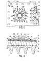
- a support (10) according to the invention is given by way of example.
- the support (10) consists essentially of a substrate (11) formed by an electrically insulating plate, the front face (12) of which is designed to receive at least one integrated circuit device (13) and the rear face (14 ) is intended to cooperate with a cooling device (15), a radiator in the example illustrated.
- the front face (12) of the substrate (11) supports a network (16) of conductors arranged between input-output terminals (17) of the support (10) and studs (18) arranged at the periphery of each zone ( 19) designed to receive an integrated circuit device (13).
- each device (13) has a front face or active face (20) incorporating the elements of the electrical circuits of the device (13) and comprising input-output terminals (21) respectively carrying connecting tabs (22), and a rear face (23).
- the mounting of each device (13) uses a conventional method consisting in placing the rear face (23) of the device (13) on a fixing layer (24) disposed in the center of the zone (19) and in welding the respective ends of the lugs (22) with studs (18) surrounding the area (19).
- the fixing layer (24) advantageously has good thermal conductivity and can be formed by an epoxy layer.
- the contact area of the device (13) with the support (10) therefore has, in this example of attachment of the prior art, the surface of the rear face (23) of the device (13).
- the support (10) comprises at each zone (19) a diffuser element (25) made of a good thermal conductive material, disposed substantially parallel to the front face (12) of the substrate (11) and having a larger area than one of the faces (20, 23) of each device (13).
- the diffusing element is a copper sheet, which is fixed on the network (16) in the zone (19) by a layer (26) and which supports the fixing layer (24) intended to receive a device (13).
- the fixing layer (26) is also advantageously a good thermal conductor, formed for example by a silicone grease.
- the heat dissipated in the face (20) of each device (13) flows in a practically isothermal manner to the rear face (23) of the device (13), passes through the layer of attachment (24), spreads in the diffuser element (25) and then crosses the network (16) and the substrate (11), along a substantially pyramidal channel (27), the small base of which is then formed by the surface of the element (25) and the large base by a part of the rear face (14) of the substrate (11).
- the surface of the diffuser element (25) being significantly higher than that of the faces (20, 23) of the device (13), the heat evacuation channel (27) therefore has in a support (10) conforming to the 'invention a section significantly higher than that of the existing channel in the anterior support.
- the wide channel (27) therefore offers a very reduced thermal resistance to the flow of heat as well as a greater capacity to evacuate high calorific energies.
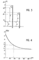
- the advantages of the invention emerge clearly from the graph in FIG. 3 showing the results of experiments with and without the use of a diffusing element (25), all other things being equal.
- the ordinate axis of the graph is representative of temperature differences measured in ° C, while the abscissa axis relates to the temperature at the face (20) of the device (13) and supports two segments (A, B) setting out the results of two experiments made with a device (13) of 2.7mm x 2.7mm side, dissipating 1.3 Watt.
- the segment (A) corresponds to a support of the prior art according to which the device (13) is bonded directly to the network (16) in the area (19), without the intermediary of a diffuser element (25) conforming to the invention; the segment (B) corresponds to the mounting of this device by means of a diffusing element (25) formed by a square copper sheet of 4.5mm side and 0.1mm thick.
- the segments (A) and (B) consist of three sub-segments (a, b, c) which each represent a difference in temperatures taken respectively: for the sub-segment (a) between the active face (20) of the device (13) and the upper face of the network (16) in the area (19), for the sub-segment (b) between the upper face of the network (16) in the area (19) and the front face (12) of the substrate (11), and for the sub-segment (c) between the front face (12) and the rear face (14) of the substrate (11).
- the sub-segments (a) of the segments (A) and (B) are equal and correspond to 8 ° C, while the sub-segment (b) corresponds to 23 ° C for the segment (A) and at 12 ° C only for the segment (B), so that the diffuser element (25) saves in this case 11 ° C for the evacuation of heat only through the network (16).
- the sub-segment (c) corresponds to 4 ° C for the segment (A) and to 3 ° C for the segment (B) between the faces (12) and (14) of the substrate (11).
- the fact that the sub-segment (b) is predominant is due to the high thermal resistance of the electrically insulating material which includes the metallic interconnection network (16).
- the total gain is therefore 12 ° C over 27 ° C (sub-segments b + c of segment A) between the base of the fixing layer (24) of the device (13 ) and the rear face (14) of the substrate (11).
- the diffuser element (25) could be formed in any other way, for example by screen printing at the same time as the formation of the network (16) carried by the face (12a) of the substrate (11). In this case, it could be constituted by any of the layers necessary for the formation of the network (16), or by an additional layer placed on the network (16) in an area (29).
- the advantage of having the diffuser element in the network (16) would reside essentially in the compact arrangement of the studs (18), which could thus be placed immediately alongside each device (13). This arrangement would also allow the attachment of devices (13) without legs (22) by direct connection of the terminals (21) to the studs (18). In this case, the layer (24) would be in contact with the active face (20) of the devices (13).
- FIG. 4 is a graph illustrating a result of experiments carried out to measure the efficiency of a diffuser element (25) formed by a layer of copper deposited by screen printing on the network (16) in an area (29) as a function of the thickness given to this copper layer.
- the experiments were carried out with a device (13) of 6mm x 5mm fixed by a layer (24) to a copper layer (25) of 12mm x 12mm deposited on a network (16) of 245 micrometers.
- the ordinates of the graph in FIG. 4 represent the thermal resistance in ° C / Watt between the diffuser element (25) and the front face (12) of the substrate (11), while the abscissa represents the thickness in micrometers of the diffuser element (25).
Abstract
Description
L'invention a pour objet un support de dispositifs à circuits intégrés.The invention relates to a support for integrated circuit devices.
Les dispositifs à circuits intégrés se présentent sous la forme de plaquettes minces (appelées aussi "puces"), dont la grande face avant, dite face active, incorpore les circuits électroniques et présente les bornes d'entrée-sortie sur lesquelles sont généralement fixées des pattes de raccordement (leads). La face arrière ne comporte aucun circuit. Ces deux faces ont une même surface, dont la valeur varie avec le type du dispositif.Integrated circuit devices are in the form of thin wafers (also called "chips"), the large front face of which, called the active face, incorporates the electronic circuits and presents the input-output terminals to which are generally fixed connection lugs (leads). The rear panel has no circuit. These two faces have the same surface, the value of which varies with the type of device.
Un support de dispositifs à circuits intégrés est formé à partir d'une plaque électriquement isolante, en alumine habituellement, désignée généralement sous le nom de "substrat". La face avant du substrat présente des zones délimitées chacune par des plots destinés à fixer et relier électriquement les pattes ou les bornes d'entrée-sortie d'un dispositif à circuits intégrés. Cette face du substrat comporte aussi un réseau de conducteurs reliant les plots entre eux ainsi qu'à des bornes d'entrée-sortie destinées à la connexion extérieure du support. Ce réseau est formé de plusieurs couches conductrices superposées, espacées par des couches diélectriques.An integrated circuit device carrier is formed from an electrically insulating plate, usually of alumina, generally referred to as a "substrate". The front face of the substrate has zones each delimited by pads intended to fix and electrically connect the tabs or the input-output terminals of an integrated circuit device. This face of the substrate also comprises a network of conductors connecting the pads together as well as to input-output terminals intended for the external connection of the support. This network is made up of several superimposed conductive layers, spaced apart by dielectric layers.
Un problème important lié aux supports de dispositifs de circuits intégrés réside dans l'évacuation des calories engendrées au niveau des faces actives de ces dispositifs. Etant donné les faibles épaisseurs des plaquettes de silicium constituant les puces, on considère que leurs faces avant et arrière sont pratiquement isothermes. Une solution pour évacuer ces calories consiste à monter sur le support un radiateur en contact thermique avec l'une des faces des dispositifs, de sorte que le support n'a qu'un rôle négligeable pour le refroidissement des dispositifs. L'invention concerne l'autre solution, qui consiste au contraire à donner aux supports un rôle important pour la transmission de la chaleur entre les dispositifs et un dispositif de refroidissement connecté à la face arrière du substrat. Tout dispositif de refroidissement bien connu de la technique peut être utilisé, tel qu'un radiateur à ailettes ou à circulation d'eau par exemple.An important problem linked to the supports of integrated circuit devices lies in the evacuation of the calories generated at the active faces of these devices. Given the small thicknesses of the silicon wafers constituting the chips, it is considered that their front and rear faces are practically isothermal. One solution for removing these calories consists in mounting a radiator on the support in thermal contact with one of the faces of the devices, so that the support has only a negligible role in cooling the devices. The invention relates to the other solution, which consists on the contrary in giving the supports an important role for the transmission of heat between the devices and a cooling device connected to the rear face of the substrate. Any cooling device well known in the art can be used, such as a finned or water circulation radiator for example.
Afin de transmettre efficacement les calories produites par les circuits électroniques des dispositifs jusqu'à la face arrière des substrats, les dispositifs ont une de leurs faces formant une plage de contact avec les zones correspondantes de la face avant des substrats. La plage de contact est faite habituellement par une substance de fixation thermocollable, telle qu'une résine époxy. Elles consiste aussi parfois en un soudage par entectique ou en une fusion métal-métal. Dans le cas où les faces actives des dispositifs sont placées en vis-à-vis des zones, la substance de fixation devra être électriquement isolante et bonne conductrice thermique.In order to efficiently transmit the calories produced by the electronic circuits of the devices to the rear face of the substrates, the devices have one of their faces forming a contact area with the corresponding zones of the front face of the substrates. The contact pad is usually made by a heat-bonding fixing substance, such as an epoxy resin. They also sometimes consist of an entectic welding or a metal-metal fusion. In the case where the active faces of the devices are placed facing the zones, the fixing substance must be electrically insulating and good thermal conductor.
Dans les supports, l'expérience montre que la diffusion thermique entre chaque plage de contact et la face arrière du substrat se fait dans un canal sensiblement en forme de tronc de pyramide dont la grande base n'est que légèrement supérieure à la petite base que forme chaque plage de contact. Or, la résistance thermique d'un tel canal étant inversement proportionnelle à la section de celui-ci, ce résultat d'expérience prouve que la résistance thermique est élevée, d'autant plus que le matériau électriquement isolant du substrat et des couches diélectriques du réseau de conducteurs d'interconnexion ne peut avoir qu'un faible coefficient de conductibilité thermique.In the supports, experience shows that the thermal diffusion between each contact pad and the rear face of the substrate takes place in a channel substantially in the shape of a truncated pyramid, the large base of which is only slightly greater than the small base than forms each contact patch. Now, the thermal resistance of such a channel being inversely proportional to the section of the latter, this result of experience proves that the thermal resistance is high, all the more since the electrically insulating material of the substrate and of the dielectric layers of the network of interconnection conductors can only have a low coefficient of thermal conductivity.
Ce problème s'aggrave avec l'emploi actuel de dispositifs à circuits intégrés de haute densité, généralement appelés dispositifs LSI (Large Scale Integration). En effet, la concentration des circuits se traduit par une plus grande dissipation thermique par unité de surface de la face active. Les caractéristiques thermiques du canal d'évacuation de la chaleur étant relativement mauvaises, il est alors très difficile de maintenir la température au niveau de chaque plage à une valeur de seuil souhaitable pour un bon fonctionnement des dispositifs.This problem is aggravated with the current use of high density integrated circuit devices, generally called LSI (Large Scale Integration) devices. In fact, the concentration of the circuits results in greater heat dissipation per unit area of the active face. The thermal characteristics of the heat dissipation channel being relatively poor, it is therefore very difficult to maintain the temperature at each range at a threshold value desirable for proper operation of the devices.
L'invention remédie à tous ces inconvénients.The invention overcomes all these drawbacks.
Selon l'invention, un support présentant une face incluant au moins une zone pour recevoir une face de surface donnée d'un dispositif à circuits intégrés est caractérisé en ce que la zone comporte un élément diffuseur bon conducteur thermique, parallèle à ladite face du support et de surface supérieure à ladite surface donnée.According to the invention, a support having a face including at least one zone for receiving a given surface face of an integrated circuit device is characterized in that the zone comprises a diffuser element that is a good thermal conductor, parallel to said face of the support and of surface greater than said given surface.
En d'autres termes, l'invention consiste à étendre la section du canal de diffusion de la chaleur à travers le support grâce à un élément diffuseur placé au niveau de chaque zone.In other words, the invention consists in extending the section of the heat diffusion channel through the support by means of a diffuser element placed at the level of each zone.
Les caractéristiques et avantages de l'invention ressortiront de la description qui suit, faite en référence aux dessins annexés.The characteristics and advantages of the invention will emerge from the description which follows, given with reference to the accompanying drawings.
Dans les dessins :
- - la figure 1 est une vue fragmentaire de dessus d'un exemple de réalisation d'un support de dispositifs à circuits intégrés conforme à l'invention ;
- - la figure 2 est une vue en coupe suivant la ligne II-II de la figure 1 ;
- - la figure 3 est un graphe illustrant les avantages du support représenté sur les figures 1 et 2 par rapport à un support similaire de la technique antérieure ; et
- - la figure 4 est un autre graphe illustrant les avantages d'une variante de support de dispositifs à circuits intégrés conforme à l'invention par rapport au support tel que représenté sur les figures 1 et 2.
- - Figure 1 is a fragmentary top view of an embodiment of a support for integrated circuit devices according to the invention;
- - Figure 2 is a sectional view along line II-II of Figure 1;
- - Figure 3 is a graph illustrating the advantages of the support shown in Figures 1 and 2 compared to a similar support of the prior art; and
- FIG. 4 is another graph illustrating the advantages of a variant support for integrated circuit devices in accordance with the invention with respect to the support as shown in FIGS. 1 and 2.
En référence aux figures 1 et 2, un support (10) conforme à l'invention est donné à titre d'exemple. Le support (10) est constitué essentiellement d'un substrat (11) formé par une plaque électriquement isolante, dont la face avant (12) est prévue pour recevoir au moins un dispositif à circuits intégrés (13) et dont la face arrière (14) est destinée à coopérer avec un dispositif de refroidissement (15), un radiateur dans l'exemple illustré. La face avant (12) du substrat (11) supporte un réseau (16) de conducteurs disposés entre des bornes d'entrée-sortie (17) du support (10) et des plots (18) disposés à la périphérie de chaque zone (19) prévue pour recevoir un dispositif à circuits intégrés (13). Selon l'exemple illustré, chaque dispositif (13) présente une face avant ou face active (20) incorporant les éléments des circuits électriques du dispositif (13) et comportant des bornes d'entrée-sortie (21) portant respectivement des pattes de liaison (22), et une face arrière (23). Le montage de chaque dispositif (13) utilise un procédé classique consistant à disposer la face arrière (23) du dispositif (13) sur une couche de fixation (24) disposée au centre de la zone (19) et à souder les extrémités respectives des pattes (22) aux plots (18) entourant la zone (19). La couche de fixation (24) a avantageusement une bonne conductibilité thermique et peut être formée par une couche époxy. La plage de contact du dispositif (13) avec le support (10) a donc, dans cet exemple de fixation de la technique antérieure, la surface de la face arrière (23) du dispositif (13).With reference to Figures 1 and 2, a support (10) according to the invention is given by way of example. The support (10) consists essentially of a substrate (11) formed by an electrically insulating plate, the front face (12) of which is designed to receive at least one integrated circuit device (13) and the rear face (14 ) is intended to cooperate with a cooling device (15), a radiator in the example illustrated. The front face (12) of the substrate (11) supports a network (16) of conductors arranged between input-output terminals (17) of the support (10) and studs (18) arranged at the periphery of each zone ( 19) designed to receive an integrated circuit device (13). According to the example illustrated, each device (13) has a front face or active face (20) incorporating the elements of the electrical circuits of the device (13) and comprising input-output terminals (21) respectively carrying connecting tabs (22), and a rear face (23). The mounting of each device (13) uses a conventional method consisting in placing the rear face (23) of the device (13) on a fixing layer (24) disposed in the center of the zone (19) and in welding the respective ends of the lugs (22) with studs (18) surrounding the area (19). The fixing layer (24) advantageously has good thermal conductivity and can be formed by an epoxy layer. The contact area of the device (13) with the support (10) therefore has, in this example of attachment of the prior art, the surface of the rear face (23) of the device (13).
Conformément à l'invention, le suppport (10) comporte au niveau de chaque zone (19) un élément diffuseur (25) en matériau bon conducteur thermique, disposé sensiblement parallèlement à la face avant (12) du substrat (11) et ayant une plus grande surface que l'une des faces (20, 23) de chaque dispositif (13). Dans l'exemple illustré, l'élément diffuseur est une feuille de cuivre, qui est fixée sur le réseau (16) dans la zone (19) par une couche (26) et qui supporte la couche de fixation (24) prévue pour recevoir un dispositif (13). La couche de fixation (26) est aussi avantageusement bonne conductrice thermique, formée par exemple par une graisse de silicone.According to the invention, the support (10) comprises at each zone (19) a diffuser element (25) made of a good thermal conductive material, disposed substantially parallel to the front face (12) of the substrate (11) and having a larger area than one of the faces (20, 23) of each device (13). In the example illustrated, the diffusing element is a copper sheet, which is fixed on the network (16) in the zone (19) by a layer (26) and which supports the fixing layer (24) intended to receive a device (13). The fixing layer (26) is also advantageously a good thermal conductor, formed for example by a silicone grease.
Avec l'élément diffuseur (25), la chaleur dissipée dans la face (20) de chaque dispositif (13) s'écoule de façon pratiquement isotherme jusqu'à la face arrière (23) du dispositif (13), traverse la couche de fixation (24), se répand dans l'élément diffuseur (25) et traverse ensuite le réseau (16) et le substrat (11), suivant un canal (27) sensiblement pyramidal, dont la petite base est alors constituée par la surface de l'élément (25) et la grande base par une partie de la face arrière (14) du substrat (11). La surface de l'élément diffuseur (25) étant notablement plus élevée que celle des faces (20, 23) du dispositif (13), le canal d'évacuation de chaleur (27) a donc dans un support (10) conforme à l'invention une section nettement plus élevée que celle du canal existant dans le support antérieur. Le large canal (27) offre donc une résistance thermique très diminuée à l'écoulement de la chaleur ainsi qu'une plus grand capacité à évacuer de fortes énergies calorifiques. En d'autres termes, il existera par rapport à la technique antérieure une différence de température moins importante entre un dispositif (13) et le dispositif de refroidissement (15), comme cela apparaît à la figure 3.With the diffuser element (25), the heat dissipated in the face (20) of each device (13) flows in a practically isothermal manner to the rear face (23) of the device (13), passes through the layer of attachment (24), spreads in the diffuser element (25) and then crosses the network (16) and the substrate (11), along a substantially pyramidal channel (27), the small base of which is then formed by the surface of the element (25) and the large base by a part of the rear face (14) of the substrate (11). The surface of the diffuser element (25) being significantly higher than that of the faces (20, 23) of the device (13), the heat evacuation channel (27) therefore has in a support (10) conforming to the 'invention a section significantly higher than that of the existing channel in the anterior support. The wide channel (27) therefore offers a very reduced thermal resistance to the flow of heat as well as a greater capacity to evacuate high calorific energies. In other words, compared to the prior art, there will be a smaller temperature difference between a device (13) and the cooling device (15), as shown in FIG. 3.
Les avantages de l'invention ressortent clairement du graphe de la figure 3 exposant des résultats d'expériences avec et sans l'utilisation d'un élément diffuseur (25), toutes choses étant égales par ailleurs. L'axe des ordonnées du graphe est représentatif de différences de températures mesurées en °C, tandis que l'axe des abscisses se rapporte à la température au niveau de la face (20) du dispositif (13) et supporte deux segments (A, B) exposant les résultats de deux expériences faites avec un dispositif (13) de 2,7mm x 2,7mm de côté, dissipant 1,3 Watt. Le segment (A) correspond à un support de la technique antérieure selon laquelle le dispositif (13) est collé directement sur le réseau (16) dans la zone (19), sans l'intermédiaire d'un élément diffuseur (25) conforme à l'invention ; le segment (B) correspond au montage de ce dispositif par l'intermédiaire d'un élément diffuseur (25) formé par une feuille carrée en cuivre de 4,5mm de côté et de 0,1mm d'épaisseur.The advantages of the invention emerge clearly from the graph in FIG. 3 showing the results of experiments with and without the use of a diffusing element (25), all other things being equal. The ordinate axis of the graph is representative of temperature differences measured in ° C, while the abscissa axis relates to the temperature at the face (20) of the device (13) and supports two segments (A, B) setting out the results of two experiments made with a device (13) of 2.7mm x 2.7mm side, dissipating 1.3 Watt. The segment (A) corresponds to a support of the prior art according to which the device (13) is bonded directly to the network (16) in the area (19), without the intermediary of a diffuser element (25) conforming to the invention; the segment (B) corresponds to the mounting of this device by means of a diffusing element (25) formed by a square copper sheet of 4.5mm side and 0.1mm thick.
Les segments (A) et (B) se composent de trois sous-segments (a, b, c) qui représentent chacun une différence de températures prélevées respectivement : pour le sous-segment (a) entre la face active (20) du dispositif (13) et la face supérieure du réseau (16) dans la zone (19), pour le sous-segment (b) entre la face supérieure du réseau (16) dans la zone (19) et la face avant (12) du substrat (11), et pour le sous-segment (c) entre la face avant (12) et la face arrière (14) du substrat (11). Comme cela ressort de la figure 3, les sous-segments (a) des segments (A) et (B) sont égaux et correspondent à 8°C, tandis que le sous-segment (b) correspond à 23°C pour le segment (A) et à 12°C seulement pour le segment (B), si bien que l'élément diffuseur (25) fait gagner dans ce cas 11°C pour l'évacuation de la chaleur seulement à travers le réseau (16). Enfin, le sous-segment (c) correspond à 4°C pour le segment (A) et à 3°C pour le segment (B) entre les faces (12) et (14) du substrat (11). Le fait que le sous-segment (b) soit prédominant est dû à la forte résistance thermique de la matière électriquement isolante qui englobe le réseau métallique d'interconnexion (16). En gagnant encore 1°C à travers le substrat, le gain total est donc de 12°C sur 27°C (sous-segments b+c du segment A) entre la base de la couche de fixation (24) du dispositif (13) et la face arrière (14) du substrat (11).The segments (A) and (B) consist of three sub-segments (a, b, c) which each represent a difference in temperatures taken respectively: for the sub-segment (a) between the active face (20) of the device (13) and the upper face of the network (16) in the area (19), for the sub-segment (b) between the upper face of the network (16) in the area (19) and the front face (12) of the substrate (11), and for the sub-segment (c) between the front face (12) and the rear face (14) of the substrate (11). As shown in Figure 3, the sub-segments (a) of the segments (A) and (B) are equal and correspond to 8 ° C, while the sub-segment (b) corresponds to 23 ° C for the segment (A) and at 12 ° C only for the segment (B), so that the diffuser element (25) saves in this
L'élément diffuseur (25) pourrait être formé d'une tout autre manière, par exemple par sérigraphie en même temps que la formation du réseau (16) porté par la face (12a) du substrat (11). Dans ce cas, il pourrait être constitué par l'une quelconque des couches nécessaires pour la formation du réseau (16), ou par une couche supplémentaire placée sur le réseau (16) dans une zone (29). L'avantage à disposer l'élément diffuseur dans le réseau (16) résiderait essentiellement dans la disposition compacte des plots (18), qui pourraient être ainsi disposés immédiatement aux côtés de chaque dispositif (13). Cette disposition permettrait aussi la fixation de dispositifs (13) sans pattes (22) par connexion directe des bornes (21) aux plots (18). Dans ce cas, la couche (24) serait en contact avec la face active (20) des dispositifs (13).The diffuser element (25) could be formed in any other way, for example by screen printing at the same time as the formation of the network (16) carried by the face (12a) of the substrate (11). In this case, it could be constituted by any of the layers necessary for the formation of the network (16), or by an additional layer placed on the network (16) in an area (29). The advantage of having the diffuser element in the network (16) would reside essentially in the compact arrangement of the studs (18), which could thus be placed immediately alongside each device (13). This arrangement would also allow the attachment of devices (13) without legs (22) by direct connection of the terminals (21) to the studs (18). In this case, the layer (24) would be in contact with the active face (20) of the devices (13).
La figure 4 est un graphe illustrant un résultat d'expériences conduites pour mesurer l'efficacité d'un élément diffuseur (25) formé par une couche de cuivre déposée par sérigraphie sur le réseau (16) dans une zone (29) en fonction de l'épaisseur donnée à cette couche de cuivre. Les expériences ont été faites avec un dispositif (13) de 6mm x 5mm fixé par une couche (24) à une couche de cuivre (25) de 12mm x 12mm déposée sur un réseau (16) de 245 micromètres. Les ordonnées du graphe de la figure 4 représentent la résistance thermique en °C/Watt entre l'élément diffuseur (25) et la face avant (12) du substrat (11), tandis que les abscisses représentent l'épaisseur en micromètres de l'élément diffuseur (25). On voit que l'efficacité varie beaucoup pour de faibles épaisseurs de la couche de diffusion (25), et qu'elle tend ensuite vers une valeur asymptotique R1 de 2,4°C/Watt au-delà de 75 micromètres dans l'exemple illustré. A titre indicatif, on a mesuré dans les mêmes conditions la résistance R2 = 3,5°C/watt avec un élément diffuseur (25) de même surface, formé par une feuille de cuivre de 200 micromètres d'épaisseur et collé sur le réseau comme aux figures 1 et 2, alors que la même résistance R2 est obtenue avec une épaisseur de couche déposée par sérigraphie d'environ 35 micromètres. Une telle différence s'expliquerait d'après les sous-segments (a) de la figure 3, où on voit qu'une couche de fixation telle que (24) ou (26) apporte une résistance thermique notable dans le chemin d'évacuation de la chaleur.FIG. 4 is a graph illustrating a result of experiments carried out to measure the efficiency of a diffuser element (25) formed by a layer of copper deposited by screen printing on the network (16) in an area (29) as a function of the thickness given to this copper layer. The experiments were carried out with a device (13) of 6mm x 5mm fixed by a layer (24) to a copper layer (25) of 12mm x 12mm deposited on a network (16) of 245 micrometers. The ordinates of the graph in FIG. 4 represent the thermal resistance in ° C / Watt between the diffuser element (25) and the front face (12) of the substrate (11), while the abscissa represents the thickness in micrometers of the diffuser element (25). We see that the efficiency varies a lot for small thicknesses of the diffusion layer (25), and that it then tends towards an asymptotic value R 1 of 2.4 ° C / Watt beyond 75 micrometers in the illustrated example. As an indication, the resistance R 2 = 3.5 ° C / watt was measured under the same conditions with a diffuser element (25) of the same surface, formed by a copper sheet 200 micrometers thick and bonded to the network as in FIGS. 1 and 2, while the same resistance R 2 is obtained with a layer thickness deposited by screen printing of approximately 35 micrometers. Such a difference could be explained from the sub-segments (a) of Figure 3, where we see that a fixing layer such as (24) or (26) provides a significant thermal resistance in the evacuation path heat.
Claims (4)
Applications Claiming Priority (2)
| Application Number | Priority Date | Filing Date | Title |
|---|---|---|---|
| FR8207482 | 1982-04-30 | ||
| FR8207482A FR2526226A1 (en) | 1982-04-30 | 1982-04-30 | SUPPORT OF INTEGRATED CIRCUIT DEVICES |
Publications (1)
| Publication Number | Publication Date |
|---|---|
| EP0093659A1 true EP0093659A1 (en) | 1983-11-09 |
Family
ID=9273569
Family Applications (1)
| Application Number | Title | Priority Date | Filing Date |
|---|---|---|---|
| EP83400843A Withdrawn EP0093659A1 (en) | 1982-04-30 | 1983-04-28 | Mounting for integrated circuit devices |
Country Status (3)
| Country | Link |
|---|---|
| EP (1) | EP0093659A1 (en) |
| JP (1) | JPS58204549A (en) |
| FR (1) | FR2526226A1 (en) |
Cited By (1)
| Publication number | Priority date | Publication date | Assignee | Title |
|---|---|---|---|---|
| EP0881679A2 (en) * | 1997-05-27 | 1998-12-02 | Fujitsu Limited | Semiconductor module including a plurality of semiconductor devices detachably |
Citations (1)
| Publication number | Priority date | Publication date | Assignee | Title |
|---|---|---|---|---|
| FR2306530A1 (en) * | 1975-03-31 | 1976-10-29 | Ibm | AIR-COOLED SEMICONDUCTOR PELLET CASE |
-
1982
- 1982-04-30 FR FR8207482A patent/FR2526226A1/en active Pending
-
1983
- 1983-04-28 EP EP83400843A patent/EP0093659A1/en not_active Withdrawn
- 1983-04-30 JP JP58077367A patent/JPS58204549A/en active Pending
Patent Citations (1)
| Publication number | Priority date | Publication date | Assignee | Title |
|---|---|---|---|---|
| FR2306530A1 (en) * | 1975-03-31 | 1976-10-29 | Ibm | AIR-COOLED SEMICONDUCTOR PELLET CASE |
Non-Patent Citations (3)
| Title |
|---|
| IBM TECHNICAL DISCLOSURE BULLETIN, vol. 19, no. 9, février 1977, pages 3321-3322, New York, USA * |
| IBM TECHNICAL DISCLOSURE BULLETIN, vol. 21, no. 4, septembre 1978, pages 1473-1474, New York, USA * |
| IBM TECHNICAL DISCLOSURE BULLETIN, vol. 21, no. 7, décembre 1978, page 2709, New York, USA * |
Cited By (4)
| Publication number | Priority date | Publication date | Assignee | Title |
|---|---|---|---|---|
| EP0881679A2 (en) * | 1997-05-27 | 1998-12-02 | Fujitsu Limited | Semiconductor module including a plurality of semiconductor devices detachably |
| EP0881679A3 (en) * | 1997-05-27 | 2000-08-02 | Fujitsu Limited | Semiconductor module including a plurality of semiconductor devices detachably |
| US6472744B2 (en) | 1997-05-27 | 2002-10-29 | Fujitsu Limited | Semiconductor module including a plurality of semiconductor devices detachably |
| US6696754B2 (en) | 1997-05-27 | 2004-02-24 | Fujitsu Limited | Semiconductor module including a plurality of semiconductor devices detachably |
Also Published As
| Publication number | Publication date |
|---|---|
| JPS58204549A (en) | 1983-11-29 |
| FR2526226A1 (en) | 1983-11-04 |
Similar Documents
| Publication | Publication Date | Title |
|---|---|---|
| EP0308296B1 (en) | Printed circuit comprising a heat sink | |
| CA2074436C (en) | Heat sink | |
| US5712448A (en) | Cooling device featuring thermoelectric and diamond materials for temperature control of heat-dissipating devices | |
| EP1792526B1 (en) | Electronic device provided with an integrated heat spreader | |
| FR2813440A1 (en) | Semiconductor device for electric power control, comprising insulator substrate with front-face circuit pattern and rear-face metallic pattern fastened by soldering on metal base | |
| FR2560731A1 (en) | Thermally conducting multilayer printed card | |
| EP0749160A1 (en) | Method for cooling a housing mounted integrated circuit | |
| EP1005083B1 (en) | High-power electronic device comprising cooling system | |
| FR2937795A1 (en) | Electronic device for use in phototherapy lamp, has support provided with orifice that is arranged opposite to electronic component e.g. LED, where portion of heat conductor element is inserted in orifice | |
| EP1256982A1 (en) | Electronic Module and its Assembling Process | |
| EP0085622B1 (en) | Mounting support for integrated circuit-housing with external leads formed around the housing perimeter | |
| EP1116424B1 (en) | Electronic assembly comprising a sole plate forming a heat sink | |
| FR2511193A1 (en) | Laminated support for cooling semiconductor - has three metal layers including one rigid layer to avoid bi-metallic bending with changing temp. | |
| EP0093659A1 (en) | Mounting for integrated circuit devices | |
| FR2790905A1 (en) | POWER ELECTRICAL COMPONENT MOUNTED BY BRAZING ON A SUPPORT AND ASSEMBLY METHOD THEREFOR | |
| FR2685816A1 (en) | COOLING SYSTEM FOR "MULTI-CHIP" MODULE. | |
| FR2706730A1 (en) | Power electronics module having a heat-sink support | |
| EP0734066B1 (en) | Electronic power module | |
| EP0053967A1 (en) | Removable cooling device for an integrated-circuit mounting | |
| EP0619616B1 (en) | Apparatus exploiting the Peltier effect to detect the risk of condensation on a surface which borders a volume of humid air | |
| FR2571921A1 (en) | HEAT DISSIPATOR FOR ELECTRONIC COMPONENTS WITH CERAMIC SUBSTRATE | |
| EP0080953B1 (en) | Mounting of power components with a branched electrode structure in a pressure contact housing | |
| EP0637826B1 (en) | Power resistor, with device for application under pressure on a heat sink | |
| FR2699039A1 (en) | Multilayer circuit board for use in electronics applications - has circuit board separated by isolating layers with integrated circuits mounted on lower and upper face | |
| FR2787920A1 (en) | METHOD FOR ASSEMBLING A CHIP TO A CIRCUIT MEMBER BY BRAZING |
Legal Events
| Date | Code | Title | Description |
|---|---|---|---|
| PUAI | Public reference made under article 153(3) epc to a published international application that has entered the european phase |
Free format text: ORIGINAL CODE: 0009012 |
|
| AK | Designated contracting states |
Designated state(s): DE FR GB IT SE |
|
| 17P | Request for examination filed |
Effective date: 19831027 |
|
| STAA | Information on the status of an ep patent application or granted ep patent |
Free format text: STATUS: THE APPLICATION IS DEEMED TO BE WITHDRAWN |
|
| 18D | Application deemed to be withdrawn |
Effective date: 19851113 |
|
| RIN1 | Information on inventor provided before grant (corrected) |
Inventor name: BONNEFOY, JEAN |