EP0095211A2 - Magnetron cathode sputtering system - Google Patents
Magnetron cathode sputtering system Download PDFInfo
- Publication number
- EP0095211A2 EP0095211A2 EP83200697A EP83200697A EP0095211A2 EP 0095211 A2 EP0095211 A2 EP 0095211A2 EP 83200697 A EP83200697 A EP 83200697A EP 83200697 A EP83200697 A EP 83200697A EP 0095211 A2 EP0095211 A2 EP 0095211A2
- Authority
- EP
- European Patent Office
- Prior art keywords
- cathode
- rod
- anode
- cathode plate
- sputtering system
- Prior art date
- Legal status (The legal status is an assumption and is not a legal conclusion. Google has not performed a legal analysis and makes no representation as to the accuracy of the status listed.)
- Granted
Links
Images
Classifications
-
- H—ELECTRICITY
- H01—ELECTRIC ELEMENTS
- H01J—ELECTRIC DISCHARGE TUBES OR DISCHARGE LAMPS
- H01J37/00—Discharge tubes with provision for introducing objects or material to be exposed to the discharge, e.g. for the purpose of examination or processing thereof
- H01J37/32—Gas-filled discharge tubes
- H01J37/34—Gas-filled discharge tubes operating with cathodic sputtering
- H01J37/3402—Gas-filled discharge tubes operating with cathodic sputtering using supplementary magnetic fields
- H01J37/3405—Magnetron sputtering
- H01J37/3408—Planar magnetron sputtering
Definitions
- the invention relates to a magnetron cathode sputtering system comprising an envelope, a flat cathode plate consisting at least in a surface layer of material to be sputtered, a substantially ring-shaped anode which is coaxial with the cathode plate, magnetic means disposed on the side of the cathode plate which is remote from the anode and generates at least one closed tunnel of magnetic field lines over a part of the cathode surface, the tunnel forming at least one electron trap.
- Such a magnetron cathode sputtering system is frequently used for providing thin films of a material (for example, a metal) on a substrate.
- a material for example, a metal
- the substrate to be coated is placed in the envelope which is filled with a gas.
- a gas discharge is formed in which gas ions impact on the cathode at high velocity and release material therefrom (mainly atoms).
- This sputtered material is collected by the substrate.
- By providing one or more tunnels of magnetic field lines in front of the cathode which capture electrons emitted by the cathode more ions are formed and hence the sputtering process is intensified.
- the flat cathode may be, for example, square, rectangular or disc-shaped.
- the substantially ring shaped anode is adapted to the shape of the cathode.
- Such a magnetron cathode sputtering system is known from "Vacuum", vol. 28, No. 4, 1978. This article describes a modified magnetron cathode sputtering system. In this system a metal rod extends from the centre of a disc-shaped cathode and forms an elongated pole shoe of a magnetic system. The other pole shoe of said system surrounds and is coaxial with the disc-shaped cathode. The magnetic field between said poleshoes forms the so-called electron trap.
- the diameter of the disc-shaped cathode used in said system was less than 100 mm.
- Such magnetron cathode sputtering systems are used inter alia in the manufacture of semiconductors and for the manufacture of optical record carriers in which a substrate consisting of a thin synthetic plastics or glass disc in which the information is present in the form of a large number of pits is coated with a thin reflecting metal film.
- Such record carriers are used in the video longplay system, VLP system (Trade Mark), of N.V. Philips' Gloeilampenfabrieken described inter alia in Philips Tech. Rev. 33, 178 - 180, 1973, No. 7.
- Such a disc has a diameter of approximately 30 cm and must be covered very uniformly. The disc should not be heated significantly or be exposed to significant electron bombardment, since this may damage the disc. Heating and damage by electrons is not desired either in the manufacture of semiconductors with such a system.
- a magnetron cathode sputtering system of the type mentioned in the opening paragraph is characterized according to the invention in that the electron trap surrounds and is spaced from a rod-shaped electrode extending axially from the centre of the cathode plate, an auxiliary electrode having a tubular cross-section which is coaxial with the cathode plate and extends from near the periphery of the cathode plate, wherein both the rod-shaped electrode and the auxiliary electrode extend from areas on the surface of the cathode plate where no electron trap is present, wherein the bores of the auxiliary electrode and at least of the end portion of the anode which is nearer the cathode plate, the periphery of the cathode plate and the periphery of the rod-shaped electrode are mutually parallel, and wherein during operation of the system the rod-shaped electrode is so spaced from the substrate on which material is to be sputtered that electrons tend to be directed towards the anode.
- the cathode plate can be circular, square or regularly polygonal.
- coaxial cylindrical auxiliary electrodes extending from the cathode surface may also be provided between said electron traps.
- the electric field between the cathode and the anode is thus influenced so that more electrons move towards the anode and do not impinge on the substrate.
- the auxiliary electrodes modify the electric field for the cathode in such a manner that the electrons which are not captured by the electron traps are moved in paths terminating on the anode instead of on the substrate.
- the auxiliary electrodes may have the same potential as the cathode. Because the sputtering of the cathode takes place only from the cathode surface below the electron traps it is not necessary to manufacture the auxiliary electrodes from the material to be sputtered.
- auxiliary electrodes are accommodated so as to be electrically insulated with respect to the cathode, it is possible to vary the potential at the electrodes so that even more electrons are conducted away from the substrate towards the anode.
- VLP system record carriers the central part of the substrate may remain uncovered so that it is possible to provide the rod-shaped auxiliary electrode at its end with a radially extending flange or disc. As a result of this the electric field is modified even more favourably.
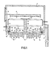
- the magnetron cathode sputtering system shown in Figure 1 comprises an envelope 1, a disc-shaped cathode 2 and a substantially cylindrical anode 3 which is coaxial with the cathode 2.
- the envelope 1 can be evacuated and be filled with a gas (for example with argon) via an exhaust tube 4.
- the envelope 1 furthermore comprises a door 5 to which a holder 6 for a substrate 7 to be sputtered is connected.
- the substrate 7 is a synthetic plastics disc-shaped record carrier for a VLP-system.
- the cathode 2 consists of a 1 cm thick plate of the material to be sputtered, for example aluminium.
- the peripheral ring 8 of a major surface of cathode 2 is connected to an annular flange 10 surrounding an aperture 11 in envelope 1 by means of a gasket 9 of an electrically insulating material.
- a cathode supporting plate 12 abuts the major surface of the cathode 2 which is remote from the anode 3, and a number of magnets 13 are secured to the back of the cathode supporting plate 12 and generate for the surface of cathode 2 closed circumferential tunnels of magnetic field lines 14.
- the electrons originating from the cathode 2 are trapped in said tunnels and then ionize the gas in the envelope 1 close to the cathode surface.
- a coaxial, substantially cylindrical auxiliary electrode 15 is provided between the anode and the cathode 2 near the edge 8 of the cathode 2 and a rod-shaped auxiliary electrode 16 is provided in the centre of the cathode.
- Both the cylindrical auxiliary electrode 15 and the rod-shaped auxiliary electrode 16 are provided near parts 17 and 18 of the cathode where no electron traps are present.
- the distance from the rod-shaped auxiliary electrode to the substrate 7 to be sputtered is chosen so that both the electrons emitted from the parts 17 and 18 and also the electrons emitted from the part 19 of the cathode present between the electron traps are directed as far as possible towards the anode 3.
- auxiliary electrodes between the electron traps (in Figure 1 part 19 of the cathode surface).
- a cylindrical auxiliary electrode 20 is shown in Figure 1 in broken lines.
- the distance from the disc 22 to the substrate 7 is preferably approximately 2 to 3 em.4
- the rod-shaped electrode 16 in this case has a length of approximately 10 cm and a diameter of approximately 3 cm.
- the erosion of a cathode of a magnetron cathode sputtering system is not the same throughout the surface but is concentrated in the centre 23 of the electron trap where a crater is formed after a number of hours in operation.
- the mechanical forces must therefore be received by the cathode supporting plate 12 which hence has to be thick.
- the cathode supporting plate 12 at the area of the magnets 13, however, is chosen to be comparatively thin so as to reduce the magnetic field strength inside the envelope 1 as little as possible. This stronger magnetic field at the cathode surface also results in a better electron yield of the electron traps so that fewer electrons land on the substrate 7.
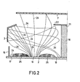
- Figure 2 shows one half of a detail of the sectional view of Figure 1 having therein a number of electrons paths 24 (broken lines) of electrons originating from the parts 17, 18 and 19 of the cathode surface.
- Two circular areas 25 consisting of a quantity of ionized gas are present in front of the cathode 2 and are the result of providing the two electron traps.
- the invention is not restricted to magnetron cathode sputtering systems having circular cathodes and annular anodes but may, of course, also be used in systems having rectangular or square cathodes. Consequently, the circular anodes used in that latter case have a rectangular or square shape. In such systems the cylindrical auxiliary electrodes and rod-shaped auxiliary electrode have a rectangular of square cross-section.
- the distance from the rod-shaped auxiliary electrode 16 to the substrate may also be chosen to be larger than in the embodiment described. However, the operation thereof then becomes less effective.
Abstract
Description
- The invention relates to a magnetron cathode sputtering system comprising an envelope, a flat cathode plate consisting at least in a surface layer of material to be sputtered, a substantially ring-shaped anode which is coaxial with the cathode plate, magnetic means disposed on the side of the cathode plate which is remote from the anode and generates at least one closed tunnel of magnetic field lines over a part of the cathode surface, the tunnel forming at least one electron trap.
- Such a magnetron cathode sputtering system is frequently used for providing thin films of a material (for example, a metal) on a substrate. During operation of the system the substrate to be coated is placed in the envelope which is filled with a gas. By applying a sufficiently high potential between the anode and the cathode, a gas discharge is formed in which gas ions impact on the cathode at high velocity and release material therefrom (mainly atoms). This sputtered material is collected by the substrate. By providing one or more tunnels of magnetic field lines in front of the cathode which capture electrons emitted by the cathode, more ions are formed and hence the sputtering process is intensified. As a result of this the desired coating is more rapidly formed on the substrate. The flat cathode may be, for example, square, rectangular or disc-shaped. The substantially ring shaped anode is adapted to the shape of the cathode. Such a magnetron cathode sputtering system is known from "Vacuum", vol. 28, No. 4, 1978. This article describes a modified magnetron cathode sputtering system. In this system a metal rod extends from the centre of a disc-shaped cathode and forms an elongated pole shoe of a magnetic system. The other pole shoe of said system surrounds and is coaxial with the disc-shaped cathode. The magnetic field between said poleshoes forms the so-called electron trap. The diameter of the disc-shaped cathode used in said system was less than 100 mm.
- Such magnetron cathode sputtering systems are used inter alia in the manufacture of semiconductors and for the manufacture of optical record carriers in which a substrate consisting of a thin synthetic plastics or glass disc in which the information is present in the form of a large number of pits is coated with a thin reflecting metal film. Such record carriers are used in the video longplay system, VLP system (Trade Mark), of N.V. Philips' Gloeilampenfabrieken described inter alia in Philips Tech. Rev. 33, 178 - 180, 1973, No. 7. Such a disc has a diameter of approximately 30 cm and must be covered very uniformly. The disc should not be heated significantly or be exposed to significant electron bombardment, since this may damage the disc. Heating and damage by electrons is not desired either in the manufacture of semiconductors with such a system.
- It is therefore an object of the invention to provide a magnetron cathode sputtering system in which fewer electrons impinge on the substrate to be covered than in the systems used so far as a result of which damage of the substrate is reduced or prevented.
- For that purpose, a magnetron cathode sputtering system of the type mentioned in the opening paragraph is characterized according to the invention in that the electron trap surrounds and is spaced from a rod-shaped electrode extending axially from the centre of the cathode plate, an auxiliary electrode having a tubular cross-section which is coaxial with the cathode plate and extends from near the periphery of the cathode plate, wherein both the rod-shaped electrode and the auxiliary electrode extend from areas on the surface of the cathode plate where no electron trap is present, wherein the bores of the auxiliary electrode and at least of the end portion of the anode which is nearer the cathode plate, the periphery of the cathode plate and the periphery of the rod-shaped electrode are mutually parallel, and wherein during operation of the system the rod-shaped electrode is so spaced from the substrate on which material is to be sputtered that electrons tend to be directed towards the anode.
- The cathode plate can be circular, square or regularly polygonal.
- When two or more electron traps are used, coaxial cylindrical auxiliary electrodes extending from the cathode surface may also be provided between said electron traps. The electric field between the cathode and the anode is thus influenced so that more electrons move towards the anode and do not impinge on the substrate. The auxiliary electrodes modify the electric field for the cathode in such a manner that the electrons which are not captured by the electron traps are moved in paths terminating on the anode instead of on the substrate. During the sputtering process the auxiliary electrodes may have the same potential as the cathode. Because the sputtering of the cathode takes place only from the cathode surface below the electron traps it is not necessary to manufacture the auxiliary electrodes from the material to be sputtered.
- If one or more auxiliary electrodes are accommodated so as to be electrically insulated with respect to the cathode, it is possible to vary the potential at the electrodes so that even more electrons are conducted away from the substrate towards the anode.
- In the above-mentioned VLP system record carriers the central part of the substrate may remain uncovered so that it is possible to provide the rod-shaped auxiliary electrode at its end with a radially extending flange or disc. As a result of this the electric field is modified even more favourably.
- An embodiment of the invention will now be described by way of example, with reference to the drawings, in which
- Figure 1 is a diagrammatic sectional view of a magnetron cathode sputtering system according to the invention and
- Figure 2 shows a number of electron paths in part of such a system.
- The magnetron cathode sputtering system shown in Figure 1 comprises an envelope 1, a disc-
shaped cathode 2 and a substantiallycylindrical anode 3 which is coaxial with thecathode 2. The envelope 1 can be evacuated and be filled with a gas (for example with argon) via an exhaust tube 4. The envelope 1 furthermore comprises adoor 5 to which aholder 6 for a substrate 7 to be sputtered is connected. In this case the substrate 7 is a synthetic plastics disc-shaped record carrier for a VLP-system. Thecathode 2 consists of a 1 cm thick plate of the material to be sputtered, for example aluminium. Theperipheral ring 8 of a major surface ofcathode 2 is connected to anannular flange 10 surrounding an aperture 11 in envelope 1 by means of a gasket 9 of an electrically insulating material. Acathode supporting plate 12 abuts the major surface of thecathode 2 which is remote from theanode 3, and a number ofmagnets 13 are secured to the back of thecathode supporting plate 12 and generate for the surface ofcathode 2 closed circumferential tunnels ofmagnetic field lines 14. The electrons originating from thecathode 2 are trapped in said tunnels and then ionize the gas in the envelope 1 close to the cathode surface. By trapping a part of the electrons emitted by thecathode 2 in the electron traps, more ions are formed than without the use of said electron traps and the sputtering process is intensified. Because a part of the electrons emitted by the cathode are not captured and partly impinge on the substrate 7, measures have to be taken to prevent heating and damage of said substrate 7. Therefore according to the invention, a coaxial, substantially cylindricalauxiliary electrode 15 is provided between the anode and thecathode 2 near theedge 8 of thecathode 2 and a rod-shapedauxiliary electrode 16 is provided in the centre of the cathode. Both the cylindricalauxiliary electrode 15 and the rod-shapedauxiliary electrode 16 are provided nearparts parts part 19 of the cathode present between the electron traps are directed as far as possible towards theanode 3. - When more than one electron trap is used it is possible to provide cylindrical auxiliary electrodes between the electron traps (in Figure 1
part 19 of the cathode surface). As an example, a cylindricalauxiliary electrode 20 is shown in Figure 1 in broken lines. - It is possible to arrange one or more of the cylindrical
auxiliary electrodes auxiliary electrode 16 in an electrically insulated manner with respect to thecathode 2 and to vary the potential at said electrodes so that even more electrons are directed towards theanode 3 instead of towards the substrate 7. By providing the rod-shapedauxiliary electrode 16 at itsend 21 with a radially extendingdisc 22, the electric field can be modified even more favourably. - With a diameter of the substrate 7 of approximately 30 cm, the distance from the
disc 22 to the substrate 7 is preferably approximately 2 to 3 em.4 The rod-shaped electrode 16 in this case has a length of approximately 10 cm and a diameter of approximately 3 cm. - The erosion of a cathode of a magnetron cathode sputtering system is not the same throughout the surface but is concentrated in the
centre 23 of the electron trap where a crater is formed after a number of hours in operation. The mechanical forces must therefore be received by thecathode supporting plate 12 which hence has to be thick. Thecathode supporting plate 12 at the area of themagnets 13, however, is chosen to be comparatively thin so as to reduce the magnetic field strength inside the envelope 1 as little as possible. This stronger magnetic field at the cathode surface also results in a better electron yield of the electron traps so that fewer electrons land on the substrate 7. - Figure 2 shows one half of a detail of the sectional view of Figure 1 having therein a number of electrons paths 24 (broken lines) of electrons originating from the
parts cathode 2 and are the result of providing the two electron traps. By providing the cylindricalauxiliary electrode 15 and the rod-shapedauxiliary electrode 16, the number of electrons incident on the substrate 7 can be drastically reduced as a result of which the substrate 7 is not damaged due to heating and electron bombardment. The cylindricalauxiliary electrodes auxiliary electrode 16 are present near therespective parts - The invention is not restricted to magnetron cathode sputtering systems having circular cathodes and annular anodes but may, of course, also be used in systems having rectangular or square cathodes. Consequently, the circular anodes used in that latter case have a rectangular or square shape. In such systems the cylindrical auxiliary electrodes and rod-shaped auxiliary electrode have a rectangular of square cross-section. The distance from the rod-shaped
auxiliary electrode 16 to the substrate may also be chosen to be larger than in the embodiment described. However, the operation thereof then becomes less effective.
Claims (6)
Priority Applications (1)
| Application Number | Priority Date | Filing Date | Title |
|---|---|---|---|
| AT83200697T ATE29623T1 (en) | 1982-05-21 | 1983-05-17 | MAGNETRON CATHODATION SYSTEM. |
Applications Claiming Priority (2)
| Application Number | Priority Date | Filing Date | Title |
|---|---|---|---|
| NL8202092A NL8202092A (en) | 1982-05-21 | 1982-05-21 | MICROWAVE CATHODES SPUTTER SYSTEM. |
| NL8202092 | 1982-05-21 |
Publications (3)
| Publication Number | Publication Date |
|---|---|
| EP0095211A2 true EP0095211A2 (en) | 1983-11-30 |
| EP0095211A3 EP0095211A3 (en) | 1984-05-09 |
| EP0095211B1 EP0095211B1 (en) | 1987-09-09 |
Family
ID=19839767
Family Applications (1)
| Application Number | Title | Priority Date | Filing Date |
|---|---|---|---|
| EP83200697A Expired EP0095211B1 (en) | 1982-05-21 | 1983-05-17 | Magnetron cathode sputtering system |
Country Status (8)
| Country | Link |
|---|---|
| US (1) | US4427524A (en) |
| EP (1) | EP0095211B1 (en) |
| JP (1) | JPS58210167A (en) |
| AT (1) | ATE29623T1 (en) |
| AU (1) | AU557135B2 (en) |
| CA (1) | CA1193998A (en) |
| DE (1) | DE3373590D1 (en) |
| NL (1) | NL8202092A (en) |
Cited By (10)
| Publication number | Priority date | Publication date | Assignee | Title |
|---|---|---|---|---|
| GB2143255A (en) * | 1983-07-06 | 1985-02-06 | Leybold Heraeus Gmbh & Co Kg | Magnetron cathode for cathodic evaporation installations |
| EP0162643A1 (en) * | 1984-05-17 | 1985-11-27 | Varian Associates, Inc. | Sputter coating source having plural target rings |
| US4606806A (en) * | 1984-05-17 | 1986-08-19 | Varian Associates, Inc. | Magnetron sputter device having planar and curved targets |
| EP0316523A2 (en) * | 1987-11-16 | 1989-05-24 | Leybold Aktiengesellschaft | Control for sputtering according to the magnetron principle |
| DE4202211A1 (en) * | 1992-01-28 | 1993-07-29 | Leybold Ag | Sputter installation - has at least one magnetron cathode and an electrically insulated screen limiting plasma propagation |
| NL1000139C2 (en) * | 1995-04-13 | 1996-10-15 | Od & Me Bv | Microwave sputtering system. |
| US5863399A (en) * | 1996-04-13 | 1999-01-26 | Singulus Technologies Gmbh | Device for cathode sputtering |
| US5997697A (en) * | 1995-10-06 | 1999-12-07 | Balzers Aktiengesellschaft | Magnetron sputtering source and method of use thereof |
| DE19947932C1 (en) * | 1999-09-28 | 2001-04-26 | Fraunhofer Ges Forschung | Device for magnetron sputtering has an outer plasma electrode with a first potential arranged between a target and a counter electrode with a second potential |
| ES2374775A1 (en) * | 2009-04-03 | 2012-02-22 | Universidad De Castilla La Mancha | Cathodic spray unit of circular white. (Machine-translation by Google Translate, not legally binding) |
Families Citing this family (23)
| Publication number | Priority date | Publication date | Assignee | Title |
|---|---|---|---|---|
| US4508612A (en) * | 1984-03-07 | 1985-04-02 | International Business Machines Corporation | Shield for improved magnetron sputter deposition into surface recesses |
| JPS62287073A (en) * | 1986-06-04 | 1987-12-12 | Sony Corp | Cathode device for magnetron sputtering |
| US4728406A (en) * | 1986-08-18 | 1988-03-01 | Energy Conversion Devices, Inc. | Method for plasma - coating a semiconductor body |
| US4738761A (en) * | 1986-10-06 | 1988-04-19 | Microelectronics Center Of North Carolina | Shared current loop, multiple field apparatus and process for plasma processing |
| DE3634710A1 (en) * | 1986-10-11 | 1988-04-21 | Ver Glaswerke Gmbh | DEVICE FOR VACUUM COATING A GLASS DISC BY REACTIVE CATHODAL SPRAYING |
| DE3721373A1 (en) * | 1987-06-29 | 1989-01-12 | Leybold Ag | COATING DEVICE |
| KR970002340B1 (en) * | 1988-07-15 | 1997-03-03 | 미쓰비시 가세이 가부시끼가이샤 | Method for producing magnetic recording medium |
| JP2934711B2 (en) * | 1989-12-07 | 1999-08-16 | カシオ計算機株式会社 | Sputtering equipment |
| US5298720A (en) * | 1990-04-25 | 1994-03-29 | International Business Machines Corporation | Method and apparatus for contamination control in processing apparatus containing voltage driven electrode |
| US5045166A (en) * | 1990-05-21 | 1991-09-03 | Mcnc | Magnetron method and apparatus for producing high density ionic gas discharge |
| US5080772A (en) * | 1990-08-24 | 1992-01-14 | Materials Research Corporation | Method of improving ion flux distribution uniformity on a substrate |
| DE4221930C2 (en) * | 1991-11-21 | 2001-04-05 | Leybold Ag | Device for the adhesive coating of a plastic substrate |
| JP2570594Y2 (en) * | 1991-12-17 | 1998-05-06 | 日新電機株式会社 | Thin film forming equipment |
| DE19614599A1 (en) * | 1996-04-13 | 1997-10-16 | Singulus Technologies Gmbh | Apparatus for cathode sputtering in substrate coating installations |
| DE19614595A1 (en) * | 1996-04-13 | 1997-10-16 | Singulus Technologies Gmbh | Apparatus for cathode sputtering in substrate coating |
| US6783638B2 (en) * | 2001-09-07 | 2004-08-31 | Sputtered Films, Inc. | Flat magnetron |
| JP4563629B2 (en) * | 2001-11-19 | 2010-10-13 | 株式会社エフ・ティ・エスコーポレーション | Opposite target type sputtering system |
| US8038850B2 (en) * | 2006-06-23 | 2011-10-18 | Qimonda Ag | Sputter deposition method for forming integrated circuit |
| US20080083611A1 (en) * | 2006-10-06 | 2008-04-10 | Tegal Corporation | High-adhesive backside metallization |
| US8808513B2 (en) * | 2008-03-25 | 2014-08-19 | Oem Group, Inc | Stress adjustment in reactive sputtering |
| US20090246385A1 (en) * | 2008-03-25 | 2009-10-01 | Tegal Corporation | Control of crystal orientation and stress in sputter deposited thin films |
| US8482375B2 (en) * | 2009-05-24 | 2013-07-09 | Oem Group, Inc. | Sputter deposition of cermet resistor films with low temperature coefficient of resistance |
| US9127356B2 (en) * | 2011-08-18 | 2015-09-08 | Taiwan Semiconductor Manufacturing Co., Ltd. | Sputtering target with reverse erosion profile surface and sputtering system and method using the same |
Citations (5)
| Publication number | Priority date | Publication date | Assignee | Title |
|---|---|---|---|---|
| GB1111910A (en) * | 1964-12-31 | 1968-05-01 | Ibm | Improvements in or relating to cathode sputtering |
| US3897325A (en) * | 1972-10-20 | 1975-07-29 | Nippon Electric Varian Ltd | Low temperature sputtering device |
| US4198283A (en) * | 1978-11-06 | 1980-04-15 | Materials Research Corporation | Magnetron sputtering target and cathode assembly |
| JPS5585672A (en) * | 1978-12-25 | 1980-06-27 | Nec Corp | Sputtering apparatus |
| DE3004546A1 (en) * | 1979-02-19 | 1980-08-21 | Hiradastech Ipari Kutato | PENNING SPRAYING SOURCE |
-
1982
- 1982-05-21 NL NL8202092A patent/NL8202092A/en not_active Application Discontinuation
-
1983
- 1983-05-06 US US06/492,107 patent/US4427524A/en not_active Expired - Fee Related
- 1983-05-17 EP EP83200697A patent/EP0095211B1/en not_active Expired
- 1983-05-17 AT AT83200697T patent/ATE29623T1/en not_active IP Right Cessation
- 1983-05-17 DE DE8383200697T patent/DE3373590D1/en not_active Expired
- 1983-05-19 CA CA000428547A patent/CA1193998A/en not_active Expired
- 1983-05-19 AU AU14682/83A patent/AU557135B2/en not_active Ceased
- 1983-05-20 JP JP58087822A patent/JPS58210167A/en active Granted
Patent Citations (5)
| Publication number | Priority date | Publication date | Assignee | Title |
|---|---|---|---|---|
| GB1111910A (en) * | 1964-12-31 | 1968-05-01 | Ibm | Improvements in or relating to cathode sputtering |
| US3897325A (en) * | 1972-10-20 | 1975-07-29 | Nippon Electric Varian Ltd | Low temperature sputtering device |
| US4198283A (en) * | 1978-11-06 | 1980-04-15 | Materials Research Corporation | Magnetron sputtering target and cathode assembly |
| JPS5585672A (en) * | 1978-12-25 | 1980-06-27 | Nec Corp | Sputtering apparatus |
| DE3004546A1 (en) * | 1979-02-19 | 1980-08-21 | Hiradastech Ipari Kutato | PENNING SPRAYING SOURCE |
Non-Patent Citations (1)
| Title |
|---|
| PATENTS ABSTRACTS OF JAPAN, vol. 4, no. 135 (C-25)[617], 20th September 1980, page 95 C 25 & JP - A - 55 085 672 (NIPPON DENKI K.K.) 27-06-1980 * |
Cited By (17)
| Publication number | Priority date | Publication date | Assignee | Title |
|---|---|---|---|---|
| GB2143255A (en) * | 1983-07-06 | 1985-02-06 | Leybold Heraeus Gmbh & Co Kg | Magnetron cathode for cathodic evaporation installations |
| EP0162643A1 (en) * | 1984-05-17 | 1985-11-27 | Varian Associates, Inc. | Sputter coating source having plural target rings |
| US4606806A (en) * | 1984-05-17 | 1986-08-19 | Varian Associates, Inc. | Magnetron sputter device having planar and curved targets |
| EP0316523A2 (en) * | 1987-11-16 | 1989-05-24 | Leybold Aktiengesellschaft | Control for sputtering according to the magnetron principle |
| EP0316523A3 (en) * | 1987-11-16 | 1991-01-16 | Leybold Aktiengesellschaft | Control for sputtering according to the magnetron principle |
| DE4202211A1 (en) * | 1992-01-28 | 1993-07-29 | Leybold Ag | Sputter installation - has at least one magnetron cathode and an electrically insulated screen limiting plasma propagation |
| NL1000139C2 (en) * | 1995-04-13 | 1996-10-15 | Od & Me Bv | Microwave sputtering system. |
| EP0737999A1 (en) * | 1995-04-13 | 1996-10-16 | ODME International B.V. | A magnetron sputtering system |
| US5868914A (en) * | 1995-04-13 | 1999-02-09 | Odme International B.V. | Magnetron sputtering system |
| CH691643A5 (en) * | 1995-10-06 | 2001-08-31 | Unaxis Balzers Ag | Magnetron sputtering and the use thereof. |
| US5997697A (en) * | 1995-10-06 | 1999-12-07 | Balzers Aktiengesellschaft | Magnetron sputtering source and method of use thereof |
| DE19639240C2 (en) * | 1995-10-06 | 2000-03-02 | Balzers Hochvakuum | Magnetron sputtering source and its use |
| US6540883B1 (en) | 1995-10-06 | 2003-04-01 | Unaxis Balzers Aktiengesellschaft | Magnetron sputtering source and method of use thereof |
| NL1004217C2 (en) * | 1995-10-06 | 2001-07-19 | Balzers Hochvakuum | Microwave atomizing source and its use. |
| US5863399A (en) * | 1996-04-13 | 1999-01-26 | Singulus Technologies Gmbh | Device for cathode sputtering |
| DE19947932C1 (en) * | 1999-09-28 | 2001-04-26 | Fraunhofer Ges Forschung | Device for magnetron sputtering has an outer plasma electrode with a first potential arranged between a target and a counter electrode with a second potential |
| ES2374775A1 (en) * | 2009-04-03 | 2012-02-22 | Universidad De Castilla La Mancha | Cathodic spray unit of circular white. (Machine-translation by Google Translate, not legally binding) |
Also Published As
| Publication number | Publication date |
|---|---|
| EP0095211A3 (en) | 1984-05-09 |
| JPH0227433B2 (en) | 1990-06-18 |
| AU1468283A (en) | 1983-11-24 |
| DE3373590D1 (en) | 1987-10-15 |
| NL8202092A (en) | 1983-12-16 |
| AU557135B2 (en) | 1986-12-04 |
| JPS58210167A (en) | 1983-12-07 |
| US4427524A (en) | 1984-01-24 |
| ATE29623T1 (en) | 1987-09-15 |
| EP0095211B1 (en) | 1987-09-09 |
| CA1193998A (en) | 1985-09-24 |
Similar Documents
| Publication | Publication Date | Title |
|---|---|---|
| US4427524A (en) | Magnetron cathode sputtering system | |
| EP1489643B1 (en) | Method and apparatus for ionized physical vapor deposition | |
| US4581118A (en) | Shaped field magnetron electrode | |
| US6117279A (en) | Method and apparatus for increasing the metal ion fraction in ionized physical vapor deposition | |
| US4038171A (en) | Supported plasma sputtering apparatus for high deposition rate over large area | |
| US4434042A (en) | Planar magnetron sputtering apparatus | |
| EP0088463B1 (en) | Magnetron cathode sputtering system | |
| JPH05171423A (en) | Deflection electron gun device for vacuum deposition | |
| EP0737999B1 (en) | A magnetron sputtering system | |
| US3875028A (en) | Method of manufacture of x-ray tube having focusing cup with non emitting coating | |
| US4927515A (en) | Circular magnetron sputtering device | |
| CA1204700A (en) | Magnetron reactive bias sputtering method and apparatus | |
| US5378341A (en) | Conical magnetron sputter source | |
| US2752519A (en) | Method and apparatus for use in chemical evaporation processes | |
| US5711860A (en) | Method and apparatus for producing a substrate with low secondary electron emissions | |
| JPH023262B2 (en) | ||
| US2919380A (en) | Electron discharge devices | |
| GB1600904A (en) | Image intensifier tubes | |
| JP2849771B2 (en) | Sputter type ion source | |
| JP2001164360A (en) | Dc sputtering system | |
| US4370586A (en) | Image intensifier tube having an internal alkali baffle | |
| US20070158178A1 (en) | Method and apparatus for deposition of low-k dielectric materials | |
| JPS62216225A (en) | Manufacturing apparatus of semiconductor | |
| Spindt et al. | Development program on a cold cathode electron gun | |
| JPS63266065A (en) | Film forming device |
Legal Events
| Date | Code | Title | Description |
|---|---|---|---|
| PUAI | Public reference made under article 153(3) epc to a published international application that has entered the european phase |
Free format text: ORIGINAL CODE: 0009012 |
|
| AK | Designated contracting states |
Designated state(s): AT DE FR GB SE |
|
| PUAL | Search report despatched |
Free format text: ORIGINAL CODE: 0009013 |
|
| AK | Designated contracting states |
Designated state(s): AT DE FR GB SE |
|
| 17P | Request for examination filed |
Effective date: 19840720 |
|
| 17Q | First examination report despatched |
Effective date: 19860220 |
|
| D17Q | First examination report despatched (deleted) | ||
| GRAA | (expected) grant |
Free format text: ORIGINAL CODE: 0009210 |
|
| AK | Designated contracting states |
Kind code of ref document: B1 Designated state(s): AT DE FR GB SE |
|
| REF | Corresponds to: |
Ref document number: 29623 Country of ref document: AT Date of ref document: 19870915 Kind code of ref document: T |
|
| REF | Corresponds to: |
Ref document number: 3373590 Country of ref document: DE Date of ref document: 19871015 |
|
| ET | Fr: translation filed | ||
| PLBE | No opposition filed within time limit |
Free format text: ORIGINAL CODE: 0009261 |
|
| STAA | Information on the status of an ep patent application or granted ep patent |
Free format text: STATUS: NO OPPOSITION FILED WITHIN TIME LIMIT |
|
| 26N | No opposition filed | ||
| PGFP | Annual fee paid to national office [announced via postgrant information from national office to epo] |
Ref country code: GB Payment date: 19930430 Year of fee payment: 11 |
|
| PGFP | Annual fee paid to national office [announced via postgrant information from national office to epo] |
Ref country code: AT Payment date: 19930524 Year of fee payment: 11 |
|
| PGFP | Annual fee paid to national office [announced via postgrant information from national office to epo] |
Ref country code: SE Payment date: 19930526 Year of fee payment: 11 Ref country code: FR Payment date: 19930526 Year of fee payment: 11 |
|
| PGFP | Annual fee paid to national office [announced via postgrant information from national office to epo] |
Ref country code: DE Payment date: 19930729 Year of fee payment: 11 |
|
| PG25 | Lapsed in a contracting state [announced via postgrant information from national office to epo] |
Ref country code: GB Effective date: 19940517 Ref country code: AT Effective date: 19940517 |
|
| PG25 | Lapsed in a contracting state [announced via postgrant information from national office to epo] |
Ref country code: SE Effective date: 19940518 |
|
| GBPC | Gb: european patent ceased through non-payment of renewal fee |
Effective date: 19940517 |
|
| EUG | Se: european patent has lapsed |
Ref document number: 83200697.7 Effective date: 19941210 |
|
| PG25 | Lapsed in a contracting state [announced via postgrant information from national office to epo] |
Ref country code: FR Effective date: 19950131 |
|
| PG25 | Lapsed in a contracting state [announced via postgrant information from national office to epo] |
Ref country code: DE Effective date: 19950201 |
|
| EUG | Se: european patent has lapsed |
Ref document number: 83200697.7 |
|
| REG | Reference to a national code |
Ref country code: FR Ref legal event code: ST |