EP0095283A2 - Memory device - Google Patents
Memory device Download PDFInfo
- Publication number
- EP0095283A2 EP0095283A2 EP83302665A EP83302665A EP0095283A2 EP 0095283 A2 EP0095283 A2 EP 0095283A2 EP 83302665 A EP83302665 A EP 83302665A EP 83302665 A EP83302665 A EP 83302665A EP 0095283 A2 EP0095283 A2 EP 0095283A2
- Authority
- EP
- European Patent Office
- Prior art keywords
- memory device
- semi
- layers
- layer
- amorphous
- Prior art date
- Legal status (The legal status is an assumption and is not a legal conclusion. Google has not performed a legal analysis and makes no representation as to the accuracy of the status listed.)
- Withdrawn
Links
- 239000004065 semiconductor Substances 0.000 claims abstract description 18
- 239000000758 substrate Substances 0.000 claims abstract description 17
- 230000001143 conditioned effect Effects 0.000 claims abstract description 6
- 239000011521 glass Substances 0.000 claims abstract description 6
- 229910052710 silicon Inorganic materials 0.000 claims abstract description 6
- 239000010703 silicon Substances 0.000 claims abstract description 6
- AMGQUBHHOARCQH-UHFFFAOYSA-N indium;oxotin Chemical compound [In].[Sn]=O AMGQUBHHOARCQH-UHFFFAOYSA-N 0.000 claims abstract description 4
- UFHFLCQGNIYNRP-UHFFFAOYSA-N Hydrogen Chemical compound [H][H] UFHFLCQGNIYNRP-UHFFFAOYSA-N 0.000 claims description 11
- 239000001257 hydrogen Substances 0.000 claims description 11
- 229910052739 hydrogen Inorganic materials 0.000 claims description 11
- 239000002243 precursor Substances 0.000 claims description 10
- 238000000034 method Methods 0.000 claims description 9
- 239000000463 material Substances 0.000 claims description 7
- BLRPTPMANUNPDV-UHFFFAOYSA-N Silane Chemical group [SiH4] BLRPTPMANUNPDV-UHFFFAOYSA-N 0.000 claims description 6
- 229910000077 silane Inorganic materials 0.000 claims description 6
- 238000002485 combustion reaction Methods 0.000 claims description 2
- 238000002360 preparation method Methods 0.000 claims description 2
- 230000002269 spontaneous effect Effects 0.000 claims description 2
- XOLBLPGZBRYERU-UHFFFAOYSA-N tin dioxide Chemical compound O=[Sn]=O XOLBLPGZBRYERU-UHFFFAOYSA-N 0.000 claims description 2
- 229910001887 tin oxide Inorganic materials 0.000 claims description 2
- 239000004020 conductor Substances 0.000 abstract description 2
- XYFCBTPGUUZFHI-UHFFFAOYSA-N Phosphine Chemical compound P XYFCBTPGUUZFHI-UHFFFAOYSA-N 0.000 description 6
- XUIMIQQOPSSXEZ-UHFFFAOYSA-N Silicon Chemical compound [Si] XUIMIQQOPSSXEZ-UHFFFAOYSA-N 0.000 description 4
- 229910021417 amorphous silicon Inorganic materials 0.000 description 4
- 239000004411 aluminium Substances 0.000 description 3
- 229910052782 aluminium Inorganic materials 0.000 description 3
- XAGFODPZIPBFFR-UHFFFAOYSA-N aluminium Chemical compound [Al] XAGFODPZIPBFFR-UHFFFAOYSA-N 0.000 description 3
- 238000006243 chemical reaction Methods 0.000 description 3
- 229910000073 phosphorus hydride Inorganic materials 0.000 description 3
- RZVAJINKPMORJF-UHFFFAOYSA-N Acetaminophen Chemical compound CC(=O)NC1=CC=C(O)C=C1 RZVAJINKPMORJF-UHFFFAOYSA-N 0.000 description 2
- 230000000694 effects Effects 0.000 description 2
- 239000005297 pyrex Substances 0.000 description 2
- ZOXJGFHDIHLPTG-UHFFFAOYSA-N Boron Chemical compound [B] ZOXJGFHDIHLPTG-UHFFFAOYSA-N 0.000 description 1
- 229910052796 boron Inorganic materials 0.000 description 1
- 230000003750 conditioning effect Effects 0.000 description 1
- 230000008021 deposition Effects 0.000 description 1
- 239000007789 gas Substances 0.000 description 1
- BHEPBYXIRTUNPN-UHFFFAOYSA-N hydridophosphorus(.) (triplet) Chemical compound [PH] BHEPBYXIRTUNPN-UHFFFAOYSA-N 0.000 description 1
- 238000004519 manufacturing process Methods 0.000 description 1
- 229910052751 metal Inorganic materials 0.000 description 1
- 239000002184 metal Substances 0.000 description 1
- 239000013080 microcrystalline material Substances 0.000 description 1
- 239000000203 mixture Substances 0.000 description 1
- 239000000700 radioactive tracer Substances 0.000 description 1
- 229910001220 stainless steel Inorganic materials 0.000 description 1
- 239000010935 stainless steel Substances 0.000 description 1
- 239000011043 treated quartz Substances 0.000 description 1
Images

Classifications
-
- H—ELECTRICITY
- H01—ELECTRIC ELEMENTS
- H01L—SEMICONDUCTOR DEVICES NOT COVERED BY CLASS H10
- H01L23/00—Details of semiconductor or other solid state devices
- H01L23/52—Arrangements for conducting electric current within the device in operation from one component to another, i.e. interconnections, e.g. wires, lead frames
- H01L23/522—Arrangements for conducting electric current within the device in operation from one component to another, i.e. interconnections, e.g. wires, lead frames including external interconnections consisting of a multilayer structure of conductive and insulating layers inseparably formed on the semiconductor body
- H01L23/525—Arrangements for conducting electric current within the device in operation from one component to another, i.e. interconnections, e.g. wires, lead frames including external interconnections consisting of a multilayer structure of conductive and insulating layers inseparably formed on the semiconductor body with adaptable interconnections
- H01L23/5252—Arrangements for conducting electric current within the device in operation from one component to another, i.e. interconnections, e.g. wires, lead frames including external interconnections consisting of a multilayer structure of conductive and insulating layers inseparably formed on the semiconductor body with adaptable interconnections comprising anti-fuses, i.e. connections having their state changed from non-conductive to conductive
-
- G—PHYSICS
- G11—INFORMATION STORAGE
- G11C—STATIC STORES
- G11C17/00—Read-only memories programmable only once; Semi-permanent stores, e.g. manually-replaceable information cards
- G11C17/14—Read-only memories programmable only once; Semi-permanent stores, e.g. manually-replaceable information cards in which contents are determined by selectively establishing, breaking or modifying connecting links by permanently altering the state of coupling elements, e.g. PROM
- G11C17/16—Read-only memories programmable only once; Semi-permanent stores, e.g. manually-replaceable information cards in which contents are determined by selectively establishing, breaking or modifying connecting links by permanently altering the state of coupling elements, e.g. PROM using electrically-fusible links
-
- H—ELECTRICITY
- H01—ELECTRIC ELEMENTS
- H01L—SEMICONDUCTOR DEVICES NOT COVERED BY CLASS H10
- H01L29/00—Semiconductor devices adapted for rectifying, amplifying, oscillating or switching, or capacitors or resistors with at least one potential-jump barrier or surface barrier, e.g. PN junction depletion layer or carrier concentration layer; Details of semiconductor bodies or of electrodes thereof ; Multistep manufacturing processes therefor
- H01L29/66—Types of semiconductor device ; Multistep manufacturing processes therefor
- H01L29/86—Types of semiconductor device ; Multistep manufacturing processes therefor controllable only by variation of the electric current supplied, or only the electric potential applied, to one or more of the electrodes carrying the current to be rectified, amplified, oscillated or switched
- H01L29/861—Diodes
- H01L29/8615—Hi-lo semiconductor devices, e.g. memory devices
-
- H—ELECTRICITY
- H01—ELECTRIC ELEMENTS
- H01L—SEMICONDUCTOR DEVICES NOT COVERED BY CLASS H10
- H01L2924/00—Indexing scheme for arrangements or methods for connecting or disconnecting semiconductor or solid-state bodies as covered by H01L24/00
- H01L2924/0001—Technical content checked by a classifier
- H01L2924/0002—Not covered by any one of groups H01L24/00, H01L24/00 and H01L2224/00
Abstract
Description
- This invention relates to a memory device of novel structure incorporating amorphous or microcrystalline semiconducting material and to a process for the production of amorphous silicon suitable for use in such a device.
- A memory device based on amorphous silicon has previously been disclosed. IEE Proc. Vol 129, Pt 1,
No 2, April 1982, pages 51-54 discloses a structure consisting in its simplest form of p and n layers deposited onto a conducting stainless steel substrate. The layered structure is conditioned into a memory device by applying a large forward bias which enables the structure to be put into a stable state (either "on" or "off") by applying a voltage pulse of known polarity. The device can then be switched to an alternative "on" or "off" state by applying a voltage pulse above a certain threshold such as 4V with opposite polarity to the original pulse. - We have now discovered that memory devices having a different configuration of silicon layers in which no two p and n layers are adjacent have this property (which is herein referred to as a memory), that similar devices can also be made on substrates permeable to light and that such memory devices can be influenced by light.
- Thus according to the present invention there is provided a memory device comprising an electrically conducting substrate and layers of i and p and/or n type amorphous or microcrystalline semi- conducting material which have been conditioned by the application of a voltage sufficiently large to cause the structure to be permanently modified to reduce the electrical resistance of the layers wherein no p and n layers are adjacent in the device.
- We believe that the operation of the device according to the present invention is governed by the properties of the i layer thereby giving enhanced control of the device.
- It is to be understood that p type and n type include p and p+ and n and n+ within their respective scopes.
- Preferably, layers of p type and i type amorphous or microcrystalline semi-conducting material are deposited on to the substrate to form a p-i configuration.
- Most preferably an additional layer of n type amorphous or microcrystalline semi-conducting material is deposited to form a p-i-n configuration.
- The amorphous or microcrystalline semi-conducting material is preferably silicon.
- The substrate can be a modified glass, the surface of which has been rendered electrically conducting by a layer of tin oxide, indium tin oxide or other light permeable electrical conducting material. An advantage of using an optically transparent substrate is that light may be used to affect the stable states of the device.
- The substrate may also be a similarly treated quartz.
- oesirably the device includes one or more electrically conducting areas on the outer surface of the silicon layer remote from the substrate. These areas can conveniently be provided by strips or spots of a metal such as aluminium.
- The layer of i type material can be prepared by methods known in the art, for example by decomposing a gaseous hydrogen-containing precursor of the material, e.g., silane, in a glow discharge. The layers of p type and n type material can be prepared by adding diborane or phosphine respectively in varying quantities to the precursor.
- According to another aspect of the present invention there is provided a method for the preparation of an amorphous semi-conducting material suitable for use in a memory device which method comprises the step of decomposing a gaseous hydrogen-containing precursor of the semi-conducting material in the presence of hydrogen wherein the concentration of the precursor in hydrogen is below that at which spontaneous combustion occurs and the pressure is controlled to form amorphous material.
- A suitable precursor is silane.
- The concentration of the precursor in hydrogen is preferably not greater than 5% by volume.
- The total pressure is preferably in the range 1 to 5 torr.
- The conditioning voltage is preferably in the
range 5 to 20 volts greater than the threshold switching voltage. Once conditioned, the device can be put into either of two stable states, "on" or "off", by applying a voltage above a certain threshold, usually approximately 4 volts, and reversed by applying a voltage of the opposite polarity to its predecessor. - The device is non-volatile, that is to say, once the device has been put into one of the stable states, it remains there even if the power to the device is removed.
- The invention is illustrated by the following Examples.
- An ITO (indium tin oxide) coated glass substrate was placed on a temperature variable substrate holder, the whole being inside a cylindrical Pyrex reaction chamber. The chamber was evacuated to 10-2 torr with a trapped rotary pump and the substrate heated to 300°C. A mixture of 4X by volume silane in hydrogen was admitted to the chamber to bring the pressure up to about 3 torr. Once the pressure had stabilised 2X by vol of diborane was added to the silane in the chamber. A glow discharge was initiated by exciting external coils encircling the pyrex vessel from a LFE radio frequency generator operating at 13.56 M Hz. This caused p type amorphous silicon containing boron to be deposited on the ITO coated glass from the gas phase. After one minute the diborane flow was terminated, thus causing a region of intrinsic (or undoped) material to be produced on top of the p type region. This situation was maintained for 30 minutes. Finally, 0.1% by vol phosphine was progressively admitted to the reaction chamber and growth continued for a further six minutes. This caused n type amorphous silicon containing phosphorous to be deposited on top of the i type material. At this stage the discharge was extinguished, the phosphine flow was stopped and the device was allowed to cool under a flow of 4X silane in hydrogen. When the device had cooled to room temperature it was removed from the reaction chamber and placed in a vacuum coater, where several spots of
aluminium 2 mm in diameter were evaporated onto the surface of the device. - The complete structure is shown in Fig. 1 wherein 1 represents the glass substrate, 2 the layer of ITO, 3 the layer of p type silicon, 4 the layer of i type, 5 the layer of n type and 6 the aluminium spots. The p layer is about 200Å thick, the n layer about 500A and the i layer about 4300Å.
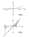
- The device was placed on a curve tracer and its voltage/current characteristics examined. Usually they were of the form as shown in Fig 2. Finally a large voltage (10-20V) was applied to the device. This step 'conditions' the device into a memory (switching) device with the characteristics as shown in Fig 3.
- Curves A and B in Fig 3 show the device in its OFF state. Applying negative bias (curve A) has no effect on the conductivity state, applying forward bias (curve B) causes the device to switch to an intermediate conductivity state (curve C) at about 2V. Further forward bias finally switches the device to its ON state, (curve D). Higher forward potentials have no further effect on the conductivity state. Applying negative bias now leaves the device in the 0N state (curve E) until a potential of 5V is attained, whereupon it immediately switches to its OFF state (curve A). This sequence of events is repeatable with no change in the ON-OFF conductivity or switching levels.
- A similar device was constructed from microcrystalline material. This was prepared in a similar manner to that disclosed in Example 1 with the difference that the deposition pressure was reduced to 0.8 torr. It was then conditioned as before.
Claims (10)
Applications Claiming Priority (2)
| Application Number | Priority Date | Filing Date | Title |
|---|---|---|---|
| GB8214204 | 1982-05-15 | ||
| GB8214204 | 1982-05-15 |
Publications (2)
| Publication Number | Publication Date |
|---|---|
| EP0095283A2 true EP0095283A2 (en) | 1983-11-30 |
| EP0095283A3 EP0095283A3 (en) | 1984-12-27 |
Family
ID=10530383
Family Applications (1)
| Application Number | Title | Priority Date | Filing Date |
|---|---|---|---|
| EP83302665A Withdrawn EP0095283A3 (en) | 1982-05-15 | 1983-05-11 | Memory device |
Country Status (3)
| Country | Link |
|---|---|
| US (1) | US4567499A (en) |
| EP (1) | EP0095283A3 (en) |
| JP (1) | JPS58210661A (en) |
Cited By (4)
| Publication number | Priority date | Publication date | Assignee | Title |
|---|---|---|---|---|
| WO1985002709A1 (en) * | 1983-12-10 | 1985-06-20 | The British Petroleum Company P.L.C. | Memory device |
| GB2153147A (en) * | 1984-01-13 | 1985-08-14 | British Petroleum Co Plc | Threshold switch |
| EP0162529A1 (en) * | 1984-01-13 | 1985-11-27 | The British Petroleum Company p.l.c. | Amorphous or microcrystalline semiconductor memory device |
| US5360981A (en) * | 1989-05-11 | 1994-11-01 | British Telecommunications Public Limited Company | Amorphous silicon memory |
Families Citing this family (2)
| Publication number | Priority date | Publication date | Assignee | Title |
|---|---|---|---|---|
| JPS6188578A (en) * | 1984-10-08 | 1986-05-06 | Nec Corp | Non-linear element |
| FR2581781B1 (en) * | 1985-05-07 | 1987-06-12 | Thomson Csf | NON-LINEAR CONTROL ELEMENTS FOR FLAT ELECTROOPTIC DISPLAY SCREEN AND MANUFACTURING METHOD THEREOF |
Citations (2)
| Publication number | Priority date | Publication date | Assignee | Title |
|---|---|---|---|---|
| DE3036869A1 (en) * | 1979-10-01 | 1981-04-16 | Hitachi, Ltd., Tokyo | INTEGRATED SEMICONDUCTOR CIRCUIT, CIRCUIT PROGRAMMING SYSTEM AND CIRCUIT PROGRAMMING METHOD |
| DE3000905A1 (en) * | 1978-03-16 | 1981-07-16 | Energy Conversion Devices Inc., 48084 Troy, Mich. | Amorpher halbleiter |
Family Cites Families (19)
| Publication number | Priority date | Publication date | Assignee | Title |
|---|---|---|---|---|
| US3571670A (en) * | 1968-04-11 | 1971-03-23 | Energy Conversion Devices Inc | tching device including boron and silicon, carbon or the like |
| US3571672A (en) * | 1968-04-11 | 1971-03-23 | Energy Conversion Devices Inc | Switching device including silicon and carbon |
| US3571673A (en) * | 1968-08-22 | 1971-03-23 | Energy Conversion Devices Inc | Current controlling device |
| US3796931A (en) * | 1969-09-27 | 1974-03-12 | Licentia Gmbh | P-n junction semiconductor device provided with an insulating layer having two stable resistance states |
| US3740620A (en) * | 1971-06-22 | 1973-06-19 | Ibm | Storage system having heterojunction-homojunction devices |
| US3758797A (en) * | 1971-07-07 | 1973-09-11 | Signetics Corp | Solid state bistable switching device and method |
| US3886577A (en) * | 1973-09-12 | 1975-05-27 | Energy Conversion Devices Inc | Filament-type memory semiconductor device and method of making the same |
| US4064521A (en) * | 1975-07-28 | 1977-12-20 | Rca Corporation | Semiconductor device having a body of amorphous silicon |
| US4177474A (en) * | 1977-05-18 | 1979-12-04 | Energy Conversion Devices, Inc. | High temperature amorphous semiconductor member and method of making the same |
| US4177475A (en) * | 1977-10-31 | 1979-12-04 | Burroughs Corporation | High temperature amorphous memory device for an electrically alterable read-only memory |
| US4203123A (en) * | 1977-12-12 | 1980-05-13 | Burroughs Corporation | Thin film memory device employing amorphous semiconductor materials |
| US4485389A (en) * | 1978-03-08 | 1984-11-27 | Energy Conversion Devices, Inc. | Amorphous semiconductors equivalent to crystalline semiconductors |
| US4226643A (en) * | 1979-07-16 | 1980-10-07 | Rca Corporation | Method of enhancing the electronic properties of an undoped and/or N-type hydrogenated amorphous silicon film |
| US4371883A (en) * | 1980-03-14 | 1983-02-01 | The Johns Hopkins University | Current controlled bistable electrical organic thin film switching device |
| JPS56147488A (en) * | 1980-04-18 | 1981-11-16 | Sanyo Electric Co Ltd | Solar cell |
| JPS56165371A (en) * | 1980-05-26 | 1981-12-18 | Shunpei Yamazaki | Semiconductor device |
| JPS5778185A (en) * | 1980-11-01 | 1982-05-15 | Semiconductor Energy Lab Co Ltd | Semiconductor photoelectric converter |
| US4453173A (en) * | 1982-04-27 | 1984-06-05 | Rca Corporation | Photocell utilizing a wide-bandgap semiconductor material |
| JPS59108370A (en) * | 1982-12-14 | 1984-06-22 | Kanegafuchi Chem Ind Co Ltd | Photovoltaic device |
-
1983
- 1983-05-11 EP EP83302665A patent/EP0095283A3/en not_active Withdrawn
- 1983-05-12 US US06/494,009 patent/US4567499A/en not_active Expired - Fee Related
- 1983-05-14 JP JP58084884A patent/JPS58210661A/en active Pending
Patent Citations (2)
| Publication number | Priority date | Publication date | Assignee | Title |
|---|---|---|---|---|
| DE3000905A1 (en) * | 1978-03-16 | 1981-07-16 | Energy Conversion Devices Inc., 48084 Troy, Mich. | Amorpher halbleiter |
| DE3036869A1 (en) * | 1979-10-01 | 1981-04-16 | Hitachi, Ltd., Tokyo | INTEGRATED SEMICONDUCTOR CIRCUIT, CIRCUIT PROGRAMMING SYSTEM AND CIRCUIT PROGRAMMING METHOD |
Non-Patent Citations (2)
| Title |
|---|
| JAPAN JOURNAL OF APPLIED PHYSICS, vol. 13, no. 5, 1974; TOKYO (JP) Y. AKIBA et al.: "Asymmetric Switching and Memory Characteristics in Amorphous Semiconductor", pages 915-916. * |
| JOURNAL OF APPLIED PHYSICS, vol. 46, no. 5, May 1975, American Institute of Physics; NEW YORK (US) S. PURKISS et al.: "Switching and polarity-dependent memory effects in Se-SnO2 and Se-In2O3 thin-film devices", pages 2301-2303. * |
Cited By (6)
| Publication number | Priority date | Publication date | Assignee | Title |
|---|---|---|---|---|
| WO1985002709A1 (en) * | 1983-12-10 | 1985-06-20 | The British Petroleum Company P.L.C. | Memory device |
| EP0152689A2 (en) * | 1983-12-10 | 1985-08-28 | The British Petroleum Company p.l.c. | Memory device |
| EP0152689A3 (en) * | 1983-12-10 | 1985-09-25 | The British Petroleum Company p.l.c. | Memory device |
| GB2153147A (en) * | 1984-01-13 | 1985-08-14 | British Petroleum Co Plc | Threshold switch |
| EP0162529A1 (en) * | 1984-01-13 | 1985-11-27 | The British Petroleum Company p.l.c. | Amorphous or microcrystalline semiconductor memory device |
| US5360981A (en) * | 1989-05-11 | 1994-11-01 | British Telecommunications Public Limited Company | Amorphous silicon memory |
Also Published As
| Publication number | Publication date |
|---|---|
| JPS58210661A (en) | 1983-12-07 |
| EP0095283A3 (en) | 1984-12-27 |
| US4567499A (en) | 1986-01-28 |
Similar Documents
| Publication | Publication Date | Title |
|---|---|---|
| EP0162529B1 (en) | Amorphous or microcrystalline semiconductor memory device | |
| US5238866A (en) | Plasma enhanced chemical vapor deposition process for producing an amorphous semiconductive surface coating | |
| US4490229A (en) | Deposition of diamondlike carbon films | |
| Meyerson et al. | Chemical modification of the electrical properties of hydrogenated amorphous carbon films | |
| EP0032788A1 (en) | Method for depositing coatings in a glow discharge | |
| JPS58197775A (en) | Thin film transistor | |
| US3849276A (en) | Process for forming reactive layers whose thickness is independent of time | |
| US4492736A (en) | Process for forming microcrystalline silicon material and product | |
| US4446168A (en) | Method of forming amorphous silicon | |
| EP0095283A2 (en) | Memory device | |
| US4339470A (en) | Fabricating amorphous silicon solar cells by varying the temperature _of the substrate during deposition of the amorphous silicon layer | |
| EP0115124B1 (en) | Memory device incorporating an amorphous or microcrystalline alloy | |
| Ando et al. | Bias effects on the deposition of hydrogenated amorphous silicon film in a glow discharge | |
| KR20000069692A (en) | Semiconducting devices and method of making thereof | |
| US4266984A (en) | Enhanced open circuit voltage in amorphous silicon photovoltaic devices | |
| US4711807A (en) | Insulating material of non-single crystalline silicon compound | |
| JP2000273617A (en) | Production of transparent electrically conductive film | |
| JPH08264486A (en) | Semiconductor electrode forming method and apparatus | |
| Tardy et al. | Glow discharge mass spectrometry of silicon DC sputtering in argon-hydrogen | |
| US4508932A (en) | Silicon-based solar energy conversion cells | |
| US4551352A (en) | Method of making P-type hydrogenated amorphous silicon | |
| JP2547204B2 (en) | Method for forming bismuth titanate thin film | |
| JP2994056B2 (en) | Thin-film two-terminal element | |
| JPS5943575A (en) | Semiconductor element | |
| JPS5980932A (en) | Plasma treating device |
Legal Events
| Date | Code | Title | Description |
|---|---|---|---|
| PUAI | Public reference made under article 153(3) epc to a published international application that has entered the european phase |
Free format text: ORIGINAL CODE: 0009012 |
|
| AK | Designated contracting states |
Designated state(s): BE DE FR GB IT NL |
|
| PUAL | Search report despatched |
Free format text: ORIGINAL CODE: 0009013 |
|
| AK | Designated contracting states |
Designated state(s): BE DE FR GB IT NL |
|
| 17P | Request for examination filed |
Effective date: 19850530 |
|
| 17Q | First examination report despatched |
Effective date: 19860422 |
|
| D17Q | First examination report despatched (deleted) | ||
| STAA | Information on the status of an ep patent application or granted ep patent |
Free format text: STATUS: THE APPLICATION IS DEEMED TO BE WITHDRAWN |
|
| 18D | Application deemed to be withdrawn |
Effective date: 19901127 |
|
| RIN1 | Information on inventor provided before grant (corrected) |
Inventor name: THWAITES, MICHAEL JOHN Inventor name: HOCKLEY, PETER JOHNDEPARTMENT OF PHYSICS |