EP0095721A2 - Semiconductor memory device - Google Patents
Semiconductor memory device Download PDFInfo
- Publication number
- EP0095721A2 EP0095721A2 EP83105182A EP83105182A EP0095721A2 EP 0095721 A2 EP0095721 A2 EP 0095721A2 EP 83105182 A EP83105182 A EP 83105182A EP 83105182 A EP83105182 A EP 83105182A EP 0095721 A2 EP0095721 A2 EP 0095721A2
- Authority
- EP
- European Patent Office
- Prior art keywords
- memory
- power source
- auxiliary
- mos transistor
- circuit
- Prior art date
- Legal status (The legal status is an assumption and is not a legal conclusion. Google has not performed a legal analysis and makes no representation as to the accuracy of the status listed.)
- Granted
Links
Images


Classifications
-
- G—PHYSICS
- G11—INFORMATION STORAGE
- G11C—STATIC STORES
- G11C29/00—Checking stores for correct operation ; Subsequent repair; Testing stores during standby or offline operation
- G11C29/70—Masking faults in memories by using spares or by reconfiguring
- G11C29/78—Masking faults in memories by using spares or by reconfiguring using programmable devices
- G11C29/83—Masking faults in memories by using spares or by reconfiguring using programmable devices with reduced power consumption
- G11C29/832—Masking faults in memories by using spares or by reconfiguring using programmable devices with reduced power consumption with disconnection of faulty elements
Definitions
- the present invention relates to a semiconductor memory device with an improved yield.
- auxiliary memory in addition to a main memory, so that, when the main memory contains an error bit, the auxiliary memory is used in place of the error bit, thus saving the defective main memory.
- this example provides a redundancy function for the main memory containing the error bit by the p rovi- sion of the auxiliary memory.
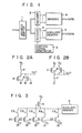
- FIG. 1 A schematic illustration of the semiconductor memory device with such an auxiliary memory is given in Fig. 1.
- an output signal from an address buffer 1 is applied to a main address decoder 2 and an auxiliary address decoder 3.
- a decoded output of the main address decoder 2 is applied to a main memory 4, thereby selecting one of the row lines in the main memory.
- data is written into or read out from the memory cells coupled with the row lines selected, by a write signal or a read signal.
- the main address decoder 2 is controlled in its decode operation by the output from the auxiliary address decoder 3.
- the decoded output of the auxiliary memory 5 to select one of the row lines in the auxiliary address decoder 3 is applied to the auxiliary memory 5 to select one of the row lines in the auxiliary memory 5. Then, data is written into the memory cell connectd to the selected row line using write signal and read out of the same by a read signal.
- the auxiliary address decoder 3 is so programmed that when the main memory 4 contains an error bit cell, it produces the decoded output corresponding to the address of the error bit cell. Therefore, when an error bit cell in the main memory 4 is selected, the output of the auxiliary decoder 3 selects the auxiliary memory 5.
- an error bit cell is selected means "a row line connected to an error bit cell is selected", for ease of explanation.
- an auxiliary memory 5 is selected is used to mean "a row line connected to the memory cell of the auxiliary memory 5, which is used in place of the error bit cell in the main memory, is selected”.
- the auxiliary address decoder 3 operates under the control of an error bit replacement control signal generator 6 for generating a control signal for error bit replacement.
- the error bit replacement control signal generator 6 which includes nonvolatile memory elements, stores the information which, when an error bit is contained in the main memory 4, operates the auxiliary decoder so as to select the bit cell of the auxiliary memory 5 in place of the error bit cell.
- the control signal generator 6 outputs a control signal for the error bit replacement to the auxiliary address decoder 3 on the basis of the information, thereby controlling the operation.
- a correct bit cell is selected means "a row line connected to a correct bit cell is selected”.
- the auxiliary address decoder 3 selects a memory cell in the auxiliary memory 5. Further, at this time, the decoded output of the auxiliary address decoder 3 stops the decoding operation of the main address decoder 2, blocking access to the main memory 4. Through this operation, the error bit cell in the main memory 4 is replaced with a memory cell in the auxiliary memory 5.
- Figs. 2A and 2B show circuit diagrams of two examples of the error bit replacement control signal generator 6.
- a fuse element F made of polysilicon as a nonvolatile memory element is inserted between a power source VD and an output terminal Out.
- a programming enhancement-type MOS tran - sistor 7 is inserted between the output terminal Out and ground.
- a depletion-type MOS transistor 8 is inserted between the output terminal Out and ground.
- a programming signal P is applied to the gate of the MOS transistor 7.
- the MOS transistor 8 is connected to ground.
- a programming enhancement-type MOS transistor 7 is inserted between a power source VD applying point and an output terminal Out.
- a depletion-type MOS transistor 8 is inserted between the VD applying point and the output terminal Out.
- a fuse F is connected between the output terminal Out and ground.
- a programming signal P is applied to the gate of the MOS transistor 7 and the gate of the MOS transistor 8 is coupled to the output terminal Out.
- Fig. 3 shows a configuration of the auxiliary address decoder 3 when no error bit replacement control signal generator 6 is used.
- the auxiliary address decoder is comprised of a depletion-type MOS transistor 9, a plurality of drive MOS transistors 10 of the enhancement type, having at their inputs address signals A0, A0, Al, A1, ... An produced from the address buffer 1, and a plurality of fuses FB inserted between the MOS transistors 10 and 9.
- This programming is performed by burning out the fuse FB connected to the MOS transistor 10 receiving the address signals AO, A1, ... An at the gate.
- Fig. 4 shows another embodiment of a prior auxiliary memory.
- This auxiliary decoder does not use the fuse elements FB used in the auxiliary decoder of Fig. 3 but uses programming circuits instead.
- the programming circuits are respectively provided for the drive transistors 10 in a one-to-one corresponding manner. For ease of illustration, only one programming circuit denoted as "lli" is illustrated.
- the drive transistor 10i is gate-controlled by a programming circuit Ci derived from the programming circuit lli.
- the other drive transistors 10 0 to 10 m are gate-controlled by programming signals applied from the corresponding programming circuits.
- an enhancement-type MOS transistor 10 DR is provided in parallel with the drive transistors 10 0 to 10 m .
- the programming circuit 10i is comprised of a fuse element FC, enhancement-type MOS transistors 12 to 17, and depletion-type MOS transistors 18 to 20.
- the drain-source paths of the MOS transistors 12 and 13 are coupled at one end with an address signals Ai and Ai, respectively.
- a control signal for error bit replacement generated and delivered from the control signal generator 6 (see Fig . . 1) is input to the gates of the transistors 16 and 17.
- An output signal OUT derived from the error bit replacement control signal generator 6 is also applied to the gate of the parallel-connected transistor 10 DR .
- the other ends of the MOS transistors 12 and 13 are connected together and the common connection point provides an output terminal connected to the gate of the drive transistor 10i.
- the replacement signal OUT is set at logical "I".
- the MOS transistor 10 DR is turned on, and therefore the auxiliary memory is not selected.
- the replacement signal OUT is logical "0".
- the programming circuit lli produces the input address signal Ai as the output signal Ci.
- the programming signal Ci from the programming circuit lli is logical "0" and the drive transistor 10i supplied with the programming signal Ci is off. Therefore, when all other drive transistors 10 0 to 10 m are off, the auxiliary memory is selected.
- the circuit lli produces an input address signal Ai as a programming signal Ci.
- CMOSRAM's complementary MOS transistors
- This extremely small current may be, for example, a leak current flowing through the transistor, a leak current due to detection of an PN junction, a short current in the memory bit cell when the power source and ground are shorted by an extremely large resistor element in the memory cell, or the like. These currents are extremely small, and do not lead to the destruction of data in the memory bit cell. Therefore, the conventional detecting method judges the memory bit cell with such an extremely small current as a correct memory cell. In other words, the conventional detecting method cannot detect memory cells with an extremely small current.
- an object of the present invention is to provide a semiconductor memory device which can prevent wasteful power dissipation due to current flow in a decoder circuit or a memory area not being used.
- Another object of the present invention is to provide a semiconductor memory device which can detect a memory bit cell in which an extremely small current, such as a leak current, flows.
- a semiconductor memory device comprising:
- a semiconductor memory device comprising:
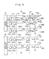
- Fig. 5 shows an embodiment of a semiconductor memory device according to the present invention.
- a main memory 21 is comprised of memory cells 22 11 to 22 1m and 22 21 to 22 2m provided at intersections of a plurality of row lines R Ml to R Mn and a plurality of column lines Cl to Cm.
- the outputs of a main row decoder 23 are connected to the row lines R M1 to RMn of the main memory 21.
- the main row decoder 23 decodes an input row address signal to select one of the row lines RMl to R Mn .
- the selection of the row line drives the memory cells connected to the selected row line.
- a column decoder is provided to decode an input column address signal to select one of the column lines Cl to Cm. Data is read out from a memory cell at the intersection of the selected row line and the selected column line.
- Power source lines 24 Ml to 24 Mn are provided for row lines R M1 to R Mn , respectively.
- the power source lines 24 Ml to 24 Mn are respectively connected to memory cells 22 1l to 22 1m and 22 21 to 22 2m connected to the corresponding row lines R Ml to R Mn , as shown.
- the power source line 24 Ml is connected to the memory cells 22 11 to 22 1m connected to the corresponding row line R Al .
- the power source lines 24 Ml to 24 Mn are connected through fuse elements FD Ml to FD Mn to a power source VD.
- the power source lines 24 Ml to 24 Mn are provided with fusing circuits CM 1 to CM n for fusing the fuse elements, respectively. These fusing circuits all have the same construction, and so only the fusing circuit CM l will be described.
- the fusing circuit CM l is comprised of two depletion-type MOS transistors 25 1 and 25 2 connected in series between the row line R Ml and a high voltage power source VP, and two enhancement-type MOS transistors 26 1 and 26 2 connected in series between the power source line 24 Ml and the reference voltage (e.g., ground) VS.
- the transistor 25 1 is connected at the source to the row line R Ml and at the drain to the source of a transistor 25 2 .
- the drain of the transistor 25 2 is connected to the high power source VD.
- a signal P of logical "0" is applied to the gate of the transistor 25 1 when the fuse element FD Ml is burned out.
- the gate of the transistor 25 2 is connected to the source thereof.
- the transistor 26 1 is connected at the drain to the power source line 24 Ml and at the source to the drain of the transistor 26 2 .
- the source of the transistor 26 2 is connected to the reference voltage VS. When the fuse element FD M1 is burned out, a signal of logical "1" is applied to the gate of the transistor 26 1 .
- the gate of the transistor 26 2 is connected to the gate and the source of the transistor 25 2 .
- An auxiliary memory 27 is provided for saving the main memory with an error bit. This auxiliary memory 27 is not used when the error bit cell is not contained in the main memory 21.
- the auxiliary memory 27 is comprised of memory cells 28 11 to 28 1m and 28 21 to 28 2m provided at the intersections of row lines R Al to R An and column lines Cl to Cn.
- an error bit cell is, for example, the memory cell 22 1l of the memory cells 22 1l to 22 1m connected to the row line R Ml , for example, in the main memory 21, the correct data to be written into the memory cells 22 11 to 22 1m on the row line R Ml is written into the memory cells 28 1l to 28 1m on the row line R Al .
- the outputs of an auxiliary decoder 29 are connected to the row lines R Al to R An of the auxiliary memory 27.
- the auxiliary decoder 29 receives an input address signal which is input to the main row decoder 23.
- the auxiliary decoder 29 is so programmed that when an address signal to select the row line containing the error bit cell of the main memory 21 is received, it selects a corresponding row line with a memory cell storing the correct data in the auxiliary memory
- main memory 21 and auxiliary memory 27 are separately illustrated. They may be fabricated such that they are arranged in different memory areas within a single memory device. This can be applied to the arrangement of the decoders 23 and 29.
- power source lines 24 Al to 24An are correspondingly provided for the row lines R A1 to R An , as in the main memory 21.
- the power source lines 24 Al to 24An are connected to memory cells 28 1l to 28 1m and 28 21 to 28 2m which are connected to the corresponding row lines R Al to R An .
- the power source line 24 Al is connected to the memory cells 28 1l to 28 1m connected to the row lines R Al corresponding to the power source line 24 Al .
- the power source lines 24 Al to 24An are connected to the power source VD through fuse elements FD Al to FD An made of polysilicon, for example, as in the main memory 21.
- Fusing circuits CA1 to CAn for fusing the fuse elements FD Al to FD An are connected to power source lines 24 Al to 24An, respectively.
- the fusing circuit CAl is constructed of an enhancement-type MOS transistor 30 whose drain is connected to the power source line 24 AI and the source to the reference voltage VS. A signal of logical "1" is applied to the gate of a transistor 30 when the fuse element FD Al is burned.
- the same is true of the fusing circuit CA1, and so no further explanations will be provided in this regard.
- the power source voltage VD is applied through the power source lines 24 Ml to 24 M2 and the main memory 21 is kept in an operation mode.
- the power source voltage VD is applied to the memory cells 28 1l to 28 1m and 28 21 to 28 2m of the auxiliary memory 27, through the power source lines 24 Al to 24An, and the auxiliary memory 27 is kept in an operation mode.
- the auxiliary memory 27 When no error bit cell is contained in the main memory 21, the auxiliary memory 27 is not used. In this case, the power source supply VD to the auxiliary memory 27 is shut off to place the auxiliary memory 27 in an inoperative mode. This results in a saving of power.
- the output of the power source VD to the auxiliary memory 27 is shut off by applying a signal PR of logical "1" to the gates of the transistors 30 1 to 30 2 of the fusing circuits CA1 to CAn. When the logical "1" signal is applied to the gates of these transistors, the transistors 30 1 to 30 2 are turned on, so that heavy current flows into the fuse elements FD Al to FD An connected between the transistors 30 1 and 30 2 and the power source voltage VD.
- the row line R Ml is not selected. Accordingly, in this case, power is saved by shutting off the supply of power to the memory cells 22 11 to 22 1m connected to the row line R A1 .
- an address input signal for selecting the row line R M1 is input to the main row decoder 23 to select the row line R M1 . Then, the row line R M1 is logical "1". Then, the signal P is set at logical "0" and the signal P at logical "1".
- the transistor 25 1 connected to the row line R M1 is turned off, so that the high power source voltage VP is applied to the gate of the transistor 26 2 via the drain-source path of the transistor 25 2 .
- the transistors 26 1 and 26 2 are conductive and a large current flows into the fuse element FD M1 . Joule heat generated by the flow of this large current burns out the fuse element FD M1 .
- the power source line 24 Ml corresponding to the row line R M1 is separated from the power source VD. As a result, the power supply to the memory cells 22 1l to 22 1m is shut off to save power used for this memory device.
- the row line R Ml When the row line R Ml is selected, the'remaining row lines R M2 to R Mn are in a non-selected state. In this case, the transistors associated with the row lines R M2 to R Mn , which correspond to the non-selected row lines R M2 to R Mn are logical "0". Therefore, the fuse elements FD M2 to FD Mn of the power source lines 24 M1 to 24 M2 corresponding to the row lines R M1 to R Mn are not fused. As a result, the memory cells 22 11 to 22 1m and 22 21 to 22 2m coupled with the power source lines 24 M2 to 24 Mn are kept in an operation mode.
- the power source VD may be used in place of the high power source voltage VP.
- the fuse elements FD M1 to FD Mn were burned-out by feeding the current to the fuse elements, a laser beam may be used for burning out the fuse elements. If the laser beam is used, there is no need for the transistors 25 1 , 25 2 , 26 1 and 26 2 and the transistors 30 1 , 30 2 ....
- the power line is separated or disconnected from the power source VD by burning the fuse element.
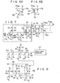
- the separation or disconnection of the power line from the power source VD is not limited to the above method. Another example for executing such power source separation will be described referring to Figs. 6A and 6B.
- the circuit shown in Figs. 6A and 6B is so designed that an enhancement-type MOS transistor 31 is provided between the power source VD and the power source line 24 M1 .
- the power source separation is performed by turning off the MOS transistor 31.
- the transistor 31 is provided between the power source VD and the power source line 24 M1 .
- a control circuit 32 for controlling the transistor 31 is constructed of an MOS transistor 33 and a fuse element FE.
- the transistor 33 is connected at one end to the reference voltage VS and at the other terminal to the power source VD via the fuse element FE.
- a junction between the fuse element FE and the MOS transistor 33 is connected to the gate of the MOS transistor 31.
- the fuse element FE is burned by irradiating the fuse element with a laser beam, for example.
- the gate of the MOS transistor 31 is logical "0", so that the MOS transistor 31 is off.
- an enhancement-type MOS transistor 31 is provided between the power source VD and the power source line 24 Ml .
- a control circuit 36 for controlling the transistor 31 is composed of an MOS transistor 36 and a high-resistance polysilicon 37.
- the MOS transistor 36 is connected at one end to the power source VD and at the other end to the reference voltage VS through the high resistance polysilicon 37.
- the gate of the transistor 36 is connected to a junction between the MOS transistor 36 and the high resistance polysilicon 37. This junction is connected to the gate of the transistor 31.
- the high resistance polysilicon 37 is irradiated with the laser beam, for example, to anneal the polysilicon to reduce its resistance.
- the gate of the transistor 34 is logical "0" and this transistor is turned off.
- the power source line 24 Ml is separated or disconnected from the power source VD.
- Fig. 7 shows another embodiment of the memory device according to the present invention which is directed to improve the power dissipation of the memory 21 and the decoder 23 as well.
- the decoder as well as the memory is connected to the power source VD by way of the fuse element.
- a plurality of enhancement-type MOS transistors 41 0 to 41 n coupled at their first ends with the power source voltage VS, receive at their gates bit signals A0, A0, ..., An, An as the input address signals.
- An enhancement-type MOS transistor 42 and a depletion-type MOS transistor 43 are connected in series between the second ends of the transistors 41 0 to 41 n and the power source line 24 Ml .
- An inverter is comprised of a depletion-type MOS transistor 44 and an enhancement-type MOS transistor, which are provided between the power source VD and the reference voltage VS.
- a couple of enhancement-type MOS transistors 47 and 48 are connected in series between the power source VD and the reference voltage VS.
- An enhancement-type MOS transistor 49 is connected across the MOS transistors 41 0 to 41 m .
- the gates of the MOS transistors 43, 45 and 47 are connected to the second ends of the MOS transistors 41 0 to 41 m , respectively.
- the gate of the transistor 48 is connected to the output terminal of the inverter 46, i.e., a junction of the transistors 44 and 45.
- a chip enable signal CE and the level inverted signal CE are applied to the gates of the transistors 42 and 49, respectively.
- enhancement-type MOS transistors 53 and 54 are connected at their first ends to the reference voltage VS and at their second ends to the power source line 24 Ml via resistors 51 and 52.
- An enhancement-type MOS transistor 55 is connected at its first end to the gate of the MOS transistor 54 and a junction between the resistor 51 and the transistor 53, and at its second end to the column line Cl.
- a transistor 56 is connected at its first end to a junction of the resistor 52 and the transistor 54, and at its second end to the column line C2, and at its gate to the row line R M1 ,
- the power source line 24 Ml is connected to the power source VD via the fuse element FD Ml .
- the threshold voltages of the transistors 42 and 47 are set at substantially 0 V.
- the fuse element FD M1 is burned by the laser radiation.
- the power source line 24 Ml is separated or disconnected from the power source VD, so that the power supply not only to the memory cell 22 11 , but also to the decoder 23, is shut off.
- the circuit shown in Fig. 7 is applicable for an arrangement of the auxiliary decoder and the auxiliary memory. More specifically, when an error bit cell is not found in the main memory, the auxiliary memory and the main memory are not used. Accordingly, in this case, the fuse element provided between the power source line connected to the auxiliary decoder and the auxiliary memory is cut off (by a laser beam, for example).
- Fig. 8 shows an instance in which the present invention is applied for the programming circuit for programming the data into the main row decoder 23.
- the auxiliary decoder 29 is comprised of enhancement-type MOS transistors 41 0 to 41 m which receive control signals CO to Cn and are connected at first ends to the reference voltage VS, an enhancement-type MOS transistor 49 connected in parallel to these MOS transistors 41 0 to 41 1m , and an enhancement-type MOS transistor 42 and a depletion-type MOS transistor 43, which are connected in series between the power source VD and the second ends of the MOS transistors 41 0 to 41 m .
- a control signal X for error bit replacement is applied to the gate of the MOS transistor 42.
- Another control signal X which is complementary to the control signal X, is applied to the gate of the MOS transistor 49.
- the gate of the MOS transistor 43 is connected to the second ends of the MOS transistors 41 0 to 41 m .
- enhancement-type MOS transistors 62 and 63 receive at first ends bit signals Ai and Ai of the input address signal and are connected at the second ends to the gate of an MOS transistor 41i.
- a first series circuit is comprised of an enhancement-type MOS transistor 64 whose first end is connected to the power source VD and which receives at the gate the control signal X, a depletion-type MOS transistor 65 whose gate and first end are connected to the reference voltage VS, and a fuse element 66 made of polysilicon, for example, and connected to the second ends of the MOS transistors 64 and 65.
- An enhancement-type MOS transistor 67, a depletion-type MOS transistor 68, and an enhancement-type MOS transistor 69 are connected in series between the power source VD and the reference voltage VS to form a second series circuit.
- An enhancement-type MOS transistor 70 is connected in parallel with the MOS transistor 69.
- a third series circuit is comprised of an enhancement type MOS transistor 71, a depletion-type MOS transistor 72, and an enhancement-type MOS transistor 73, which are connected in series in this order between the power source VD and the reference voltage VS.
- An enhancement-type MOS transistor 74 is connected in parallel with the MOS transistor 73.
- a control signal X is applied to the gate of the MOS transistor 71.
- a complementary control signal X is applied to the gates of the MOS transistors 70 and 74.
- the gate of the MOS transistor 68 is connected to a junction between the MOS transistors 68 and 69 and the gate of the MOS transistor 62.
- the gate of the MOS transistor 72 is connected to a junction of the MOS transistors 72 and 73 and the gate of the MOS transistor 63.
- the gate of the MOS transistor 69 is connected to the junction between the fuse element 66 and the MOS transistor 65.
- the gate of the MOS transistor 73 is connected to a junction of the MOS transistors 68 and 69.
- the transistors 42, 64, 67 and 71 have threshold voltages of substantially 0 V. Although only one programming circuit (denoted as Ai) is illustrated in Fig. 8, all the drive MOS transistors 41 0 to 41 m are actually provided with programming circuits of this type.
- the control signal X becomes logical "0".
- the transistors whose gates receive the control signal X are turned off to prevent useless power dissipation in the circuit 61i.
- Figs. 9 and 10 illustrate cases in which the present invention is applied to a random access memory (RAM).
- a RAM cell 81 is comprised of a first series circuit, a second series circuit, an enhancement-type N channel MOS transistor 87, and an enhancement-type N channel MOS transistor 88.
- the first series circuit is made up of P- and N-channel MOS enhancement-type transistors 83 and 84, which are connected in series between the power sources VD and VS.
- the second series circuit is made up of P- and N-channel enhancement-type MOS transistors 85 and 86, which are also connected in series between the power sources VD and VS.
- the MOS transistor 87 is connected between one (CL2) of the two column lines through which data is written into or read from the RAM cell 81 and a junction of the MOS transistors 83 and 84.
- the MOS transistor 88 is connected to the other column line (CL2) and a junction of the MOS transistors 85 and 86.
- a junction of the MOS transistors 83 and 84 of the first series circuit is connected to the gates of the MOS transistors 85 and 86 in the second series circuit.
- a junction of the MOS transistors 85 and 86 in the second series circuit is connected to the gates of the MOS transistors 83 and 84 in the first series circuit.
- the gates of the MOS transistors 87 and 88 are connected to the corresponding row line R D1 .
- the RAM cell 82 is substantially the same as the RAM cell 81, except that it is connected to the row line R L1 disposed in opposition to the row lines R L1 . Therefore, although its arrangement is illustrated, no further explanation thereof will be given.
- RAM cells connected to two adjacent row lines are arranged in opposition to each other for each pair, while commonly coupling with a single row line.
- a single power source line is commonly used for each pair of RAM cells
- the power source line commonly used is disconnected from the power source VD to lessen power dissipation.
- Fig. 11 shows a circuit arrangement with a sense amplifier 91 connected between two column lines and load MOS transistors 92 and 93 respectively provided to two column lines CL1 and CL2.
- the sense amplifier 91 is comprised of a first series circuit, a second series circuit, and an enhancement-type MOS transistor 98 inserted between the first and second series circuits.
- the first series circuit is made up of two enhancement-type MOS transistors 94 and 95 of P- and N-channel type connected between the power source VD and the reference voltage VS.
- the second series circuit is made up of two enhancement-type MOS transistors 96 and 97 of P- and N-channel type connected in series between the reference voltage VS and the power source VD.
- a junction between the first and second MOS transistors 94 and 95 in the first series circuit is connected to the column line CL2 and to the gates of the MOS transistors 96 and 97.
- a junction between the MOS transistors 96 and 97 of the second series cricuit is connected to the other column line CL1 and the gates of the MOS transistors 94 and 95 of the first series circuit.
- a control signal ⁇ is applied to the gate of the MOS transistor 98.
- An enhancement-type load MOS transistor 92 is inserted in the column line. The gate of the MOS transistor 92 is connected to its drain.
- an enhancement-type load MOS transistor 93 is inserted in the other column lines CL2. The gate of the MOS transistor 93 is connected to its gate. In the circuit shown in Fig.
- fuse elements 99 and 100 which are made of polysilicon are connected between the transistors 94 and 96 and the power source VD.
- Fuse elements 101 and 102 made of high resistance polysilicon are inserted between the load transistors 92 and 93 and the power source VD in the column lines CL1 and CL2.
- the memory cells corresponding to one row line of the main memory are replaced with the auxiliary memory cells
- the memory cells corresponding to one column line in the main memory are replaced with the auxiliary memory cells. Therefore, in the Fig. 11 embodiment, the auxiliary memory cells are arranged in a column direction.
- FIG. 12 another embodiment of the present invention is shown.
- a memory cell 22 1m-1 is comprised of a p-channel MOS transistor 111 and an N-channel MOS transistor 112 and a similar pair consisting of a P-channel MOS transistor 113 and an N-channel MOS transistor 114, which are respectively connected in series between the power source line 24 Ml and the reference voltage VS, as shown.
- a pair of CMOS inverters 116 and 117 together form a filp-flop 115.
- N-channel MOS transistors 112 and 119 for the transfer gates are inserted between the flip-flop 115 and a pair of column lines Cm-3 to C m-2 .
- One end of the power source line 24 Ml for the power source VD supply is connected to the power source VD applying point through a P-channel MOS transistor 121 and the fuse element FD M1 made of aluminum or polysilicon.
- the MOS transistor 121 is controlled by the output of a control circuit 131 receiving a signal on the row line R M1 and the control signal P.
- An arrangement of the control circuit 131 is as follows.
- a P-channel MOS transistor 132, a P-channel MOS transistor 133, and an N-channel MOS transistor 134 are connected in series in this order between the power source VD applying point and the voltage VS applying point.
- the control signal P is applied to the gate of the MOS transistor 132, and the signal on the row line R A1 is applied to the gates of the MOS transistors 132 and 134.
- An N-channel MOS transistor 136 which receives the control signal P at its gate is connected between a node 135 of both MOS transistors 133 and 134 and the voltage VS applying point.
- a signal on the node 135 is applied to the gate of the MOS transistor 121.
- the circuit arrangement of this memory cell is applied to those of the remaining memory cells on each row line.
- the control signal P is set at logical "0" and successive address signals are sequentially applied to the address buffer.
- the MOS transistor 132 in the control circuit 131 is on, while the MOS transistor is off.
- the signal on the row lines R M1 is inverted by the CMOS inverter composed of the MOS transistors 133 and 134, and is then applied to the gate of the MOS transistor 121.
- the row lines R M1 to R Mn in the main memory 21 are driven in a sequential manner. It is assumed that the row line R M1 is driven in Fig. 12. In this case, the signal on the row line R M1 is logical "1", the signal at the node 35 is logical "0" and the MOS transistor 121 is on. Accordingly, the power source VD is supplied to the power source line 24 Ml through the fuse elements FD M1 and the MOS transistor 121 which is in an on state. At this time, only one row line is driven and only one power source line 24 Ml is supplied with the power source VD.
- the ammeter 161 which is sensitive to an extremely small current, between the VD applying point and the voltage VS applying point, and measuring a DC current flowing through the power source VD. If an error bit cell is contained, the ammeter reads 200 nA or more. Depending on the standard of LSI, the leak current for a good memory cell may be from approximately 0 to 200 nA, and that for an error bit cell 200 nA or more.
- the power source line 24 Ml coupled with the memory cells 22 11 to 221m of one row line containing the error bit cell is separated or disconnected from the power source VD by burning the fuse elements FD M1 with a laser beam.
- the auxiliary decoder 29 is programmed. If this is done, no current flows into the memory cells of one row line containing the error bit, resulting in a saving of power. Further, since these memory cells may be replaced by those in the auxiliary memory 27, the main memory containing the error bit cell suffering from the leak current can be saved. After finding the error bit cell, the control signal P is set at logical "l".
- the MOS transistor 136 is on and the MOS transistor 132 is off, and the MOS transistor 121 is on irrespective of the signal on the row line R M1 . Accordingly, the power source VD is supplied via the power source lines 24 Ml to 24 Mn to the fusing circuits CM 1 to CM n of one row line whose fuse elements FD M1 to FD Mn are not burned. As a result, the memory cells connected to the power source lines are rendered accessible.
- the memory cell connected to two adjacent row lines frequently employs a single power source line for power source VD supply, due to restrictions in designing the pattern layout of the memory device. With this arrangement, it is sufficient to provide the control circuit 131 for either of the row lines. In this case, however, the memory cells for the two row lines which are provided for one power supply line are replaced with the memory cells in the auxiliary decoder 29.
- the normal error bit cell can be found in a manner similar to the conventional manner. That is, the error bit cell is replaced with one in the auxiliary memory 27, thereby saving the main memory containing an error bit cell.
- Fig. 13 shows another embodiment of the invention using a unique control circuit 131 which is different from that previously mentioned.
- a CMOS inverter 139 including a P-channel MOS transistor l37 and an N-channel MOS transistor 138 is provided between the row line R M1 and a node on the common gate of the MOS transistors 133 and 134.
- the MOS transistor 121 on all the non-selected row lines are on if the control signal P is set at logical "0".
- a suitable current measuring means such as the ammeter 161 set between the power source VD applying point and the power source VS applying point could read 200 nA or more.
- an address signal is successively applied to the address buffer to drive the row lines R M1 to R Mn .
- the MOS transistor 121 relating to the row lines RM1 to R Mn is on. Assume now that the row line containing an error bit cell is driven and its related MOS transistor 121 is turned off.
- 200 nA flowing between the power sources VD and VS decreases to approximately 0 to 200 MA.
- the memory cells on the row line containing the error bit cell can be permanently separated or disconnected from the power source VD by burning the fuse element relating to the row line, as in the previous case.
- Figs. 12 and 13 each employ the fuse element connected in series to the MOS transistor 121 for permanently separating or disconnecting the memory cells of one row line containing the error bit cell from the power source VD. The same result can also be achieved by placing the main memory 21 in an off state irrespective of the control signal P.
- Fig. 14 shows yet another embodiment of the invention which corresponds to the embodiment of Fig. 12 without the fuse element FD M1 .
- the control circuit 131 is constructed as follows. In the control circuit 131 of the present embodiment, each of the MOS transistors 134 and 136 is connected to the power source VS applying point through an N-channel MOS transistor 140. A P-channel MOS transistor 141 is inserted between the node 135 and the power source VD applying point. An output signal Q is applied from a separation control circuit 151 to the gate of the MOS transistors 140 and 141.
- a fuse 153 is inserted between the power source VD applying point and the signal Q output point 152, and an N-channel MOS transistor 154 is inserted between the output point 152 and the power source voltage VS applying point.
- a signal at the output point 152 is supplied to the gate of the N-channel MOS transistor 154 through a CMOS inverter 157 comprised of a P-channel MOS transistor 155 and an N-channel MOS transistor 156.
- a ratio of a resistance of the fuse 153 to an on-resistance of the MOS transistor 154 is properly set, and a logical "1" signal is obtained as the signal Q.
- the control circuit 131 operates in substantially the same manner as the control circuit 131 in Fig. 12.
- the fuse 153 in the control circuit 151 is burned.
- the node 152 is discharged to the power source voltage VS.
- the output of the CMOS inverter 157 is logical "1" to turn on the MOS transistor 154.
- the otuput signal Q at the output point 152 is kept at logical "0".
- the result is that the MOS transistor 140 is off, the MOS transistor 141 is on, and the signal at the node 135 is set at logical "1" by the MOS transistor 140.
- the MOS transistor 140 since the MOS transistor 140 is turned off by the signal Q, the signal at the node 135 is never set at logical "0" regardless of the level of the control signal P.
- the MOS transistor 121 remains off because the signal at the node 135 is logical "I", so that the power source line 24 Ml is permanently separated or disconnected from the power source VD.
- the present invention it is possible to detect the memory cell having a leak current. This feature makes the memory device adaptable for CMOSRAM.
Abstract
Description
- The present invention relates to a semiconductor memory device with an improved yield.
- In the manufacture of semiconductor memory devices, together with an increase in the memory capacity of the device, the probability of occurence of error bits also increases. Semiconductor memory cells containing error bits have always been regarded as defective memory devices, and discarded as such. This discarding of defective memory devices results in an increase of manufacturing costs and a waste of material.
- In recent years, to remedy such defects, some measures have been taken to save defective memory devices. One example of such a measure would be to provide an auxiliary memory in addition to a main memory, so that, when the main memory contains an error bit, the auxiliary memory is used in place of the error bit, thus saving the defective main memory. In other words, this example provides a redundancy function for the main memory containing the error bit by the provi- sion of the auxiliary memory.
- A schematic illustration of the semiconductor memory device with such an auxiliary memory is given in Fig. 1. In the figure, an output signal from an
address buffer 1 is applied to amain address decoder 2 and anauxiliary address decoder 3. A decoded output of themain address decoder 2 is applied to amain memory 4, thereby selecting one of the row lines in the main memory. Then, data is written into or read out from the memory cells coupled with the row lines selected, by a write signal or a read signal. Themain address decoder 2 is controlled in its decode operation by the output from theauxiliary address decoder 3. The decoded output of theauxiliary memory 5 to select one of the row lines in theauxiliary address decoder 3 is applied to theauxiliary memory 5 to select one of the row lines in theauxiliary memory 5. Then, data is written into the memory cell connectd to the selected row line using write signal and read out of the same by a read signal. - The
auxiliary address decoder 3 is so programmed that when themain memory 4 contains an error bit cell, it produces the decoded output corresponding to the address of the error bit cell. Therefore, when an error bit cell in themain memory 4 is selected, the output of theauxiliary decoder 3 selects theauxiliary memory 5. In this specification, "an error bit cell is selected" means "a row line connected to an error bit cell is selected", for ease of explanation. Similarly, "anauxiliary memory 5 is selected" is used to mean "a row line connected to the memory cell of theauxiliary memory 5, which is used in place of the error bit cell in the main memory, is selected". - The
auxiliary address decoder 3 operates under the control of an error bit replacementcontrol signal generator 6 for generating a control signal for error bit replacement. The error bit replacementcontrol signal generator 6, which includes nonvolatile memory elements, stores the information which, when an error bit is contained in themain memory 4, operates the auxiliary decoder so as to select the bit cell of theauxiliary memory 5 in place of the error bit cell. Thecontrol signal generator 6 outputs a control signal for the error bit replacement to theauxiliary address decoder 3 on the basis of the information, thereby controlling the operation. - In the semiconductor memory device thus arranged, when no error bit cell is present in the
main memory 4, no control signal is produced and only the main memory operates to select a correct bit cell. The phrase "a correct bit cell is selected" means "a row line connected to a correct bit cell is selected". When the error bit cell is contained in the main memory, theauxiliary address decoder 3 selects a memory cell in theauxiliary memory 5. Further, at this time, the decoded output of theauxiliary address decoder 3 stops the decoding operation of themain address decoder 2, blocking access to themain memory 4. Through this operation, the error bit cell in themain memory 4 is replaced with a memory cell in theauxiliary memory 5. - Figs. 2A and 2B show circuit diagrams of two examples of the error bit replacement
control signal generator 6. In the example of Fig. 2A, a fuse element F made of polysilicon as a nonvolatile memory element is inserted between a power source VD and an output terminal Out. A programming enhancement-type MOS tran- sistor 7 is inserted between the output terminal Out and ground. A depletion-type MOS transistor 8 is inserted between the output terminal Out and ground. A programming signal P is applied to the gate of theMOS transistor 7. The MOS transistor 8 is connected to ground. In the circuit shown in Fig. 2B, a programming enhancement-type MOS transistor 7 is inserted between a power source VD applying point and an output terminal Out. A depletion-type MOS transistor 8 is inserted between the VD applying point and the output terminal Out. A fuse F is connected between the output terminal Out and ground. A programming signal P is applied to the gate of theMOS transistor 7 and the gate of the MOS transistor 8 is coupled to the output terminal Out. - In the circuit shown in Fig. 2A, when the fuse F is not burned out, a signal level at the output terminal Out is kept at logical "1" since a resistance ratio of the MOS transistor 8 to the fuse element F is extremely large. On the other hand, when it is burned out, the output terminal Out is grounded through the MOS transistor 8 and kept at logical "0". To melt the fuse F, a programming signal P of logical "1" is applied to the gate of the
MOS transistor 7. The application of the programming signal P turns on theMOS transistor 7 to allow a large current to flow through the fuse F. Joule heat generated at this time burns out the fuse F. When the fuse F is burned out, the signal P is again logical "0" to cut off theMOS transistor 7. When a signal at the output terminal Out, i.e., the error bit replacement control signal, is logical "1", for example, the decoding operation of theauxiliary address decoder 3 is stopped. When it is logical "0", for example, the decoding operation is performed. - In the circuit shown in Fig. 2B, unlike the circuit shown in Fig. 2A, when the fuse F is not burned but, a signal level at the output terminal Out is kept at logical "0" due to a resistance ratio of the MOS transistor 8 to the fuse F. When it is burned out, the output terminal Out is connected to the power source VD via the MOS transistor 8, and is at logical "1". To burn out the fuse F, a programming signal P of logical "1" is applied to the gate of the
MOS transistor 7. Upon application of the programming signal P, theMOS transistor 7 turns on to allow a large current to flow through the fuse F. In this circuit, when the signal at the output terminal Out, or the control signal, is logical "0", the decoding operation of theauxiliary address decoder 3 is stopped; when it is logical "1", the decoding operation is performed. - Fig. 3 shows a configuration of the
auxiliary address decoder 3 when no error bit replacementcontrol signal generator 6 is used. The auxiliary address decoder is comprised of a depletion-type MOS transistor 9, a plurality ofdrive MOS transistors 10 of the enhancement type, having at their inputs address signals A0, A0, Al, A1, ... An produced from theaddress buffer 1, and a plurality of fuses FB inserted between theMOS transistors 10 and 9. - The auxiliary decoder is so programmed that, of the memory cells of the
memory 4, if a memory cell selected by the address signals AO = Al = ... = An = 0 is an error bit cell, it produces a decode output corresponding to the address. This programming is performed by burning out the fuse FB connected to theMOS transistor 10 receiving the address signals AO, A1, ... An at the gate. When the auxiliary address decoder is so programmed, upon the inputting of the address signals AO = Al = ... = An = 0, a memory cell is specified in the auxiliary memory. - In the auxiliary address decoder shown in Fig. 3, it is necessary to burn out the plurality of fuses FB determined by the contents of the address signal input for selecting the auxiliary memory. These fuse elements are melted by Joule heat from a laser or the current as mentioned above. However, this melting method involves some problems: sticking of melted material to the peripheral circuit, reduction of the reliability of the memory device, or erroneous programming due to a melting failure, or poor reliability of the melted portion. Therefore, in order to avoid these probelms it is evident that the number of melting portions should be as small as possible. With recent progress in discrete fabricating techniques for integrated circuits, the memory capacity has been increased and hence, the number of bits of an address input has also increased. Thus, the number of fuse elements burned out when the auxiliary memory is used increases. For this reason, an immediate solution to the above-mentioned problems has been eagarly desired.
- Fig. 4 shows another embodiment of a prior auxiliary memory. This auxiliary decoder does not use the fuse elements FB used in the auxiliary decoder of Fig. 3 but uses programming circuits instead. The programming circuits are respectively provided for the
drive transistors 10 in a one-to-one corresponding manner. For ease of illustration, only one programming circuit denoted as "lli" is illustrated. The drive transistor 10i is gate-controlled by a programming circuit Ci derived from the programming circuit lli. Theother drive transistors 100 to 10m are gate-controlled by programming signals applied from the corresponding programming circuits. Also in this circuit, an enhancement-type MOS transistor 10DR is provided in parallel with thedrive transistors 100 to 10m. The programming circuit 10i is comprised of a fuse element FC, enhancement-type MOS transistors 12 to 17, and depletion-type MOS transistors 18 to 20. The drain-source paths of theMOS transistors transistors 16 and 17. An output signal OUT derived from the error bit replacementcontrol signal generator 6 is also applied to the gate of the parallel-connectedtransistor 10DR. The other ends of theMOS transistors - With such an arrangement, when the auxiliary memory is not used, the replacement signal OUT is set at logical "I". In this case, the
MOS transistor 10DR is turned on, and therefore the auxiliary memory is not selected. - When an error memory cell is present in the main memory and the auxiliary memory is used, the replacement signal OUT is logical "0". In this case, the
MOS transistor 10DR is off, so that the output signal level of the auxiliary decoder is determined by the logic levels of the gate control signals C0, Cl, ... , Ci, ..., Cm. If the cell at the address location specified by the address signal AO = 0 is an error bit cell, the fuse element FC is melted. Then, the gate of theMOS transistor 12 becomes logical "1" and theMOS transistor 12 is turned on. TheMOS transistor 13 is turned off and its gate is logical "0". The programming circuit lli produces the input address signal Ai as the output signal Ci. Accordingly, when the logical "0" signal comes in as the input address signal Ai, the programming signal Ci from the programming circuit lli is logical "0" and the drive transistor 10i supplied with the programming signal Ci is off. Therefore, when allother drive transistors 100 to 10m are off, the auxiliary memory is selected. Let us consider a case where a memory bit cell at an address location specified by the address signal Ai = 1 is an error bit cell. In this case, the fuse element FC is not burned out. Accordingly, thetransistor 12 is off while thetransistor 13 is on. The circuit lli produces an input address signal Ai as a programming signal Ci. Accordingly, if the input address signal Ai is logical "1" (i.e., Ai = 0), the output signal Ci produced from the circuit lli is also logical "0", so that the drive transistor 10i is off. Accordingly, as in the previous case, when all of theother drive transistors 100 to 10m are off, the auxiliary memory is selected. With this circuit construction, when an error bit cell is in address Ai = 1 it is unnecessary to melt the fuse element FC. Therefore, the number of fuse elements FC to be melted becomes less in this circuit construction than in that of the Fig. 3 circuit. - As described above, in conventional semiconductor memory devices with a redundancy function as shown in Figs. 1 to 4, current flows through the auxiliary memory and auxiliary address decoder even when they are not used, thus wasting power. When the auxiliary memory and the auxiliary address decoder are used, the corresponding main decoder circuit and main memory area are not used. In the above-mentioned semiconductor memory device, current also flows into the main decoder circuit and the main memory area, which are not being used, thus wasting more power.
- By convention, in order to judge whether or not an error bit cell is present in the main memory, a memory bit cell in the main memory is selected by the main address decoder, and data is stored into the selected memory bit cell. Then, the data is read out and compared with the original data. In the case of a memory in which the power dissipation at the time of stand-by must be reduced to substantially zero, as in CMOSRAM's (complementary MOS transistors), even a memory cell where an extremely small current flows must be treated as an error bit cell. This extremely small current may be, for example, a leak current flowing through the transistor, a leak current due to detection of an PN junction, a short current in the memory bit cell when the power source and ground are shorted by an extremely large resistor element in the memory cell, or the like. These currents are extremely small, and do not lead to the destruction of data in the memory bit cell. Therefore, the conventional detecting method judges the memory bit cell with such an extremely small current as a correct memory cell. In other words, the conventional detecting method cannot detect memory cells with an extremely small current.
- Accordingly, an object of the present invention is to provide a semiconductor memory device which can prevent wasteful power dissipation due to current flow in a decoder circuit or a memory area not being used.
- Another object of the present invention is to provide a semiconductor memory device which can detect a memory bit cell in which an extremely small current, such as a leak current, flows.
- According to the invention, there is provided a semiconductor memory device comprising:
- a main semiconductor circuit;
- an auxiliary semiconductor circuit used in place of a defective portion of said main semiconductor circuit if the defective portion is present in said main semiconductor circuit; and
- means for disconnecting said defective circuit portion from said main semiconductor circuit.
- According to the invention, there is further provided a semiconductor memory device comprising:
- memory means with a plurality of memory cells arrayed in a matrix and having a main memory area and an auxiliary memory area used in place of a part of said main memory area;
- a plurality of row lines connected to said memory cells for selectively specifying said memory cells;
- a plurality of column lines connected to said memory cells, through which data is read out;
- power source lines provided corresponding to said row lines and connected to said memory cells connected to said corresponding row lines; and
- means for disconnecting from said power source said power source lines, which are connected to said memory cells in the unused memory area, of the plurality of said power source lines.
- This invention can be more fully understood from the following detailed description when taken in conjunction with the accompanying drawings, in which:
- Fig. 1 shows a block diagram of a configuration of a prior semiconductor memory device containing an auxiliary memory;
- Figs. 2A and 2B respectively show practical circuit arrangements of two examples of an error bit cell replacement control signal generator incorporated in the memory device of Fig. 1;
- Fig. 3 shows a practical circuit arrangement of a prior art decoder circuit for the auxiliary memory;
- Fig. 4 shows a practical circuit arrangement of another prior semiconductor memory device containing an auxiliary memory;
- Fig. 5 shows a practical circuit arrangement of an embodiment of a semiconductor memory device according to the present invention;
- Figs. 6A and 6B are circuit diagrams of other examples of a burning-out circuit in the memory device shown in Fig. 5, respectively;
- Fig. 7 shows another embodiment of a memory device according to the present invention;
- Fig. 8 shows a practical circuit arrangement of another embodiment of the present invention;
- Figs. 9 and 10 show a practical circuit arrangement of other embodiment of the present invention;
- Figs. 11 and 12 show circuit diagrams of other embodiments of the present invention; and
- Figs. 13 and 14 show practical circuit arrangements of two embodiments of a separation circuit used in the embodiment of Fig. 12.
- Fig. 5 shows an embodiment of a semiconductor memory device according to the present invention. As shown in Fig. 5, a
main memory 21 is comprised ofmemory cells 2211 to 221m and 2221 to 222m provided at intersections of a plurality of row lines RMl to RMn and a plurality of column lines Cl to Cm. The outputs of amain row decoder 23 are connected to the row lines RM1 to RMn of themain memory 21. Themain row decoder 23 decodes an input row address signal to select one of the row lines RMl to RMn. The selection of the row line, in turn, drives the memory cells connected to the selected row line. Although not shown, a column decoder is provided to decode an input column address signal to select one of the column lines Cl to Cm. Data is read out from a memory cell at the intersection of the selected row line and the selected column line. Power source lines 24Ml to 24Mn are provided for row lines RM1 to RMn, respectively. The power source lines 24Ml to 24Mn are respectively connected tomemory cells 221l to 221m and 2221 to 222m connected to the corresponding row lines RMl to RMn, as shown. For example, the power source line 24Ml is connected to thememory cells 2211 to 221m connected to the corresponding row line RAl. The power source lines 24Ml to 24Mn are connected through fuse elements FDMl to FDMn to a power source VD. The power source lines 24Ml to 24Mn are provided with fusing circuits CM1 to CMn for fusing the fuse elements, respectively. These fusing circuits all have the same construction, and so only the fusing circuit CMl will be described. The fusing circuit CMl is comprised of two depletion-type MOS transistors transistor 251 is connected at the source to the row line RMl and at the drain to the source of atransistor 252. The drain of thetransistor 252 is connected to the high power source VD. A signal P of logical "0" is applied to the gate of thetransistor 251 when the fuse element FDMl is burned out. The gate of thetransistor 252 is connected to the source thereof. The transistor 261 is connected at the drain to the power source line 24Ml and at the source to the drain of the transistor 262. The source of the transistor 262 is connected to the reference voltage VS. When the fuse element FDM1 is burned out, a signal of logical "1" is applied to the gate of the transistor 261. The gate of the transistor 262 is connected to the gate and the source of thetransistor 252. - An
auxiliary memory 27 is provided for saving the main memory with an error bit. Thisauxiliary memory 27 is not used when the error bit cell is not contained in themain memory 21. - The
auxiliary memory 27 is comprised of memory cells 2811 to 281m and 2821 to 282m provided at the intersections of row lines RAl to RAn and column lines Cl to Cn. When an error bit cell is, for example, thememory cell 221l of thememory cells 221l to 221m connected to the row line RMl, for example, in themain memory 21, the correct data to be written into thememory cells 2211 to 221m on the row line RMl is written into the memory cells 281l to 281m on the row line RAl. The outputs of anauxiliary decoder 29 are connected to the row lines RAl to RAn of theauxiliary memory 27. Theauxiliary decoder 29 receives an input address signal which is input to themain row decoder 23. Theauxiliary decoder 29 is so programmed that when an address signal to select the row line containing the error bit cell of themain memory 21 is received, it selects a corresponding row line with a memory cell storing the correct data in theauxiliary memory 27. - In the drawing, the
main memory 21 andauxiliary memory 27 are separately illustrated. They may be fabricated such that they are arranged in different memory areas within a single memory device. This can be applied to the arrangement of thedecoders auxiliary memory 27, power source lines 24Al to 24An are correspondingly provided for the row lines RA1 to RAn, as in themain memory 21. The power source lines 24Al to 24An are connected to memory cells 281l to 281m and 2821 to 282m which are connected to the corresponding row lines RAl to RAn. For example, the power source line 24Al is connected to the memory cells 281l to 281m connected to the row lines RAl corresponding to the power source line 24Al. The power source lines 24Al to 24An are connected to the power source VD through fuse elements FDAl to FDAn made of polysilicon, for example, as in themain memory 21. Fusing circuits CA1 to CAn for fusing the fuse elements FDAl to FDAn are connected to power source lines 24Al to 24An, respectively. The fusing circuit CAl is constructed of an enhancement-type MOS transistor 30 whose drain is connected to the power source line 24AI and the source to the reference voltage VS. A signal of logical "1" is applied to the gate of a transistor 30 when the fuse element FDAl is burned. The same is true of the fusing circuit CA1, and so no further explanations will be provided in this regard. - In the
main memory 21, when the fuse elements FDM1 to FDMn are intact, that is, not burned-out, as shown in the figure, the power source voltage VD is applied through the power source lines 24Ml to 24M2 and themain memory 21 is kept in an operation mode. Similarly, when the fuse elements FDAl to FDAn are kept intact in theauxiliary memory 27, the power source voltage VD is applied to the memory cells 281l to 281m and 2821 to 282m of theauxiliary memory 27, through the power source lines 24Al to 24An, and theauxiliary memory 27 is kept in an operation mode. - When no error bit cell is contained in the
main memory 21, theauxiliary memory 27 is not used. In this case, the power source supply VD to theauxiliary memory 27 is shut off to place theauxiliary memory 27 in an inoperative mode. This results in a saving of power. In the embodiment shown in Fig. 5, the output of the power source VD to theauxiliary memory 27 is shut off by applying a signal PR of logical "1" to the gates of the transistors 301 to 302 of the fusing circuits CA1 to CAn. When the logical "1" signal is applied to the gates of these transistors, the transistors 301 to 302 are turned on, so that heavy current flows into the fuse elements FDAl to FDAn connected between the transistors 301 and 302 and the power source voltage VD. Joule heat generated at this time burns out the fuse elements FDAl to FDAn. As a result, the power source lines 24Al to 24An are disconnected from the power source VD to shut off the power supply to theauxiliary memory 27, so that power dissipation in theauxiliary memory 27 becomes zero. - When the main memory -21 contains an error bit cell, for example, when an error bit is contained in the
memory cells 221l to 221m connected to the row lines RMl, the row line RMl is not selected. Accordingly, in this case, power is saved by shutting off the supply of power to thememory cells 2211 to 221m connected to the row line RA1. To shut off the power supply to the row line RM1, an address input signal for selecting the row line RM1 is input to themain row decoder 23 to select the row line RM1. Then, the row line RM1 is logical "1". Then, the signal P is set at logical "0" and the signal P at logical "1". As a result, thetransistor 251 connected to the row line RM1 is turned off, so that the high power source voltage VP is applied to the gate of the transistor 262 via the drain-source path of thetransistor 252. When the high power source voltage VP is applied to the gate of the transistor 262 and the signal P of logical "1" (this level being the high power source voltage VP) is applied to the gate of the transistor 261, the transistors 261 and 262 are conductive and a large current flows into the fuse element FDM1. Joule heat generated by the flow of this large current burns out the fuse element FDM1. The power source line 24Ml corresponding to the row line RM1 is separated from the power source VD. As a result, the power supply to thememory cells 221l to 221m is shut off to save power used for this memory device. - When the row line RMl is selected, the'remaining row lines RM2 to RMn are in a non-selected state. In this case, the transistors associated with the row lines RM2 to RMn, which correspond to the non-selected row lines RM2 to RMn are logical "0". Therefore, the fuse elements FDM2 to FDMn of the power source lines 24M1 to 24M2 corresponding to the row lines RM1 to RMn are not fused. As a result, the
memory cells 2211 to 221m and 2221 to 222m coupled with the power source lines 24M2 to 24Mn are kept in an operation mode. The power source VD may be used in place of the high power source voltage VP. When the high power source voltage VP is used, a large current is allowed to flow into the fuse elements FDM1 to FDMn even if the channel widths of thetransistors 261 and 262 are small. When the channel widths of these transistors are large, the power source VD can be used. While in the above-mentioned embodiment the fuse elements FDM1 to FDMn were burned-out by feeding the current to the fuse elements, a laser beam may be used for burning out the fuse elements. If the laser beam is used, there is no need for thetransistors - In the memory device of Fig. 5, the power line is separated or disconnected from the power source VD by burning the fuse element. The separation or disconnection of the power line from the power source VD is not limited to the above method. Another example for executing such power source separation will be described referring to Figs. 6A and 6B. The circuit shown in Figs. 6A and 6B is so designed that an enhancement-
type MOS transistor 31 is provided between the power source VD and the power source line 24M1. The power source separation is performed by turning off theMOS transistor 31. - As shown in Fig. 6A, the
transistor 31 is provided between the power source VD and the power source line 24M1. Acontrol circuit 32 for controlling thetransistor 31 is constructed of anMOS transistor 33 and a fuse element FE. Thetransistor 33 is connected at one end to the reference voltage VS and at the other terminal to the power source VD via the fuse element FE. A junction between the fuse element FE and theMOS transistor 33 is connected to the gate of theMOS transistor 31. - With such an arrangement, for separating or disconnecting the power source VD from the power source ling 24Ml, the fuse element FE is burned by irradiating the fuse element with a laser beam, for example. When the fuse element FE is burned, the gate of the
MOS transistor 31 is logical "0", so that theMOS transistor 31 is off. - In the circuit of Fig. 6B, an enhancement-
type MOS transistor 31 is provided between the power source VD and the power source line 24Ml. Acontrol circuit 36 for controlling thetransistor 31 is composed of anMOS transistor 36 and a high-resistance polysilicon 37. - The
MOS transistor 36 is connected at one end to the power source VD and at the other end to the reference voltage VS through thehigh resistance polysilicon 37. The gate of thetransistor 36 is connected to a junction between theMOS transistor 36 and thehigh resistance polysilicon 37. This junction is connected to the gate of thetransistor 31. - With such an arrangement for shutting off the power source line 24Ml from the power source VD, the
high resistance polysilicon 37 is irradiated with the laser beam, for example, to anneal the polysilicon to reduce its resistance. When thepolysilicon 37 is resistance-reduced, the gate of the transistor 34 is logical "0" and this transistor is turned off. As a result, the power source line 24Ml is separated or disconnected from the power source VD. - Fig. 7 shows another embodiment of the memory device according to the present invention which is directed to improve the power dissipation of the
memory 21 and thedecoder 23 as well. To this end, the decoder as well as the memory is connected to the power source VD by way of the fuse element. - In the
decoder 23, a plurality of enhancement-type MOS transistors 410 to 41n, coupled at their first ends with the power source voltage VS, receive at their gates bit signals A0, A0, ..., An, An as the input address signals. An enhancement-type MOS transistor 42 and a depletion-type MOS transistor 43 are connected in series between the second ends of the transistors 410 to 41n and the power source line 24Ml. An inverter is comprised of a depletion-type MOS transistor 44 and an enhancement-type MOS transistor, which are provided between the power source VD and the reference voltage VS. A couple of enhancement-type MOS transistors type MOS transistor 49. is connected across the MOS transistors 410 to 41m. The gates of theMOS transistors transistor 48 is connected to the output terminal of theinverter 46, i.e., a junction of thetransistors transistors memory cell 2211 of thememory 21, enhancement-type MOS transistors resistors MOS transistor 54 and a junction between theresistor 51 and thetransistor 53, and at its second end to the column line Cl. Atransistor 56 is connected at its first end to a junction of theresistor 52 and thetransistor 54, and at its second end to the column line C2, and at its gate to the row line RM1, The power source line 24Ml is connected to the power source VD via the fuse element FDMl. The threshold voltages of thetransistors - With such an arrangement, when the
memory cell 2211 is an error bit cell, the fuse element FDM1 is burned by the laser radiation. After the fuse element is burned out, the power source line 24Ml is separated or disconnected from the power source VD, so that the power supply not only to thememory cell 2211, but also to thedecoder 23, is shut off. The circuit shown in Fig. 7 is applicable for an arrangement of the auxiliary decoder and the auxiliary memory. More specifically, when an error bit cell is not found in the main memory, the auxiliary memory and the main memory are not used. Accordingly, in this case, the fuse element provided between the power source line connected to the auxiliary decoder and the auxiliary memory is cut off (by a laser beam, for example). As a result, the power supply to both the auxiliary memory and the main memory is'shut off. In this way power dissipation, which is caused by the current flowing into the auxiliary memory and the auxiliary decoder, is prevented. In the embodiment of Fig. 7, a row line including an error bit cell is not selected by any address input signal. Therefore, it is unnecessary to apply a signal to the main decoder to make it inoperative when the auxiliary decoder is selected and the auxiliary memory cell is selected. - Fig. 8 shows an instance in which the present invention is applied for the programming circuit for programming the data into the
main row decoder 23. Theauxiliary decoder 29 is comprised of enhancement-type MOS transistors 410 to 41m which receive control signals CO to Cn and are connected at first ends to the reference voltage VS, an enhancement-type MOS transistor 49 connected in parallel to these MOS transistors 410 to 411m, and an enhancement-type MOS transistor 42 and a depletion-type MOS transistor 43, which are connected in series between the power source VD and the second ends of the MOS transistors 410 to 41m. A control signal X for error bit replacement is applied to the gate of theMOS transistor 42. Another control signal X, which is complementary to the control signal X, is applied to the gate of theMOS transistor 49. The gate of theMOS transistor 43 is connected to the second ends of the MOS transistors 410 to 41m. - In the programming circuit 61, enhancement-
type MOS transistors type MOS transistor 64 whose first end is connected to the power source VD and which receives at the gate the control signal X, a depletion-type MOS transistor 65 whose gate and first end are connected to the reference voltage VS, and a fuse element 66 made of polysilicon, for example, and connected to the second ends of theMOS transistors type MOS transistor 67, a depletion-type MOS transistor 68, and an enhancement-type MOS transistor 69 are connected in series between the power source VD and the reference voltage VS to form a second series circuit. An enhancement-type MOS transistor 70 is connected in parallel with theMOS transistor 69. A third series circuit is comprised of an enhancementtype MOS transistor 71, a depletion-type MOS transistor 72, and an enhancement-type MOS transistor 73, which are connected in series in this order between the power source VD and the reference voltage VS. An enhancement-type MOS transistor 74 is connected in parallel with theMOS transistor 73. A control signal X is applied to the gate of theMOS transistor 71. A complementary control signal X is applied to the gates of theMOS transistors MOS transistor 68 is connected to a junction between theMOS transistors MOS transistor 62. The gate of theMOS transistor 72 is connected to a junction of theMOS transistors MOS transistor 63. The gate of theMOS transistor 69 is connected to the junction between the fuse element 66 and theMOS transistor 65. The gate of theMOS transistor 73 is connected to a junction of theMOS transistors transistors - With such an arrangement, when the auxiliary memory is not used, the control signal X becomes logical "0". As a result, the transistors whose gates receive the control signal X are turned off to prevent useless power dissipation in the circuit 61i.
- Figs. 9 and 10 illustrate cases in which the present invention is applied to a random access memory (RAM). In Fig. 9 a
RAM cell 81 is comprised of a first series circuit, a second series circuit, an enhancement-type N channel MOS transistor 87, and an enhancement-type N channel MOS transistor 88. The first series circuit is made up of P- and N-channel MOS enhancement-type transistors RAM cell 81 and a junction of theMOS transistors MOS transistors MOS transistors RAM cell 82 is substantially the same as theRAM cell 81, except that it is connected to the row line RL1 disposed in opposition to the row lines RL1. Therefore, although its arrangement is illustrated, no further explanation thereof will be given. - As shown in Figs. 9 and 10, in the static RAM, in order to improve the integration density of the memory device RAM cells connected to two adjacent row lines are arranged in opposition to each other for each pair, while commonly coupling with a single row line. In the memory device of this type in which a single power source line is commonly used for each pair of RAM cells, when an error bit cell is present in only the memory cells connected to one of the pair of row line, the correct data of two row lines are written into the auxiliary memory. Then, the power source line commonly used is disconnected from the power source VD to lessen power dissipation.
- Fig. 11 shows a circuit arrangement with a
sense amplifier 91 connected between two column lines andload MOS transistors 92 and 93 respectively provided to two column lines CL1 and CL2. Thesense amplifier 91 is comprised of a first series circuit, a second series circuit, and an enhancement-type MOS transistor 98 inserted between the first and second series circuits. The first series circuit is made up of two enhancement-type MOS transistors 94 and 95 of P- and N-channel type connected between the power source VD and the reference voltage VS. The second series circuit is made up of two enhancement-type MOS transistors second MOS transistors 94 and 95 in the first series circuit is connected to the column line CL2 and to the gates of theMOS transistors MOS transistors MOS transistors 94 and 95 of the first series circuit. A control signal φ is applied to the gate of the MOS transistor 98. An enhancement-type load MOS transistor 92 is inserted in the column line. The gate of the MOS transistor 92 is connected to its drain. Similarly, an enhancement-typeload MOS transistor 93 is inserted in the other column lines CL2. The gate of theMOS transistor 93 is connected to its gate. In the circuit shown in Fig. ll, fuseelements 99 and 100 which are made of polysilicon are connected between thetransistors 94 and 96 and the power source VD. Fuseelements load transistors 92 and 93 and the power source VD in the column lines CL1 and CL2. - With such an arrangement, it is assumed that DC current flows from the power source VD to the power source voltage VS through the
transistors 92 and 93 or thesense amplifier 91. Thefuse elements - Unlike the preceding embodiments in which the memory cells corresponding to one row line of the main memory are replaced with the auxiliary memory cells, in the Fig. 11 embodiment, the memory cells corresponding to one column line in the main memory are replaced with the auxiliary memory cells. Therefore, in the Fig. 11 embodiment, the auxiliary memory cells are arranged in a column direction.
- Turning now to Fig. 12 another embodiment of the present invention is shown. In Fig. 12, there is illustrated only a part of the
main memory 21 connected to acontrol circuit 131. Amemory cell 221m-1 is comprised of a p-channel MOS transistor 111 and an N-channel MOS transistor 112 and a similar pair consisting of a P-channel MOS transistor 113 and an N-channel MOS transistor 114, which are respectively connected in series between the power source line 24Ml and the reference voltage VS, as shown. A pair ofCMOS inverters 116 and 117 together form a filp-flop 115. N-channel MOS transistors flop 115 and a pair of column lines Cm-3 to Cm-2. - One end of the power source line 24Ml for the power source VD supply is connected to the power source VD applying point through a P-
channel MOS transistor 121 and the fuse element FDM1 made of aluminum or polysilicon. TheMOS transistor 121 is controlled by the output of acontrol circuit 131 receiving a signal on the row line RM1 and the control signal P. - An arrangement of the
control circuit 131 is as follows. A P-channel MOS transistor 132, a P-channel MOS transistor 133, and an N-channel MOS transistor 134 are connected in series in this order between the power source VD applying point and the voltage VS applying point. The control signal P is applied to the gate of theMOS transistor 132, and the signal on the row line RA1 is applied to the gates of theMOS transistors channel MOS transistor 136 which receives the control signal P at its gate is connected between anode 135 of bothMOS transistors node 135 is applied to the gate of theMOS transistor 121. The circuit arrangement of this memory cell is applied to those of the remaining memory cells on each row line. - With such an arrangement, it is possible to find an error bit cell sufferring from a leak current from the memory cells on each row line. The method of finding the error bit cell will now be described. The control signal P is set at logical "0" and successive address signals are sequentially applied to the address buffer. In response to the logical "0" of the control signal P, the
MOS transistor 132 in thecontrol circuit 131 is on, while the MOS transistor is off. As a result, the signal on the row lines RM1 is inverted by the CMOS inverter composed of theMOS transistors MOS transistor 121. As the result of the sequential inputting of the successive address signal to the address buffer, the row lines RM1 to RMn in themain memory 21 are driven in a sequential manner. It is assumed that the row line RM1 is driven in Fig. 12. In this case, the signal on the row line RM1 is logical "1", the signal at thenode 35 is logical "0" and theMOS transistor 121 is on. Accordingly, the power source VD is supplied to the power source line 24Ml through the fuse elements FDM1 and theMOS transistor 121 which is in an on state. At this time, only one row line is driven and only one power source line 24Ml is supplied with the power source VD. Therefore, it is possible to find an error bit cell in the plurality ofmemory cells 2211 to 221m and 2221 to 222m connected to the row line RA1 now being driven by inserting a current measuring means, for example, anammeter 161 which is sensitive to an extremely small current, between the VD applying point and the voltage VS applying point, and measuring a DC current flowing through the power source VD. If an error bit cell is contained, the ammeter reads 200 nA or more. Depending on the standard of LSI, the leak current for a good memory cell may be from approximately 0 to 200 nA, and that for an error bit cell 200 nA or more. In this instance, the power source line 24Ml coupled with thememory cells 2211 to 221m of one row line containing the error bit cell is separated or disconnected from the power source VD by burning the fuse elements FDM1 with a laser beam. - If an error bit cell is not contained in the
memory cells 2211 to 221m on the row line RM1 being driven, only 0 to 200 nA flow into theammeter 161. In this case, the fuse element FDM1 is intact. Every time the address signal is changed to drive another row line of those RM2 to RMn, the DC current is measured by theammeter 161. By using this current value, it is possible to determine whether or not one of these fuse elements FDM2 to FDMn is burned or not. After this operation is performed for all the row lines RMl to RMn, it is possible to separate or disconnect the memory cells of each line containing an error bit cell. In order to burn the fuse elements FDM1 to FDMn, it is necessary to replace the memory cells of one row line containing the error bit cell with the memory cells in theauxiliary memory 27. At the same time, theauxiliary decoder 29 is programmed. If this is done, no current flows into the memory cells of one row line containing the error bit, resulting in a saving of power. Further, since these memory cells may be replaced by those in theauxiliary memory 27, the main memory containing the error bit cell suffering from the leak current can be saved. After finding the error bit cell, the control signal P is set at logical "l". The result is that theMOS transistor 136 is on and theMOS transistor 132 is off, and theMOS transistor 121 is on irrespective of the signal on the row line RM1. Accordingly, the power source VD is supplied via the power source lines 24Ml to 24Mn to the fusing circuits CM1 to CMn of one row line whose fuse elements FDM1 to FDMn are not burned. As a result, the memory cells connected to the power source lines are rendered accessible. - As shown in Fig. 9, the memory cell connected to two adjacent row lines frequently employs a single power source line for power source VD supply, due to restrictions in designing the pattern layout of the memory device. With this arrangement, it is sufficient to provide the
control circuit 131 for either of the row lines. In this case, however, the memory cells for the two row lines which are provided for one power supply line are replaced with the memory cells in theauxiliary decoder 29. - In the case shown in Fig. 12, the normal error bit cell can be found in a manner similar to the conventional manner. That is, the error bit cell is replaced with one in the
auxiliary memory 27, thereby saving the main memory containing an error bit cell. - Fig. 13 shows another embodiment of the invention using a
unique control circuit 131 which is different from that previously mentioned. In thecontrol circuit 131, aCMOS inverter 139 including a P-channel MOS transistor l37 and an N-channel MOS transistor 138 is provided between the row line RM1 and a node on the common gate of theMOS transistors - In a memory device having the
control circuit 131 thus arranged for each row line, when the control signal P is logical "0", theMOS transistor 132 is on and theMOS transistor 136 is off. At this time, the signal on the row line RM1 is sequentially inverted by theCMOS inverter 139 and a CMOS inverter including a P-channel MOS transistor 133 and an N-channel MOS transistor 134, and is then applied to the gate of theMOS transistor 121. Accordingly, in this embodiment, only theMOS transistor 121 relating to therow line 121 is off, while the transistors (not shown) on the remaining row lines are all on. - In this embodiment, when the memory cell has the leak current, the
MOS transistor 121 on all the non-selected row lines are on if the control signal P is set at logical "0". Under this condition, a suitable current measuring means such as theammeter 161 set between the power source VD applying point and the power source VS applying point could read 200 nA or more. Then, an address signal is successively applied to the address buffer to drive the row lines RM1 to RMn. Then, only theMOS transistor 121 relating to the row lines RM1 to RMn is on. Assume now that the row line containing an error bit cell is driven and itsrelated MOS transistor 121 is turned off. At this time, 200 nA flowing between the power sources VD and VS decreases to approximately 0 to 200 MA. Thus, it is possible to find the row line containing the error bit cell by observing a current change between the power sources VD and VS. After finding the error bit cell, the memory cells on the row line containing the error bit cell can be permanently separated or disconnected from the power source VD by burning the fuse element relating to the row line, as in the previous case. - The embodiments of Figs. 12 and 13 each employ the fuse element connected in series to the
MOS transistor 121 for permanently separating or disconnecting the memory cells of one row line containing the error bit cell from the power source VD. The same result can also be achieved by placing themain memory 21 in an off state irrespective of the control signal P. Fig. 14 shows yet another embodiment of the invention which corresponds to the embodiment of Fig. 12 without the fuse element FDM1. Thecontrol circuit 131 is constructed as follows. In thecontrol circuit 131 of the present embodiment, each of theMOS transistors channel MOS transistor 140. A P-channel MOS transistor 141 is inserted between thenode 135 and the power source VD applying point. An output signal Q is applied from aseparation control circuit 151 to the gate of theMOS transistors - In the
separation control circuit 151, afuse 153 is inserted between the power source VD applying point and the signalQ output point 152, and an N-channel MOS transistor 154 is inserted between theoutput point 152 and the power source voltage VS applying point. A signal at theoutput point 152 is supplied to the gate of the N-channel MOS transistor 154 through aCMOS inverter 157 comprised of a P-channel MOS transistor 155 and an N-channel MOS transistor 156. Also in theseparation control circuit 151, a ratio of a resistance of thefuse 153 to an on-resistance of theMOS transistor 154 is properly set, and a logical "1" signal is obtained as the signal Q. - With such an arrangement, if the
fuse 153 is not burned-out, the output signal Q from theseparation control circuit 151 is set at logical "1". Then, the MOS trarisistor 140 is on and theMOS transistor 141 is off. Thecontrol circuit 131 operates in substantially the same manner as thecontrol circuit 131 in Fig. 12. When an error bit cell is present, thefuse 153 in thecontrol circuit 151 is burned. At this time, since the power source VD is not supplied to thenode 152, thenode 152 is discharged to the power source voltage VS. When thenode 152 is logical "0", the output of theCMOS inverter 157 is logical "1" to turn on theMOS transistor 154. The otuput signal Q at theoutput point 152 is kept at logical "0". The result is that theMOS transistor 140 is off, theMOS transistor 141 is on, and the signal at thenode 135 is set at logical "1" by theMOS transistor 140. Thus, since theMOS transistor 140 is turned off by the signal Q, the signal at thenode 135 is never set at logical "0" regardless of the level of the control signal P. As a result, theMOS transistor 121 remains off because the signal at thenode 135 is logical "I", so that the power source line 24Ml is permanently separated or disconnected from the power source VD. - As described above, according to the present invention, current flow into unused circuitry is prevented. Because of this, power dissipation in the memory device is improved.
- Further, according to the present invention, it is possible to detect the memory cell having a leak current. This feature makes the memory device adaptable for CMOSRAM.
- It should be understood that the present invention is not limited to the embodiments described above, but may be changed and modified without changing the scope of the invention.
Claims (14)
characterized by further comprising means (FDMl, FDM2, ... FDA1, FDA2, ...) for disconnecting from said power source said power source lines, which are connected to said memory cells in the unused memory area, of the plurality of said power source lines.
Applications Claiming Priority (2)
| Application Number | Priority Date | Filing Date | Title |
|---|---|---|---|
| JP57089891A JPS58208998A (en) | 1982-05-28 | 1982-05-28 | Semiconductor memory device |
| JP89891/82 | 1982-05-28 |
Publications (3)
| Publication Number | Publication Date |
|---|---|
| EP0095721A2 true EP0095721A2 (en) | 1983-12-07 |
| EP0095721A3 EP0095721A3 (en) | 1987-05-06 |
| EP0095721B1 EP0095721B1 (en) | 1996-02-14 |
Family
ID=13983359
Family Applications (1)
| Application Number | Title | Priority Date | Filing Date |
|---|---|---|---|
| EP83105182A Expired - Lifetime EP0095721B1 (en) | 1982-05-28 | 1983-05-25 | Semiconductor memory device |
Country Status (4)
| Country | Link |
|---|---|
| US (1) | US4639895A (en) |
| EP (1) | EP0095721B1 (en) |
| JP (1) | JPS58208998A (en) |
| DE (1) | DE3382802T2 (en) |
Cited By (9)
| Publication number | Priority date | Publication date | Assignee | Title |
|---|---|---|---|---|
| EP0121394A2 (en) * | 1983-03-28 | 1984-10-10 | Fujitsu Limited | Static semiconductor memory device incorporating redundancy memory cells |
| EP0155829A2 (en) * | 1984-03-16 | 1985-09-25 | Mitsubishi Denki Kabushiki Kaisha | Semiconductor memory device |
| GB2156553A (en) * | 1984-03-08 | 1985-10-09 | Sharp Kk | Semiconductor memory redundancy circuit |
| DE3534356A1 (en) * | 1984-09-26 | 1986-04-03 | Hitachi, Ltd., Tokio/Tokyo | SEMICONDUCTOR STORAGE DEVICE |
| EP0186175A2 (en) * | 1984-12-24 | 1986-07-02 | Nec Corporation | Semiconductor memory device having improved redundant structure |
| FR2576133A1 (en) * | 1985-01-15 | 1986-07-18 | Eurotechnique Sa | HIGH RELIABILITY INTEGRATED CIRCUIT MEMORY |
| EP0359204A2 (en) * | 1988-09-12 | 1990-03-21 | Kabushiki Kaisha Toshiba | Semicondutor memory device capable of relieving defective bits |
| GB2302748B (en) * | 1995-06-28 | 1997-08-20 | Samsung Electronics Co Ltd | Semiconductor memory cell repair |
| FR2757971A1 (en) * | 1996-12-31 | 1998-07-03 | Samsung Electronics Co Ltd | SEMICONDUCTOR MEMORY DEVICE WITH IMPROVED LINE REDUNDANCY SYSTEM AND METHOD FOR REMOVING A DEFECTIVE CELL |
Families Citing this family (26)
| Publication number | Priority date | Publication date | Assignee | Title |
|---|---|---|---|---|
| JPS59178691A (en) * | 1983-03-29 | 1984-10-09 | Fujitsu Ltd | Semiconductor storage device |
| JPS62157400A (en) * | 1985-12-27 | 1987-07-13 | Fujitsu Ltd | Semiconductor memory circuit |
| US4689494A (en) * | 1986-09-18 | 1987-08-25 | Advanced Micro Devices, Inc. | Redundancy enable/disable circuit |
| JPS6376189A (en) * | 1986-09-19 | 1988-04-06 | Nec Corp | Semiconductor memory circuit |
| JPS6390094A (en) * | 1986-10-01 | 1988-04-20 | Nec Corp | Semiconductor storage circuit |
| US4837747A (en) * | 1986-11-29 | 1989-06-06 | Mitsubishi Denki Kabushiki Kaisha | Redundary circuit with a spare main decoder responsive to an address of a defective cell in a selected cell block |
| JPS63197091A (en) * | 1987-02-12 | 1988-08-15 | Matsushita Electric Ind Co Ltd | Semiconductor memory device |
| JPH0766675B2 (en) * | 1987-07-14 | 1995-07-19 | 株式会社東芝 | Programmable ROM |
| JPH02146185A (en) * | 1988-11-28 | 1990-06-05 | Nec Corp | Semiconductor memory |
| US5235548A (en) * | 1989-04-13 | 1993-08-10 | Dallas Semiconductor Corp. | Memory with power supply intercept in redundancy logic |
| WO1990012401A1 (en) * | 1989-04-13 | 1990-10-18 | Dallas Semiconductor Corporation | Memory with power supply intercept and redundancy logic |
| JPH03245400A (en) * | 1990-02-21 | 1991-10-31 | Mitsubishi Electric Corp | Semiconductor memory device |
| US5173905A (en) * | 1990-03-29 | 1992-12-22 | Micron Technology, Inc. | Parity and error correction coding on integrated circuit addresses |
| JP3019869B2 (en) * | 1990-10-16 | 2000-03-13 | 富士通株式会社 | Semiconductor memory |
| JP2782948B2 (en) * | 1990-11-16 | 1998-08-06 | 日本電気株式会社 | Semiconductor memory |
| JP3354231B2 (en) * | 1993-09-29 | 2002-12-09 | 三菱電機エンジニアリング株式会社 | Semiconductor device |
| KR0157344B1 (en) * | 1995-05-25 | 1998-12-01 | 김광호 | Fuse circuit for semiconductor memory |
| KR100339024B1 (en) * | 1998-03-28 | 2002-09-18 | 주식회사 하이닉스반도체 | Sense amp. circuit for flash memory device |
| KR100320683B1 (en) * | 2000-02-03 | 2002-01-17 | 윤종용 | Semiconductor memory device with function for repairing stand-by current fail |
| US7437632B2 (en) * | 2003-06-24 | 2008-10-14 | Micron Technology, Inc. | Circuits and methods for repairing defects in memory devices |
| KR100550634B1 (en) * | 2003-10-31 | 2006-02-10 | 주식회사 하이닉스반도체 | Self-refresh period generation device |
| US20060097339A1 (en) * | 2004-11-10 | 2006-05-11 | Sullivan Thomas J | Integrated circuits including auxiliary resources |
| JP4614775B2 (en) * | 2005-01-14 | 2011-01-19 | パナソニック株式会社 | Electrical fuse circuit |
| JP5104123B2 (en) * | 2007-08-17 | 2012-12-19 | 富士通セミコンダクター株式会社 | Semiconductor memory |
| US8194481B2 (en) * | 2008-12-18 | 2012-06-05 | Mosaid Technologies Incorporated | Semiconductor device with main memory unit and auxiliary memory unit requiring preset operation |
| TW201029012A (en) * | 2009-01-23 | 2010-08-01 | Nanya Technology Corp | Operation method of suppressing current leakage in a memory and access method for the same |
Citations (3)
| Publication number | Priority date | Publication date | Assignee | Title |
|---|---|---|---|---|
| US3758761A (en) * | 1971-08-17 | 1973-09-11 | Texas Instruments Inc | Self-interconnecting/self-repairable electronic systems on a slice |
| WO1980001732A1 (en) * | 1979-02-09 | 1980-08-21 | Western Electric Co | Memory with redundant rows and columns |
| GB2067836A (en) * | 1979-12-14 | 1981-07-30 | Nippon Telegraph & Telephone | Control signal generating circuit and a semiconductor integrated circuit including such a circuit |
Family Cites Families (5)
| Publication number | Priority date | Publication date | Assignee | Title |
|---|---|---|---|---|
| JPS5373088A (en) * | 1976-12-13 | 1978-06-29 | Fujitsu Ltd | Semiconductor element |
| WO1980002889A1 (en) * | 1979-06-15 | 1980-12-24 | Fujitsu Ltd | Semiconductor memory device |
| JPS563499A (en) * | 1979-06-25 | 1981-01-14 | Fujitsu Ltd | Semiconductor memory device |
| JPS5683899A (en) * | 1979-12-12 | 1981-07-08 | Nippon Telegr & Teleph Corp <Ntt> | Semiconductor memory device |
| US4354217A (en) * | 1980-07-07 | 1982-10-12 | Burroughs Corporation | Automatic power disconnect system for wafer scale integrated circuits |
-
1982
- 1982-05-28 JP JP57089891A patent/JPS58208998A/en active Granted
-
1983
- 1983-05-23 US US06/497,135 patent/US4639895A/en not_active Expired - Lifetime
- 1983-05-25 DE DE3382802T patent/DE3382802T2/en not_active Expired - Fee Related
- 1983-05-25 EP EP83105182A patent/EP0095721B1/en not_active Expired - Lifetime
Patent Citations (3)
| Publication number | Priority date | Publication date | Assignee | Title |
|---|---|---|---|---|
| US3758761A (en) * | 1971-08-17 | 1973-09-11 | Texas Instruments Inc | Self-interconnecting/self-repairable electronic systems on a slice |
| WO1980001732A1 (en) * | 1979-02-09 | 1980-08-21 | Western Electric Co | Memory with redundant rows and columns |
| GB2067836A (en) * | 1979-12-14 | 1981-07-30 | Nippon Telegraph & Telephone | Control signal generating circuit and a semiconductor integrated circuit including such a circuit |
Non-Patent Citations (1)
| Title |
|---|
| IEEE JOURNAL OF SOLID-STATE CIRCUITS, vol. SC-17, no. 5, October 1982, pages 798-803, IEEE, New York, US; K. OCHII et al.: "An ultralow power 8K x 8-bit full CMOS RAM with a six-transistor cell" * |
Cited By (16)
| Publication number | Priority date | Publication date | Assignee | Title |
|---|---|---|---|---|
| EP0121394A3 (en) * | 1983-03-28 | 1988-01-27 | Fujitsu Limited | Static semiconductor memory device incorporating redundastatic semiconductor memory device incorporating redundancy memory cells ncy memory cells |
| EP0121394A2 (en) * | 1983-03-28 | 1984-10-10 | Fujitsu Limited | Static semiconductor memory device incorporating redundancy memory cells |
| GB2156553A (en) * | 1984-03-08 | 1985-10-09 | Sharp Kk | Semiconductor memory redundancy circuit |
| EP0155829A2 (en) * | 1984-03-16 | 1985-09-25 | Mitsubishi Denki Kabushiki Kaisha | Semiconductor memory device |
| EP0155829A3 (en) * | 1984-03-16 | 1987-09-30 | Mitsubishi Denki Kabushiki Kaisha | Semiconductor memory device |
| DE3534356A1 (en) * | 1984-09-26 | 1986-04-03 | Hitachi, Ltd., Tokio/Tokyo | SEMICONDUCTOR STORAGE DEVICE |
| US5047983A (en) * | 1984-09-26 | 1991-09-10 | Hitachi, Ltd. | Semiconductor storage device with redundancy arrangement |
| EP0186175A3 (en) * | 1984-12-24 | 1989-02-08 | Nec Corporation | Semiconductor memory device having improved redundant structure |
| EP0186175A2 (en) * | 1984-12-24 | 1986-07-02 | Nec Corporation | Semiconductor memory device having improved redundant structure |
| FR2576133A1 (en) * | 1985-01-15 | 1986-07-18 | Eurotechnique Sa | HIGH RELIABILITY INTEGRATED CIRCUIT MEMORY |
| EP0359204A2 (en) * | 1988-09-12 | 1990-03-21 | Kabushiki Kaisha Toshiba | Semicondutor memory device capable of relieving defective bits |
| EP0359204A3 (en) * | 1988-09-12 | 1991-08-28 | Kabushiki Kaisha Toshiba | Semicondutor memory device capable of relieving defective bits |
| US5097448A (en) * | 1988-09-12 | 1992-03-17 | Kabushiki Kaisha Toshiba | Semiconductor memory device capable of relieving defective bits |
| GB2302748B (en) * | 1995-06-28 | 1997-08-20 | Samsung Electronics Co Ltd | Semiconductor memory cell repair |
| FR2757971A1 (en) * | 1996-12-31 | 1998-07-03 | Samsung Electronics Co Ltd | SEMICONDUCTOR MEMORY DEVICE WITH IMPROVED LINE REDUNDANCY SYSTEM AND METHOD FOR REMOVING A DEFECTIVE CELL |
| US6252808B1 (en) | 1996-12-31 | 2001-06-26 | Samsung Electronics Co., Ltd. | Semiconductor memory device having improved row redundancy scheme and method for curing defective cell |
Also Published As
| Publication number | Publication date |
|---|---|
| JPS6240795B2 (en) | 1987-08-31 |
| DE3382802T2 (en) | 1996-07-25 |
| EP0095721B1 (en) | 1996-02-14 |
| DE3382802D1 (en) | 1996-03-28 |
| JPS58208998A (en) | 1983-12-05 |
| US4639895A (en) | 1987-01-27 |
| EP0095721A3 (en) | 1987-05-06 |
Similar Documents
| Publication | Publication Date | Title |
|---|---|---|
| US4639895A (en) | Semiconductor memory device | |
| US4935899A (en) | Semiconductor memory device with redundant memory cells | |
| KR950004872B1 (en) | Semiconductor memory device having redundunt memory cel columns concurrently accessible together with regular memory cell array | |
| KR0119888B1 (en) | Defect reliefering method and circuit of semiconductor memory device | |
| US5566107A (en) | Programmable circuit for enabling an associated circuit | |
| US4685086A (en) | Memory cell leakage detection circuit | |
| US4546455A (en) | Semiconductor device | |
| KR100336953B1 (en) | Semiconductor memory device with redundancy circuit | |
| KR0158484B1 (en) | Row redundancy for nonvolatile semiconductor memory | |
| EP0083212B1 (en) | Semiconductor memory device | |
| EP0355768B1 (en) | Semiconductor memory cells and semiconductor memory device employing the semiconductor memory cells | |
| JPH05307898A (en) | Semiconductor memory device | |
| US4635232A (en) | Semiconductor memory device | |
| US4860256A (en) | Integrated circuit provided with switching elements for changeover to redundancy elements in a memory | |
| US5457656A (en) | Zero static power memory device redundancy circuitry | |
| EP0419760B1 (en) | Zero standby power, radiation hardened, memory redundancy circuit | |
| EP0195412B1 (en) | Integrated circuit with built-in indicator of internal repair | |
| US4571706A (en) | Semiconductor memory device | |
| US5058070A (en) | High speed memory with row redundancy | |
| US6781899B2 (en) | Semiconductor memory device and test method therof | |
| JPH05307899A (en) | Semiconductor memory storage | |
| US6333876B1 (en) | Semiconductor memory device | |
| US6249478B1 (en) | Address input circuit and semiconductor memory using the same | |
| US6888216B2 (en) | Circuit having make-link type fuse and semiconductor device having the same | |
| KR0164398B1 (en) | High speed spare decoder for semiconductor memory |
Legal Events
| Date | Code | Title | Description |
|---|---|---|---|
| PUAI | Public reference made under article 153(3) epc to a published international application that has entered the european phase |
Free format text: ORIGINAL CODE: 0009012 |
|
| 17P | Request for examination filed |
Effective date: 19830525 |
|
| AK | Designated contracting states |
Designated state(s): DE FR GB IT |
|
| RAP1 | Party data changed (applicant data changed or rights of an application transferred) |
Owner name: KABUSHIKI KAISHA TOSHIBA |
|
| PUAL | Search report despatched |
Free format text: ORIGINAL CODE: 0009013 |
|
| AK | Designated contracting states |
Kind code of ref document: A3 Designated state(s): DE FR GB IT |
|
| 17Q | First examination report despatched |
Effective date: 19871229 |
|
| GRAA | (expected) grant |
Free format text: ORIGINAL CODE: 0009210 |
|
| AK | Designated contracting states |
Kind code of ref document: B1 Designated state(s): DE FR GB IT |
|
| ITF | It: translation for a ep patent filed |
Owner name: JACOBACCI & PERANI S.P.A. |
|
| REF | Corresponds to: |
Ref document number: 3382802 Country of ref document: DE Date of ref document: 19960328 |
|
| ET | Fr: translation filed | ||
| PLBE | No opposition filed within time limit |
Free format text: ORIGINAL CODE: 0009261 |
|
| STAA | Information on the status of an ep patent application or granted ep patent |
Free format text: STATUS: NO OPPOSITION FILED WITHIN TIME LIMIT |
|
| 26N | No opposition filed | ||
| PGFP | Annual fee paid to national office [announced via postgrant information from national office to epo] |
Ref country code: FR Payment date: 19970513 Year of fee payment: 15 |
|
| PGFP | Annual fee paid to national office [announced via postgrant information from national office to epo] |
Ref country code: GB Payment date: 19970516 Year of fee payment: 15 |
|
| PGFP | Annual fee paid to national office [announced via postgrant information from national office to epo] |
Ref country code: DE Payment date: 19970530 Year of fee payment: 15 |
|
| PG25 | Lapsed in a contracting state [announced via postgrant information from national office to epo] |
Ref country code: GB Free format text: LAPSE BECAUSE OF NON-PAYMENT OF DUE FEES Effective date: 19980525 |
|
| PG25 | Lapsed in a contracting state [announced via postgrant information from national office to epo] |
Ref country code: FR Free format text: LAPSE BECAUSE OF NON-PAYMENT OF DUE FEES Effective date: 19980531 |
|
| GBPC | Gb: european patent ceased through non-payment of renewal fee |
Effective date: 19980525 |
|
| PG25 | Lapsed in a contracting state [announced via postgrant information from national office to epo] |
Ref country code: DE Free format text: LAPSE BECAUSE OF NON-PAYMENT OF DUE FEES Effective date: 19990302 |
|
| REG | Reference to a national code |
Ref country code: FR Ref legal event code: ST |
|
| APAH | Appeal reference modified |
Free format text: ORIGINAL CODE: EPIDOSCREFNO |