EP0096370B1 - Power supply device - Google Patents
Power supply device Download PDFInfo
- Publication number
- EP0096370B1 EP0096370B1 EP83105465A EP83105465A EP0096370B1 EP 0096370 B1 EP0096370 B1 EP 0096370B1 EP 83105465 A EP83105465 A EP 83105465A EP 83105465 A EP83105465 A EP 83105465A EP 0096370 B1 EP0096370 B1 EP 0096370B1
- Authority
- EP
- European Patent Office
- Prior art keywords
- switching
- circuit
- transistor
- pulses
- output
- Prior art date
- Legal status (The legal status is an assumption and is not a legal conclusion. Google has not performed a legal analysis and makes no representation as to the accuracy of the status listed.)
- Expired
Links
Images


Classifications
-
- H—ELECTRICITY
- H02—GENERATION; CONVERSION OR DISTRIBUTION OF ELECTRIC POWER
- H02M—APPARATUS FOR CONVERSION BETWEEN AC AND AC, BETWEEN AC AND DC, OR BETWEEN DC AND DC, AND FOR USE WITH MAINS OR SIMILAR POWER SUPPLY SYSTEMS; CONVERSION OF DC OR AC INPUT POWER INTO SURGE OUTPUT POWER; CONTROL OR REGULATION THEREOF
- H02M3/00—Conversion of dc power input into dc power output
- H02M3/02—Conversion of dc power input into dc power output without intermediate conversion into ac
- H02M3/04—Conversion of dc power input into dc power output without intermediate conversion into ac by static converters
- H02M3/10—Conversion of dc power input into dc power output without intermediate conversion into ac by static converters using discharge tubes with control electrode or semiconductor devices with control electrode
- H02M3/145—Conversion of dc power input into dc power output without intermediate conversion into ac by static converters using discharge tubes with control electrode or semiconductor devices with control electrode using devices of a triode or transistor type requiring continuous application of a control signal
- H02M3/155—Conversion of dc power input into dc power output without intermediate conversion into ac by static converters using discharge tubes with control electrode or semiconductor devices with control electrode using devices of a triode or transistor type requiring continuous application of a control signal using semiconductor devices only
- H02M3/156—Conversion of dc power input into dc power output without intermediate conversion into ac by static converters using discharge tubes with control electrode or semiconductor devices with control electrode using devices of a triode or transistor type requiring continuous application of a control signal using semiconductor devices only with automatic control of output voltage or current, e.g. switching regulators
- H02M3/158—Conversion of dc power input into dc power output without intermediate conversion into ac by static converters using discharge tubes with control electrode or semiconductor devices with control electrode using devices of a triode or transistor type requiring continuous application of a control signal using semiconductor devices only with automatic control of output voltage or current, e.g. switching regulators including plural semiconductor devices as final control devices for a single load
Definitions
- the present invention relates to a power supply device, and more particularly, to a power supply device including a plurality of switching regulators which are synchronized with each other in their switching frequency.
- VTR video tape recorders
- video cameras whether portable or installed on vehicles or the like
- batteries for driving power.
- the terminal voltage of batteries may vary greatly when there occurs a sudden change in the load as a result of mode switching.
- stabilizing power suppliers are currently used.
- These power supply devices use a switching regulator, and to provide an output voltage adaptive to more than one load, a plurality of switching regulators are necessary.
- Fig. 1 shows a conventional separately excited switching regulator used in the power supply device contemplated by the present invention.
- a d.c. input Vi supplied across input terminals 2A and 2B has its ripple component removed in a capacitor 4 provided between the two input terminals.
- the input then is converted to an a.c. voltage in a switching transistor 6.
- the a.c. voltage is rectified in a d.c. reproducing circuit 14 composed of a diode 8, a choke coil 10 and a capacitor 12. Subsequently, the d.c. voltage is drawn from output terminals 16A and 16B as a stabilized d.c. output Vo.
- resistors 18 and 20 are connected in series between terminals 16A and 16B.
- the divided output developing at the junction between the resistors 18 and 20 is fed to an error amplifier 22 where it is compared with a reference voltage provided by a reference power supply 24.
- the detected difference is fed to the non-inverting input terminal of a comparator 26, and an output comprising triangular waves as shown in Fig. 2A from a reference wave generator circuit is supplied to the inverting input terminal of the comparator 26.
- the varying output produced from the error amplifier 22 is denoted by Ve.
- the comparator 26 performs a pulse width modulating operation and generates pulses whose width is controlled by the varying output V as shown in Fig. 2B. These pulses are fed to a transistor 30 as a control input, and in response to the switching operation of the transistor 30, a pulsating drive current flows into the switching transistor 6 through a resistor 32 and, thus, the transistor 6 performs a switching operation.
- a bias resistor 34 is connected between the emitter and base of the switching transistor 6.
- an object of the present invention is to provide a power supply device including a plurality of switching regulators which are synchronized in the operation of pulse width control units and which use one common reference wave generator to simplify the overall design of the device.
- a power supply device comprising a plurality of switching regulators, and a waveshaping circuit for deriving a periodic reference waveform from the switching pulses generated within one of said switching regulators and for supplying this periodic reference waveform to the others of said switching regulators in which it is compared with a signal derived from a mean value of the respective output voltage in order to individually control the pulse width of the output voltages of the other switching regulators.
- a power supply device comprising a plurality of switching regulators, the pulse width of their output voltage pulses being separately controlled by comparing a signal derived from a mean value of the respective output voltage with a periodic reference waveform which is provided by a common waveform generator and separately delivered to the switching regulators.
- a first embodiment of the power supply device of the present invention is hereunder described by reference to Fig. 3, wherein the device includes a plurality of switching regulators 41, 42, ... ,4N. Of these regulators, 41 is of a self-excited type, and the others are of the separately excited type.
- the switching regulator 41 has input terminals 52A and 52B, as well as a ripple absorbing capacitor 54 common to the other switching regulators.
- a d.c. input Vi supplied across the terminals 52A and 52B has its ripple component removed in the capacitor 54.
- the input then is converted to switching pulses in a transistor 56.
- the pulses are rectified in a d.c. reproducing circuit 58 and the resulting d.c. voltage is drawn from output terminals 61A and 61B as a stabilized d.c. output V ol .
- the d.c. reproducing circuit 58 is composed of a diode 62, a choke coil 64 and a capacitor 66.
- the choke coil 64 is made of a primary winding 64P and a secondary winding 64S. These windings are arranged so that they produce pulses of opposite polarities.
- the switching pulses produced by the secondary winding 64S are fed back to the base of the switching transistor 56 through a differentiating capacitor 68.
- the differential pulses coming out of the capacitor 68 are in synchronism with the switching pulses, and in order to shorten the switching time of the transistor 56, these pulses are added to the base of the transistor 56 after being superimposed on control pulses issued from a transistor 74 to be described later.
- a bias resistor 70 is connected between the base and emitter of the transistor 56. Between the base of that transistor and the output of the d.c. reproducing circuit 58 is connected a transistor 74 through a resistor 72, with the collector connected to the base of the transistor 56 and the emitter to the d.c. reproducing circuit.
- a feedback circuit 80 including a capacitor 76 connected in series with a resistor 78 is provided between the base of the transistor 74 and the collector of the switching transistor 56. The base of the transistor 74 is provided with a bias from the d.c. input through a resistor 82.
- the transistor 74 When the base of the transistor 74 is provided with a signal returned from the collector of the switching transistor 56 through the positive feedback circuit 80, the transistor 74 starts to oscillate and functions as a pulse width controlling oscillator that provides a drive current for the transistor 56. At the same time, the transistor 74 is capable of adding such drive current onto the reproduced d.c. output from the circuit 58.
- the base of the transistor 74 is also connected to the collector of a transistor 84 for controlling the operating current flowing through transistor 74.
- the emitter of the transistor 84 is connected to a constant-voltage diode (Zener diode) 86 for providing a reference voltage, with the anode connected to ground.
- the emitter of the transistor 84 is also provided with the reproduced d.c. output through a resistor 88.
- the base of the transistor 84 is provided with the d.c. output after it is voltage-divided at the junction between resistors 90 and 92 connected in series between the output terminals 61A and 61 B. In the transistor 84, voltage-divided bias is compared with the reference voltage which is the sum of the zener voltage on the diode 86 and the voltage across the base and emitter of the transistor 84.
- Switching regulators 42 to 4N have the same circuit configuration as the switching regulator 41 except that they do not include the feedback circuit 80. They are designed so that stabilized outputs V 02 to Vo n are drawn from respective pairs of output terminals 62A and 62B to 6NA and 6NB.
- the switching pulses formed by the transistor 56 in the switching regulator 41 are drawn from the collector of that transistor and fed to a waveshaping circuit 94.
- the waveshaping circuit 94 enables the switching regulator 41 to function as a conventional reference waveform generator circuit with respect to the switching regulators 42 to 4N.
- the circuit is designed so that it shapes the switching pulses into the waveform of a reference function such as a triangular or sawtooth wave.
- the reference waveform generated by the waveshaping circuit 94 is sent to the base of a transistor 74 in each of the switching regulators 42 to 4N.
- the device having the circuit configuration described above is operated as follows.
- the transistor 74 for providing a drive current through the switching transistor 56 starts to oscillate when the switching pulses formed by the transistor 56 are positively fed back to the base of the transistor 74.
- the current flowing to the base of the oscillating transistor 74 is controlled by the transistor 84, and this controlling operation of the transistor 84 depends on the d.c. output. Therefore, the control pulses supplied to the base of the transistor 56 upon oscillation of the transistor 74 constitute a pulsating signal whose pulse width is modulated depending upon the variation in the level of the d.c. output. In consequence, the transistor 56 performs a switching operation.
- This control operation is performed continuously: the d.c. input supplied across the terminals 52A and 52B is passed through the transistor 56 where it is converted into switching pulses, which are rectified in the d.c. reproducing circuit 58 and are drawn from the output terminals 61A and 61 B as a stabilized output Vo l . If there occurs a variation in the d.c. input on account of load fluctuation or other factors, the switching regulator 41 of the present invention achieves the intended stabilizing and controlling operation momentarily and thus keeps supplying a constant d.c. output to the load.
- the switching pulses that develop at the collector of the transistor 56 as a result of its switching operation are applied to the primary winding 64P of the choke coil 64, and the secondary winding 64S produces pulses having their polarity reversed from those applied to the primary winding.
- the induced pulses are differentiated in the capacitor 68 and are fed to the base of the transistor 56.
- the respective edges of the differential pulses are in good agreement with those of the initial switching pulses, and the leading and trailing edges of each pulse change their potential levels in opposite directions. Therefore, the differential pulses are timed to the switching operation of the transistor 56 and can accelerate the turning-on and off of that transistor.
- the switching time of the transistor 56 is shortened, and at the same time, the transistor 56 produces sharp-edged pulses having short rise and fall times. In consequence, the power loss occurring in the switching period can be reduced and the transducing efficiency of the switching regulator 41 is increased.
- the switching pulses produced at the collector of the transistor 56 are fed to the waveshaping circuit 94 where they are shaped to a reference waveform such as a triangular or sawtooth wave.
- This reference wave is supplied as a pulse width control input to the base of the transistor 74 in each of the separatedly excited switching regulators 42 to 4N, and this control input enables the switching regulators 42 to 4N to perform similar pulse width controlling operations as in the switching regulator 41: the d.c. input applied across the terminals 52A and 52B is converted to switching pulses in the transistor 56, and after they are rectified in the d.c. reproducing circuit 58, stabilized d.c. outputs V 02 to Vo n are drawn from the respective output channels.
- the switching regulators 42 to 4N are provided with pulses in a reference waveform that have been obtained by shaping the switching pulses produced by the transistor 56 in the switching regulator 41, and thus the respective switching regulators are operated at a synchronous switching frequency. Therefore, unlike the conventional system wherein each switching regulator had its own reference wave generating circuit, the power supply device of the present invention is free from the beating problem that occurred due to switching at different frequencies. As an obvious advantage, the use of a single reference waveform generator in the entire system provides a power supply device of a very simple design.
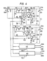
- Fig. 4 shows a more specific embodiment of the present invention
- Fig. 5 illustrates the waveforms of pulses generated in that embodiment.
- the waveshaping circuit 94 is an integrator composed of a resistor 96 and a capacitor 98.
- the output of the integrator is supplied to the base of the transistor 74 in each of the switching regulators 42 to 4N through a capacitor 100.
- the integrator has a time constant selected so as to provide a waveshape having good linearity and peak value properties.
- switching pulses having a waveform as shown in Fig. 5A are generated at the collector of the transistor 56 in the switching regulator 41.
- the waveshaping circuit 94 having the configuration described above shapes these switching pulses into a triangular wave as shown in Fig. 5B. This triangular waveform is supplied to the base of each of the switching regulators 42 to 4N through the capacitor 100.
- control pulses having a waveform as shown in Fig. 5C are provided at the collector of the transistor 74.
- These control pulses are not in phase with the switching pulses shown in Fig. 5A, but the two types of pulses are generated at a synchronous frequency and cause no undesired phenomenon such as beating.
- the waveshaping circuit 94 configured as an integrator requires a minimum number of components and features a very simple circuit design. Furthermore, the use of fewer circuit components contributes to the reduction in the overall size of the power supply device.
- the self-excited switching regulator in association with the waveshaping circuit 94 provides a reference waveform generator circuit for the other switching regulators 42 to 4N, but it should be understood that similar results are obtained if the reference pulses are drawn from the separately excited switching regulators 42 to 4N.
- the power supply device of the present invention permits the use of more than one switching regulator without causing an unwanted beating problem that occurs if the switching regulators do not operate at a synchronous switching frequency.
- the power supply device of the present invention uses only one reference waveform generator and can be manufactured as a compact device.
- the circuit of Fig. 6 has a capacitor 4 and a switching circuit 206 connected between two input terminals 2A and 2B.
- the capacitor 4 removes the ripple component from the input voltage.
- the switching pulses generated in the circuit 206 are supplied to a primary winding 208P of a transformer 208.
- the transformer has secondary windings 208Sa and 208Sb each having a center tap.
- Rectifying diodes 210 and 212 are connected in series between the terminals of the secondary winding 208Sa.
- the cathode of each diode is connected to a common terminal.
- a smoothing capacitor 214 and separately excited switching regulators 216 and 218 are connected between the anode of each diode and the center tap on the secondary winding 208Sa.
- the capacitor terminal on the higher potential side is connected to the collector of a switching transistor 220, and the emitter of this transistor is connected to an output terminal 221A through a choke coil 226.
- the capacitor terminal on the lower potential side is connected to an output terminal 221 B.
- a rectifying diode 228 with the cathode connected to the emitter.
- a smoothing capacitor 230 Between the output terminals 221A and 221B are connected a smoothing capacitor 230 and an error amplifier 232 that detects a variation in the d.c. output.
- the output from the error amplifier 232 is supplied to a pulse width control circuit 234, the controlled pulsating output of which is supplied to the base of the switching transistor 220.
- a waveshaping circuit 236 that shapes the waveform of the switching pulses into a function waveform such as a triangular or sawtooth waveform.
- the output of the circuit 236 is applied as a reference waveform to the pulse width control circuit 234 through a capacitor 238.
- the circuit of Fig. 6 also includes a switching regulator 218 which is configured the same as the switching regulator 216.
- the regulator 218 has a pulse width control circuit that is provided with the output of the waveshaping circuit 236 through a capacitor 240.
- rectifying diodes 242 and 244 are connected in series between the terminals of the secondary winding 208Sb, and the cathode of each diode is connected to a common terminal. Between the cathode of each diode and the center tap on the secondary winding 208Sb are connected a smoothing capacitor 246 and two other switching regulators of the separately excited type 248 and 250.
- the regulators 248 and 250 are configured in the same manner as the switching regulator 216 and are individually provided with the output from the waveshaping circuit 236 through respective capacitors 252 and 254.
- the power supply device having the circuit configuration described above is operated as follows.
- the d.c. voltage supplied across the input terminals 2A and 2B is converted into switching pulses through the circuit 206.
- the switching pulses are supplied to the primary winding 208P of the transformer 208, whereupon the transformed switching pulses are generated on the secondary windings 208Sa and 208Sb.
- the switching pulses generated on the secondary winding 208Sa are supplied to the waveshaping circuit 236, while at the same time, they are subjected to full-wave rectification in the diodes 210 and 212, smoothed in the capacitor 214 and sent to the switching regulators 216 and 218.
- the switching pulses generated on the secondary winding 208Sb are likewise rectified in the diodes 242 and 244, smoothed in the capacitor 246 and supplied to the switching regulators 248 and 250.
- the switching pulses supplied to the waveshaping circuit 236 are converted to a function waveform having a reference waveform such as a triangular or sawtooth wave.
- a reference waveform such as a triangular or sawtooth wave.
- the pulses are shaped into a sawtooth wave and supplied as a reference waveform to the pulse width control circuit 234 in each of the switching regulators 216, 218, 248 and 250.
- the error amplifier 232 checks the output voltage Voa across the terminals 221A and 221B to detect a transient value or a variation in the steady-state value, and the output from the amplifier 232 is supplied to the pulse width control circuit 234 together with the waveshaped switching pulses. This initiates pulse width modulation in the circuit 234 which generates control pulses having an ON-OFF duty ratio adaptive to the detected variation in the d.c. output. These pulses are supplied to the base of the switching transistor 220, which starts a switching operation with a conduction time which suppresses the variation in the d.c. output. As a result of this switching operation, the d.c. voltage from the capacitor 214 is converted to an a.c. voltage, which is rectified and smoothed through the diode 228, choke coil 226 and capacitor 230 and drawn from the output terminals 221A and 221 B as a stabilized d.c. output Voa.
- the switching regulators 216, 218, 248 and 250 operate at a synchronous switching frequency because they receive the same reference waveform as a pulse width control input. The synchronism in the switching frequency prevents the unwanted beating phenomena from occurring in subsequent operation such as signal processing.
- FIG. 7 A specific embodiment of the waveshaping circuit 236 is shown in Fig. 7, wherein the circuit 236 is composed of four integrators 236a, 236b, 236c and 236d connected between one terminal of the secondary winding 208Sa and the center tap. These integrators each include a resistor 256 and a capacitor 258 connected in series between the secondary winding and the tap and they are further connected to the switching regulators 216, 218, 248 and 250, respectively. A sawtooth waveform is generated at the junction between the resistor 256 and capacitor 258 in each integrator and the respective waveforms are individually drawn from capacitors 238, 240, 252 and 254 and supplied to the pulse width control circuit 234 in each switching regulator.
- the desired reference waveform can be easily produced by a very simple circuit configuration.
- One particular advantage is that the amplitude and linearity of the reference waveform can be set at desired values by properly selecting the time constants of the resistor 256 and capacitor 258.
- the waveshaping circuit 236 is composed of four integrators to match the embodiment of Fig. 7, but it should be noted that the same reference waveform can be produced using more integrator circuits so as to be adaptive to an increased number of switching regulators installed in the power supply device.
- Fig. 8 shows another embodiment of the present invention, wherein the variation in the d.c. output is reflected in the switching operation at the input side by connecting the two sides with a photocoupler.
- a ripple absorbing capacitor 4 and a primary winding 266P of a transformer 266 are connected between input terminals 2A and 2B.
- the primary winding 266P is connected in series with a switching transistor 268, which is connected to a pulse width control circuit 270 which then is connected to an error amplifier 274 through a photocoupler 272.
- the transformer has secondary windings 266Sa, 266Sb and 266Sc.
- the waveshaping circuit 236 is connected between the terminals of the secondary windings 266Sa, and one terminal is connected to the anode of a diode 276.
- the cathode of the diode 276 is connected to an output terminal 281A.
- the other terminal of the secondary winding 266Sa is connected to an output terminal 281B.
- a smoothing capacitor 284 and a pair of resistors 286 and 288 for d.c. output detection Between the output terminals 281A and 281B are connected a smoothing capacitor 284 and a pair of resistors 286 and 288 for d.c. output detection.
- the voltage-divided bias that develops at the junction between the resistors 286 and 288 is supplied to the error amplifier 274. Therefore, in the embodiment of Fig. 8, a d.c. voltage Voa is produced at output terminals 281A and 281 B
- the secondary winding 266Sb is connected to a capacitor 292 through a diode 290, and a switching regulator 294 is connected between the two terminals of the capacitor 292.
- the switching regulator 294 is configured as in the embodiment of Fig. 6: the pulse width control circuit 234 is provided with a reference waveform from the waveshaping circuit 236 through a capacitor 296, and the terminals of the capacitor 230 are connected to output terminals 282A and 282B from which a d.c. output Vob is drawn.
- the secondary winding 226Sc is connected to a capacitor 200 through a diode 298, and a switching regulator 202 is connected between the two terminals of the capacitor 200.
- the switching regulator 202 is configured in the same manner as the switching regulator 294: the output of the waveshaping circuit 236 is supplied through a capacitor 204 and a stabilized d.c. voltage Voc is drawn from output terminals 283A and 283B.
- the embodiment of Fig. 8 achieves the same advantages as those obtained with the embodiments of Figs. 6 and 7.
- the waveform of the switching pulses produced on the secondary winding of a transformer is shaped into a function waveform, and this waveform is supplied as an input to the pulse width control circuit in each switching regulator.
- the present invention provides a power supply device that uses a plurality of switching regulators which require a simplified circuit for generating a reference waveform and which can operate at a synchronous switching frequency. The synchronism in the switching frequency prevents unwanted phenomena such as beating from occurring in subsequent operations such as signal processing.
- FIG. 9 A further embodiment of the power supply device of the present invention will now be described by reference to Fig. 9, wherein the device includes a plurality of switching regulators 341, 342, ..., 34N, all of which are of the separately excited type.
- the switching regulator 341 has input terminals 52A and 52B, as well as a ripple absorbing capacitor 54 common to the other switching regulators.
- a d.c. input Vi supplied across the terminals 52A and 52B has its ripple component removed in the capacitor 54.
- the input then is converted to switching pulses in a transistor 56.
- the pulses are rectified in a d.c. reproducing circuit 58 and the resulting d.c. voltage is drawn from output terminals 61A and 61 B as a stabilized d.c. output vo l .
- the d.c. reproducing circuit 58 is composed of a diode 62, a choke coil 64 and a capacitor 66.
- the choke coil 64 is made of a primary winding 64P and a secondary winding 64S. These windings are arranged so as to produce pulses of opposite polarities. One end of each winding is connected to a common terminal, and the other end is connected to the base of the switching transistor 56 through a differentiating capacitor 68, so the switching pulses produced on the secondary winding 64S are fed back to the base of the transistor 56 through the capacitor 68. Therefore, differential pulses coming out of the capacitor 68 are in synchronism with the switching pulses, and in order to shorten the switching time of the transistor 56, those pulses are superimposed on control pulses issued from transistor 74.
- a bias resistor 70 is connected between the base and emitter of the transistor 56. Between the base of that transistor and the output of the d.c. reproducing circuit 58 is connected a transistor 74 through a resistor 72, with the collector connected to the base of the transistor 56 and the emitter to the output of the d.c. reproducing circuit.
- the base of the transistor 74 is provided with a bias from the d.c. input through a resistor 82.
- the base of the transistor 74 is also connected to the collector of transistor 84 for controlling the operating current flowing through the transistor 74.
- the emitter of the transistor 84 is connected to a constant-voltage diode (Zener diode) 86 for providing a reference voltage with the anode connected to ground.
- the emitter of the transistor 84 is also provided with the reproduced d.c. output through a resistor 88.
- the base of the transistor 84 is provided with the d.c. output Vo, after it is voltage-divided at the junction between resistors 90 and 92 connected in series between the output terminals 61A and 61 B.
- the voltage-divided bias is compared with the reference voltage which is the sum of the zener voltage on the diode 86 and the voltage across the base and emitter of the transistor 84.
- Switching regulators 342 to 34N have the same circuit configuration as the switching regulator 341 and are so designed that stabilized outputs Vo2 to V On are drawn from respective pairs of output terminals 362A/362B to 36NA/36NB.
- the switching regulators 341, 342,..., 34N have one common waveform generator circuit 396 that generates a reference function wave such as a triangular or sawtooth wave.
- the reference waveforms produced from the circuit 396 are supplied to the base of transistors 74 in switching regulators 341, 342, ... , 34N through respective capacitors 301, 302, ... , 30N. These waveforms are superimposed on the operating output from the transistor 74. Therefore, the common waveform generator 396 provides a pulse width modulating circuit together with the transistors 74 and 84 in each of the switching regulators 341, 342, ... , 34N.
- the power supply device having the circuit configuration described above is operated as follows.
- the reference waveform from the waveform generator 396 is supplied to the base of the transistor 74
- the superposition of that waveform on the waveform of the operating output from the transistor 84 initiates a pulse width modulation.
- This provides a control on the current flowing to the base of the transistor 74. Since this control depends on the d.c. output, the control pulses supplied from the transistor 74 to the base of the transistor 56 constitute a pulsating signal whose pulse width is modulated depending upon the variation in the level of the d.c. output.
- the transistor 56 performs a switching operation at an ON-OFF duty ratio that suppresses the variation in the d.c. output level.
- This control operation is performed continuously: the d.c. input supplied across the terminals 52A and 52B is passed through the transistor 56 where it is converted into switching pulses, which are rectified in the d.c. reproducing circuit 58 and are drawn from the output terminals 61A and 61 B as a stabilized output Vo l . If there occurs a variation in the d.c. input on account of load fluctuation or other factors, the switching regulator 341 of the present invention achieves the intended stabilizing and controlling operation momentarily and thus keeps supplying a constant d.c. output to the load.
- the switching pulses that develop at the collector of the transistor 56 as a result of its switching operation are applied to the primary winding 64P of the choke coil 64, and the secondary winding 64S produces pulses having a polarity reversed from those applied to the primary winding.
- the induced pulses are differentiated in the capacitor 68 and are fed to the base of the switching transistor 56.
- the respective edges of the differential pulses are in good agreement with those of the initial switching pulses, and the leading and trailing edges of each pulse change their potential levels in opposite directions. Therefore, the differential pulses are timed to the switching operation of the transistor 56 and can accelerate the turning-on and off of that transistor, as described above.
- the switching time of the transistor 56 is shortened, and at the same time, the transistor 56 produces sharp-edged pulses having short rise and fall times. In consequence, the power loss occurring in the switching period can be reduced and the transducing effieincy of the switching regulator 341 is increased.
- Similar pulse width control is performed in the switching regulators 342 to 34N: the d.c. input supplied across the terminals 52A and 52B is converted to switching pulses in the transistor 56, and after these pulses are rectified in the d.c. reproducing circuit 58, stabilized d.c. outputs Vo 2 to Vo n are drawn from the respective output channels.
- one common reference waveform is used in performing pulse width control in each of the switching regulators 341, 342, ... , 34N, where the regulators can be operated at a synchronous switching frequency. Therefore, unlike the conventional system using a reference wave generator for each switching regulator, the power supply device of the present invention is free from the beating problem that may occur due to the switching at different frequencies. As an obvious advantage, the use of a single reference waveform generator in the entire system provides a power supply device of a very simple design.
- the power supply device of the present invention permits the use of more than one switching regulator without causing the beating phenomena that occurs if the switching regulators do not operate at a synchronous switching frequency.
- the power supply device of the present invention uses only one reference waveform generator and can be manufactured as a compact device.
Description
- The present invention relates to a power supply device, and more particularly, to a power supply device including a plurality of switching regulators which are synchronized with each other in their switching frequency.
- Most electronic devices such as video tape recorders (VTR) and video cameras, whether portable or installed on vehicles or the like, use batteries for driving power. But the terminal voltage of batteries may vary greatly when there occurs a sudden change in the load as a result of mode switching. To suppress these variations and stabilize the operation of the electronic devices, stabilizing power suppliers are currently used. These power supply devices use a switching regulator, and to provide an output voltage adaptive to more than one load, a plurality of switching regulators are necessary.
- Fig. 1 shows a conventional separately excited switching regulator used in the power supply device contemplated by the present invention. A d.c. input Vi supplied across
input terminals capacitor 4 provided between the two input terminals. The input then is converted to an a.c. voltage in a switching transistor 6. The a.c. voltage is rectified in a d.c. reproducingcircuit 14 composed of adiode 8, achoke coil 10 and acapacitor 12. Subsequently, the d.c. voltage is drawn fromoutput terminals - For drawing a voltage-divided bias from the d.c. output voltage Vo,
resistors terminals resistors error amplifier 22 where it is compared with a reference voltage provided by areference power supply 24. The detected difference is fed to the non-inverting input terminal of acomparator 26, and an output comprising triangular waves as shown in Fig. 2A from a reference wave generator circuit is supplied to the inverting input terminal of thecomparator 26. In Fig. 2A, the varying output produced from theerror amplifier 22 is denoted by Ve. Given the two inputs, thecomparator 26 performs a pulse width modulating operation and generates pulses whose width is controlled by the varying output V as shown in Fig. 2B. These pulses are fed to atransistor 30 as a control input, and in response to the switching operation of thetransistor 30, a pulsating drive current flows into the switching transistor 6 through aresistor 32 and, thus, the transistor 6 performs a switching operation. Abias resistor 34 is connected between the emitter and base of the switching transistor 6. - If a plurality of switching regulators having the above-described circuit configuration are assembled to make up a power supply device, a reference wave generator is necessary for each switching regulator. This first of all makes the overall configuration of the power supply device complex. In addition, if the oscillating frequencies of the individual generator circuits are not in synchronism with each other, serious beating may occur, and this phenomenon must be prevented by all means because it produces a noise problem and can cause incorrect operation during the oscillation and signal processing in internal circuits of VTR or video cameras. The same problem occurs if the regulators used are of a self-excited switching type having respective oscillation control units.
- Therefore, an object of the present invention is to provide a power supply device including a plurality of switching regulators which are synchronized in the operation of pulse width control units and which use one common reference wave generator to simplify the overall design of the device.
- This object can be achieved by a power supply device, comprising a plurality of switching regulators, and a waveshaping circuit for deriving a periodic reference waveform from the switching pulses generated within one of said switching regulators and for supplying this periodic reference waveform to the others of said switching regulators in which it is compared with a signal derived from a mean value of the respective output voltage in order to individually control the pulse width of the output voltages of the other switching regulators.
- Further, this object can be achieved by a power supply device, comprising a plurality of switching regulators, the pulse width of their output voltage pulses being separately controlled by comparing a signal derived from a mean value of the respective output voltage with a periodic reference waveform which is provided by a common waveform generator and separately delivered to the switching regulators.
- This invention can be more fully understood from the following detailed description when taken in conjunction with the accompanying drawings, in which:
- Fig. 1 is a circuit diagram showing a conventional switching regulator;
- Fig. 2 is a diagram showing the waveform of pulses produced by the switching regulator of Fig. 1;
- Fig. 3 is a circuit diagram showing an embodiment of the power supply device of the present invention;
- Fig. 4 is a circuit diagram showing a specific embodiment of the power supply device of the present invention;
- Fig. 5 is a diagram showing the waveforms of pulses produced in the power supply device of Fig. 4;
- Fig. 6 is a circuit diagram showing another embodiment of the power supply device of the present invention;
- Fig. 7 is a circuit diagram showing an embodiment of the waveshaping circuit used in the power supply device of Fig. 6;
- Fig. 8 is a circuit diagram showing still another embodiment of the present invention; and
- Fig. 9 is a circuit diagram showing one embodiment of the power supply device of the present invention.
- A first embodiment of the power supply device of the present invention is hereunder described by reference to Fig. 3, wherein the device includes a plurality of
switching regulators - The
switching regulator 41 hasinput terminals ripple absorbing capacitor 54 common to the other switching regulators. A d.c. input Vi supplied across theterminals capacitor 54. The input then is converted to switching pulses in atransistor 56. The pulses are rectified in a d.c. reproducingcircuit 58 and the resulting d.c. voltage is drawn fromoutput terminals circuit 58 is composed of adiode 62, achoke coil 64 and acapacitor 66. In the embodiment shown, thechoke coil 64 is made of a primary winding 64P and asecondary winding 64S. These windings are arranged so that they produce pulses of opposite polarities. The switching pulses produced by the secondary winding 64S are fed back to the base of theswitching transistor 56 through a differentiatingcapacitor 68. The differential pulses coming out of thecapacitor 68 are in synchronism with the switching pulses, and in order to shorten the switching time of thetransistor 56, these pulses are added to the base of thetransistor 56 after being superimposed on control pulses issued from atransistor 74 to be described later. - A
bias resistor 70 is connected between the base and emitter of thetransistor 56. Between the base of that transistor and the output of the d.c. reproducingcircuit 58 is connected atransistor 74 through aresistor 72, with the collector connected to the base of thetransistor 56 and the emitter to the d.c. reproducing circuit. Afeedback circuit 80 including acapacitor 76 connected in series with a resistor 78 is provided between the base of thetransistor 74 and the collector of theswitching transistor 56. The base of thetransistor 74 is provided with a bias from the d.c. input through aresistor 82. When the base of thetransistor 74 is provided with a signal returned from the collector of the switchingtransistor 56 through thepositive feedback circuit 80, thetransistor 74 starts to oscillate and functions as a pulse width controlling oscillator that provides a drive current for thetransistor 56. At the same time, thetransistor 74 is capable of adding such drive current onto the reproduced d.c. output from thecircuit 58. - The base of the
transistor 74 is also connected to the collector of atransistor 84 for controlling the operating current flowing throughtransistor 74. The emitter of thetransistor 84 is connected to a constant-voltage diode (Zener diode) 86 for providing a reference voltage, with the anode connected to ground. The emitter of thetransistor 84 is also provided with the reproduced d.c. output through aresistor 88. The base of thetransistor 84 is provided with the d.c. output after it is voltage-divided at the junction betweenresistors output terminals 61A and 61 B. In thetransistor 84, voltage-divided bias is compared with the reference voltage which is the sum of the zener voltage on thediode 86 and the voltage across the base and emitter of thetransistor 84. -
Switching regulators 42 to 4N have the same circuit configuration as the switchingregulator 41 except that they do not include thefeedback circuit 80. They are designed so that stabilized outputs V02 to Von are drawn from respective pairs ofoutput terminals - The switching pulses formed by the
transistor 56 in the switchingregulator 41 are drawn from the collector of that transistor and fed to awaveshaping circuit 94. Thewaveshaping circuit 94 enables the switchingregulator 41 to function as a conventional reference waveform generator circuit with respect to the switchingregulators 42 to 4N. For this purpose, the circuit is designed so that it shapes the switching pulses into the waveform of a reference function such as a triangular or sawtooth wave. The reference waveform generated by thewaveshaping circuit 94 is sent to the base of atransistor 74 in each of the switchingregulators 42 to 4N. - The device having the circuit configuration described above is operated as follows. The
transistor 74 for providing a drive current through the switchingtransistor 56 starts to oscillate when the switching pulses formed by thetransistor 56 are positively fed back to the base of thetransistor 74. The current flowing to the base of the oscillatingtransistor 74 is controlled by thetransistor 84, and this controlling operation of thetransistor 84 depends on the d.c. output. Therefore, the control pulses supplied to the base of thetransistor 56 upon oscillation of thetransistor 74 constitute a pulsating signal whose pulse width is modulated depending upon the variation in the level of the d.c. output. In consequence, thetransistor 56 performs a switching operation. - This control operation is performed continuously: the d.c. input supplied across the
terminals transistor 56 where it is converted into switching pulses, which are rectified in the d.c. reproducingcircuit 58 and are drawn from theoutput terminals regulator 41 of the present invention achieves the intended stabilizing and controlling operation momentarily and thus keeps supplying a constant d.c. output to the load. - The switching pulses that develop at the collector of the
transistor 56 as a result of its switching operation are applied to the primary winding 64P of thechoke coil 64, and the secondary winding 64S produces pulses having their polarity reversed from those applied to the primary winding. The induced pulses are differentiated in thecapacitor 68 and are fed to the base of thetransistor 56. The respective edges of the differential pulses are in good agreement with those of the initial switching pulses, and the leading and trailing edges of each pulse change their potential levels in opposite directions. Therefore, the differential pulses are timed to the switching operation of thetransistor 56 and can accelerate the turning-on and off of that transistor. As a result, the switching time of thetransistor 56 is shortened, and at the same time, thetransistor 56 produces sharp-edged pulses having short rise and fall times. In consequence, the power loss occurring in the switching period can be reduced and the transducing efficiency of the switchingregulator 41 is increased. - The switching pulses produced at the collector of the
transistor 56 are fed to thewaveshaping circuit 94 where they are shaped to a reference waveform such as a triangular or sawtooth wave. This reference wave is supplied as a pulse width control input to the base of thetransistor 74 in each of the separatedly excited switchingregulators 42 to 4N, and this control input enables the switchingregulators 42 to 4N to perform similar pulse width controlling operations as in the switching regulator 41: the d.c. input applied across theterminals transistor 56, and after they are rectified in the d.c. reproducingcircuit 58, stabilized d.c. outputs V02 to Von are drawn from the respective output channels. - As described above, the switching
regulators 42 to 4N are provided with pulses in a reference waveform that have been obtained by shaping the switching pulses produced by thetransistor 56 in the switchingregulator 41, and thus the respective switching regulators are operated at a synchronous switching frequency. Therefore, unlike the conventional system wherein each switching regulator had its own reference wave generating circuit, the power supply device of the present invention is free from the beating problem that occurred due to switching at different frequencies. As an obvious advantage, the use of a single reference waveform generator in the entire system provides a power supply device of a very simple design. - Fig. 4 shows a more specific embodiment of the present invention, and Fig. 5 illustrates the waveforms of pulses generated in that embodiment. In this embodiment, the
waveshaping circuit 94 is an integrator composed of aresistor 96 and acapacitor 98. The output of the integrator is supplied to the base of thetransistor 74 in each of the switchingregulators 42 to 4N through acapacitor 100. The integrator has a time constant selected so as to provide a waveshape having good linearity and peak value properties. - Suppose switching pulses having a waveform as shown in Fig. 5A are generated at the collector of the
transistor 56 in the switchingregulator 41. Thewaveshaping circuit 94 having the configuration described above shapes these switching pulses into a triangular wave as shown in Fig. 5B. This triangular waveform is supplied to the base of each of the switchingregulators 42 to 4N through thecapacitor 100. If the control level provided by thetransistor 74 is indicated by Vd in Fig. 5B, control pulses having a waveform as shown in Fig. 5C are provided at the collector of thetransistor 74. These control pulses are not in phase with the switching pulses shown in Fig. 5A, but the two types of pulses are generated at a synchronous frequency and cause no undesired phenomenon such as beating. - As shown above, the
waveshaping circuit 94 configured as an integrator requires a minimum number of components and features a very simple circuit design. Furthermore, the use of fewer circuit components contributes to the reduction in the overall size of the power supply device. - In the embodiment shown above, the self-excited switching regulator in association with the
waveshaping circuit 94 provides a reference waveform generator circuit for the other switchingregulators 42 to 4N, but it should be understood that similar results are obtained if the reference pulses are drawn from the separately excited switchingregulators 42 to 4N. - As will be understood from the foregoing description, the power supply device of the present invention permits the use of more than one switching regulator without causing an unwanted beating problem that occurs if the switching regulators do not operate at a synchronous switching frequency. As further advantages, the power supply device of the present invention uses only one reference waveform generator and can be manufactured as a compact device.
- A further embodiment of the power supply device of the present invention will now be described by reference to Fig. 6. The circuit of Fig. 6 has a
capacitor 4 and aswitching circuit 206 connected between twoinput terminals capacitor 4 removes the ripple component from the input voltage. The switching pulses generated in thecircuit 206 are supplied to a primary winding 208P of atransformer 208. The transformer has secondary windings 208Sa and 208Sb each having a center tap. - Rectifying
diodes capacitor 214 and separately excited switchingregulators transistor 220, and the emitter of this transistor is connected to anoutput terminal 221A through achoke coil 226. The capacitor terminal on the lower potential side is connected to an output terminal 221 B. Between theoutput terminal 221 B and the emitter of the switchingtransistor 220 is connected a rectifyingdiode 228 with the cathode connected to the emitter. Between theoutput terminals capacitor 230 and anerror amplifier 232 that detects a variation in the d.c. output. The output from theerror amplifier 232 is supplied to a pulsewidth control circuit 234, the controlled pulsating output of which is supplied to the base of the switchingtransistor 220. - Between the tap on the secondary winding 208Sa and its terminal on the anode side is connected a
waveshaping circuit 236 that shapes the waveform of the switching pulses into a function waveform such as a triangular or sawtooth waveform. The output of thecircuit 236 is applied as a reference waveform to the pulsewidth control circuit 234 through acapacitor 238. - The circuit of Fig. 6 also includes a
switching regulator 218 which is configured the same as theswitching regulator 216. Theregulator 218 has a pulse width control circuit that is provided with the output of thewaveshaping circuit 236 through acapacitor 240. - In the embodiment of Fig. 6, rectifying
diodes 242 and 244 are connected in series between the terminals of the secondary winding 208Sb, and the cathode of each diode is connected to a common terminal. Between the cathode of each diode and the center tap on the secondary winding 208Sb are connected a smoothingcapacitor 246 and two other switching regulators of the separatelyexcited type regulators switching regulator 216 and are individually provided with the output from thewaveshaping circuit 236 throughrespective capacitors - The power supply device having the circuit configuration described above is operated as follows. The d.c. voltage supplied across the
input terminals circuit 206. The switching pulses are supplied to the primary winding 208P of thetransformer 208, whereupon the transformed switching pulses are generated on the secondary windings 208Sa and 208Sb. The switching pulses generated on the secondary winding 208Sa are supplied to thewaveshaping circuit 236, while at the same time, they are subjected to full-wave rectification in thediodes capacitor 214 and sent to the switchingregulators diodes 242 and 244, smoothed in thecapacitor 246 and supplied to the switchingregulators - The switching pulses supplied to the
waveshaping circuit 236 are converted to a function waveform having a reference waveform such as a triangular or sawtooth wave. In the embodiment shown, the pulses are shaped into a sawtooth wave and supplied as a reference waveform to the pulsewidth control circuit 234 in each of the switchingregulators - In the
switching regulator 216, theerror amplifier 232 checks the output voltage Voa across theterminals amplifier 232 is supplied to the pulsewidth control circuit 234 together with the waveshaped switching pulses. This initiates pulse width modulation in thecircuit 234 which generates control pulses having an ON-OFF duty ratio adaptive to the detected variation in the d.c. output. These pulses are supplied to the base of the switchingtransistor 220, which starts a switching operation with a conduction time which suppresses the variation in the d.c. output. As a result of this switching operation, the d.c. voltage from thecapacitor 214 is converted to an a.c. voltage, which is rectified and smoothed through thediode 228,choke coil 226 andcapacitor 230 and drawn from theoutput terminals - The above operations, which are momentarily effected and continuously repeated are also carried out simultaneously in the other switching
regulators output terminals 222A/222B, 223A/223B, and 224A/224B. - In the stabilizing operation described above, no special circuit for generating a reference waveform is necessary except for the
waveshaping circuit 236 that shapes the switching pulses produced in the secondary winding 208Sa of the transformer. Furthermore, the switchingregulators - A specific embodiment of the
waveshaping circuit 236 is shown in Fig. 7, wherein thecircuit 236 is composed of fourintegrators resistor 256 and acapacitor 258 connected in series between the secondary winding and the tap and they are further connected to the switchingregulators resistor 256 andcapacitor 258 in each integrator and the respective waveforms are individually drawn fromcapacitors width control circuit 234 in each switching regulator. In this way, the desired reference waveform can be easily produced by a very simple circuit configuration. One particular advantage is that the amplitude and linearity of the reference waveform can be set at desired values by properly selecting the time constants of theresistor 256 andcapacitor 258. In the embodiment shown, thewaveshaping circuit 236 is composed of four integrators to match the embodiment of Fig. 7, but it should be noted that the same reference waveform can be produced using more integrator circuits so as to be adaptive to an increased number of switching regulators installed in the power supply device. - Fig. 8 shows another embodiment of the present invention, wherein the variation in the d.c. output is reflected in the switching operation at the input side by connecting the two sides with a photocoupler. As in the embodiment of Fig. 6, a
ripple absorbing capacitor 4 and a primary winding 266P of atransformer 266 are connected betweeninput terminals transistor 268, which is connected to a pulsewidth control circuit 270 which then is connected to anerror amplifier 274 through aphotocoupler 272. - The transformer has secondary windings 266Sa, 266Sb and 266Sc. The
waveshaping circuit 236 is connected between the terminals of the secondary windings 266Sa, and one terminal is connected to the anode of adiode 276. The cathode of thediode 276 is connected to anoutput terminal 281A. Likewise, the other terminal of the secondary winding 266Sa is connected to anoutput terminal 281B. Between theoutput terminals capacitor 284 and a pair ofresistors resistors error amplifier 274. Therefore, in the embodiment of Fig. 8, a d.c. voltage Voa is produced atoutput terminals - The secondary winding 266Sb is connected to a
capacitor 292 through adiode 290, and aswitching regulator 294 is connected between the two terminals of thecapacitor 292. Theswitching regulator 294 is configured as in the embodiment of Fig. 6: the pulsewidth control circuit 234 is provided with a reference waveform from thewaveshaping circuit 236 through acapacitor 296, and the terminals of thecapacitor 230 are connected tooutput terminals - In a similar manner, the secondary winding 226Sc is connected to a
capacitor 200 through adiode 298, and aswitching regulator 202 is connected between the two terminals of thecapacitor 200. Theswitching regulator 202 is configured in the same manner as the switching regulator 294: the output of thewaveshaping circuit 236 is supplied through acapacitor 204 and a stabilized d.c. voltage Voc is drawn fromoutput terminals - As described above, the waveform of the switching pulses produced on the secondary winding of a transformer is shaped into a function waveform, and this waveform is supplied as an input to the pulse width control circuit in each switching regulator. Because of this arrangement, the present invention provides a power supply device that uses a plurality of switching regulators which require a simplified circuit for generating a reference waveform and which can operate at a synchronous switching frequency. The synchronism in the switching frequency prevents unwanted phenomena such as beating from occurring in subsequent operations such as signal processing.
- A further embodiment of the power supply device of the present invention will now be described by reference to Fig. 9, wherein the device includes a plurality of switching
regulators - The
switching regulator 341 hasinput terminals ripple absorbing capacitor 54 common to the other switching regulators. A d.c. input Vi supplied across theterminals capacitor 54. The input then is converted to switching pulses in atransistor 56. The pulses are rectified in a d.c. reproducingcircuit 58 and the resulting d.c. voltage is drawn fromoutput terminals circuit 58 is composed of adiode 62, achoke coil 64 and acapacitor 66. In the embodiment shown, thechoke coil 64 is made of a primary winding 64P and a secondary winding 64S. These windings are arranged so as to produce pulses of opposite polarities. One end of each winding is connected to a common terminal, and the other end is connected to the base of the switchingtransistor 56 through a differentiatingcapacitor 68, so the switching pulses produced on the secondary winding 64S are fed back to the base of thetransistor 56 through thecapacitor 68. Therefore, differential pulses coming out of thecapacitor 68 are in synchronism with the switching pulses, and in order to shorten the switching time of thetransistor 56, those pulses are superimposed on control pulses issued fromtransistor 74. - A
bias resistor 70 is connected between the base and emitter of thetransistor 56. Between the base of that transistor and the output of the d.c. reproducingcircuit 58 is connected atransistor 74 through aresistor 72, with the collector connected to the base of thetransistor 56 and the emitter to the output of the d.c. reproducing circuit. The base of thetransistor 74 is provided with a bias from the d.c. input through aresistor 82. The base of thetransistor 74 is also connected to the collector oftransistor 84 for controlling the operating current flowing through thetransistor 74. The emitter of thetransistor 84 is connected to a constant-voltage diode (Zener diode) 86 for providing a reference voltage with the anode connected to ground. The emitter of thetransistor 84 is also provided with the reproduced d.c. output through aresistor 88. The base of thetransistor 84 is provided with the d.c. output Vo, after it is voltage-divided at the junction betweenresistors output terminals 61A and 61 B. In thetransistor 84, the voltage-divided bias is compared with the reference voltage which is the sum of the zener voltage on thediode 86 and the voltage across the base and emitter of thetransistor 84. -
Switching regulators 342 to 34N have the same circuit configuration as theswitching regulator 341 and are so designed that stabilized outputs Vo2 to VOn are drawn from respective pairs ofoutput terminals 362A/362B to 36NA/36NB. - The switching
regulators waveform generator circuit 396 that generates a reference function wave such as a triangular or sawtooth wave. The reference waveforms produced from thecircuit 396 are supplied to the base oftransistors 74 in switchingregulators respective capacitors transistor 74. Therefore, thecommon waveform generator 396 provides a pulse width modulating circuit together with thetransistors regulators - The power supply device having the circuit configuration described above is operated as follows. When the reference waveform from the
waveform generator 396 is supplied to the base of thetransistor 74, the superposition of that waveform on the waveform of the operating output from thetransistor 84 initiates a pulse width modulation. This provides a control on the current flowing to the base of thetransistor 74. Since this control depends on the d.c. output, the control pulses supplied from thetransistor 74 to the base of thetransistor 56 constitute a pulsating signal whose pulse width is modulated depending upon the variation in the level of the d.c. output. In consequence, thetransistor 56 performs a switching operation at an ON-OFF duty ratio that suppresses the variation in the d.c. output level. - This control operation is performed continuously: the d.c. input supplied across the
terminals transistor 56 where it is converted into switching pulses, which are rectified in the d.c. reproducingcircuit 58 and are drawn from theoutput terminals switching regulator 341 of the present invention achieves the intended stabilizing and controlling operation momentarily and thus keeps supplying a constant d.c. output to the load. - The switching pulses that develop at the collector of the
transistor 56 as a result of its switching operation are applied to the primary winding 64P of thechoke coil 64, and the secondary winding 64S produces pulses having a polarity reversed from those applied to the primary winding. The induced pulses are differentiated in thecapacitor 68 and are fed to the base of the switchingtransistor 56. The respective edges of the differential pulses are in good agreement with those of the initial switching pulses, and the leading and trailing edges of each pulse change their potential levels in opposite directions. Therefore, the differential pulses are timed to the switching operation of thetransistor 56 and can accelerate the turning-on and off of that transistor, as described above. As a result, the switching time of thetransistor 56 is shortened, and at the same time, thetransistor 56 produces sharp-edged pulses having short rise and fall times. In consequence, the power loss occurring in the switching period can be reduced and the transducing effieincy of theswitching regulator 341 is increased. - Similar pulse width control is performed in the switching
regulators 342 to 34N: the d.c. input supplied across theterminals transistor 56, and after these pulses are rectified in the d.c. reproducingcircuit 58, stabilized d.c. outputs Vo2 to Von are drawn from the respective output channels. - As a particular advantage, one common reference waveform is used in performing pulse width control in each of the switching
regulators - As will be understood from the foregoing description, the power supply device of the present invention permits the use of more than one switching regulator without causing the beating phenomena that occurs if the switching regulators do not operate at a synchronous switching frequency. As further advantages, the power supply device of the present invention uses only one reference waveform generator and can be manufactured as a compact device.
Claims (5)
Priority Applications (1)
| Application Number | Priority Date | Filing Date | Title |
|---|---|---|---|
| AT83105465T ATE25450T1 (en) | 1982-06-04 | 1983-06-01 | POWER SUPPLY DEVICE. |
Applications Claiming Priority (6)
| Application Number | Priority Date | Filing Date | Title |
|---|---|---|---|
| JP57095980A JPS58215927A (en) | 1982-06-04 | 1982-06-04 | Power source |
| JP95980/82 | 1982-06-04 | ||
| JP123342/82U | 1982-08-14 | ||
| JP12334282U JPS5928281U (en) | 1982-08-14 | 1982-08-14 | power supply |
| JP154882/82 | 1982-09-06 | ||
| JP15488282A JPS5944969A (en) | 1982-09-06 | 1982-09-06 | Power source |
Publications (2)
| Publication Number | Publication Date |
|---|---|
| EP0096370A1 EP0096370A1 (en) | 1983-12-21 |
| EP0096370B1 true EP0096370B1 (en) | 1987-02-04 |
Family
ID=27307964
Family Applications (1)
| Application Number | Title | Priority Date | Filing Date |
|---|---|---|---|
| EP83105465A Expired EP0096370B1 (en) | 1982-06-04 | 1983-06-01 | Power supply device |
Country Status (3)
| Country | Link |
|---|---|
| US (1) | US4538101A (en) |
| EP (1) | EP0096370B1 (en) |
| DE (1) | DE3369778D1 (en) |
Families Citing this family (51)
| Publication number | Priority date | Publication date | Assignee | Title |
|---|---|---|---|---|
| DE3323905A1 (en) * | 1983-07-02 | 1985-01-10 | ANT Nachrichtentechnik GmbH, 7150 Backnang | CIRCUIT ARRANGEMENT FOR DETECTING A CURRENT IN POWER SUPPLY DEVICES |
| GB8405520D0 (en) * | 1984-03-02 | 1984-04-04 | Alcan Int Ltd | Electrical power control |
| FR2565434A1 (en) * | 1984-05-30 | 1985-12-06 | Inf Milit Spatiale Aeronaut | POWER CUTTING POWER SUPPLY |
| US4766364A (en) * | 1987-11-04 | 1988-08-23 | International Business Machines Corporation | Parallel power systems |
| US5399956A (en) * | 1992-02-03 | 1995-03-21 | Motorola, Inc. | Backup battery system for a portable electronic device |
| US5355077A (en) * | 1992-04-27 | 1994-10-11 | Dell U.S.A., L.P. | High efficiency regulator with shoot-through current limiting |
| US5399908A (en) * | 1992-06-26 | 1995-03-21 | Kollmorgen Corporation | Apparatus and method for forced sharing of parallel MOSFET switching losses |
| US5377090A (en) * | 1993-01-19 | 1994-12-27 | Martin Marietta Corporation | Pulsed power converter with multiple output voltages |
| JP2574261Y2 (en) * | 1993-09-01 | 1998-06-11 | ヤマハ株式会社 | Switching power supply circuit |
| US5841313A (en) * | 1995-08-30 | 1998-11-24 | Cherry Semiconductor Corporation | Switch with programmable delay |
| US5757210A (en) * | 1995-08-30 | 1998-05-26 | Cherry Semiconductor Corporation | Comparator with latch |
| US5805401A (en) * | 1995-08-30 | 1998-09-08 | Cherry Semiconductor Corporation | Undervoltage lockout circuit with sleep pin |
| US5781058A (en) * | 1995-08-30 | 1998-07-14 | Cherry Semiconductor Corporation | Totem pole driver with cross conduction protection and default low impedance state output |
| US5793241A (en) * | 1995-11-30 | 1998-08-11 | Cherry Semiconductor Corporation | High speed active op-amp clamp |
| JPH09215319A (en) * | 1996-02-01 | 1997-08-15 | Toyota Autom Loom Works Ltd | Dc-dc converter |
| JP3384521B2 (en) * | 1996-06-07 | 2003-03-10 | 矢崎総業株式会社 | Switching device |
| US7269034B2 (en) | 1997-01-24 | 2007-09-11 | Synqor, Inc. | High efficiency power converter |
| US5912552A (en) * | 1997-02-12 | 1999-06-15 | Kabushiki Kaisha Toyoda Jidoshokki Seisakusho | DC to DC converter with high efficiency for light loads |
| JPH10313572A (en) * | 1997-05-09 | 1998-11-24 | Toyota Autom Loom Works Ltd | Switching regulator control system |
| ATE191572T1 (en) * | 1997-07-18 | 2000-04-15 | Ansaldo Sistemi Spa | ELECTRONIC CIRCUIT FOR TRANSIENT REDUCTION WHEN SWITCHING ON |
| US5990668A (en) * | 1997-11-07 | 1999-11-23 | Sierra Applied Sciences, Inc. | A.C. power supply having combined regulator and pulsing circuits |
| US6058034A (en) * | 1998-10-19 | 2000-05-02 | Dell Usa Lp | Current converter and source identification and detection |
| US7000125B2 (en) * | 2002-12-21 | 2006-02-14 | Power-One, Inc. | Method and system for controlling and monitoring an array of point-of-load regulators |
| US6949916B2 (en) | 2002-11-12 | 2005-09-27 | Power-One Limited | System and method for controlling a point-of-load regulator |
| US7049798B2 (en) * | 2002-11-13 | 2006-05-23 | Power-One, Inc. | System and method for communicating with a voltage regulator |
| US7394445B2 (en) | 2002-11-12 | 2008-07-01 | Power-One, Inc. | Digital power manager for controlling and monitoring an array of point-of-load regulators |
| US7456617B2 (en) | 2002-11-13 | 2008-11-25 | Power-One, Inc. | System for controlling and monitoring an array of point-of-load regulators by a host |
| US6833691B2 (en) | 2002-11-19 | 2004-12-21 | Power-One Limited | System and method for providing digital pulse width modulation |
| US6933709B2 (en) * | 2003-02-10 | 2005-08-23 | Power-One Limited | Digital control system and method for switched mode power supply |
| US7882372B2 (en) | 2002-12-21 | 2011-02-01 | Power-One, Inc. | Method and system for controlling and monitoring an array of point-of-load regulators |
| US7836322B2 (en) | 2002-12-21 | 2010-11-16 | Power-One, Inc. | System for controlling an array of point-of-load regulators and auxiliary devices |
| US7249267B2 (en) * | 2002-12-21 | 2007-07-24 | Power-One, Inc. | Method and system for communicating filter compensation coefficients for a digital power control system |
| US7673157B2 (en) | 2002-12-21 | 2010-03-02 | Power-One, Inc. | Method and system for controlling a mixed array of point-of-load regulators through a bus translator |
| US7266709B2 (en) | 2002-12-21 | 2007-09-04 | Power-One, Inc. | Method and system for controlling an array of point-of-load regulators and auxiliary devices |
| US7737961B2 (en) | 2002-12-21 | 2010-06-15 | Power-One, Inc. | Method and system for controlling and monitoring an array of point-of-load regulators |
| US7743266B2 (en) | 2002-12-21 | 2010-06-22 | Power-One, Inc. | Method and system for optimizing filter compensation coefficients for a digital power control system |
| US7373527B2 (en) | 2002-12-23 | 2008-05-13 | Power-One, Inc. | System and method for interleaving point-of-load regulators |
| US7710092B2 (en) | 2003-02-10 | 2010-05-04 | Power-One, Inc. | Self tracking ADC for digital power supply control systems |
| US7023190B2 (en) * | 2003-02-10 | 2006-04-04 | Power-One, Inc. | ADC transfer function providing improved dynamic regulation in a switched mode power supply |
| US7080265B2 (en) | 2003-03-14 | 2006-07-18 | Power-One, Inc. | Voltage set point control scheme |
| US6936999B2 (en) * | 2003-03-14 | 2005-08-30 | Power-One Limited | System and method for controlling output-timing parameters of power converters |
| US6788036B1 (en) | 2003-03-28 | 2004-09-07 | Ower-One Limited | Method and system for current sharing among a plurality of power modules |
| US6958592B2 (en) * | 2003-11-26 | 2005-10-25 | Power-One, Inc. | Adaptive delay control circuit for switched mode power supply |
| US7372682B2 (en) * | 2004-02-12 | 2008-05-13 | Power-One, Inc. | System and method for managing fault in a power system |
| US20050286709A1 (en) * | 2004-06-28 | 2005-12-29 | Steve Horton | Customer service marketing |
| US7141956B2 (en) * | 2005-03-18 | 2006-11-28 | Power-One, Inc. | Digital output voltage regulation circuit having first control loop for high speed and second control loop for high accuracy |
| US7554310B2 (en) | 2005-03-18 | 2009-06-30 | Power-One, Inc. | Digital double-loop output voltage regulation |
| US7239115B2 (en) * | 2005-04-04 | 2007-07-03 | Power-One, Inc. | Digital pulse width modulation controller with preset filter coefficients |
| US7327149B2 (en) * | 2005-05-10 | 2008-02-05 | Power-One, Inc. | Bi-directional MOS current sense circuit |
| US7834613B2 (en) | 2007-10-30 | 2010-11-16 | Power-One, Inc. | Isolated current to voltage, voltage to voltage converter |
| US10199950B1 (en) | 2013-07-02 | 2019-02-05 | Vlt, Inc. | Power distribution architecture with series-connected bus converter |
Family Cites Families (4)
| Publication number | Priority date | Publication date | Assignee | Title |
|---|---|---|---|---|
| FR1569384A (en) * | 1967-08-24 | 1969-05-30 | ||
| NO119096B (en) * | 1968-08-05 | 1970-03-23 | Bugge Asperheim P | |
| US4359679A (en) * | 1978-01-16 | 1982-11-16 | Wescom Switching, Inc. | Switching d-c. regulator and load-sharing system for multiple regulators |
| JPS57161913A (en) * | 1981-03-31 | 1982-10-05 | Tohoku Metal Ind Ltd | Power supply system |
-
1983
- 1983-06-01 EP EP83105465A patent/EP0096370B1/en not_active Expired
- 1983-06-01 DE DE8383105465T patent/DE3369778D1/en not_active Expired
- 1983-06-03 US US06/500,672 patent/US4538101A/en not_active Expired - Lifetime
Also Published As
| Publication number | Publication date |
|---|---|
| EP0096370A1 (en) | 1983-12-21 |
| DE3369778D1 (en) | 1987-03-12 |
| US4538101A (en) | 1985-08-27 |
Similar Documents
| Publication | Publication Date | Title |
|---|---|---|
| EP0096370B1 (en) | Power supply device | |
| EP0837546B1 (en) | Power circuit | |
| US4439821A (en) | DC to DC switching regulator with temperature compensated isolated feedback circuitry | |
| US4126891A (en) | Switching regulator with feedback system for regulating output current | |
| US5602726A (en) | Uninterruptive switching regulator | |
| US5383106A (en) | Regenerative control type switching power source device | |
| US4502104A (en) | Bootstrapped AC-DC power converter | |
| US4731720A (en) | High-voltage power source apparatus | |
| US4253139A (en) | Power conversion and regulation system | |
| US5070439A (en) | DC to DC converter apparatus employing push-pull oscillators | |
| US4449173A (en) | Multi-output-type power supply devices using separately-exciting-type switching regulators | |
| US4417199A (en) | Zero crossover triggering circuit for thyristor | |
| US5239453A (en) | DC to DC converter employing a free-running single stage blocking oscillator | |
| US4510564A (en) | Synchronously detected DC/DC converter for regulated power supply | |
| US4839915A (en) | Inverter type X-ray apparatus | |
| US3959711A (en) | Pulse width modulated power supplies | |
| JPS6117390B2 (en) | ||
| US4176302A (en) | Vertical deflection output circuit | |
| JP2990481B2 (en) | Soft switching method by primary and secondary PWM control | |
| US4426678A (en) | D.C. to D.C. converter | |
| KR100206299B1 (en) | A high-voltage power supply | |
| JPS5917576B2 (en) | Polarized wave generation and drive circuit | |
| KR820001669B1 (en) | Switched-mode voltage converter | |
| JPH019270Y2 (en) | ||
| SU1554092A1 (en) | Power supply source with transformer input |
Legal Events
| Date | Code | Title | Description |
|---|---|---|---|
| PUAI | Public reference made under article 153(3) epc to a published international application that has entered the european phase |
Free format text: ORIGINAL CODE: 0009012 |
|
| AK | Designated contracting states |
Designated state(s): AT DE FR GB NL |
|
| 17P | Request for examination filed |
Effective date: 19840614 |
|
| GRAA | (expected) grant |
Free format text: ORIGINAL CODE: 0009210 |
|
| AK | Designated contracting states |
Kind code of ref document: B1 Designated state(s): AT DE FR GB NL |
|
| REF | Corresponds to: |
Ref document number: 25450 Country of ref document: AT Date of ref document: 19870215 Kind code of ref document: T |
|
| REF | Corresponds to: |
Ref document number: 3369778 Country of ref document: DE Date of ref document: 19870312 |
|
| ET | Fr: translation filed | ||
| PLBE | No opposition filed within time limit |
Free format text: ORIGINAL CODE: 0009261 |
|
| STAA | Information on the status of an ep patent application or granted ep patent |
Free format text: STATUS: NO OPPOSITION FILED WITHIN TIME LIMIT |
|
| 26N | No opposition filed | ||
| PGFP | Annual fee paid to national office [announced via postgrant information from national office to epo] |
Ref country code: GB Payment date: 19920505 Year of fee payment: 10 |
|
| PGFP | Annual fee paid to national office [announced via postgrant information from national office to epo] |
Ref country code: AT Payment date: 19920612 Year of fee payment: 10 |
|
| PGFP | Annual fee paid to national office [announced via postgrant information from national office to epo] |
Ref country code: FR Payment date: 19920625 Year of fee payment: 10 |
|
| PGFP | Annual fee paid to national office [announced via postgrant information from national office to epo] |
Ref country code: NL Payment date: 19920630 Year of fee payment: 10 |
|
| PGFP | Annual fee paid to national office [announced via postgrant information from national office to epo] |
Ref country code: DE Payment date: 19920828 Year of fee payment: 10 |
|
| PG25 | Lapsed in a contracting state [announced via postgrant information from national office to epo] |
Ref country code: GB Effective date: 19930601 Ref country code: AT Effective date: 19930601 |
|
| PG25 | Lapsed in a contracting state [announced via postgrant information from national office to epo] |
Ref country code: NL Effective date: 19940101 |
|
| GBPC | Gb: european patent ceased through non-payment of renewal fee |
Effective date: 19930601 |
|
| NLV4 | Nl: lapsed or anulled due to non-payment of the annual fee | ||
| PG25 | Lapsed in a contracting state [announced via postgrant information from national office to epo] |
Ref country code: FR Effective date: 19940228 |
|
| PG25 | Lapsed in a contracting state [announced via postgrant information from national office to epo] |
Ref country code: DE Effective date: 19940301 |
|
| REG | Reference to a national code |
Ref country code: FR Ref legal event code: ST |