EP0107480A2 - Light emission diode lamp and method of producing it - Google Patents
Light emission diode lamp and method of producing it Download PDFInfo
- Publication number
- EP0107480A2 EP0107480A2 EP83306361A EP83306361A EP0107480A2 EP 0107480 A2 EP0107480 A2 EP 0107480A2 EP 83306361 A EP83306361 A EP 83306361A EP 83306361 A EP83306361 A EP 83306361A EP 0107480 A2 EP0107480 A2 EP 0107480A2
- Authority
- EP
- European Patent Office
- Prior art keywords
- light emission
- lead
- emission diode
- diode lamp
- lamp
- Prior art date
- Legal status (The legal status is an assumption and is not a legal conclusion. Google has not performed a legal analysis and makes no representation as to the accuracy of the status listed.)
- Withdrawn
Links
Images

Classifications
-
- H—ELECTRICITY
- H01—ELECTRIC ELEMENTS
- H01L—SEMICONDUCTOR DEVICES NOT COVERED BY CLASS H10
- H01L33/00—Semiconductor devices with at least one potential-jump barrier or surface barrier specially adapted for light emission; Processes or apparatus specially adapted for the manufacture or treatment thereof or of parts thereof; Details thereof
- H01L33/48—Semiconductor devices with at least one potential-jump barrier or surface barrier specially adapted for light emission; Processes or apparatus specially adapted for the manufacture or treatment thereof or of parts thereof; Details thereof characterised by the semiconductor body packages
- H01L33/62—Arrangements for conducting electric current to or from the semiconductor body, e.g. lead-frames, wire-bonds or solder balls
-
- F—MECHANICAL ENGINEERING; LIGHTING; HEATING; WEAPONS; BLASTING
- F21—LIGHTING
- F21K—NON-ELECTRIC LIGHT SOURCES USING LUMINESCENCE; LIGHT SOURCES USING ELECTROCHEMILUMINESCENCE; LIGHT SOURCES USING CHARGES OF COMBUSTIBLE MATERIAL; LIGHT SOURCES USING SEMICONDUCTOR DEVICES AS LIGHT-GENERATING ELEMENTS; LIGHT SOURCES NOT OTHERWISE PROVIDED FOR
- F21K9/00—Light sources using semiconductor devices as light-generating elements, e.g. using light-emitting diodes [LED] or lasers
- F21K9/20—Light sources comprising attachment means
- F21K9/23—Retrofit light sources for lighting devices with a single fitting for each light source, e.g. for substitution of incandescent lamps with bayonet or threaded fittings
- F21K9/232—Retrofit light sources for lighting devices with a single fitting for each light source, e.g. for substitution of incandescent lamps with bayonet or threaded fittings specially adapted for generating an essentially omnidirectional light distribution, e.g. with a glass bulb
-
- H—ELECTRICITY
- H01—ELECTRIC ELEMENTS
- H01L—SEMICONDUCTOR DEVICES NOT COVERED BY CLASS H10
- H01L24/00—Arrangements for connecting or disconnecting semiconductor or solid-state bodies; Methods or apparatus related thereto
- H01L24/93—Batch processes
- H01L24/95—Batch processes at chip-level, i.e. with connecting carried out on a plurality of singulated devices, i.e. on diced chips
- H01L24/97—Batch processes at chip-level, i.e. with connecting carried out on a plurality of singulated devices, i.e. on diced chips the devices being connected to a common substrate, e.g. interposer, said common substrate being separable into individual assemblies after connecting
-
- H—ELECTRICITY
- H01—ELECTRIC ELEMENTS
- H01L—SEMICONDUCTOR DEVICES NOT COVERED BY CLASS H10
- H01L25/00—Assemblies consisting of a plurality of individual semiconductor or other solid state devices ; Multistep manufacturing processes thereof
- H01L25/03—Assemblies consisting of a plurality of individual semiconductor or other solid state devices ; Multistep manufacturing processes thereof all the devices being of a type provided for in the same subgroup of groups H01L27/00 - H01L33/00, or in a single subclass of H10K, H10N, e.g. assemblies of rectifier diodes
- H01L25/04—Assemblies consisting of a plurality of individual semiconductor or other solid state devices ; Multistep manufacturing processes thereof all the devices being of a type provided for in the same subgroup of groups H01L27/00 - H01L33/00, or in a single subclass of H10K, H10N, e.g. assemblies of rectifier diodes the devices not having separate containers
- H01L25/075—Assemblies consisting of a plurality of individual semiconductor or other solid state devices ; Multistep manufacturing processes thereof all the devices being of a type provided for in the same subgroup of groups H01L27/00 - H01L33/00, or in a single subclass of H10K, H10N, e.g. assemblies of rectifier diodes the devices not having separate containers the devices being of a type provided for in group H01L33/00
- H01L25/0753—Assemblies consisting of a plurality of individual semiconductor or other solid state devices ; Multistep manufacturing processes thereof all the devices being of a type provided for in the same subgroup of groups H01L27/00 - H01L33/00, or in a single subclass of H10K, H10N, e.g. assemblies of rectifier diodes the devices not having separate containers the devices being of a type provided for in group H01L33/00 the devices being arranged next to each other
-
- H—ELECTRICITY
- H01—ELECTRIC ELEMENTS
- H01L—SEMICONDUCTOR DEVICES NOT COVERED BY CLASS H10
- H01L25/00—Assemblies consisting of a plurality of individual semiconductor or other solid state devices ; Multistep manufacturing processes thereof
- H01L25/16—Assemblies consisting of a plurality of individual semiconductor or other solid state devices ; Multistep manufacturing processes thereof the devices being of types provided for in two or more different main groups of groups H01L27/00 - H01L33/00, or in a single subclass of H10K, H10N, e.g. forming hybrid circuits
- H01L25/167—Assemblies consisting of a plurality of individual semiconductor or other solid state devices ; Multistep manufacturing processes thereof the devices being of types provided for in two or more different main groups of groups H01L27/00 - H01L33/00, or in a single subclass of H10K, H10N, e.g. forming hybrid circuits comprising optoelectronic devices, e.g. LED, photodiodes
-
- H—ELECTRICITY
- H01—ELECTRIC ELEMENTS
- H01L—SEMICONDUCTOR DEVICES NOT COVERED BY CLASS H10
- H01L33/00—Semiconductor devices with at least one potential-jump barrier or surface barrier specially adapted for light emission; Processes or apparatus specially adapted for the manufacture or treatment thereof or of parts thereof; Details thereof
- H01L33/005—Processes
-
- F—MECHANICAL ENGINEERING; LIGHTING; HEATING; WEAPONS; BLASTING
- F21—LIGHTING
- F21Y—INDEXING SCHEME ASSOCIATED WITH SUBCLASSES F21K, F21L, F21S and F21V, RELATING TO THE FORM OR THE KIND OF THE LIGHT SOURCES OR OF THE COLOUR OF THE LIGHT EMITTED
- F21Y2115/00—Light-generating elements of semiconductor light sources
- F21Y2115/10—Light-emitting diodes [LED]
-
- H—ELECTRICITY
- H01—ELECTRIC ELEMENTS
- H01L—SEMICONDUCTOR DEVICES NOT COVERED BY CLASS H10
- H01L2224/00—Indexing scheme for arrangements for connecting or disconnecting semiconductor or solid-state bodies and methods related thereto as covered by H01L24/00
- H01L2224/01—Means for bonding being attached to, or being formed on, the surface to be connected, e.g. chip-to-package, die-attach, "first-level" interconnects; Manufacturing methods related thereto
- H01L2224/42—Wire connectors; Manufacturing methods related thereto
- H01L2224/47—Structure, shape, material or disposition of the wire connectors after the connecting process
- H01L2224/48—Structure, shape, material or disposition of the wire connectors after the connecting process of an individual wire connector
- H01L2224/481—Disposition
- H01L2224/48151—Connecting between a semiconductor or solid-state body and an item not being a semiconductor or solid-state body, e.g. chip-to-substrate, chip-to-passive
- H01L2224/48221—Connecting between a semiconductor or solid-state body and an item not being a semiconductor or solid-state body, e.g. chip-to-substrate, chip-to-passive the body and the item being stacked
- H01L2224/48245—Connecting between a semiconductor or solid-state body and an item not being a semiconductor or solid-state body, e.g. chip-to-substrate, chip-to-passive the body and the item being stacked the item being metallic
- H01L2224/48247—Connecting between a semiconductor or solid-state body and an item not being a semiconductor or solid-state body, e.g. chip-to-substrate, chip-to-passive the body and the item being stacked the item being metallic connecting the wire to a bond pad of the item
-
- H—ELECTRICITY
- H01—ELECTRIC ELEMENTS
- H01L—SEMICONDUCTOR DEVICES NOT COVERED BY CLASS H10
- H01L2224/00—Indexing scheme for arrangements for connecting or disconnecting semiconductor or solid-state bodies and methods related thereto as covered by H01L24/00
- H01L2224/01—Means for bonding being attached to, or being formed on, the surface to be connected, e.g. chip-to-package, die-attach, "first-level" interconnects; Manufacturing methods related thereto
- H01L2224/42—Wire connectors; Manufacturing methods related thereto
- H01L2224/47—Structure, shape, material or disposition of the wire connectors after the connecting process
- H01L2224/49—Structure, shape, material or disposition of the wire connectors after the connecting process of a plurality of wire connectors
- H01L2224/491—Disposition
- H01L2224/4911—Disposition the connectors being bonded to at least one common bonding area, e.g. daisy chain
- H01L2224/49113—Disposition the connectors being bonded to at least one common bonding area, e.g. daisy chain the connectors connecting different bonding areas on the semiconductor or solid-state body to a common bonding area outside the body, e.g. converging wires
-
- H—ELECTRICITY
- H01—ELECTRIC ELEMENTS
- H01L—SEMICONDUCTOR DEVICES NOT COVERED BY CLASS H10
- H01L2924/00—Indexing scheme for arrangements or methods for connecting or disconnecting semiconductor or solid-state bodies as covered by H01L24/00
- H01L2924/10—Details of semiconductor or other solid state devices to be connected
- H01L2924/11—Device type
- H01L2924/12—Passive devices, e.g. 2 terminal devices
- H01L2924/1204—Optical Diode
- H01L2924/12041—LED
-
- H—ELECTRICITY
- H01—ELECTRIC ELEMENTS
- H01L—SEMICONDUCTOR DEVICES NOT COVERED BY CLASS H10
- H01L33/00—Semiconductor devices with at least one potential-jump barrier or surface barrier specially adapted for light emission; Processes or apparatus specially adapted for the manufacture or treatment thereof or of parts thereof; Details thereof
- H01L33/48—Semiconductor devices with at least one potential-jump barrier or surface barrier specially adapted for light emission; Processes or apparatus specially adapted for the manufacture or treatment thereof or of parts thereof; Details thereof characterised by the semiconductor body packages
- H01L33/483—Containers
Definitions
- the present invention relates to a lamp using a light emission diode (hereinafter referred to as a light emission diode lamp) and a method of producing it.
- a light emission diode lamp hereinafter referred to as a light emission diode lamp
- An object of the present invention is to provide a light emission diode lamp and a method for producing thereof in which the connection between a lead-conductor of a light emission diode and a lamp cap can be easily performed so as to be preferable for the mass production of such a light emission diode lamp.
- Another object of the present invention is to provide a light emission diode lamp and a method for producing thereof in which the light emission diode lamp has a stable characteristic such that disconnection and/or ricketiness is prevented from occurring even when an external force such as vibrations, shocks, rotational force, or the like, is applied to the light emission diode lamp.
- Figs. 1 to 11 show an embodiment of the present invention.
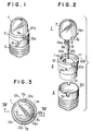
- a light emission diode lamp unit 1 a spacer 2 and an Edison type lamp cap 3 are preliminarily individually produced.
- the lamp unit 1 is produced such that light emission diode elements 5 are attached onto corresponding lead-substrates 4a of a lead-conductor 4 and connected with each other by lead wires 6, and then the light emission diode elements 5, the lead-conductor 4 and the lead wires 6 are integrally embedded in a molding of a light transmissible resin material 7 with only the respective ends of lead-strip portions 4b exposed outside.
- Reference numeral 8 designates a current limiting element which is a resistor or a capacitor suitable for the working voltage and current to enable the light emission diode elements 5 to be actuated to illuminate through this current limiting element 8.
- protrusions 7a and 7a are integrally formed in the light transmissible molding 7 at its lower end portion such that the protrusions 7a and 7a can respectively engage with axially formed grooves 12a and 12a of the spacer 2 which will be described later more in detail.
- the lead-conductor 4 is bent at a right angle at its upper end portion to form the above-mentioned lead-substrate portions 4a extending in the radial direction of the above-mentioned spacer 2.
- the above-mentioned lead-strip portions 4b extending in the axial direction of the spacer 2 are formed at the lower portion of the lead-conductor 4 and previously connected to each other through connecting portions 4c of the lead-conductor 4.
- each of the unit blocks includes five digitally divided lead-strip portions 4b and the lead-substrate portions 4a which are previously shaped so that the light emission diode elements 5 may be properly attached thereto.
- two of the lead-strip portions 4b of each block are formed as a pair of connecting terminals 4b l and 4b 2 .
- each unit block namely each lead-conductor 4
- the light emission diode elements 5 are attached onto the lead-substrate portions 4a and the attached light emission diode elements 5 are previously connected.
- each unit block or lead-conductor 4 including the lead-substrate portions 4a, the light emission diode elements 5 and the lead-strip portions 4b are embedded in the light transmissive resin molding 7 with the respective ends of the lead-strip portions 4b exposed outside the molding 7.
- the respective unit blocks are separated into individual lead-conductors 4 by properly cutting off unnecessary parts of the connecting portions 4c.
- B l' B 2' B 3 indicated by two-dotted line are the unnecessary parts of the connecting portions 4c to be selectively cut off. That is, for example, in the case where four light emission diode elements 5 are used to constitute such a series-connected circuit as shown in Fig.
- the connecting portions 4c are cut off at the parts A 1 , A 2 and A3 and connections are previously made at the lead-substrate portions 4a.
- the connecting portions 4c are cut off at the parts B1, B 2 and B 3 and necessary connection is made predeterminedly at the lead-substrate portions 4a as shown in Fig. 11.
- each unit block is arranged to have five lead-strip portions 4b, it is of course that the present invention is not limited to this number of the lead-strip portions 4b and at least two lead-strip portions may be sufficient to constitute each unit block and that the number of the light emission diode elements to be attached to the lead-substrate may be selected in accordance with the demand.
- the spacer 2 of an insulator material has a substantially cylindrical external form, and a support portion 11 on which the lamp unit 1 may be mounted is formed at the upper opening portion of the spacer 2.
- a through hole lla is formed at the center of the support portion 11 so that the respective forward ends of the lead-strip portions 4b and the connecting terminals 4b 1 , 4b 2 extending downward from the lower end of the lamp unit 1 and the resistor 8 can be passed therethrough.
- a circumferential wall 12 is uprightly formed around the support portion 11 and longitudinal grooves or slots 12a, 12a and 12b are formed at three portions of the circumferential wall 12.
- a guide groove or slot llb continued to the longitudinal groove or slot 12b is formed in the circumferential wall 12 at a portion under the opening plane of the support portion 11 so that the connecting terminal 4b 1 may be led into this guide groove or slot llb when the lamp unit 1 is attached to the spacer 2.
- a pair of protrusions 12c and 12c downward extending from the lower end of the circumferential wall 12 are formed in opposition to each other, so that uneven engagement can be made between these protrusions 12c and 12c and grooves or slots 31 and 31 formed at the upper opening portion of the lamp cap 3.
- the lamp cap 3 a one available on the market is usually used after it has been somewhat worked.
- an Edison type lamp cap is used and three grooves or slots 31, 31 and 32 are formed in the lamp cap at its upper opening end portion.
- the two grooves or slots 31 and 31. is formed in opposition to each other so that they are used for the uneven engagement with the protrusions 12c and 12c of the spacer 2 as described above.
- the other groove or slot 32 is formed corresponding to the led-out portion of the connecting terminal 4b1.
- Reference numeral 33 designates a contact formed at a lower end portion of the lamp cap 3 and insulated from the lamp cap 3 with an insulating material 34.
- an upper lead wire 8a of the current limiting element 8 is inserted into and passed through a through hole a formed in the connecting terminal 4b 2 extending downward from the lower end of the lamp unit 1 and soldered thereat.
- the lamp unit 1 with the current limiting element 8 soldered thereto is put on the spacer 2 at its upper opening side so that the protrusions 7a and 7a engage with the respective longitudinal grooves or slots 12a and 12a to fixedly attach the lamp unit 1 to the spacer 2.
- the lower lead wire 8b of the current limiting element 8 is exposed at the lower side of the spacer 2.
- the protrusions 12a and 12a of the spacer 2 are engaged with the grooves or slots 31 and 31 of the lamp cap 3 to attach the lamp cap 3 to the assembly of the lamp unit 1 and the spacer 2 such that the lead wire 8b of the current limiting element 8 is passed through a through hole 33a formed in the contact 33 at its center.
- the connecting terminal 4b l is led in the groove or slot 32 of the lamp cap 3.
- soldering is applied to the gap Kl between the connecting terminal 4b l and the lamp cap 3 and the gap K2 between the lead wire 8b and the contact 33 to thereby ensure the electrical and mechanical connection therebetween to complete the assembling of the light emission diode lamp.
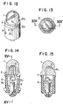
- Figs. 12 to 15 illustrate another embodiment of the light emission diode lamp according to the present invention. This embodiment is substantially the same as the first embodiment excepting that a swan type lamp cap 9 is used in this embodiment.
- the same component as that used in the first embodiment is represented by the same reference numeral or symbol and the description about the procedure of assembling is omitted here because it is quite the same as in the first embodiment.
- the lamp cap is not always limited to such an Edison type or such a swan type, according to the present invention, but any type lamp cap, such as for an aircraft, available on the market can of course be used.
- the standardized dimension of the upper opening portion of the swan type lamp cap 9 is normally different from that of the Edison type lamp cap 3.
- the inside diameter of the upper opening portions of the spacer 2 engaged with the swan type lamp cap 9 and that of the spacer.2 engaged with the Edison type lamp cap 3 can be worked as the same dimension and the outside diameters of the lower opening portions of these spacers 2 are worked as the different dimensions in order to engage with the swan type and the Edison type lamp caps 3, 9 respectively.
- the present invention is advantageous in that the mass production of light emission diode lamps of this type is enabled so as to improve the efficiency in production to provide inexpensive light emission diode lamps.
- the lamp unit 1, the spacer 2 and the lamp cap 3 or 9 are arranged such that they are readily attached with each other through uneven engagement so that a light emission diode lamp having such a stable performance that there is little possibility of occurrence of disconnection at the soldered portions or ricketiness between the lamp unit 1 and the lamp cap 3 or 9 even in the case an external force such as vibrations, shocks, rotational forces, etc. is applied to the lamp.
Abstract
Description
- The present invention relates to a lamp using a light emission diode (hereinafter referred to as a light emission diode lamp) and a method of producing it.
- When comparison is made between a light emission diode lamp and a small-sized incandescent lamp as an illumination source, it is known well that the former is superior to the latter in life, reliability, consumed power, etc. Recently, such an advantageous light emission diode lamp is being developed. However, there is a problem in the interchangeability between such a light emission diode lamp and the conventional incandescent lamp in practical use. As an solution of this problem, a so- called lamp-cap type light emission diode lamp, which comprises a light emission diode as an illumination source and a lamp cap similar to that of an incandescent lamp as a terminal member to be connected to a power source, has been used.
- An object of the present invention is to provide a light emission diode lamp and a method for producing thereof in which the connection between a lead-conductor of a light emission diode and a lamp cap can be easily performed so as to be preferable for the mass production of such a light emission diode lamp.
- Another object of the present invention is to provide a light emission diode lamp and a method for producing thereof in which the light emission diode lamp has a stable characteristic such that disconnection and/or ricketiness is prevented from occurring even when an external force such as vibrations, shocks, rotational force, or the like, is applied to the light emission diode lamp.
- The above and other objects, features and advantages of the present invention will be apparent from the following detailed description of preferred embodiments thereof taken in conjunction with the accompanying drawings, in which:
- Fig. 1 is a perspective view of an embodiment of the light emission diode lamp according to the present invention;
- Fig. 2 is an exploded perspective view of the embodiment of Fig. 1;
- Fig. 3 is a plan view of the embodiment of Fig. 1;
- Fig. 4 is a longitudinal front view partly in section along IV-IV line in Fig. 3;
- Fig. 5 is a longitudinal side view partly in section along V-V line in Fig. 4;
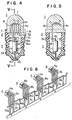
- Fig. 6 is a perspective view of the conductor for explaining the process of producing the light emission diode lamp according to the present invention;
- Fig. 7 is a front view of the lead-conductor shown in Fig. 6;
- Fig. 8 is a circuit diagram of a light emission diode lamp in which light emission diodes are connected in series with each other;
- Fig. 9 is a plan view of the lead-substrate portion showing an actually wired state of the circuit as shown in Fig. 8;
- Fig. 10 is a circuit diagram of a light emission diode lamp in which light emission diodes are connected in series-parallel with each other;
- Fig. 11 is a plan view of the lead-substrate portion showing an actually wired state of the circuit as shown in Fig. 10;
- Fig. 12 is a perspective view of another embodi- ment of the light emission diode lamp according to the present invention;
- Fig. 13 is a plan view of the embodiment of Fig. 12;
- Fig. 14 is a longitudinal front view partly in section along XIV-XIV line in Fig. 13; and
- Fig. 15 is a longitudinal side view partly in section along XV-XV line in Fig. 14.
- Referring to the drawings, preferred embodiments of the present invention will be described hereunder.
- Figs. 1 to 11 show an embodiment of the present invention. In producing the light emission diode lamp according to the present invention, a light emission
diode lamp unit 1, aspacer 2 and an Edisontype lamp cap 3 are preliminarily individually produced. Thelamp unit 1 is produced such that lightemission diode elements 5 are attached onto corresponding lead-substrates 4a of a lead-conductor 4 and connected with each other by lead wires 6, and then the lightemission diode elements 5, the lead-conductor 4 and the lead wires 6 are integrally embedded in a molding of a lighttransmissible resin material 7 with only the respective ends of lead-strip portions 4b exposed outside. -
Reference numeral 8 designates a current limiting element which is a resistor or a capacitor suitable for the working voltage and current to enable the lightemission diode elements 5 to be actuated to illuminate through this current limitingelement 8. - According to the present invention,
protrusions transmissible molding 7 at its lower end portion such that theprotrusions grooves spacer 2 which will be described later more in detail. - The lead-
conductor 4 is bent at a right angle at its upper end portion to form the above-mentioned lead-substrate portions 4a extending in the radial direction of the above-mentionedspacer 2. The above-mentioned lead-strip portions 4b extending in the axial direction of thespacer 2 are formed at the lower portion of the lead-conductor 4 and previously connected to each other through connectingportions 4c of the lead-conductor 4. - Referring to Figs. 6 and 7, a series of continued unit blocks each for the lead-
conductor 4 is punched out of a conductive sheet by using a press. The respective unit blocks are connected through the connectingportions 4c and each of the unit blocks includes five digitally divided lead-strip portions 4b and the lead-substrate portions 4a which are previously shaped so that the lightemission diode elements 5 may be properly attached thereto. In this embodiment, two of the lead-strip portions 4b of each block are formed as a pair of connectingterminals portions 4c is used to form the connectingterminal 4b1 which is to be connected to the Edisontype lamp cap 3, while one of the lead-strip portions 4b2 is downward extended and the extended end portion is rectangularly shaped to form theconnecting terminal 4b to which theresistor 8 is to be connected. As to each unit block, namely each lead-conductor 4, the lightemission diode elements 5 are attached onto the lead-substrate portions 4a and the attached lightemission diode elements 5 are previously connected. Then each unit block or lead-conductor 4 including the lead-substrate portions 4a, the lightemission diode elements 5 and the lead-strip portions 4b are embedded in the lighttransmissive resin molding 7 with the respective ends of the lead-strip portions 4b exposed outside themolding 7. Thereafter, the respective unit blocks are separated into individual lead-conductors 4 by properly cutting off unnecessary parts of the connectingportions 4c. In Fig. 7 the portions A1, A2, A3. Bl' B2' B3 indicated by two-dotted line are the unnecessary parts of the connectingportions 4c to be selectively cut off. That is, for example, in the case where four lightemission diode elements 5 are used to constitute such a series-connected circuit as shown in Fig. 8, the connectingportions 4c are cut off at the parts A1, A2 and A3 and connections are previously made at the lead-substrate portions 4a. On the other hand, in the case where each pair of the lightemission diode elements 5 are connected in series to each other and the thus series-connected two pairs are connected in parallel with each other as shown in Fig. 10, the connectingportions 4c are cut off at the parts B1, B2 and B3 and necessary connection is made predeterminedly at the lead-substrate portions 4a as shown in Fig. 11. - Although in the embodiment, each unit block is arranged to have five lead-
strip portions 4b, it is of course that the present invention is not limited to this number of the lead-strip portions 4b and at least two lead-strip portions may be sufficient to constitute each unit block and that the number of the light emission diode elements to be attached to the lead-substrate may be selected in accordance with the demand. - The
spacer 2 of an insulator material has a substantially cylindrical external form, and a support portion 11 on which thelamp unit 1 may be mounted is formed at the upper opening portion of thespacer 2. A through hole lla is formed at the center of the support portion 11 so that the respective forward ends of the lead-strip portions 4b and the connectingterminals lamp unit 1 and theresistor 8 can be passed therethrough. Acircumferential wall 12 is uprightly formed around the support portion 11 and longitudinal grooves orslots circumferential wall 12. Two of these three longitudinal grooves orslots protrusions slots slot 12b is formed in thecircumferential wall 12 at a portion under the opening plane of the support portion 11 so that the connectingterminal 4b1 may be led into this guide groove or slot llb when thelamp unit 1 is attached to thespacer 2. Further, in thespacer 2, a pair ofprotrusions circumferential wall 12 are formed in opposition to each other, so that uneven engagement can be made between theseprotrusions slots lamp cap 3. As thelamp cap 3, a one available on the market is usually used after it has been somewhat worked. In this embodiment, an Edison type lamp cap is used and three grooves orslots slots protrusions spacer 2 as described above. The other groove orslot 32 is formed corresponding to the led-out portion of the connecting terminal 4b1.Reference numeral 33 designates a contact formed at a lower end portion of thelamp cap 3 and insulated from thelamp cap 3 with aninsulating material 34. - In assembling the thus prepared components to constitute a light emission diode lamp, an
upper lead wire 8a of the current limitingelement 8 is inserted into and passed through a through hole a formed in the connectingterminal 4b2 extending downward from the lower end of thelamp unit 1 and soldered thereat. Thelamp unit 1 with the current limitingelement 8 soldered thereto is put on thespacer 2 at its upper opening side so that theprotrusions slots lamp unit 1 to thespacer 2. In the present state, thelower lead wire 8b of the current limitingelement 8 is exposed at the lower side of thespacer 2. Next, theprotrusions spacer 2 are engaged with the grooves orslots lamp cap 3 to attach thelamp cap 3 to the assembly of thelamp unit 1 and thespacer 2 such that thelead wire 8b of the current limitingelement 8 is passed through a through hole 33a formed in thecontact 33 at its center. At this time, theconnecting terminal 4bl is led in the groove orslot 32 of thelamp cap 3. Finally, soldering is applied to the gap Kl between the connectingterminal 4bl and thelamp cap 3 and the gap K2 between thelead wire 8b and thecontact 33 to thereby ensure the electrical and mechanical connection therebetween to complete the assembling of the light emission diode lamp. - Figs. 12 to 15 illustrate another embodiment of the light emission diode lamp according to the present invention. This embodiment is substantially the same as the first embodiment excepting that a swan
type lamp cap 9 is used in this embodiment. In Figs. 12 to 15, the same component as that used in the first embodiment is represented by the same reference numeral or symbol and the description about the procedure of assembling is omitted here because it is quite the same as in the first embodiment. - The lamp cap is not always limited to such an Edison type or such a swan type, according to the present invention, but any type lamp cap, such as for an aircraft, available on the market can of course be used.
- In addition, the standardized dimension of the upper opening portion of the swan
type lamp cap 9 is normally different from that of the Edisontype lamp cap 3. However, the inside diameter of the upper opening portions of thespacer 2 engaged with the swantype lamp cap 9 and that of the spacer.2 engaged with the Edisontype lamp cap 3 can be worked as the same dimension and the outside diameters of the lower opening portions of thesespacers 2 are worked as the different dimensions in order to engage with the swan type and the Edison type lamp caps 3, 9 respectively. - As described above, according to the present invention, assembling is performed such that the
lamp unit 1 is attached to thelamp cap spacer 2 after thelamp unit 1 has been first attached to thespacer 2 so that the pair of lead-strip portions led out from the lead-substrate, the lamp cap, and the contact formed at the bottom portion of the lamp cap can be put in place in the processes successively assembling the components, resulting in facilitation of electrical connection. Thus, the present invention is advantageous in that the mass production of light emission diode lamps of this type is enabled so as to improve the efficiency in production to provide inexpensive light emission diode lamps. Further, thelamp unit 1, thespacer 2 and thelamp cap lamp unit 1 and thelamp cap
Claims (13)
Applications Claiming Priority (2)
| Application Number | Priority Date | Filing Date | Title |
|---|---|---|---|
| JP185871/82 | 1982-10-21 | ||
| JP57185871A JPS5974687A (en) | 1982-10-21 | 1982-10-21 | Light emitting diode lamp |
Publications (2)
| Publication Number | Publication Date |
|---|---|
| EP0107480A2 true EP0107480A2 (en) | 1984-05-02 |
| EP0107480A3 EP0107480A3 (en) | 1986-07-16 |
Family
ID=16178332
Family Applications (1)
| Application Number | Title | Priority Date | Filing Date |
|---|---|---|---|
| EP83306361A Withdrawn EP0107480A3 (en) | 1982-10-21 | 1983-10-19 | Light emission diode lamp and method of producing it |
Country Status (2)
| Country | Link |
|---|---|
| EP (1) | EP0107480A3 (en) |
| JP (1) | JPS5974687A (en) |
Cited By (19)
| Publication number | Priority date | Publication date | Assignee | Title |
|---|---|---|---|---|
| FR2576719A1 (en) * | 1985-01-25 | 1986-08-01 | Jaeger | Connector support for a light-emitting diode and motor-vehicle dashboard using this support |
| EP0315905A2 (en) * | 1987-11-07 | 1989-05-17 | Werner Müller | Electroluminescent device |
| EP0400193A1 (en) * | 1989-06-02 | 1990-12-05 | Siemens Aktiengesellschaft | Sensing device |
| DE9202608U1 (en) * | 1992-02-28 | 1992-09-17 | Ebt Licht-Technik Gmbh, 6702 Bad Duerkheim, De | |
| DE4141979A1 (en) * | 1991-12-19 | 1993-06-24 | Sel Alcatel Ag | High power light-emitting diode with hermetically sealed casing - has internal flange acting as bayonet coupling locking diode in seating provided by illuminated block |
| DE4141978A1 (en) * | 1991-12-19 | 1993-06-24 | Sel Alcatel Ag | High power light-emitting diode with hermetically-sealed casing - has threaded outer surface allowing direct fitting of diode into threaded socket in transparent or translucent block |
| DE4141980A1 (en) * | 1991-12-19 | 1993-07-01 | Sel Alcatel Ag | High power light emitting diode e.g. for replacing incandescent lamp - has active diode moulded into transparent body together with connections to outer contact points |
| EP1117135A2 (en) * | 2000-01-12 | 2001-07-18 | Oxley Developments Company Limited | Led package |
| WO2002041406A1 (en) * | 2000-11-16 | 2002-05-23 | Emcore Corporation | Microelectronic package having improved light extraction |
| WO2002103794A1 (en) * | 2001-06-15 | 2002-12-27 | Lednium Pty Limited | A method of producing a lamp |
| US6809475B2 (en) | 2000-06-15 | 2004-10-26 | Lednium Pty Limited | Led lamp with light-emitting junctions arranged in a three-dimensional array |
| EP1793158A2 (en) * | 2005-11-08 | 2007-06-06 | United Technologies Corporation | Led Replacement bulb |
| US7320632B2 (en) | 2000-06-15 | 2008-01-22 | Lednium Pty Limited | Method of producing a lamp |
| US7704762B2 (en) | 2002-06-14 | 2010-04-27 | Lednium Technology Pty Limited | Lamp and method of producing a lamp |
| WO2010088003A1 (en) * | 2009-02-02 | 2010-08-05 | Teledyne Lighting And Display Products, Inc. | Efficient illumination device for aircraft |
| CN102157505A (en) * | 2011-01-20 | 2011-08-17 | 日月光半导体制造股份有限公司 | Light-emitting module |
| CN102439350A (en) * | 2009-05-12 | 2012-05-02 | 马雷蒂控股有限公司 | Led lamp system |
| US8415895B2 (en) | 2006-12-15 | 2013-04-09 | Osram Gesellschaft Mit Beschrankter Haftung | Lamp comprising a base and at least one light-emitting semiconductor component |
| US8534901B2 (en) | 2010-09-13 | 2013-09-17 | Teledyne Reynolds, Inc. | Collimating waveguide apparatus and method |
Families Citing this family (3)
| Publication number | Priority date | Publication date | Assignee | Title |
|---|---|---|---|---|
| JPH02156904A (en) * | 1988-12-08 | 1990-06-15 | Tobishima Corp | Shoes box |
| JP2014038989A (en) * | 2012-08-20 | 2014-02-27 | Toshiba Corp | Semiconductor light-emitting device and lighting device |
| JP5985341B2 (en) * | 2012-10-03 | 2016-09-06 | シャープ株式会社 | Manufacturing method of conductive frame and light source substrate |
Citations (7)
| Publication number | Priority date | Publication date | Assignee | Title |
|---|---|---|---|---|
| US3609475A (en) * | 1970-05-04 | 1971-09-28 | Hewlett Packard Co | Light-emitting diode package with dual-colored plastic encapsulation |
| DE2315709A1 (en) * | 1973-03-29 | 1974-10-10 | Licentia Gmbh | RADIATION-EMISSING SEMI-CONDUCTOR ARRANGEMENT WITH HIGH RADIATION POWER |
| US3875456A (en) * | 1972-04-04 | 1975-04-01 | Hitachi Ltd | Multi-color semiconductor lamp |
| FR2330105A1 (en) * | 1975-10-31 | 1977-05-27 | Western Electric Co | LIGHT EMISSION DISPLAY DEVICE |
| DE2818973A1 (en) * | 1978-04-28 | 1979-11-08 | Siemens Ag | Long life miniature warning lamp - uses LED and special resistance under transparent cover for reduced output in sunlight |
| FR2495278A3 (en) * | 1980-11-28 | 1982-06-04 | Alsthom Cgee | LED signalling or warning light for control panel - has three LED's mounted on base plate attached to conventional lamp base and selectively connected to base contacts |
| GB2098714A (en) * | 1980-06-04 | 1982-11-24 | Tranilamp Ltd | LED cluster assembly |
-
1982
- 1982-10-21 JP JP57185871A patent/JPS5974687A/en active Granted
-
1983
- 1983-10-19 EP EP83306361A patent/EP0107480A3/en not_active Withdrawn
Patent Citations (7)
| Publication number | Priority date | Publication date | Assignee | Title |
|---|---|---|---|---|
| US3609475A (en) * | 1970-05-04 | 1971-09-28 | Hewlett Packard Co | Light-emitting diode package with dual-colored plastic encapsulation |
| US3875456A (en) * | 1972-04-04 | 1975-04-01 | Hitachi Ltd | Multi-color semiconductor lamp |
| DE2315709A1 (en) * | 1973-03-29 | 1974-10-10 | Licentia Gmbh | RADIATION-EMISSING SEMI-CONDUCTOR ARRANGEMENT WITH HIGH RADIATION POWER |
| FR2330105A1 (en) * | 1975-10-31 | 1977-05-27 | Western Electric Co | LIGHT EMISSION DISPLAY DEVICE |
| DE2818973A1 (en) * | 1978-04-28 | 1979-11-08 | Siemens Ag | Long life miniature warning lamp - uses LED and special resistance under transparent cover for reduced output in sunlight |
| GB2098714A (en) * | 1980-06-04 | 1982-11-24 | Tranilamp Ltd | LED cluster assembly |
| FR2495278A3 (en) * | 1980-11-28 | 1982-06-04 | Alsthom Cgee | LED signalling or warning light for control panel - has three LED's mounted on base plate attached to conventional lamp base and selectively connected to base contacts |
Non-Patent Citations (1)
| Title |
|---|
| RESEARCH DISCLOSURE, no. 191, March 1980, pages 105-106, 19107, Vaut. Hauts, GB; R.F. McKEEVER: "LED flashlight" * |
Cited By (26)
| Publication number | Priority date | Publication date | Assignee | Title |
|---|---|---|---|---|
| FR2576719A1 (en) * | 1985-01-25 | 1986-08-01 | Jaeger | Connector support for a light-emitting diode and motor-vehicle dashboard using this support |
| EP0315905A2 (en) * | 1987-11-07 | 1989-05-17 | Werner Müller | Electroluminescent device |
| EP0315905A3 (en) * | 1987-11-07 | 1990-05-02 | Werner Müller | Electroluminescent device |
| EP0400193A1 (en) * | 1989-06-02 | 1990-12-05 | Siemens Aktiengesellschaft | Sensing device |
| DE4141979A1 (en) * | 1991-12-19 | 1993-06-24 | Sel Alcatel Ag | High power light-emitting diode with hermetically sealed casing - has internal flange acting as bayonet coupling locking diode in seating provided by illuminated block |
| DE4141978A1 (en) * | 1991-12-19 | 1993-06-24 | Sel Alcatel Ag | High power light-emitting diode with hermetically-sealed casing - has threaded outer surface allowing direct fitting of diode into threaded socket in transparent or translucent block |
| DE4141980A1 (en) * | 1991-12-19 | 1993-07-01 | Sel Alcatel Ag | High power light emitting diode e.g. for replacing incandescent lamp - has active diode moulded into transparent body together with connections to outer contact points |
| DE9202608U1 (en) * | 1992-02-28 | 1992-09-17 | Ebt Licht-Technik Gmbh, 6702 Bad Duerkheim, De | |
| US5349509A (en) * | 1992-02-28 | 1994-09-20 | Ebt Licht-Technik Gmbh | Indicator element |
| EP1117135A2 (en) * | 2000-01-12 | 2001-07-18 | Oxley Developments Company Limited | Led package |
| EP1117135A3 (en) * | 2000-01-12 | 2007-03-21 | Oxley Developments Company Limited | Led package |
| US6809475B2 (en) | 2000-06-15 | 2004-10-26 | Lednium Pty Limited | Led lamp with light-emitting junctions arranged in a three-dimensional array |
| US7320632B2 (en) | 2000-06-15 | 2008-01-22 | Lednium Pty Limited | Method of producing a lamp |
| US7352127B2 (en) | 2000-06-15 | 2008-04-01 | Lednium Pty Limited | LED lamp with light-emitting junction arranged in three-dimensional array |
| US7023022B2 (en) | 2000-11-16 | 2006-04-04 | Emcore Corporation | Microelectronic package having improved light extraction |
| WO2002041406A1 (en) * | 2000-11-16 | 2002-05-23 | Emcore Corporation | Microelectronic package having improved light extraction |
| WO2002103794A1 (en) * | 2001-06-15 | 2002-12-27 | Lednium Pty Limited | A method of producing a lamp |
| US7704762B2 (en) | 2002-06-14 | 2010-04-27 | Lednium Technology Pty Limited | Lamp and method of producing a lamp |
| EP1793158A3 (en) * | 2005-11-08 | 2008-06-25 | United Technologies Corporation | Led Replacement bulb |
| EP1793158A2 (en) * | 2005-11-08 | 2007-06-06 | United Technologies Corporation | Led Replacement bulb |
| US8415895B2 (en) | 2006-12-15 | 2013-04-09 | Osram Gesellschaft Mit Beschrankter Haftung | Lamp comprising a base and at least one light-emitting semiconductor component |
| WO2010088003A1 (en) * | 2009-02-02 | 2010-08-05 | Teledyne Lighting And Display Products, Inc. | Efficient illumination device for aircraft |
| US8083384B2 (en) | 2009-02-02 | 2011-12-27 | Teledyne Technologies Incorporated | Efficient illumination device for aircraft |
| CN102439350A (en) * | 2009-05-12 | 2012-05-02 | 马雷蒂控股有限公司 | Led lamp system |
| US8534901B2 (en) | 2010-09-13 | 2013-09-17 | Teledyne Reynolds, Inc. | Collimating waveguide apparatus and method |
| CN102157505A (en) * | 2011-01-20 | 2011-08-17 | 日月光半导体制造股份有限公司 | Light-emitting module |
Also Published As
| Publication number | Publication date |
|---|---|
| JPS5974687A (en) | 1984-04-27 |
| JPS6329433B2 (en) | 1988-06-14 |
| EP0107480A3 (en) | 1986-07-16 |
Similar Documents
| Publication | Publication Date | Title |
|---|---|---|
| EP0107480A2 (en) | Light emission diode lamp and method of producing it | |
| EP0078037B1 (en) | Light emission diode lamp and method for producing thereof | |
| US5860830A (en) | Lamp socket structure | |
| US3783437A (en) | Lamp and socket for decorative string set | |
| EP0151806A2 (en) | Electric lamp with insulating base | |
| US4727648A (en) | Circuit component mount and assembly | |
| JP3604401B2 (en) | Lighting elements for lighting function symbols or signaling functions | |
| US4857877A (en) | Transformer having coaxial coils | |
| EP0588670A1 (en) | Lamp with integrated electronic module | |
| US7207847B2 (en) | Vehicle interior illumination lamp | |
| US4752710A (en) | Electric lamp with insulating base providing improved wire retention | |
| US6074244A (en) | Stringer of decorative lights | |
| US4991071A (en) | Light string set | |
| US6932639B2 (en) | Electroluminescent cable connector | |
| EP0748516B1 (en) | Electric lamp | |
| CA1173922A (en) | Wedge base lamp socket assembly | |
| US5951152A (en) | Light source housing apparatus and method of manufacture | |
| US5148086A (en) | Means for securing insulation displacement terminals to leads extending from a fluorescent light ballast | |
| KR100521236B1 (en) | Compact low-pressure discharge lamp | |
| US6048220A (en) | Lampholder connector for multiple fluorescent lamps | |
| KR100602391B1 (en) | Compact low pressure discharge lamp | |
| JP3042736B2 (en) | Multi-pole connector | |
| CN110858697A (en) | Method for assembling electric connector for printed circuit board | |
| US5742218A (en) | Flyback transformer | |
| US6642660B1 (en) | Filament shunt member for decorative lamp |
Legal Events
| Date | Code | Title | Description |
|---|---|---|---|
| PUAI | Public reference made under article 153(3) epc to a published international application that has entered the european phase |
Free format text: ORIGINAL CODE: 0009012 |
|
| AK | Designated contracting states |
Designated state(s): DE FR GB IT |
|
| PUAL | Search report despatched |
Free format text: ORIGINAL CODE: 0009013 |
|
| AK | Designated contracting states |
Kind code of ref document: A3 Designated state(s): DE FR GB IT |
|
| 17P | Request for examination filed |
Effective date: 19861215 |
|
| 17Q | First examination report despatched |
Effective date: 19880610 |
|
| STAA | Information on the status of an ep patent application or granted ep patent |
Free format text: STATUS: THE APPLICATION IS DEEMED TO BE WITHDRAWN |
|
| 18D | Application deemed to be withdrawn |
Effective date: 19881021 |
|
| RIN1 | Information on inventor provided before grant (corrected) |
Inventor name: KIMURA, HARUO Inventor name: FUJITA, TEIZO |