EP0110060A1 - FET voltage level shift circuitry - Google Patents
FET voltage level shift circuitry Download PDFInfo
- Publication number
- EP0110060A1 EP0110060A1 EP83109944A EP83109944A EP0110060A1 EP 0110060 A1 EP0110060 A1 EP 0110060A1 EP 83109944 A EP83109944 A EP 83109944A EP 83109944 A EP83109944 A EP 83109944A EP 0110060 A1 EP0110060 A1 EP 0110060A1
- Authority
- EP
- European Patent Office
- Prior art keywords
- csi
- nodes
- latch
- voltage
- signals
- Prior art date
- Legal status (The legal status is an assumption and is not a legal conclusion. Google has not performed a legal analysis and makes no representation as to the accuracy of the status listed.)
- Granted
Links
Images

Classifications
-
- H—ELECTRICITY
- H03—ELECTRONIC CIRCUITRY
- H03K—PULSE TECHNIQUE
- H03K19/00—Logic circuits, i.e. having at least two inputs acting on one output; Inverting circuits
- H03K19/0175—Coupling arrangements; Interface arrangements
- H03K19/0185—Coupling arrangements; Interface arrangements using field effect transistors only
- H03K19/018507—Interface arrangements
- H03K19/01855—Interface arrangements synchronous, i.e. using clock signals
-
- H—ELECTRICITY
- H03—ELECTRONIC CIRCUITRY
- H03K—PULSE TECHNIQUE
- H03K3/00—Circuits for generating electric pulses; Monostable, bistable or multistable circuits
- H03K3/02—Generators characterised by the type of circuit or by the means used for producing pulses
- H03K3/353—Generators characterised by the type of circuit or by the means used for producing pulses by the use, as active elements, of field-effect transistors with internal or external positive feedback
- H03K3/356—Bistable circuits
- H03K3/356104—Bistable circuits using complementary field-effect transistors
Definitions
- the invention relates to FET voltage level shift circuitry and is more particularly, but not exclusively concerned with circuits for converting TTL logic signal levels to MOS logic signal levels.
- MOS semiconductor art large scale integrated circuits are produced. Included among this class of semiconductor devices are MOS memories which are addressed through a plurality of address signals and the logical complement of these signals.
- TTL circuitry operates at different voltage levels providing a binary 1 at greater than 2.2 volts and a binary 0 at less than .6 volts. These logic levels are insufficient and in some instances incompatible with MOS logic levels.
- Buffer circuits have been devised to provide conversion of TTL logic levels to levels compatible with MOS logic circuits. These are included in a 16K dynamic RAM, No. MK 4116, manufactured by MOSTEK which can be driven directly with TTL logic. The device is power efficient but requires three clocks to operate. The multiple clocks impose an undesirable speed limitation on the operation of the buffer and hence to the remaining circuitry connected with the buffer. ,
- a cross coupled latch is provided which is controlled by chip enable signals CSI, and its complement CSI.
- the latch is disabled conserving power, and the cross coupled latch receives as an input a reference level and a TTL logic level.
- the latch will assume a state corresponding to the received TTL level during a second state of the signals.
- a pass circuit connects the latch nodes to first and second inverter chains.
- the latch assumes the appropriate logic state defined by the reference level and TTL level and the pass circuit makes the connection between inverter chains and the nodes providing a MOS logical level and its complement.
- the cross-coupled latch is isolated from the inverter chains by an interrupt function of the pass circuit.
- the invention provides FET circuitry for converting a first signal represented by the potential difference between a reference voltage and a first logic voltage at one or other of two first voltage levels to a second signal represented by the potential difference between a second reference voltage and a second logic voltage at one or other of two second voltage levels, said circuitry comprising a cross-coupled bistable input circuit having two inputs to which the voltages of the first signal are applied and two output nodes at which complementary output voltages are manifested; first and second output circuits each comprising at least one voltage transition stage including two complementary FET's having their controlled current paths in series and their gates connected to control terminals, connected in parallel between supply lines to which the second voltage levels are applied; two circuit-paths respectively connecting the two output nodes to the gate control terminals, said circuit-paths including the controlled current paths of at least two isolating transistors of which the gates are respectively connected to terminals to which complementary valued, binary input timing signals are supplied in use to render the isolating transistor conductive for timed intervals; and two voltage-clam
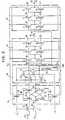
- FIG. 1 there is shown an MOS RAM 11 having a plurality of address inputs Ao through An.
- the address lines also include complementary inputs Ao to A n.
- the MOS RAM 11 is addressed by a TTL logic circuit 5.
- the input TTL logic levels are less than .6 volts and greater than 2.2 volts corresponding to a binary 0 and 1 respectively.
- the output logic levels are between 0 and 5 volts respectively for driving the address inputs of MOS RAM 11.
- the buffer 7 requires a single clock represented by CSI and its complement, CSI.
- the elements of the buffer are field effect transistors of either N or P channel type hereinafter referred to as an NFET or PFET.
- the input cross coupled latch is provided by circuitry 15.
- the cross coupled latch 15 includes first and second switches comprising NFET 34 and PFET 28. The switches feed a pair of parallel connected, serial transistor pairs 25, 30 and 26, 32. FET 25 and 26 are P channel and 30 and 32 are N channel. The gates of each transistor pair 25, 30 and 26, 32 are connected together with the junction of an opposite transistor pair to form first and second Nodes N 1 , N 2 .
- the cross coupled latch 15 receives on each node N 1 , N 2 a reference voltage and TTL logic level through NFET 22 and NFET 23.
- the chip select, CSI occurs when the MOSRAM 11 address lines are to be addressed.
- the CSI pulse along with its complement CSI is the only clock pulse required to operate the buffer.
- the nodes of the cross coupled latch 15 are connected to a current path circuit 16.
- the current path circuit 16 also operates under control of CSI and CSI.
- NFET 39, 43 and PFET 38, 41 are gated off thus isolating the inverter chains 18 and 19 from Nodes N 1 , N 2 of the cross coupled latch 15, and NFET 45 and 47 are gated on returning the inverter chains 18, 19 inputs, N 3 , N 4 to ground.
- the inverter chains are identical except for their input connections.
- the chains comprise three PFETS 49, 52, 54 and 56, 58, 60 having a drain connection to VDD, and serially connected to three NFETS, 50, 53, 55, and 57, 59, 61 which provide through respective source connections a return connection to ground.
- the gates of a pair of serially connected transistors are connected together to form an input connection, and the common connections of the NFET and PFET form an output connection.
- the entire circuit functions to minimize power consumption and maximize speed using only a single clock pulse CSI and its complement.
- the switches in the latch 15 comprising NFET 34 and PFET 28 are activated and latch 15 assumes the state determined by TTL logic level Ao.
- Inverter chains 18 and 19 are connected to the nodes N 1 and N2 and provide complementary MOS output levels Ao and Ao.
- the buffer of Figure 2 can be implemented in CMOS. The following description of each of the FETS of Figure 2 can be implemented to yield one embodiment of the invention.
- the foreging circuit provides a low power high speed address buffer for converting TTL level signals to MOS level signals and their complement.
Abstract
Description
- The invention relates to FET voltage level shift circuitry and is more particularly, but not exclusively concerned with circuits for converting TTL logic signal levels to MOS logic signal levels. In the MOS semiconductor art large scale integrated circuits are produced. Included among this class of semiconductor devices are MOS memories which are addressed through a plurality of address signals and the logical complement of these signals.
- In many applications of memories and other types of circuit devices produced in the technology it is necessary to drive the circuit device from another type of semiconductor logic circuitry such as TTL. The TTL circuitry operates at different voltage levels providing a binary 1 at greater than 2.2 volts and a binary 0 at less than .6 volts. These logic levels are insufficient and in some instances incompatible with MOS logic levels.
- Buffer circuits have been devised to provide conversion of TTL logic levels to levels compatible with MOS logic circuits. These are included in a 16K dynamic RAM, No. MK 4116, manufactured by MOSTEK which can be driven directly with TTL logic. The device is power efficient but requires three clocks to operate. The multiple clocks impose an undesirable speed limitation on the operation of the buffer and hence to the remaining circuitry connected with the buffer. ,
- In an other type of RAM which interfaces with TTL logic circuits, manufactured by Hitachi as HM6147, a high speed static 16K RAM, the speed of the device is adequate. The power efficiency, however, suffers because of the d.c. current flow through an inverter in the device which receives the TTL driving signals.
- It is an object of the invention to provide an interface circuit between any type of MOS logic circuit and an TTL logic circuit.
- It is more particular object of the invention to provide an address buffer for a MOS memory which is high speed and power efficient.
- These and other objects are accomplished by circuitry in accordance with the present invention. A cross coupled latch is provided which is controlled by chip enable signals CSI, and its complement CSI. During one state of the CSI and CSI signals, the latch is disabled conserving power, and the cross coupled latch receives as an input a reference level and a TTL logic level. The latch will assume a state corresponding to the received TTL level during a second state of the signals. A pass circuit connects the latch nodes to first and second inverter chains. During the second state of the CSI and CSI signals the latch assumes the appropriate logic state defined by the reference level and TTL level and the pass circuit makes the connection between inverter chains and the nodes providing a MOS logical level and its complement. During the one state of the CSI and CSI signals the cross-coupled latch is isolated from the inverter chains by an interrupt function of the pass circuit.
- Accordingly the invention provides FET circuitry for converting a first signal represented by the potential difference between a reference voltage and a first logic voltage at one or other of two first voltage levels to a second signal represented by the potential difference between a second reference voltage and a second logic voltage at one or other of two second voltage levels, said circuitry comprising a cross-coupled bistable input circuit having two inputs to which the voltages of the first signal are applied and two output nodes at which complementary output voltages are manifested; first and second output circuits each comprising at least one voltage transition stage including two complementary FET's having their controlled current paths in series and their gates connected to control terminals, connected in parallel between supply lines to which the second voltage levels are applied; two circuit-paths respectively connecting the two output nodes to the gate control terminals, said circuit-paths including the controlled current paths of at least two isolating transistors of which the gates are respectively connected to terminals to which complementary valued, binary input timing signals are supplied in use to render the isolating transistor conductive for timed intervals; and two voltage-clamping-paths respectively connecting the control terminals to one of the supply lines, said voltage-clamping-paths respectively including the controlled current paths of two clamping transistors of which the gates are respectively connected to at least one of the aforesaid terminals to which the timing signals are supplied, said isolating transistors and said clamping transistors being of such conductivity type that during the timed intervals in which the isolating transistors conduct, the clamping transistors are rendered non-conducting and during the intervening intervals at which the isolating transistors are non-conducting, the clamping transistors are rendered conducting.
- The invention will now be further described with reference to the accompanying drawings, in which:-
- Figure 1 is a block diagram of a circuitaccording to one embodiment of the invention which provides MOS logic levels from TTL logic-levels.
- Figure 2 is a schematic illustration of a circuit according to a preferred embodiment of the invention.
- Referring now to Figure 1, there is shown an
MOS RAM 11 having a plurality of address inputs Ao through An. Although the preferred embodiment is described in terms of an address buffer for a memory, its use for converting TTL logic levels to MOS logic levels is appliable to other circuit devices. The address lines also include complementary inputs Ao toA n. TheMOS RAM 11 is addressed by a TTL logic circuit 5. The input TTL logic levels are less than .6 volts and greater than 2.2 volts corresponding to a binary 0 and 1 respectively. The output logic levels are between 0 and 5 volts respectively for driving the address inputs ofMOS RAM 11. The buffer 7 requires a single clock represented by CSI and its complement, CSI. - Referring now to Figure 2, one embodiment of the buffer is shown implemented in MOS semiconductor techniques. The elements of the buffer are field effect transistors of either N or P channel type hereinafter referred to as an NFET or PFET. The input cross coupled latch is provided by
circuitry 15. The cross coupledlatch 15 includes first and second switches comprising NFET 34 andPFET 28. The switches feed a pair of parallel connected,serial transistor pairs transistor pair - The cross coupled
latch 15 receives on each node N1, N2 a reference voltage and TTL logic level throughNFET 22 andNFET 23. The cross coupledlatch 15 receives the node input voltages during CSI=1. The chip select, CSI, occurs when the MOSRAM 11 address lines are to be addressed. The CSI pulse along with its complement CSI is the only clock pulse required to operate the buffer. - The nodes of the cross coupled
latch 15 are connected to acurrent path circuit 16. Thecurrent path circuit 16 also operates under control of CSI and CSI. During CSI=1, the nodes are connected viacurrent path circuit 16 to the inputs N3, N4 ofinverter chains CSI =1 and CSI=0 the connection between theinverter chains latch 15. The current path operates in a PASS mode in response to the CSI pulse=l and CSI pulse=0 by gatingNFET PFET PFET inverter chains latch 15, and NFET 45 and 47 are gated on returning theinverter chains - The inverter chains are identical except for their input connections. The chains comprise three
PFETS - The entire circuit functions to minimize power consumption and maximize speed using only a single clock pulse CSI and its complement. The nodes N1, N2 are established at the TTL level Ao and REF voltage, 1.5 volts, during
CSI =1. At the beginning of CSI=1, the switches in thelatch 15 comprising NFET 34 andPFET 28 are activated andlatch 15 assumes the state determined by TTL logic level Ao.Inverter chains latch 15 is decoupled from theinverter chains inverter chains latch 15 off prior to CSI=1, reduces over all power consumption. - The buffer of Figure 2 can be implemented in CMOS. The following description of each of the FETS of Figure 2 can be implemented to yield one embodiment of the invention.

- The invention has been described in terms of one embodiment but is not limited to the details of that embodiment.
Claims (5)
Applications Claiming Priority (2)
| Application Number | Priority Date | Filing Date | Title |
|---|---|---|---|
| US06/437,991 US4496857A (en) | 1982-11-01 | 1982-11-01 | High speed low power MOS buffer circuit for converting TTL logic signal levels to MOS logic signal levels |
| US437991 | 1982-11-01 |
Publications (2)
| Publication Number | Publication Date |
|---|---|
| EP0110060A1 true EP0110060A1 (en) | 1984-06-13 |
| EP0110060B1 EP0110060B1 (en) | 1987-01-07 |
Family
ID=23738772
Family Applications (1)
| Application Number | Title | Priority Date | Filing Date |
|---|---|---|---|
| EP83109944A Expired EP0110060B1 (en) | 1982-11-01 | 1983-10-05 | Fet voltage level shift circuitry |
Country Status (4)
| Country | Link |
|---|---|
| US (1) | US4496857A (en) |
| EP (1) | EP0110060B1 (en) |
| JP (1) | JPS5984397A (en) |
| DE (1) | DE3369042D1 (en) |
Cited By (8)
| Publication number | Priority date | Publication date | Assignee | Title |
|---|---|---|---|---|
| EP0215288A1 (en) * | 1985-08-13 | 1987-03-25 | Siemens Aktiengesellschaft | Signal translator circuit |
| EP0244587A2 (en) * | 1986-05-09 | 1987-11-11 | International Business Machines Corporation | Complementary input circuit |
| FR2599199A1 (en) * | 1986-05-21 | 1987-11-27 | Clarion Co Ltd | CMOS LOGIC-LEVEL TRANSISTOR-TRANSISTOR LOGIC INPUT |
| EP0265572A1 (en) * | 1986-10-29 | 1988-05-04 | International Business Machines Corporation | High signal sensitivity high speed receiver in CMOS technology |
| FR2608335A1 (en) * | 1986-12-10 | 1988-06-17 | Sgs Microelettronica Spa | CMOS LOGIC CIRCUIT |
| EP0330971A2 (en) * | 1988-02-29 | 1989-09-06 | Oki Electric Industry Company, Limited | Flip-flop circuit |
| EP0466323A1 (en) * | 1990-06-14 | 1992-01-15 | Zoran Corporation | Tristable output buffer with state transition control |
| EP0651395A2 (en) * | 1993-10-28 | 1995-05-03 | RCA Thomson Licensing Corporation | Shift register useful as a select line scanner for a liquid crystal display |
Families Citing this family (13)
| Publication number | Priority date | Publication date | Assignee | Title |
|---|---|---|---|---|
| DE3247834A1 (en) * | 1982-12-23 | 1984-06-28 | Siemens AG, 1000 Berlin und 8000 München | CIRCUIT BLOCK |
| JPS59201460A (en) * | 1983-04-30 | 1984-11-15 | Sharp Corp | Complementary metal oxide semiconductor field effect transistor integrated circuit |
| NL8303835A (en) * | 1983-11-08 | 1985-06-03 | Philips Nv | DIGITAL SIGNAL REVERSE SWITCH. |
| US4561702A (en) * | 1984-05-09 | 1985-12-31 | Texas Instruments Incorporated | CMOS Address buffer circuit |
| US4716312A (en) * | 1985-05-07 | 1987-12-29 | California Institute Of Technology | CMOS logic circuit |
| US4645954A (en) * | 1985-10-21 | 1987-02-24 | International Business Machines Corp. | ECL to FET interface circuit for field effect transistor arrays |
| LU87147A1 (en) * | 1987-10-14 | 1988-07-14 | Siemens Ag | BROADBAND SIGNAL DEVICE |
| US4859880A (en) * | 1988-06-16 | 1989-08-22 | International Business Machines Corporation | High speed CMOS differential driver |
| US5519344A (en) * | 1994-06-30 | 1996-05-21 | Proebsting; Robert J. | Fast propagation technique in CMOS integrated circuits |
| TW461180B (en) * | 1998-12-21 | 2001-10-21 | Sony Corp | Digital/analog converter circuit, level shift circuit, shift register utilizing level shift circuit, sampling latch circuit, latch circuit and liquid crystal display device incorporating the same |
| JP2003347926A (en) * | 2002-05-30 | 2003-12-05 | Sony Corp | Level shift circuit, display apparatus, and mobile terminal |
| US9270273B2 (en) * | 2011-10-28 | 2016-02-23 | Texas Instruments Incorporated | Level shifter |
| US10648551B2 (en) | 2017-12-05 | 2020-05-12 | Bell Helicopter Textron Inc. | Gearbox split torque equalization system |
Citations (10)
| Publication number | Priority date | Publication date | Assignee | Title |
|---|---|---|---|---|
| US3588537A (en) * | 1969-05-05 | 1971-06-28 | Shell Oil Co | Digital differential circuit means |
| US3879621A (en) * | 1973-04-18 | 1975-04-22 | Ibm | Sense amplifier |
| US4038567A (en) * | 1976-03-22 | 1977-07-26 | International Business Machines Corporation | Memory input signal buffer circuit |
| US4096402A (en) * | 1975-12-29 | 1978-06-20 | Mostek Corporation | MOSFET buffer for TTL logic input and method of operation |
| US4110639A (en) * | 1976-12-09 | 1978-08-29 | Texas Instruments Incorporated | Address buffer circuit for high speed semiconductor memory |
| US4284910A (en) * | 1978-09-15 | 1981-08-18 | Siemens Aktiengesellschaft | Address buffer for a MOS-memory module |
| EP0036743A1 (en) * | 1980-03-18 | 1981-09-30 | Fujitsu Limited | TTL- to MOS-level address buffer circuit |
| GB2087151A (en) * | 1980-11-07 | 1982-05-19 | Hitachi Microcumputer Eng | Protective input arrangements for integrated circuits |
| WO1982003513A1 (en) * | 1981-03-26 | 1982-10-14 | Ncr Co | Sense amplifier comparator circuit |
| EP0076733A2 (en) * | 1981-10-02 | 1983-04-13 | Fairchild Semiconductor Corporation | CMOS circuitry for dynamic translation of input signals at TTL Levels into corresponding output signals at CMOS Levels |
Family Cites Families (14)
| Publication number | Priority date | Publication date | Assignee | Title |
|---|---|---|---|---|
| US3631528A (en) * | 1970-08-14 | 1971-12-28 | Robert S Green | Low-power consumption complementary driver and complementary bipolar buffer circuits |
| US3983543A (en) * | 1975-06-30 | 1976-09-28 | International Business Machines Corporation | Random access memory read/write buffer circuits incorporating complementary field effect transistors |
| US4131808A (en) * | 1977-08-04 | 1978-12-26 | Fairchild Camera And Instrument Corporation | TTL to MOS driver circuit |
| DE2745302C2 (en) * | 1977-10-07 | 1982-03-18 | Eurosil GmbH, 8000 München | Circuit arrangement for controlling the supply voltage for preferably integrated circuits |
| US4150308A (en) * | 1977-10-25 | 1979-04-17 | Motorola, Inc. | CMOS level shifter |
| JPS5522238A (en) * | 1978-07-31 | 1980-02-16 | Fujitsu Ltd | Decoder circuit |
| DE2838817A1 (en) * | 1978-09-06 | 1980-03-20 | Ibm Deutschland | TTL COMPATIBLE ADDRESS LOCKING CIRCUIT WITH FIELD EFFECT TRANSISTORS AND CORRESPONDING OPERATING METHOD |
| US4214175A (en) * | 1978-09-22 | 1980-07-22 | Fairchild Camera And Instrument Corporation | High-performance address buffer for random-access memory |
| US4258272A (en) * | 1979-03-19 | 1981-03-24 | National Semiconductor Corporation | TTL to CMOS input buffer circuit |
| US4291242A (en) * | 1979-05-21 | 1981-09-22 | Motorola, Inc. | Driver circuit for use in an output buffer |
| US4318015A (en) * | 1979-06-29 | 1982-03-02 | Rca Corporation | Level shift circuit |
| US4307308A (en) * | 1979-11-19 | 1981-12-22 | Gte Laboratories Incorporated | Digital signal conversion circuit |
| US4309630A (en) * | 1979-12-10 | 1982-01-05 | Bell Telephone Laboratories, Incorporated | Buffer circuitry |
| JPS6037996B2 (en) * | 1980-02-20 | 1985-08-29 | 沖電気工業株式会社 | buffer circuit |
-
1982
- 1982-11-01 US US06/437,991 patent/US4496857A/en not_active Expired - Lifetime
-
1983
- 1983-08-12 JP JP58146796A patent/JPS5984397A/en active Granted
- 1983-10-05 EP EP83109944A patent/EP0110060B1/en not_active Expired
- 1983-10-05 DE DE8383109944T patent/DE3369042D1/en not_active Expired
Patent Citations (10)
| Publication number | Priority date | Publication date | Assignee | Title |
|---|---|---|---|---|
| US3588537A (en) * | 1969-05-05 | 1971-06-28 | Shell Oil Co | Digital differential circuit means |
| US3879621A (en) * | 1973-04-18 | 1975-04-22 | Ibm | Sense amplifier |
| US4096402A (en) * | 1975-12-29 | 1978-06-20 | Mostek Corporation | MOSFET buffer for TTL logic input and method of operation |
| US4038567A (en) * | 1976-03-22 | 1977-07-26 | International Business Machines Corporation | Memory input signal buffer circuit |
| US4110639A (en) * | 1976-12-09 | 1978-08-29 | Texas Instruments Incorporated | Address buffer circuit for high speed semiconductor memory |
| US4284910A (en) * | 1978-09-15 | 1981-08-18 | Siemens Aktiengesellschaft | Address buffer for a MOS-memory module |
| EP0036743A1 (en) * | 1980-03-18 | 1981-09-30 | Fujitsu Limited | TTL- to MOS-level address buffer circuit |
| GB2087151A (en) * | 1980-11-07 | 1982-05-19 | Hitachi Microcumputer Eng | Protective input arrangements for integrated circuits |
| WO1982003513A1 (en) * | 1981-03-26 | 1982-10-14 | Ncr Co | Sense amplifier comparator circuit |
| EP0076733A2 (en) * | 1981-10-02 | 1983-04-13 | Fairchild Semiconductor Corporation | CMOS circuitry for dynamic translation of input signals at TTL Levels into corresponding output signals at CMOS Levels |
Non-Patent Citations (2)
| Title |
|---|
| IEEE JOURNAL OF SOLID-STATE CIRCUITS, vol. SC-16, no. 5, October 1981, New York T. WADA et al. "A 16 DIP, 64 kbit, static MOS-RAM", pages 488-491 * |
| IEEE JOURNAL OF SOLID-STATE CIRCUITS, vol. SC-17, no. 5, October 1982 BENEVIT et al. "256K dynamic RAM", page 859 * |
Cited By (12)
| Publication number | Priority date | Publication date | Assignee | Title |
|---|---|---|---|---|
| EP0215288A1 (en) * | 1985-08-13 | 1987-03-25 | Siemens Aktiengesellschaft | Signal translator circuit |
| EP0244587A2 (en) * | 1986-05-09 | 1987-11-11 | International Business Machines Corporation | Complementary input circuit |
| EP0244587A3 (en) * | 1986-05-09 | 1989-05-24 | International Business Machines Corporation | Complementary input circuit |
| FR2599199A1 (en) * | 1986-05-21 | 1987-11-27 | Clarion Co Ltd | CMOS LOGIC-LEVEL TRANSISTOR-TRANSISTOR LOGIC INPUT |
| EP0265572A1 (en) * | 1986-10-29 | 1988-05-04 | International Business Machines Corporation | High signal sensitivity high speed receiver in CMOS technology |
| FR2608335A1 (en) * | 1986-12-10 | 1988-06-17 | Sgs Microelettronica Spa | CMOS LOGIC CIRCUIT |
| EP0330971A2 (en) * | 1988-02-29 | 1989-09-06 | Oki Electric Industry Company, Limited | Flip-flop circuit |
| EP0330971B1 (en) * | 1988-02-29 | 1996-05-22 | Oki Electric Industry Company, Limited | Flip-flop circuit |
| EP0466323A1 (en) * | 1990-06-14 | 1992-01-15 | Zoran Corporation | Tristable output buffer with state transition control |
| EP0651395A2 (en) * | 1993-10-28 | 1995-05-03 | RCA Thomson Licensing Corporation | Shift register useful as a select line scanner for a liquid crystal display |
| EP0651395A3 (en) * | 1993-10-28 | 1995-09-06 | Rca Thomson Licensing Corp | Shift register useful as a select line scanner for a liquid crystal display. |
| TR28054A (en) * | 1993-10-28 | 1995-12-27 | Rca Thomson Licensing Corp | Scroll recording unit for use as a selection line scanner for a liquid crystal display unit. |
Also Published As
| Publication number | Publication date |
|---|---|
| DE3369042D1 (en) | 1987-02-12 |
| US4496857A (en) | 1985-01-29 |
| EP0110060B1 (en) | 1987-01-07 |
| JPH0410157B2 (en) | 1992-02-24 |
| JPS5984397A (en) | 1984-05-16 |
Similar Documents
| Publication | Publication Date | Title |
|---|---|---|
| EP0110060A1 (en) | FET voltage level shift circuitry | |
| US4656373A (en) | High-speed voltage level shift circuit | |
| US5198699A (en) | Capacitor-driven signal transmission circuit | |
| US4797585A (en) | Pulse generating circuit in a semiconductor integrated circuit and a delay circuit therefor | |
| KR940010676B1 (en) | Intergrated circuit device | |
| US5148061A (en) | ECL to CMOS translation and latch logic circuit | |
| KR890015425A (en) | Semiconductor integrated circuit using bipolar transistor and CMOS transistor | |
| JPH01815A (en) | BIFET logic circuit | |
| US5896044A (en) | Universal logic level shifting circuit and method | |
| US5013937A (en) | Complementary output circuit for logic circuit | |
| KR100499816B1 (en) | Synchronous Semiconductor Logic Circuit | |
| GB2284717A (en) | CMOS bidirectional logic level signal converter | |
| US4725982A (en) | Tri-state buffer circuit | |
| US4692634A (en) | Selectable multi-input CMOS data register | |
| KR950007285A (en) | Flip-flop amplifier circuit | |
| KR100211758B1 (en) | Multi-power data buffer | |
| US4943740A (en) | Ultra fast logic | |
| US6369632B1 (en) | CMOS switching circuitry | |
| EP0573637A4 (en) | ||
| KR100263785B1 (en) | Cmos circuit | |
| US5070262A (en) | Signal transmission circuit | |
| JPH066205A (en) | Low-power, noise eliminating ttl.cmos input buffer | |
| DE3685026D1 (en) | CLOCKED CMOS SWITCHING WITH AT LEAST ONE CMOS SWITCH. | |
| KR940020690A (en) | Low Power Consumption and High Speed Noah Gate Integrated Circuits | |
| KR890007503A (en) | Semiconductor integrated circuit |
Legal Events
| Date | Code | Title | Description |
|---|---|---|---|
| PUAI | Public reference made under article 153(3) epc to a published international application that has entered the european phase |
Free format text: ORIGINAL CODE: 0009012 |
|
| AK | Designated contracting states |
Designated state(s): DE FR GB |
|
| 17P | Request for examination filed |
Effective date: 19840921 |
|
| GRAA | (expected) grant |
Free format text: ORIGINAL CODE: 0009210 |
|
| AK | Designated contracting states |
Kind code of ref document: B1 Designated state(s): DE FR GB |
|
| REF | Corresponds to: |
Ref document number: 3369042 Country of ref document: DE Date of ref document: 19870212 |
|
| ET | Fr: translation filed | ||
| PLBE | No opposition filed within time limit |
Free format text: ORIGINAL CODE: 0009261 |
|
| STAA | Information on the status of an ep patent application or granted ep patent |
Free format text: STATUS: NO OPPOSITION FILED WITHIN TIME LIMIT |
|
| 26N | No opposition filed | ||
| PGFP | Annual fee paid to national office [announced via postgrant information from national office to epo] |
Ref country code: FR Payment date: 19920928 Year of fee payment: 10 |
|
| PGFP | Annual fee paid to national office [announced via postgrant information from national office to epo] |
Ref country code: GB Payment date: 19930922 Year of fee payment: 11 |
|
| PGFP | Annual fee paid to national office [announced via postgrant information from national office to epo] |
Ref country code: DE Payment date: 19931023 Year of fee payment: 11 |
|
| PG25 | Lapsed in a contracting state [announced via postgrant information from national office to epo] |
Ref country code: FR Effective date: 19940630 |
|
| REG | Reference to a national code |
Ref country code: FR Ref legal event code: ST |
|
| PG25 | Lapsed in a contracting state [announced via postgrant information from national office to epo] |
Ref country code: GB Effective date: 19941005 |
|
| GBPC | Gb: european patent ceased through non-payment of renewal fee |
Effective date: 19941005 |
|
| PG25 | Lapsed in a contracting state [announced via postgrant information from national office to epo] |
Ref country code: DE Effective date: 19950701 |