EP0115609A2 - Addressing device for the storage of several data processing units in a bus system - Google Patents
Addressing device for the storage of several data processing units in a bus system Download PDFInfo
- Publication number
- EP0115609A2 EP0115609A2 EP83112706A EP83112706A EP0115609A2 EP 0115609 A2 EP0115609 A2 EP 0115609A2 EP 83112706 A EP83112706 A EP 83112706A EP 83112706 A EP83112706 A EP 83112706A EP 0115609 A2 EP0115609 A2 EP 0115609A2
- Authority
- EP
- European Patent Office
- Prior art keywords
- address
- memory
- data processing
- processing device
- volume
- Prior art date
- Legal status (The legal status is an assumption and is not a legal conclusion. Google has not performed a legal analysis and makes no representation as to the accuracy of the status listed.)
- Granted
Links
Images


Classifications
-
- G—PHYSICS
- G06—COMPUTING; CALCULATING OR COUNTING
- G06F—ELECTRIC DIGITAL DATA PROCESSING
- G06F12/00—Accessing, addressing or allocating within memory systems or architectures
- G06F12/02—Addressing or allocation; Relocation
- G06F12/06—Addressing a physical block of locations, e.g. base addressing, module addressing, memory dedication
- G06F12/0646—Configuration or reconfiguration
- G06F12/0692—Multiconfiguration, e.g. local and global addressing
Definitions
- the invention relates to a method and a circuit arrangement for addressing the memory, each of which has an address volume, of a plurality of data processing devices in a multiple line system, in which the address of a memory cell of the memory of a desired data processing device is generated in a data processing device initiating a data transmission connection and is passed to the multiple line system and this address is received in each data processing device and checked for its affiliation with the address volume of the respective memory.
- a multiple line system to which several data processing devices are connected, can also be referred to as a multicomputer system if the data processing devices are computers.
- a data processing device that can be connected to a multiple line system is also referred to as a processor, although the connection of other types of data processing devices is also conceivable.
- the multiple line system is referred to below as "bus" in accordance with the terminology familiar to the person skilled in the art.
- An internal memory can also belong to a data processing device or processor connected to a bus. Furthermore, external memories can also be connected to a bus, which represent a data storage device, which is used as memory with the processors or computers connected to the bus and also with DMA units can correspond, which are also connected to the bus.
- a DMA unit contains a DMA device for direct memory access and associated device control. It is connected to a data terminal on which data can be entered, output or displayed.
- All of these data processing devices can correspond to one another via the bus, i.e. Exchange information that ultimately always has to be stored at a sending device and must be stored at a receiving device.
- This requires memory addressing, for which a sending device generates an address signal and forwards it to the bus, which is transmitted via the bus and to one or more other devices, where it is checked after receipt to determine whether the address information transmitted with it is belongs to the address volume of the memory available in the receiving device. If this is not the case, no further switching process is triggered in the receiving device. However, if the address information fits into the address volume of the memory of a receiving device, then the device controlled by the address signal is reached, and the memory of this device can then accommodate further information to be transmitted by the sending device via the bus.
- the object of the invention is to reduce the time and circuit complexity for the generation of address and control signals and to provide a possibility for addressing the memory of a plurality of data processing devices connected to a multiple line system which, with automatic direct addressing of the respectively desired memory, does not require any additional Effort in lines and circuit technology for the transmission of control signals caused.
- a method of the type mentioned at the outset is designed according to the invention in such a way that each of the data processing devices can directly generate the addresses of the memory cells of all memories of the data processing devices, based on a continuous total address volume of all memories starting with the starting address of the memory of the first data processing device and that in each data processing device the received address or the address to be supplied to its own memory is reduced by the external start address valid for this memory.
- the address to be given by a data processing device is built up in a very specific way before it is forwarded via the bus.
- the address volume of the memory of the respective sending data processing device has a specific position within the continuous total address volume, since If the total address volume, as seen from each individual data processing device, begins at the start address of the memory belonging to this device, the address of a memory cell generated in this data processing device is in another data processing device refer to this start address so that each memory cell of all memories in the system is controlled by an address which is dependent on the position of the respective processor in the system, which means that there is initially an ambiguity in the addressing of memory cells.
- the address to be given in the sending data processing device must be implemented in such a way that it is evaluated as a control address for the associated memory in only one of the other data processing devices when transmitted via the bus. This is done in that the address to be transmitted, which is initially related to the internal start address of the memory of the sending processor, is increased by the value of the external start address of this memory, but this external start address to a with the start address of the memory of the first data processing facility starting total address volume is related. The address thus increased is then transmitted via the bus and is in any case related to a total address volume which, seen from the bus, is the same for all data processing devices and has the same starting address.
- this method always leads to a clear and direct control of the desired memory cell without additional multi-step control processes.
- the address generated in each case only goes through an addition or subtraction step in the respective processor before sending or after receiving, without complex multi-step decoding or pre-addressing or address assignments being necessary.
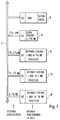
- the device 1 shows the general structure of a multiple line system which comprises a bus 11 and a plurality of data processing or data storage devices 12 to 16. These can connect to one another via the bus 11 and exchange information.
- the devices 12 to 16 can be differently constructed devices.
- the devices 12, 13 and 14 are processor units, each of which contains the signal transmitter and signal receiver S / E, a processor, an internal memory and an internal bus.
- the device 15 is a global storage unit and contains signal transmitters and signal receivers S / E and a global memory.
- the device 16 is a DMA unit and contains signal transmitters and signal receivers S / E and a DMA controller for direct memory access, which in turn can be connected to a data terminal.
- the bus 11 consists of a bundle of several signal lines, via which any two or more data processing devices can correspond with one another as desired.
- Each data processing device 12 to 16 can control the memory of another data processing device in order to exchange information with this memory, if necessary using its own memory.
- the memory of a receiving device desired by a sending device must be addressed, for which purpose the addressing method to be described below is carried out.
- an external address area is provided between the individual devices 12 to 15 and the bus 11.
- This external address area has a total address volume, which for the example shown in FIG. 1 has a size of 0 to 4 Mbytes.
- This total address volume is made up of the individual address volumes of the devices 12 to 15 together, assuming that device 12 has an internal memory with an internal address volume of 0 to 1/2 MB, device 13 has an internal memory with an address volume of 0 to 1 MB, device 14 has an internal memory with an address volume of 0 to 3/4 MB and the device 15 has global memory with an address volume of 0 to 1 3/4 MB.
- the device 16 does not contain any internal memory as a DMA unit.
- the individual address volumes of the devices 12 to 15 together form an address volume of 0 to 4 MB, which represents the external address area.
- the internal address area for the respective device 12 to 15 is formed by the internal address volume.
- the respective processor can correspond to the associated internal memory via the internal bus (J-bus).
- 2 shows a schematic, circular representation of a total address volume, which is composed of individual address volumes AV 1 , AV 2 , AV 3 ... AV n-1 , AV n .
- EA 1 an external start address
- the total address volume composed in the direction of arrow E in FIG. 1 can be understood as the sum of the address volumes of individual data processing devices, as shown in FIG. 1 at 12 to 15 are shown.
- an external start address EA is specified for each address volume AV, which corresponds to the address volume for the external address area formed by the total address volume, which is upstream of it on the circle in the direction of arrow E.
- the external start address EA 2 corresponds to the value of the address volume AV 1
- the start address EA 3 corresponds to the value of the previous address volumes, namely the sum AV 1 + AV 2 .
- the relationship then generally applies 1 also shows internal start addresses for each individual address volume AV. Each internal start address has the value 0.
- each of the data processing devices 12 to 15 (FIG. 1) is now able to generate a number of addresses which corresponds to the total address volume, as shown, for example, in FIG. 2, it is possible in the following to drive each memory cell of all data processing devices to be described directly.
- a memory cell in the address volume AV n is to be addressed from a data processing device with the address volume AV m , said memory cell having the internal address J and the external address E there.
- each data processing device Since it is assumed that each data processing device is able to generate a number of addresses which corresponds to the total address volume, and since information is available in each data processing device in a manner to be described, at which point If its address volume is arranged in the total address volume, the data processing device can use the address volume AV m to generate an address which, starting from the internal start address JA, has a value which is the sum of the address volumes in the direction of that shown by the arrow E in FIG. 2 Direction of rotation up to the external address E n or J n . The value of this address is then
- this value can be classified in the external address area and can be used uniquely to control the memory cell within the address volume AV with the internal address n J, it must be related to the external start address EA 1 . This is done in that in the transmitting data processing device the address generated in the manner described above is increased by the external start address EA m , and in that this address which is increased in this way is then transmitted via bus 11 (FIG. 1).
- the address appearing on the bus 11 and increased in the sending data processing device by its external starting address EA m is then reduced by the external starting address which corresponds to the respective data processing device.
- the received address is then reduced by the value of the start address EA n .
- the value AV a remains in the data processing device with the address volume AV n , which corresponds exactly to the value of the internal address J n to be controlled.
- FIG. 3 shows the part relevant for the transmission of an address
- FIG. 4 the part relevant for the reception of an address of a data processing device, which may have the address volume AV n within the total address volume shown in FIG. 2.
- This device contains a processor 20 and an internal memory 25 and is connected to the bus 11 via signal paths 34 and 40.
- the information exchange which takes place must be initiated by the processor 20 generating the address of a memory cell or a memory section of another data processing device.
- This address is routed to the internal bus 21, via which the processor can also correspond directly to the internal memory 25 by means of internal addresses.
- the address also reaches via the signal path 22 to the input B of a comparator 24 of the type SN7485, the input A of which is fed with a value which corresponds to the address volume AV n of the internal memory 25.
- the address generated by the processor 20 is fed via the signal path 32 to one input of an adder circuit 29 of the type SN7483, the other input of which is fed via a signal path 31 with a value which is the sum of the Address volumes correspond to the data processing devices preceding them in the order shown in FIG. 2 or their internal memory.
- This value is fixed in the data processing device, for which purpose a device 30 is used, which can also be referred to as a coding switch.
- a coding switch can be a mechanically or electronically operating switch device which, when the data processing device is installed, can be set to a value which corresponds to the start address of the internal memory 25 in the manner already described.
- the comparator 24 decides whether or not the address supplied to it via the input B fits into the address volume AV of the data processing device. If it has a larger value than the address volume AV n , a control signal is emitted via the output A ⁇ B of the comparator 24, which characterizes an external memory access. If the comparison result is less than or equal to the address volume AV, a control signal is emitted via the output A> B, which characterizes an internal access, which means that the processor 20 can correspond directly with the internal memory 25.
- the control signal emitted via the signal path 26 passes via a sequence control 28 to a transmission circuit 27, which can also be referred to as a bus driver.
- the control signal releases the output of the sum formed in the adder 29 from the generated address and the value generated with the device 30, so that the sum address thus formed, which is supplied to the bus driver 27 via the signal path 33, via the signal path 34 to the Bus 11 can be forwarded.
- the sequence control circuit 28 generates a predetermined time coordination of the connection of the bus driver 27 in accordance with the special operating mode of the multiple line system, so that the address passed via the signal path 34 to the bus 11 is forwarded in coordination or synchronization with the bus operation.
- An address which has been transmitted via the bus 11 is received with the circuit shown in FIG. 4.
- the address signals pass via the signal path 40 to a signal receiver 41, which, if amplified, feeds them to an address register 43 via the signal path 42.
- the address is fed via the signal path 47 to a summing circuit 48 of the SN 7483 type, which effects a subtraction by a value which corresponds to the start address of the internal memory 25.
- This value has already been explained with reference to FIG. 3 and is supplied to the summing circuit 48 by the device 30 via the signal path 44 as well as an inverter 45 and a signal path 46.
- the inverter 45 causes the summing circuit to carry out a subtraction, so that an address is output at its output via the signal path 49 which corresponds to the address received via the bus 11 less the value generated in the device 30.
- This reduced address goes to a comparator 50 of the type SN 7485, with which it is determined whether the address fits into the address volume AV n , which is provided for the internal memory 25. If this is the case, a control signal is issued at the output A ⁇ B of the comparator 50, which opens a gate circuit 51 so that the received address then reaches the internal memory 25 via a signal path 52.
- the gate circuit 51 is not opened, so that the internal memory 25 cannot be activated. Such control then takes place in one of the other data processing devices, in the address volume of which the received address fits. In this way, the correct data processing device is selected automatically.
- the device 30 can be a mechanical or electronic coding switch. It can also be constructed as a register, which can be set from any point in the multi-line system. It is then possible, for example, to change the value generated in each case with the device 30 by means of a program control and to carry out relocations of the data processing devices within the sequence shown in FIG. 2.
- FIG. 5 shows a circuit arrangement which operates according to the other variant provided in the context of the invention and is provided for sending an address. The reception of an address transmitted with this circuit arrangement is possible with the circuit arrangement shown in FIG. 4.
- the circuit arrangement shown in Fig. 5 operates on a principle in which each data processing device of the multi-line system regards the addresses of the memory cells of all memories as belonging to a continuous address space which begins with the start address of the memory of the first data processing device of the system.
- the address volume of the respective memory of a data processing device forms a window within the total address volume of all memories, which, for example, for the Schmea shown in FIG. 2 with the address volume AV m with the starting address begins and extends to the end address extends.
- the internal addresses of the data processing devices match the external addresses that are transmitted via the bus.
- FIG. 5 again shows the bus 11 on which addresses are to be transmitted using the circuit arrangement shown.
- the circuit arrangement is connected to the bus 11 via a signal path 54, a transmission circuit 57 being provided as in the circuit arrangement shown in FIG. 3.
- the processor 55 In order to initiate communication with a memory, the processor 55 generates an address which is fed to the two comparators 72 and 53 via the internal bus 71 of the transmission circuit 57 and to the internal memory 70 via an adding circuit 59.
- a device 60 is also provided with which, as in the circuit arrangement according to FIG. 3, the value can be delivered. This value is the comparator 53 as a comparison variable, an adder 58 as the first Summand and an inverter 56 supplied, which feeds it as the second summand of the adder circuit 59 after inverting.
- the second summand for the adder circuit 58 is the value AV n , which corresponds to the address volume of the internal memory 70.
- the comparators 72 and 53 are of the type SN7485, the adders 58 and 59 of the type SN7483.
- the address generated by the processor 55 is compared with the value in the comparator 53 compared, which is output by the device 60.
- This value corresponds to the external start address of the internal memory 70.
- the external end address of this memory 70 corresponds to the sum of the value output by the device 60 and the value AV, which is formed by the adder circuit 58. This sum is fed as a comparison variable to the comparator 72, which also carries out a comparison with the address given by the processor 55.
- the output A ⁇ B of the comparator 53 and the output A2B of the comparator 72 emit a logic 1 signal to an AND gate 61, which, in this control, sends a control signal to the internal Memory 70 emits, so that it can be controlled with the address generated by the processor 55, which was thus recognized as an internal address, after the inverted value of the external start address was previously subtracted from this address with the adder circuit 59.
- the control signal for the internal memory 70 is also fed to an inverter 62 which prevents the transmission circuit 57 from passing the address output by the processor 55 onto the bus 11.
- the address generated by the processor 55 lies outside the address volume of the internal memory 70, then either the output A ⁇ B of the comparator 53 or the output A ⁇ B of the comparator 72 or both outputs give a logic 0 signal to the AND gate 61 from. This in turn then sends a logic 0 signal to the inverter 62, which thereby activates the transmission circuit 57, so that the address given by the processor 55 reaches the bus 11 and is sent to another data processing device or to a circuit arrangement of the type shown in FIG 4 shown type can be transferred. At the same time, the internal memory 70 is blocked by the logic 0 signal of the AND gate 61 against the address from the adder circuit 59 being picked up.
Landscapes
- Engineering & Computer Science (AREA)
- Theoretical Computer Science (AREA)
- Physics & Mathematics (AREA)
- General Engineering & Computer Science (AREA)
- General Physics & Mathematics (AREA)
- Multi Processors (AREA)
- Bus Control (AREA)
- Memory System (AREA)
Abstract
Bei einem Verfahren zur Adressierung der jeweils ein Adreßvolumen aufweisenden Speicher mehrerer datenverarbeitender Einrichtungen in einem Mehrfach-Leitungssystem wird in einer eine Datenübertragungsverbindung einleitenden datenverarbeitenden Einrichtung die Adresse einer Speicherzelle des Speichers einer gewünschten datenverarbeitenden Einrichtung erzeugt und auf das Mehrfach- leitungssystem geleitet. Diese Adresse wird in jeder datenverarbeitenden Einrichtung empfangen und auf ihre Zugehörigkeit zu dem Adreßvolumen des jeweiligen Speichers überprüft. Jede der datenverarbeitenden Einrichtungen kann die Adressen der Speicherzellen aller Speicher der datenverarbeitenden Einrichtungen, bezogen auf ein mit der Anfangsadresse des Speichers der ersten datenverarbeitenden Einrichtung beginnendes kontinuierliches Gesamtadreßvolumen aller Speicher, direkt erzeugen und in jeder datenverarbeitenden Einrichtung erfolgt eine Verringerung der empfangenen bzw. der dem eigenen Speicher zuzuführende Adresse um die für diesen Speicher geltende externe Anfangsadresse.
Description
Die Erfindung betrifft ein Verfahren und eine Schaltungsanordnung zur Adressierung der jeweils ein Adreßvolumen aufweisenden Speicher mehrerer datenverarbeitender Einrichtungen in einem Mehrfachleitungssystem, bei dem in einer eine Datenübertragungsverbindung einleitenden datenverarbeitenden Einrichtung die Adresse einer Speicherzelle des Speichers einer gewünschten datenverarbeitenden Einrichtung erzeugt und auf das Mehrfachleitungssystem geleitet wird und diese Adresse in jeder datenverarbeitenden Einrichtung empfangen und auf ihre Zugehörigkeit zu dem Adreßvolumen des jeweiligen Speichers überprüft wird.The invention relates to a method and a circuit arrangement for addressing the memory, each of which has an address volume, of a plurality of data processing devices in a multiple line system, in which the address of a memory cell of the memory of a desired data processing device is generated in a data processing device initiating a data transmission connection and is passed to the multiple line system and this address is received in each data processing device and checked for its affiliation with the address volume of the respective memory.
Ein Mehrfach-Leitungssystem, an das mehrere datenverarbeitende Einrichtungen angeschlossen sind, kann auch als Multicomputersystem bezeichnet werden, wenn es sich bei den datenverarbeitenden Einrichtungen um Rechner handelt. Um die folgende Beschreibung zu vereinfachen, wird eine an ein Mehrfach-Leitungssystem anschaltbare datenverarbeitende Einrichtung auch als Prozessor bezeichnet, obwohl die Anschaltung auch anderer Arten datenverarbeitender Einrichtungen denkbar ist. Ferner wird das Mehrfach- Leitungssystem in Übereinstimmung mit der dem Fachmann geläufigen Terminologie im folgenden als "Bus" bezeichnet.A multiple line system, to which several data processing devices are connected, can also be referred to as a multicomputer system if the data processing devices are computers. In order to simplify the following description, a data processing device that can be connected to a multiple line system is also referred to as a processor, although the connection of other types of data processing devices is also conceivable. Furthermore, the multiple line system is referred to below as "bus" in accordance with the terminology familiar to the person skilled in the art.
Zu einer an einen Bus angeschlossenen datenverarbeitenden Einrichtung bzw. Prozessor kann auch ein interner Speicher gehören. Ferner können an einen Bus auch externe Speicher angeschaltet sein, die eine datenspeichernde Einrichtung darstellen, welche als Speicher mit den an den Bus angeschlossenen Prozessoren bzw. Rechnern sowie arn mit DMA-Einheiten korrespondieren können, die gleichfalls an den Bus angeschlossen sind. Eine DMA-Einheit enthält ein DMA-Gerät für direkten Speicherzugriff sowie eine zugehörige Gerätesteuerung. Sie steht mit einem Datenendgerät in Verbindung, an dem Daten eingegeben oder ausgegeben bzw. dargestellt werden können.An internal memory can also belong to a data processing device or processor connected to a bus. Furthermore, external memories can also be connected to a bus, which represent a data storage device, which is used as memory with the processors or computers connected to the bus and also with DMA units can correspond, which are also connected to the bus. A DMA unit contains a DMA device for direct memory access and associated device control. It is connected to a data terminal on which data can be entered, output or displayed.
Alle diese datenverarbeitenden Einrichtungen können über den Bus miteinander korrespondieren, d.h. Informationen austauschen, die letztlich immer bei einer sendenden Einrichtung ausgespeichert und bei einer empfangenden Einrichtung eingespeichert werden müssen. Hierzu ist eine Speicheradressierung erforderlich, wozu eine sendende Einrichtung ein Adressensignal erzeugt und auf den Bus weiterleitet, welches über den Bus übertragen wird und zu einer oder mehreren anderen Einrichtungen gelangt, wo es nach dem Empfang darauf überprüft wird, ob die mit ihm übertragene Adresseninformation zu dem Adreßvolumen des in der empfangenden Einrichtung jeweils vorhandenen Speichers gehört. Ist dies nicht der Fall, so wird in der empfangenden Einrichtung kein weiterer Schaltvorgang ausgelöst. Paßt die Adresseninformation jedoch in das Adreßvolumen des Speichers einer empfangenden Einrichtung, so ist damit die durch das Adressensignal angesteuerte Einrichtung erreicht, und der Speicher dieser Einrichtung kann dann weitere von der sendenden Einrichtung über den Bus zu übertragende Informationen aufnehmen.All of these data processing devices can correspond to one another via the bus, i.e. Exchange information that ultimately always has to be stored at a sending device and must be stored at a receiving device. This requires memory addressing, for which a sending device generates an address signal and forwards it to the bus, which is transmitted via the bus and to one or more other devices, where it is checked after receipt to determine whether the address information transmitted with it is belongs to the address volume of the memory available in the receiving device. If this is not the case, no further switching process is triggered in the receiving device. However, if the address information fits into the address volume of the memory of a receiving device, then the device controlled by the address signal is reached, and the memory of this device can then accommodate further information to be transmitted by the sending device via the bus.
Man hat nun bisher die internen Speicher von Prozessoren, die mit einem Mehrfachleitungssystem verbunden sind, selektiv derart adressiert, daß ein Adressenwort die Adresse des gewünschten Prozessors und ein weiteres Adressenwort dann die Adresse eines Speicherplatzes des in diesem Prozessor vorhandenen internen Speichers darstellt. Ein Nachteil eines solchen Adressierverfahrens besteht in der für die zweistufige Adressierung erforderlichen Zeit. Außerdem muß das Mehrfachleitungssystem für diese in zwei Schritten ablaufende Adressierung besonders aufgebaut sein, da entweder zwei zeitlich aufeinanderfolgende Schritte eine entsprechende zeitliche Steuerung der Adressierung benötigen oder aber bei gleichzeitiger Übertragung der unterschiedlichen Adreßabschnitte eigens zugeordnete Leitungsadern erforderlich sind. Ein weiterer Nachteil besteht in dem für zwei unterschiedliche Adreßabschnitte erforderlichen besonderen Steueraufwand bei der Verbindungsherstellung mit einem gewünschten Speicher.So far, the internal memories of processors which are connected to a multi-line system have been selectively addressed in such a way that an address word represents the address of the desired processor and a further address word then represents the address of a memory location of the internal memory present in this processor. A disadvantage of such an addressing method is that for the two stage addressing required time. In addition, the multi-line system for this two-step addressing must be specially designed, since either two consecutive steps require a corresponding timing of the addressing, or separately assigned line wires are required for simultaneous transmission of the different address sections. Another disadvantage is the special control effort required for two different address sections when connecting to a desired memory.
Die Aufgabe der Erfindung besteht darin, den Zeit- und Schaltungsaufwand für die Erzeugung von Adreß- und Steuersignalen herabzusetzen und eine Möglichkeit zur Adressierung der Speicher mehrerer an ein Mehrfach-Leitungssystem angeschlossener datenverarbeitender Einrichtungen anzugeben, die bei selbsttätiger direkter Adressierung des jeweils gewünschten Speichers keinen zusätzlichen Aufwand an Leitungen und Schaltungstechnik für die Übertragung von Steuersignalen verursacht.The object of the invention is to reduce the time and circuit complexity for the generation of address and control signals and to provide a possibility for addressing the memory of a plurality of data processing devices connected to a multiple line system which, with automatic direct addressing of the respectively desired memory, does not require any additional Effort in lines and circuit technology for the transmission of control signals caused.
Ein Verfahren eingangs genannter Art ist zur Lösung dieser Aufgabe erfindungsgemäß derart ausgebildet, daß jede der datenverarbeitenden Einrichtungen die Adressen der Speicherzellen aller Speicher der datenverarbeitenden Einrichtungen, bezogen auf ein mit der Anfangsadresse des Speichers der ersten datenverarbeitenden Einrichtung beginnendes kontinuierliches Gesamtadreßvolumen aller Speicher, direkt erzeugen kann und daß in jeder datenverarbeitenden Einrichtung eine Verringerung der empfangenen bzw. der dem eigenen Speicher zuzuführenden Adresse um die für diesen Speicher geltende externe Anfangsadresse erfolgt.A method of the type mentioned at the outset is designed according to the invention in such a way that each of the data processing devices can directly generate the addresses of the memory cells of all memories of the data processing devices, based on a continuous total address volume of all memories starting with the starting address of the memory of the first data processing device and that in each data processing device the received address or the address to be supplied to its own memory is reduced by the external start address valid for this memory.
Wenn man die ggf. unterschiedlich großen Adreßvolumina der Speicher der datenverarbeitenden Einrichtungen kontinuierlich aneinanderreiht, so entsteht ein Gesamtadreß- volumen, dessen Größe die Summe aller einzelnen Adreßvolumina ist. Wenn jede mit dem Mehrfach-Leitungssystem verbundene datenverarbeitende Einrichtung alle möglichen Adressen innerhalb dieses Gesamtadreßvolumens erzeugen kann, so ist die direkte Ansteuerung einer jeden im System vorhandenen Speicherzelle möglich. Die Adreßworte sind dabei zwar relativ lang, jedoch können sie in einem einzigen und nicht in zwei Steuerschritten übertragen werden, wie es bisher bei der getrennten Adressierung der jeweils gewünschten datenverarbeitenden Einrichtung und des mit ihr verbundenen Speichers erforderlich war. Unter Berücksichtigung dieses Vorteils fällt eine gegenüber der bisherigen zweiteiligen Adresse vielleicht größere Adressenlänge kaum ins Gewicht.If you string together the possibly different sized Adreßvolumina the memory of the data processing units continuously, then a Gesamtadreß - volume whose size is the sum of all individual Adreßvolumina. If each data processing device connected to the multi-line system can generate all possible addresses within this total address volume, the direct control of each memory cell present in the system is possible. The address words are relatively long, but they can be transmitted in a single and not in two control steps, as was previously required for the separate addressing of the desired data processing device and the memory connected to it. Taking this advantage into account, a longer address length than the previous two-part address is hardly significant.
Für die praktische Durchführung des Verfahrens nach der Erfindung kommen unterschiedliche Wege in Betracht, die sich je nach besonderen Anforderungen hinsichtlich Schaltungsaufwand oder Systemstruktur einsetzen lassen. Weiter unten werden anhand der Figuren zwei derartige Möglichkeiten erläutert, von denen die eine allgemein dem Lösungsweg des Patentanspruchs 1 entspricht.For the practical implementation of the method according to the invention there are different ways that can be used depending on the particular requirements with regard to circuit complexity or system structure. Two such possibilities are explained below with the aid of the figures, one of which generally corresponds to the solution of
Demgegenüber läßt sich eine weitere Verringerung schaltungstechnischen Aufwandes erzielen, wenn die Weiterbildung gemäß Patentanspruch 2 angewendet wird. Hierbei wird die jeweils von einer datenverarbeitenden Einrichtung abzugebende Adresse vor ihrer Weiterleitung über den Bus in ganz bestimmter Weise aufgebaut. Hierzu wird davon ausgegangen, daß innerhalb des kontinuierlichen Gesamtadreßvolumens das Adreßvolumen des Speichers der jeweils sendenden datenverarbeitenden Einrichtung eine bestimmte Lage hat, da das Gesamtadreßvolumen durch Aneinanderreihung der Einzeladreßvolumina entstanden ist.Wenn nun das Gesamtadreßvolumen, von jeder einzelnen datenverarbeitenden Einrichtung aus gesehen, bei der Anfangsadresse des zu dieser Einrichtung gehörenden Speichers beginnt, so ist die in dieser datenverarbeitenden Einrichtung erzeugte Adresse einer Speicherzelle in einer anderen datenverarbeitenden Einrichtung auf diese Anfangsadresse bezogen, so daß jede Speicherzelle aller Speicher des Systems durch eine von der Lage des jeweiligen Prozessors im System abhängige Adresse angesteuert wird, was bedeutet, daß zunächst eine Zweideutigkeit bei der Adressierung von Speicherzellen besteht. Um diese Zweideutigkeit zu beseitigen, muß die jeweils abzugebende Adresse in der sendenden datenverarbeitenden Einrichtung so umgesetzt werden, daß sie bei Übertragung über den Bus nur in einer der anderen datenverarbeitenden Einrichtungen als Ansteueradresse für den zugehörigen Speicher ausgewertet wird. Dies erfolgt nun dadurch, daß die zu übertragende Adresse, die zunächst auf die interne Anfangsadresse des Speichers des sendenden Prozessors bezogen ist, um den Wert der externen Anfangsadresse dieses Speichers erhöht wird, wobei diese externe Anfangsadresse aber auf ein mit der Anfangsadresse des Speichers der ersten datenverarbeitenden Einrichtung beginnendes Gesamtadreßvolumen bezogen ist. Die so erhöhte Adresse wird dann über den Bus übertragen und ist in jedem Falle auf ein Gesamtadreßvolumen bezogen, welches, vom Bus her gesehen, für alle datenverarbeitenden Einrichtungen gleich ist und dieselbe Anfangsadresse aufweist. Wenn die so übertragene Adresse auf die empfangsbereiten datenverarbeitenden Einrichtungen gelangt, so wird sie dort jeweils überprüft. Diese Überprüfung erfolgt erst dann, wenn in jeder datenverarbeitenden Einrichtung eine Verringerung der empfangenen Adresse vorgenommen ist. Diese Verringerung erfolgt um einen Wert, der der für den Speicher der jeweils prüfenden datenverarbeitenden Einrichtung maßgebenden externen Anfangsadresse entspricht.In contrast, a further reduction in circuit complexity can be achieved if the training according to
Wie noch anhand eines Ausführungsbeispiels beschrieben wird, geschieht nach diesem Verfahren in jedem Falle eine eindeutige und direkte Ansteuerung der jeweils gewünschten Speicherzelle ohne zusätzliche mehrschrittige Steuervorgänge. Die jeweils erzeugte Adresse durchläuft vor dem Senden bzw. nach dem Empfangen im jeweiligen Prozessor lediglich einen Additions- bzw. Subtraktionsschritt, ohne daß aufwendige mehrschrittige Decodierungen oder Voradressierungen bzw. Adreßzuordnungen erforderlich sind.As will be described with reference to an exemplary embodiment, this method always leads to a clear and direct control of the desired memory cell without additional multi-step control processes. The address generated in each case only goes through an addition or subtraction step in the respective processor before sending or after receiving, without complex multi-step decoding or pre-addressing or address assignments being necessary.
Weiterbildungen der Erfindung sowie Schaltungen zu ihrer Durchführung werden aus der folgenden Figurenbeschreibung ersichtlich. Im einzelnen zeigen:
- Fig. 1 den allgemeinen Aufbau eines Mehrfach-Leitungssystems mit datenverarbeitenden Einrichtungen,
- Fig. 2 ein bei einem Verfahren nach der Erfindung angewandtes Prinzip der Adreßerzeugung,
- Fig. 3 ein Ausführungsbeispiel einer Schaltung zur Durchführung des erfindungsgemäßen Verfahrens gemäß einer ersten Variante bei einer sendenden Datenverarbeitungseinrichtung,
- Fig. 4 ein Ausführungsbeispiel einer Schaltung zur Durchführung der ersten Variante des erfindungsgemäßen Verfahrens bei einer empfangenden Datenverarbeitungseinrichtung und
- Fig. 5 ein Ausführungsbeispiel einer Schaltung zur Durchführung des erfindungsgemäßen Verfahrens gemäß einer zweiten Variante bei einer sendenden Datenverarbeitungseinrichtung.
- 1 shows the general structure of a multiple line system with data processing devices,
- 2 shows a principle of address generation applied in a method according to the invention,
- 3 shows an exemplary embodiment of a circuit for carrying out the method according to the invention in accordance with a first variant in the case of a sending data processing device,
- Fig. 4 shows an embodiment of a circuit for performing the first variant of the method according to the invention in a receiving data processing device and
- Fig. 5 shows an embodiment of a circuit for performing the method according to the invention according to a second variant in a sending data processing device.
In Fig. 1 ist der allgemeine Aufbau eines Mehrfach-Leitungssystems dargestellt, das einen Bus 11 und mehrere datenverarbeitende bzw. datenspeichernde Einrichtungen 12 bis 16 umfaßt. Diese können über den Bus 11 miteinander in Verbindung treten und Informationen austauschen. Bei den Einrichtungen 12 bis 16 kann es sich um unterschiedlich aufgebaute Einrichtungen handeln. So sind beispielsweise die Einrichtungen 12, 13 und 14 Prozessoreinheiten, die jeweils Signalsender und Signalempfänger S/E, einen Prozessor, einen internen Speicher und einen internen Bus enthalten. Die Einrichtung 15 ist eine globale Speichereinheit und enthält Signalsender und Signalempfänger S/E sowie einen globalen Speicher. Die Einrichtung 16 ist eine DMA-Einheit und enthält Signalsender und Signalempfänger S/E sowie eine DMA-Steuerung für direkten Speicherzugriff, die ihrerseits mit einem Datenendgerät in Verbindung stehen kann. Der Bus 11 besteht aus einem Bündel mehrerer Signalleitungen, über die ein beliebiges Korrespondieren zweier oder mehrerer datenverarbeitender Einrichtungen untereinander möglich ist. Jede datenverarbeitende Einrichtung 12 bis 16 kann den Speicher einer anderen datenverarbeitenden Einrichtung ansteuern, um mit diesem Speicher ggf. unter Hinzuziehung des eigenen Speichers Informationen auszutauschen. Hierzu muß der von einer sendenden Einrichtung jeweils gewünschte Speicher einer empfangenden Einrichtung adressiert werden, wozu das im folgenden zu beschreibende Adressierungsverfahren durchgeführt wird.1 shows the general structure of a multiple line system which comprises a
Hierzu sei zunächst die Organisation der Adreßvolumina der einzelnen Einrichtungen erläutert. Wie Fig. 1 zeigt, ist ein externer Adreßbereich zwischen den einzelnen Einrichtungen 12 bis 15 und dem Bus 11 vorgesehen. Dieser externe Adreßbereich hat ein Gesamtadreßvolumen, das für das in Fig. 1 gezeigte Beispiel einen Umfang von 0 bis 4 MByte hat. Dieses Gesamtadreßvolumen setzt sich aus den einzelnen Adreßvolumina der Einrichtungen 12 bis 15 zusammen, wobei angenommen sei, daß die Einrichtung 12 einen internen Speicher mit einem internen Adreßvolumen von 0 bis 1/2 MB, die Einrichtung 13 einen internen Speicher mit einem Adreßvolumen von 0 bis 1 MB, die Einrichtung 14 einen internen Speicher mit einem Adreßvolumen von 0 bis 3/4 MB und die Einrichtung 15 einen globalen Speicher mit einem Adreßvolumen von 0 bis 1 3/4 MB hat. Die Einrichtung 16 enthält als DMA-Einheit keinen internen Speicher.For this purpose, the organization of the address volumes of the individual facilities is explained first. As shown in FIG. 1, an external address area is provided between the
Anhand der Fig. 1 ist zu erkennen, daß die einzelnen Adreßvolumina der Einrichtungen 12 bis 15 ingesamt ein Adreßvolumen von 0 bis 4 MB bilden, welches den externen Adreßbereich darstellt. Der interne Adreßbereich ist für die jeweilige Einrichtung 12 bis 15 durch das interne Adreßvolumen gebildet. Innerhalb dieses internen Adreßvolumens kann der jeweilige Prozessor mit dem jeweils zugehörigen internen Speicher über den internen Bus (J-Bus) korrespondieren.1 that the individual address volumes of the
Anhand der Fig. 2 soll nun erläutert werden, wie die Adressierung des Speichers einer datenverarbeitenden Einrichtung von einer sendenden Einrichtung her über den Bus erfolgt, indem das erfindungsgemäße Verfahren angewendet wird. Fig. 2 zeigt hierzu eine schematische, kreisförmige Darstellung eines Gesamtadreßvolumens, welches sich aus einzelnen Adreßvolumina AV1, AV2, AV3... AVn-1, AV n zusammensetzt. Für dieses Gesamtadreßvolumen![]()

![]()
Wenn nun jede der datenverarbeitenden Einrichtungen 12 bis 15 (Fig. 1) in der Lage ist, eine Anzahl von Adressen zu erzeugen, die dem Gesamtadreßvolumen entspricht, wie es beispielsweise in Fig. 2 dargestellt ist, so ist es möglich, in der im folgenden zu beschreibenden Weise jede Speicherzelle sämtlicher datenverarbeitender Einrichtungen direkt anzusteuern. Hierzu sei beispielsweise angenommen, daß gemäß dem in Fig. 2 schematisch angedeuteten Verbindungsweg C aus einer datenverarbeitenden Einrichtung mit dem Adreßvolumen AVm eine Speicherzelle im Adreßvolumen AVn adressiert werden soll, die dort die interne Adresse J und die externe Adresse E hat.If each of the
Da voraussetzungsgemäß jede datenverarbeitende Einrichtung in der Lage ist, eine Zahl von Adressen zu erzeugen, die dem Gesamtadreßvolumen entspricht, und da in jeder datenverarbeitenden Einrichtung in noch zu beschreibender Weise eine Information darüber vorliegt, an welcher Stelle ihr Adreßvolumen in das Gesamtadreßvolumen eingeordnet ist, kann die datenverarbeitende Einrichtung mit dem Adreßvolumen AVm eine Adresse erzeugen, die ausgehend von der internen Anfangsadresse JA einen Wert hat, der der Summe der Adreßvolumina in Richtung des in Fig. 2 durch den Pfeil E gezeigten Umlaufsinnes bis zur externen Adresse En bzw. Jn entspricht. Der Wert dieser Adresse beträgt dannSince it is assumed that each data processing device is able to generate a number of addresses which corresponds to the total address volume, and since information is available in each data processing device in a manner to be described, at which point If its address volume is arranged in the total address volume, the data processing device can use the address volume AV m to generate an address which, starting from the internal start address JA, has a value which is the sum of the address volumes in the direction of that shown by the arrow E in FIG. 2 Direction of rotation up to the external address E n or J n . The value of this address is then

In allen mit dem Bus 11 verbundenen datenverarbeitenden Einrichtungen wird dann die auf dem Bus 11 erscheinende und in der sendenden datenverarbeitenden Einrichtung um deren externe Anfangsadresse EAm erhöhte Adresse um die externe Anfangsadresse vermindert, die der jeweiligen datenverarbeitenden Einrichtung entspricht. Im Falle der Einrichtung mit dem Adreßvolumen AVn wird dann die empfangene Adresse um den Wert der Anfangsadresse EAn verringert. Es ergibt sich dann die folgende Rechnung
Somit bleibt als Ergebnis dieser vorstehend beschriebenen Schritte in der datenverarbeitenden Einrichtung mit dem Adreßvolumen AVn der Wert AVa übrig, der genau dem Wert der anzusteuernden internen Adresse Jn entspricht.Thus, as a result of these steps described above, the value AV a remains in the data processing device with the address volume AV n , which corresponds exactly to the value of the internal address J n to be controlled.
Im folgenden wird anhand der Fig. 3 und 4 die Funktion von Schaltungen beschrieben, mit denen das erfindungsgemäße Verfahren innerhalb einer datenverarbeitenden Einrichtung durchgeführt werden kann, die einer der in Fig. 1 gezeigten Einrichtungen 12 bis 14 entsprechen kann. Fig. 3 zeigt den für das Aussenden einer Adresse relevanten Teil, Fig. 4 den für das Empfangen einer Adresse relevanten Teil einer datenverarbeitenden Einrichtung, die innerhalb des in Fig. 2 gezeigten Gesamtadreßvolumens das Adreßvolumen AVn haben möge. Diese Einrichtung enthält einen Prozessor 20 und einen internen Speicher 25 und ist mit dem Bus 11 über Signalwege 34 und 40 verbunden.The function of circuits with which the method according to the invention can be carried out within a data processing device, which can correspond to one of the
Wenn die datenverarbeitende Einrichtung über den Bus 11 mit einer anderen datenverarbeitenden Einrichtung in Verbindung treten soll, so muß der dabei erfolgende Informationsaustausch dadurch eingeleitet werden, daß der Prozessor 20 die Adresse einer Speicherzelle bzw. eines Speicherabschnitts einer anderen datenverarbeitenden Einrichtung erzeugt. Diese Adresse wird auf den internen Bus 21 geleitet, über den der Prozessor auch mittels interner Adressen direkt mit dem internen Speicher 25 korrespondieren kann. Die Adresse gelangt dabei über den Signalweg 22 auch auf den Eingang B eines Vergleichers 24 vom Typ SN7485, dessen Eingang A mit einem Wert gespeist wird, der dem Adreßvolumen AVn des internen Speichers 25 entspricht. Außerdem wird die von dem Prozessor 20 erzeugte Adresse über den Signalweg 32 dem einen Eingang einer Addierschaltung 29 vom Typ SN7483 zugeführt,deren anderer Eingang über einen Signalweg 31 mit einem Wert gespeist wird, der der Summe der Adreßvolumina der in der in Fig. 2 gezeigten Ordnung vorhergehenden datenverarbeitenden Einrichtungen bzw. deren interner Speicher entspricht. Dieser Wert ist in der datenverarbeitenden Einrichtung fest eingestellt, wozu eine Vorrichtung 30 dient, die auch als Codierschalter bezeichnet werden kann. Ein solcher Codierschalter kann eine mechanisch oder elektronisch arbeitende Schaltervorrichtung sein, die bei der Installation der datenverarbeitenden Einrichtung auf einen Wert einstellbar ist, der in bereits beschriebener Weise der Anfangsadresse des internen Speichers 25 entspricht.If the data processing device is to be connected to another data processing device via the
Der Vergleicher 24 entscheidet, ob die ihm über den Eingang B zugeführte Adresse in das Adreßvolumen AV der datenverarbeitenden Einrichtung paßt oder nicht. Wenn sie einen größeren Wert als das Adreßvolumen AV n hat, so wird über den Ausgang A<B des Vergleichers 24 ein Steuersignal abgegeben, welches einen externen Speicherzugriff kennzeichnet. Ist das Vergleichsergebnis kleiner oder gleich dem Adreßvolumen AV , so wird über den Ausgang A>B ein Steuersignal abgegeben, welches einen internen Zugriff kennzeichnet, was besagt, daß der Prozessor 20 direkt mit dem internen Speicher 25 korrespondieren kann.The comparator 24 decides whether or not the address supplied to it via the input B fits into the address volume AV of the data processing device. If it has a larger value than the address volume AV n , a control signal is emitted via the output A <B of the comparator 24, which characterizes an external memory access. If the comparison result is less than or equal to the address volume AV, a control signal is emitted via the output A> B, which characterizes an internal access, which means that the
Das über den Signalweg 26 abgegebene Steuersignal gelangt über eine Ablaufsteuerung 28 auf eine Sendeschaltung 27, die auch als Bustreiber zu bezeichnen ist. Das Steuersignal gibt die Ausgabe der in der Addierschaltung 29 gebildete Summe aus der erzeugten Adresse und den mit der Vorrichtung 30 erzeugten Wert frei, so daß die so gebildete Summenadresse, die über den Signalweg 33 dem Bustreiber 27 zugeführt wird, über den Signalweg 34 auf den Bus 11 weitergeleitet werden kann.The control signal emitted via the
Die Ablaufsteuerschaltung 28 erzeugt eine vorgegebene zeitliche Koordination der Durchschaltung des Bustreibers 27 in Übereinstimmung mit der speziellen Betriebsart des Mehrfachleitungssystems, so daß die über den Signalweg 34 auf den Bus 11 geleitete Adresse in Abstimmung bzw. Synchronisation mit dem Busbetrieb weitergeleitet wird.The sequence control circuit 28 generates a predetermined time coordination of the connection of the
Der Empfang einer Adresse, die über den Bus 11 übertragen wurde, erfolgt mit der in Fig. 4 gezeigten Schaltung. Die Adressensignale gelangen über den Signalweg 40 auf einen Signalempfänger 41, der sie ggf. nach Verstärkung über den Signalweg 42 einem Adreßregister 43 zuführt. Aus dem Adreßregister 43 wird die Adresse über den Signalweg 47 einer Summierschaltung 48 vom Typ SN 7483 zugeführt, die eine Subtraktion um einen Wert bewirkt, der der Anfangsadresse des internen Speichers 25 entspricht. Dieser Wert wurde anhand der Fig. 3 bereits erläutert und wird von der Vorrichtung 30 über den Signalweg 44 sowie einen Inverter 45 und einen Signalweg 46 der Summierschaltung 48 zugeführt. Der Inverter 45 bewirkt durch Invertieren, daß die Summierschaltung eine Subtraktion vornimmt, so daß an ihrem Ausgang über den Signalweg 49 eine Adresse abgegeben wird, die der über den Bus 11 empfangenen Adresse, vermindert um den in der Vorrichtung 30 erzeugten Wert, entspricht. Diese verminderte Adresse gelangt auf einen Vergleicher 50 vom Typ SN 7485, mit dem festgestellt wird, ob die Adresse in das Adreßvolumen AVn paßt, welches für den internen Speicher 25 vorgesehen ist. Ist dies der Fall, so wird an dem Ausgang A<B des Vergleichers 50 ein Steuersignal abgegeben, welches eine Torschaltung 51 öffnet, so daß die empfangene Adresse dann über einen Signalweg 52 zum internen Speicher 25 gelangt.An address which has been transmitted via the
Wenn der Vergleicher 50 feststellt, daß die empfangene Adresse nicht in das Adreßvolumen AV paßt, so wird die Torschaltung 51 nicht geöffnet, so daß der interne Speicher 25 nicht angesteuert werden kann. Eine solche Ansteuerung erfolgt dann in einer der anderen datenverarbeitenden Einrichtungen, in deren Adreßvolumen die empfangene Adresse paßt. auf diese Weise erfolgt automatisch die Auswahl der jeweils richtigen datenverarbeitenden Einrichtung.If the
Die Vorrichtung 30 kann, wie beschrieben, ein mechanischer oder elektronischer Codierschalter sein. Sie kann auch als Register aufgebaut sein, welches von einer beliebigen Stelle des Mehrfachleitungssystems aus eingestellt werden kann. Es ist dann beispielsweise möglich, durch eine Programmsteuerung den jeweils mit der Vorrichtung 30 erzeugten Wert zu verändern und Verlagerungen der datenverarbeitenden Einrichtungen innerhalb der in Fig. 2 gezeigten Reihenfolge vorzunehmen.As described, the
In Fig. 5 ist eine Schaltungsanordnung dargestellt, die nach der anderen im Rahmen der Erfindung vorgesehenen Variante arbeitet und für das Aussenden einer Adresse vorgesehen ist. Der Empfang einer mit dieser Schaltungsanordnung ausgesendeten Adresse ist mit der in Fig. 4 gezeigten Schaltungsanordnung möglich.5 shows a circuit arrangement which operates according to the other variant provided in the context of the invention and is provided for sending an address. The reception of an address transmitted with this circuit arrangement is possible with the circuit arrangement shown in FIG. 4.
Die in Fig. 5 dargestellte Schaltungsanordnung arbeitet nach einem Prinzip, bei dem jede datenverarbeitende Einrichtung des Mehrfach-Leitungssystems die Adressen der Speicherzellen aller Speicher als zu einem kontinuierlichen Adreßraum gehörig betrachtet, der mit der Anfangsadresse des Speichers der ersten datenverarbeitenden Einrichtung des Systems beginnt.The circuit arrangement shown in Fig. 5 operates on a principle in which each data processing device of the multi-line system regards the addresses of the memory cells of all memories as belonging to a continuous address space which begins with the start address of the memory of the first data processing device of the system.
Bei dieser Organisation bildet das Adreßvolumen des jeweiligen Speichers einer datenverarbeitenden Einrichtung innerhalb des Gesamtadreßvolumens aller Speicher ein Fenster, welches beispielsweise für das in Fig. 2 gezeigte Schmea bei dem Adreßvolumen AVm mit der Anfangsadresse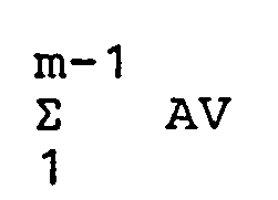

In Fig. 5 ist wiederum der Bus 11 dargestellt, auf den mit der gezeigten Schaltungsanordnung Adressen zu übertragen sind. Die Schaltungsanordnung ist mit dem Bus 11 über einen Signalweg 54 verbunden, wobei wie bei der in Fig. 3 gezeigten Schaltungsanordnung eine Sendeschaltung 57 vorgesehen ist. Der Prozessor 55 erzeugt zur Einleitung einer Kommunikation mit einem Speicher eine Adresse, die über den internen Bus 71 der Sendeschaltung 57 zwei Vergleichern 72 und 53 und über eine Addierschaltung 59 dem internen Speicher 70 zugeführt wird. Es ist auch eine Vorrichtung 60 vorgesehen, mit der wie bei der Schaltungsanordnung nach Fig. 3 der Wert
Der zweite Summand für die Addierschaltung 58 ist der Wert AVn, der dem Adreßvolumen des internen Speichers 70 entspricht.The second summand for the
Die Vergleicher 72 und 53 sind vom Typ SN7485, die Addierschaltungen 58 und 59 vom Typ SN7483.The
Die von dem Prozessor 55 erzeugte Adresse wird im Vergleicher 53 mit dem Wert
Liegt die von dem Prozessor 55 erzeugte Adresse außerhalb des Adreßvolumens des internen Speichers 70, so geben entweder der Ausgang A<B des-Vergleichers 53 oder der Ausgang A≥B des Vergleichers 72 oder beide Ausgänge ein logisches 0-Signal an das UND-Glied 61 ab. Dieses gibt dann wiederum ein logisches 0-Signal an den Inverter 62, welcher dadurch die Sendeschaltung 57 wirksam schaltet, so daß die von dem Prozessor 55 abgegebene Adresse auf den Bus 11 gelangt und an eine andere datenverarbeitende Einrichtung bzw. an eine Schaltungsanordnung der in Fig. 4 gezeigten Art übertragen werden kann. Gleichzeitig wird der interne Speicher 70 durch das logische 0-Signal des UND-Gliedes 61 gegen eine Aufnahme der Adresse aus der Addierschaltung 59 gesperrt.If the address generated by the
Claims (7)
Applications Claiming Priority (2)
| Application Number | Priority Date | Filing Date | Title |
|---|---|---|---|
| DE3300699A DE3300699C2 (en) | 1983-01-11 | 1983-01-11 | Circuit arrangement for addressing the memory of a plurality of data processing devices, each having an address volume, in a multiprocessor system with a system bus |
| DE3300699 | 1983-01-11 |
Publications (3)
| Publication Number | Publication Date |
|---|---|
| EP0115609A2 true EP0115609A2 (en) | 1984-08-15 |
| EP0115609A3 EP0115609A3 (en) | 1985-11-21 |
| EP0115609B1 EP0115609B1 (en) | 1989-05-24 |
Family
ID=6188053
Family Applications (1)
| Application Number | Title | Priority Date | Filing Date |
|---|---|---|---|
| EP83112706A Expired EP0115609B1 (en) | 1983-01-11 | 1983-12-16 | Addressing device for the storage of several data processing units in a bus system |
Country Status (4)
| Country | Link |
|---|---|
| US (1) | US4829420A (en) |
| EP (1) | EP0115609B1 (en) |
| JP (2) | JPS59144970A (en) |
| DE (2) | DE3300699C2 (en) |
Cited By (2)
| Publication number | Priority date | Publication date | Assignee | Title |
|---|---|---|---|---|
| EP0265905A2 (en) * | 1986-10-27 | 1988-05-04 | Dieter Dr. Weiss | Addressing device for modules |
| US5349650A (en) * | 1990-10-08 | 1994-09-20 | Mitsubishi Denki Kabushiki Kaisha | Address translating apparatus for translating virtual address into real address without depending on processing by CPU |
Families Citing this family (34)
| Publication number | Priority date | Publication date | Assignee | Title |
|---|---|---|---|---|
| JP2628079B2 (en) * | 1988-11-25 | 1997-07-09 | 三菱電機株式会社 | Direct memory access controller in multiprocessor system |
| US5241642A (en) * | 1989-09-28 | 1993-08-31 | Pixel Semiconductor, Inc. | Image memory controller for controlling multiple memories and method of operation |
| US5317721A (en) * | 1989-11-06 | 1994-05-31 | Zenith Data Systems Corporation | Method and apparatus to disable ISA devices for EISA addresses outside the ISA range |
| JP4651790B2 (en) * | 2000-08-29 | 2011-03-16 | 株式会社ガイア・システム・ソリューション | Data processing device |
| JP4783527B2 (en) * | 2001-01-31 | 2011-09-28 | 株式会社ガイア・システム・ソリューション | Data processing system, data processing apparatus, and control method thereof |
| US20020152061A1 (en) * | 2001-04-06 | 2002-10-17 | Shintaro Shimogori | Data processing system and design system |
| US7020788B2 (en) * | 2001-06-01 | 2006-03-28 | Microchip Technology Incorporated | Reduced power option |
| US6985986B2 (en) * | 2001-06-01 | 2006-01-10 | Microchip Technology Incorporated | Variable cycle interrupt disabling |
| US7007172B2 (en) * | 2001-06-01 | 2006-02-28 | Microchip Technology Incorporated | Modified Harvard architecture processor having data memory space mapped to program memory space with erroneous execution protection |
| US6952711B2 (en) * | 2001-06-01 | 2005-10-04 | Microchip Technology Incorporated | Maximally negative signed fractional number multiplication |
| US6601160B2 (en) | 2001-06-01 | 2003-07-29 | Microchip Technology Incorporated | Dynamically reconfigurable data space |
| US6552625B2 (en) | 2001-06-01 | 2003-04-22 | Microchip Technology Inc. | Processor with pulse width modulation generator with fault input prioritization |
| US6604169B2 (en) | 2001-06-01 | 2003-08-05 | Microchip Technology Incorporated | Modulo addressing based on absolute offset |
| US20030028696A1 (en) * | 2001-06-01 | 2003-02-06 | Michael Catherwood | Low overhead interrupt |
| US6976158B2 (en) * | 2001-06-01 | 2005-12-13 | Microchip Technology Incorporated | Repeat instruction with interrupt |
| US6937084B2 (en) * | 2001-06-01 | 2005-08-30 | Microchip Technology Incorporated | Processor with dual-deadtime pulse width modulation generator |
| US6975679B2 (en) * | 2001-06-01 | 2005-12-13 | Microchip Technology Incorporated | Configuration fuses for setting PWM options |
| US20030005269A1 (en) * | 2001-06-01 | 2003-01-02 | Conner Joshua M. | Multi-precision barrel shifting |
| US20020184566A1 (en) * | 2001-06-01 | 2002-12-05 | Michael Catherwood | Register pointer trap |
| US20030005268A1 (en) * | 2001-06-01 | 2003-01-02 | Catherwood Michael I. | Find first bit value instruction |
| US7003543B2 (en) * | 2001-06-01 | 2006-02-21 | Microchip Technology Incorporated | Sticky z bit |
| US6934728B2 (en) * | 2001-06-01 | 2005-08-23 | Microchip Technology Incorporated | Euclidean distance instructions |
| US6728856B2 (en) | 2001-06-01 | 2004-04-27 | Microchip Technology Incorporated | Modified Harvard architecture processor having program memory space mapped to data memory space |
| US7467178B2 (en) * | 2001-06-01 | 2008-12-16 | Microchip Technology Incorporated | Dual mode arithmetic saturation processing |
| US20030023836A1 (en) * | 2001-06-01 | 2003-01-30 | Michael Catherwood | Shadow register array control instructions |
| JP2003005958A (en) * | 2001-06-25 | 2003-01-10 | Pacific Design Kk | Data processor and method for controlling the same |
| JP5372307B2 (en) * | 2001-06-25 | 2013-12-18 | 株式会社ガイア・システム・ソリューション | Data processing apparatus and control method thereof |
| JP4865960B2 (en) * | 2001-06-25 | 2012-02-01 | 株式会社ガイア・システム・ソリューション | Data processing apparatus and control method thereof |
| US20040021483A1 (en) * | 2001-09-28 | 2004-02-05 | Brian Boles | Functional pathway configuration at a system/IC interface |
| US6552567B1 (en) | 2001-09-28 | 2003-04-22 | Microchip Technology Incorporated | Functional pathway configuration at a system/IC interface |
| US6993674B2 (en) * | 2001-12-27 | 2006-01-31 | Pacific Design, Inc. | System LSI architecture and method for controlling the clock of a data processing system through the use of instructions |
| US20030163674A1 (en) * | 2002-02-26 | 2003-08-28 | Mitsumasa Yoshimura | Data processing apparatus, processor unit and debugging unit |
| JP4120631B2 (en) * | 2004-10-05 | 2008-07-16 | 株式会社日立製作所 | Semiconductor integrated circuit |
| US7765250B2 (en) * | 2004-11-15 | 2010-07-27 | Renesas Technology Corp. | Data processor with internal memory structure for processing stream data |
Citations (4)
| Publication number | Priority date | Publication date | Assignee | Title |
|---|---|---|---|---|
| AT354783B (en) * | 1978-02-07 | 1980-01-25 | Bruno Dr Buchberger | PROGRAMMABLE CIRCUIT FOR DATA PROCESSING |
| US4253144A (en) * | 1978-12-21 | 1981-02-24 | Burroughs Corporation | Multi-processor communication network |
| US4315310A (en) * | 1979-09-28 | 1982-02-09 | Intel Corporation | Input/output data processing system |
| EP0106556A1 (en) * | 1982-09-30 | 1984-04-25 | Western Electric Company, Incorporated | Multiprocessor computing system featuring shared global control |
Family Cites Families (21)
| Publication number | Priority date | Publication date | Assignee | Title |
|---|---|---|---|---|
| US3292151A (en) * | 1962-06-04 | 1966-12-13 | Ibm | Memory expansion |
| US3323109A (en) * | 1963-12-30 | 1967-05-30 | North American Aviation Inc | Multiple computer-multiple memory system |
| US3555513A (en) * | 1967-10-11 | 1971-01-12 | Burroughs Corp | Multiprocessor digital computer system with address modification during program execution |
| US4025903A (en) * | 1973-09-10 | 1977-05-24 | Computer Automation, Inc. | Automatic modular memory address allocation system |
| JPS586973B2 (en) * | 1975-02-20 | 1983-02-07 | パナフアコム カブシキガイシヤ | Memory load bunch access Seigiyohoshiki |
| US4001786A (en) * | 1975-07-21 | 1977-01-04 | Sperry Rand Corporation | Automatic configuration of main storage addressing ranges |
| US4030073A (en) * | 1975-11-05 | 1977-06-14 | Digital Equipment Corporation | Initialization circuit for establishing initial operation of a digital computer |
| US4040029A (en) * | 1976-05-21 | 1977-08-02 | Rca Corporation | Memory system with reduced block decoding |
| US4096571A (en) * | 1976-09-08 | 1978-06-20 | Codex Corporation | System for resolving memory access conflicts among processors and minimizing processor waiting times for access to memory by comparing waiting times and breaking ties by an arbitrary priority ranking |
| US4398248A (en) * | 1980-10-20 | 1983-08-09 | Mcdonnell Douglas Corporation | Adaptive WSI/MNOS solid state memory system |
| US4155119A (en) * | 1977-09-21 | 1979-05-15 | Sperry Rand Corporation | Method for providing virtual addressing for externally specified addressed input/output operations |
| US4285039A (en) * | 1978-03-28 | 1981-08-18 | Motorola, Inc. | Memory array selection mechanism |
| US4189767A (en) * | 1978-06-05 | 1980-02-19 | Bell Telephone Laboratories, Incorporated | Accessing arrangement for interleaved modular memories |
| US4236207A (en) * | 1978-10-25 | 1980-11-25 | Digital Equipment Corporation | Memory initialization circuit |
| US4318175A (en) * | 1979-08-13 | 1982-03-02 | Bunker Ramo Corporation | Addressing means for random access memory system |
| IT1126475B (en) * | 1979-12-03 | 1986-05-21 | Honeywell Inf Systems | COMMUNICATION APPARATUS BETWEEN MORE PROCESSORS |
| US4392200A (en) * | 1980-01-28 | 1983-07-05 | Digital Equipment Corporation | Cached multiprocessor system with pipeline timing |
| US4365294A (en) * | 1980-04-10 | 1982-12-21 | Nizdorf Computer Corporation | Modular terminal system using a common bus |
| US4366537A (en) * | 1980-05-23 | 1982-12-28 | International Business Machines Corp. | Authorization mechanism for transfer of program control or data between different address spaces having different storage protect keys |
| IT1142074B (en) * | 1981-11-24 | 1986-10-08 | Honeywell Inf Systems | DATA PROCESSING SYSTEM WITH AUTOMATIC ALLOCATION OF THE ADDRESS IN A MODULAR MEMORY |
| US4679167A (en) * | 1983-07-29 | 1987-07-07 | Hewlett-Packard Company | Apparatus for locating a memory module within a memory space |
-
1983
- 1983-01-11 DE DE3300699A patent/DE3300699C2/en not_active Expired
- 1983-12-16 EP EP83112706A patent/EP0115609B1/en not_active Expired
- 1983-12-16 DE DE8383112706T patent/DE3379919D1/en not_active Expired
-
1984
- 1984-01-09 JP JP59000924A patent/JPS59144970A/en active Pending
-
1987
- 1987-06-29 US US07/065,120 patent/US4829420A/en not_active Expired - Fee Related
-
1988
- 1988-07-11 JP JP1988091041U patent/JPH0138695Y2/ja not_active Expired
Patent Citations (4)
| Publication number | Priority date | Publication date | Assignee | Title |
|---|---|---|---|---|
| AT354783B (en) * | 1978-02-07 | 1980-01-25 | Bruno Dr Buchberger | PROGRAMMABLE CIRCUIT FOR DATA PROCESSING |
| US4253144A (en) * | 1978-12-21 | 1981-02-24 | Burroughs Corporation | Multi-processor communication network |
| US4315310A (en) * | 1979-09-28 | 1982-02-09 | Intel Corporation | Input/output data processing system |
| EP0106556A1 (en) * | 1982-09-30 | 1984-04-25 | Western Electric Company, Incorporated | Multiprocessor computing system featuring shared global control |
Non-Patent Citations (3)
| Title |
|---|
| COMPUTER DESIGN, Band 20, Nr. 10, Oktober 1981, Seiten 179-184, Winchester, Mass., US; W.S. ANG: "Common element key to multiprocessors architecture" * |
| IBM TECHNICAL DISCLOSURE BULLETIN, Band 22, Nr. 7, Dezember 1979, Seiten 2883-2884, New York, US; K. MARTON et al.: "Memory addressing scheme for loosely coupled processors" * |
| IBM TECHNICAL DISCLOSURE BULLETIN, Band 7, Nr. 5, Oktober 1964, Seiten 352-353, New York, US; J. THOMAS: "Shared memory addressing system" * |
Cited By (3)
| Publication number | Priority date | Publication date | Assignee | Title |
|---|---|---|---|---|
| EP0265905A2 (en) * | 1986-10-27 | 1988-05-04 | Dieter Dr. Weiss | Addressing device for modules |
| EP0265905A3 (en) * | 1986-10-27 | 1990-01-31 | Dieter Dr. Weiss | Addressing device for modules |
| US5349650A (en) * | 1990-10-08 | 1994-09-20 | Mitsubishi Denki Kabushiki Kaisha | Address translating apparatus for translating virtual address into real address without depending on processing by CPU |
Also Published As
| Publication number | Publication date |
|---|---|
| DE3300699C2 (en) | 1985-12-19 |
| JPH0138695Y2 (en) | 1989-11-20 |
| EP0115609B1 (en) | 1989-05-24 |
| JPS59144970A (en) | 1984-08-20 |
| DE3379919D1 (en) | 1989-06-29 |
| EP0115609A3 (en) | 1985-11-21 |
| JPS6421443U (en) | 1989-02-02 |
| DE3300699A1 (en) | 1984-07-12 |
| US4829420A (en) | 1989-05-09 |
Similar Documents
| Publication | Publication Date | Title |
|---|---|---|
| EP0115609A2 (en) | Addressing device for the storage of several data processing units in a bus system | |
| DE3038639C2 (en) | Arrangement for data transmission between a central processing unit and n I / O units | |
| EP0048767A1 (en) | Priority stage controlled interruption device | |
| DE2406740C2 (en) | Circuit arrangement for controlling the data transfer between a data processor and a remote processing device | |
| DE2640756C2 (en) | Device for secure data transmission in track-bound vehicles | |
| DE3044792A1 (en) | ELECTRONIC MULTIPROCESSOR SYSTEM FOR THE TREATMENT OF DIGITAL AND ANALOGUE DATA | |
| DE202016104113U1 (en) | Master-slave system | |
| DE3535436C2 (en) | ||
| DE4308568A1 (en) | Method for operating a data processing system | |
| EP0974901B1 (en) | Method to determine a uniform global view of the system states in a distributed computer network | |
| EP0035731A2 (en) | Method and arrangement for transmitting data signals | |
| DE2150751A1 (en) | Digital sine-cosine generator | |
| DE2645341A1 (en) | COUPLER ARRANGEMENT | |
| DE1462688B2 (en) | DEVICE FOR ADDRESSING RECEPTION STATIONS | |
| BE1025127B1 (en) | Communication system for serial communication between communication devices | |
| DE69934517T2 (en) | MEDIUM REDUNDANT INPUT DATA CONTENTABLE MEMORY | |
| DE3937021C2 (en) | ||
| DE4210094A1 (en) | Vehicle multiplex transmission system - with alteration of transmission repetition test bit at each node to indicate new transmission | |
| DE3103574A1 (en) | Circuit arrangement for establishing phase synchronism between clock pulses and sync bits of data envelopes | |
| DE2909151C2 (en) | Solid-state large storage | |
| DE102017117225B3 (en) | Communication system with bus and coding line | |
| EP1054532B1 (en) | Method for transmitting data | |
| DE2321232C3 (en) | Circuit for the transmission of the address of a pearl unit | |
| DE2756764C3 (en) | Device for the synchronization of processor and memory in an electronic data processing system | |
| DE2719282A1 (en) | DATA PROCESSING SYSTEM |
Legal Events
| Date | Code | Title | Description |
|---|---|---|---|
| PUAI | Public reference made under article 153(3) epc to a published international application that has entered the european phase |
Free format text: ORIGINAL CODE: 0009012 |
|
| AK | Designated contracting states |
Designated state(s): AT BE CH DE FR GB IT LI LU NL SE |
|
| RBV | Designated contracting states (corrected) |
Designated state(s): DE FR GB IT NL SE |
|
| PUAL | Search report despatched |
Free format text: ORIGINAL CODE: 0009013 |
|
| AK | Designated contracting states |
Designated state(s): DE FR GB IT NL SE |
|
| 17P | Request for examination filed |
Effective date: 19860516 |
|
| 17Q | First examination report despatched |
Effective date: 19870413 |
|
| GRAA | (expected) grant |
Free format text: ORIGINAL CODE: 0009210 |
|
| AK | Designated contracting states |
Kind code of ref document: B1 Designated state(s): DE FR GB IT NL SE |
|
| REF | Corresponds to: |
Ref document number: 3379919 Country of ref document: DE Date of ref document: 19890629 |
|
| GBT | Gb: translation of ep patent filed (gb section 77(6)(a)/1977) | ||
| ITF | It: translation for a ep patent filed |
Owner name: MODIANO & ASSOCIATI S.R.L. |
|
| ET | Fr: translation filed | ||
| PLBE | No opposition filed within time limit |
Free format text: ORIGINAL CODE: 0009261 |
|
| STAA | Information on the status of an ep patent application or granted ep patent |
Free format text: STATUS: NO OPPOSITION FILED WITHIN TIME LIMIT |
|
| 26N | No opposition filed | ||
| ITTA | It: last paid annual fee | ||
| ITPR | It: changes in ownership of a european patent |
Owner name: CAMBIO RAGIONE SOCIALE;SIEMENS NIXDORF INFORMATION |
|
| NLT1 | Nl: modifications of names registered in virtue of documents presented to the patent office pursuant to art. 16 a, paragraph 1 |
Owner name: SIEMENS NIXDORF INFORMATIONSSYSTEME AKTIENGESELLSC |
|
| REG | Reference to a national code |
Ref country code: FR Ref legal event code: CD |
|
| PGFP | Annual fee paid to national office [announced via postgrant information from national office to epo] |
Ref country code: SE Payment date: 19921218 Year of fee payment: 10 |
|
| PGFP | Annual fee paid to national office [announced via postgrant information from national office to epo] |
Ref country code: NL Payment date: 19921231 Year of fee payment: 10 |
|
| PG25 | Lapsed in a contracting state [announced via postgrant information from national office to epo] |
Ref country code: SE Effective date: 19931217 |
|
| PG25 | Lapsed in a contracting state [announced via postgrant information from national office to epo] |
Ref country code: NL Effective date: 19940701 |
|
| NLV4 | Nl: lapsed or anulled due to non-payment of the annual fee | ||
| EUG | Se: european patent has lapsed |
Ref document number: 83112706.3 Effective date: 19940710 |
|
| PGFP | Annual fee paid to national office [announced via postgrant information from national office to epo] |
Ref country code: GB Payment date: 19951123 Year of fee payment: 13 |
|
| PGFP | Annual fee paid to national office [announced via postgrant information from national office to epo] |
Ref country code: FR Payment date: 19951226 Year of fee payment: 13 |
|
| PGFP | Annual fee paid to national office [announced via postgrant information from national office to epo] |
Ref country code: DE Payment date: 19960219 Year of fee payment: 13 |
|
| PG25 | Lapsed in a contracting state [announced via postgrant information from national office to epo] |
Ref country code: GB Effective date: 19961216 |
|
| GBPC | Gb: european patent ceased through non-payment of renewal fee |
Effective date: 19961216 |
|
| PG25 | Lapsed in a contracting state [announced via postgrant information from national office to epo] |
Ref country code: FR Effective date: 19970829 |
|
| PG25 | Lapsed in a contracting state [announced via postgrant information from national office to epo] |
Ref country code: DE Effective date: 19970902 |
|
| REG | Reference to a national code |
Ref country code: FR Ref legal event code: ST |