EP0116940A2 - Pattern transfer device and method - Google Patents
Pattern transfer device and method Download PDFInfo
- Publication number
- EP0116940A2 EP0116940A2 EP84101498A EP84101498A EP0116940A2 EP 0116940 A2 EP0116940 A2 EP 0116940A2 EP 84101498 A EP84101498 A EP 84101498A EP 84101498 A EP84101498 A EP 84101498A EP 0116940 A2 EP0116940 A2 EP 0116940A2
- Authority
- EP
- European Patent Office
- Prior art keywords
- pattern
- transferred
- reduction
- transfer device
- reduction ratio
- Prior art date
- Legal status (The legal status is an assumption and is not a legal conclusion. Google has not performed a legal analysis and makes no representation as to the accuracy of the status listed.)
- Granted
Links
Images

Classifications
-
- G—PHYSICS
- G03—PHOTOGRAPHY; CINEMATOGRAPHY; ANALOGOUS TECHNIQUES USING WAVES OTHER THAN OPTICAL WAVES; ELECTROGRAPHY; HOLOGRAPHY
- G03F—PHOTOMECHANICAL PRODUCTION OF TEXTURED OR PATTERNED SURFACES, e.g. FOR PRINTING, FOR PROCESSING OF SEMICONDUCTOR DEVICES; MATERIALS THEREFOR; ORIGINALS THEREFOR; APPARATUS SPECIALLY ADAPTED THEREFOR
- G03F7/00—Photomechanical, e.g. photolithographic, production of textured or patterned surfaces, e.g. printing surfaces; Materials therefor, e.g. comprising photoresists; Apparatus specially adapted therefor
- G03F7/70—Microphotolithographic exposure; Apparatus therefor
- G03F7/70216—Mask projection systems
- G03F7/70241—Optical aspects of refractive lens systems, i.e. comprising only refractive elements
-
- H—ELECTRICITY
- H01—ELECTRIC ELEMENTS
- H01L—SEMICONDUCTOR DEVICES NOT COVERED BY CLASS H10
- H01L21/00—Processes or apparatus adapted for the manufacture or treatment of semiconductor or solid state devices or of parts thereof
- H01L21/02—Manufacture or treatment of semiconductor devices or of parts thereof
- H01L21/04—Manufacture or treatment of semiconductor devices or of parts thereof the devices having at least one potential-jump barrier or surface barrier, e.g. PN junction, depletion layer or carrier concentration layer
- H01L21/18—Manufacture or treatment of semiconductor devices or of parts thereof the devices having at least one potential-jump barrier or surface barrier, e.g. PN junction, depletion layer or carrier concentration layer the devices having semiconductor bodies comprising elements of Group IV of the Periodic System or AIIIBV compounds with or without impurities, e.g. doping materials
- H01L21/30—Treatment of semiconductor bodies using processes or apparatus not provided for in groups H01L21/20 - H01L21/26
Definitions
- the present invention relates to a step-and-repeat pattern transfer device and method for preparing masks or drawing a pattern directly over the surface of a semiconductor wafer.
- an original image is focused over an object through a high resolving power lens so as to prepare photomasks or draw patterns over the surfaces of semiconductor wafers.
- the present invention was made to overcome the above and other problems encountered in the prior art step-and-repeat pattern transfer devices and methods and has for its object to provide a device and method for manufacture of semiconductor devices in which alignment or registration between patterns transferred over the surface of a wafer or the like by the step-and-repeat procedure can be improved and deviations of a pattern can be reduced to a minimum.
- the present invention provides a device and method for manufacture of semiconductor devices in which a prior art device and method for reducing and focusing an original image by a step-and-repeat procedure so as to prepare a photomask or draw a pattern over the surface of a semiconductor device is provided with a reduction ratio control means for making the fine adjustment of the reduction ratio of an original image so that the sizes of each pattern can be.corrected.
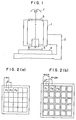
- FIG. 1 is a view used to explain the construction of the prior art device.
- a lens barrel 1 is securely mounted on a stand 2 and a main table 4 upon which is mounted a mask 3 is disposed below the stand 2.
- An original 5 is disposed at the upper end of the lens barrel 1 while a projection lens 6 is mounted at the lower end thereof.
- a light source 7 which is disposed upwardly of the original 5
- the pattern or image on the original 5 is focused through the projection lens 6 over the mask 3.
- Fig. 2 shows a top view of a mask prepared by the device as shown in Fig. 1.
- the original 5 is magnified by five or ten times (this magnification ratio is fixed) and is, in turn, reduced through the projection lens 6 to 1/5 or 1/10 (the reduction ratio is also fixed).
- the reduced image is focused upon a predetermined portion (for instance at P 1 in Fig. 2(a)) of the mask 3. Every time when the image is focused, the main table 4 is stepped .(by a distance a in Fig. 2(a)), whereby patterns are successively transferred. (For instance, the patterns are transferred in the order of P 1 , P 2 , P 3 and so on in Fig. 2(a)).
- the process for manufacture of semiconductor devices includes a heat treatment step so that thermal deformations and shrinkage of wafers result.
- the position and size of a pattern transferred on a wafer are deviated from a desired position and a desired size.
- this "deviation" is very small so that the size of one pattern; that is, the pattern transfer reduction is not changed, but the positions where the patterns are focused; that is, the step is varied in response to the enlargement or reduction of the wafer.
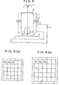
- Fig. 3 is a view used to explain the construction of the first embodiment and same reference numerals are used to designate similar parts throughout the figures.
- a control mechanism 8 is interposed between the upper and lower halves of the lens barrel 1 so that the length of-the lens barrel 1 can be varied and consequently the reduction can be finely adjusted.
- the length of the lens barrel remains unchanged because if the length is varied, the characteristics of the high resolving power lens are adversely affected, but according to the experiments conducted by the inventors it is confirmed that no adverse effect will occur even when the length of the lens barrel is varied by 0.1%.
- the control mechanism 8 may-be a piezoelectric element which changes its thickness when applied with a voltage or a motor and cam mechanism. By changing the length of the lens barrel, the size of a pattern focused on the mask 3 mounted on the main table 4 is varied or adjusted.
- Fig. 4 shows a top view of a mask prepared by the device as shown in Fig. 3.
- the patterns are transferred on the mask 3 as shown in Fig. 4(a).
- the mask 3 is subjected to a heat treatment, it is deformed.
- the rate of shrinkage due to heat treatment is previously obtained so that in response to the rate of shrinkage the rate of reduction is varied by increasing or decreasing the length of the lens barrel 1 by the control mechanism 8.
- the main table 4 and hence the mask 3 are successively stepped as indicated by P 1 , P 2' P 3 and so on. Therefore, the patterns whose "deviations" are minimized can be obtained as shown in Fig. 4(b).
- the position of the projection lens or the original may be varied.
- a zoom lens may be used as a projection lens.
- a second embodiment of a pattern transfer device in accordance with the present invention is shown in Fig. 5.
- a lens barrel 1 is mounted on a stand 2 and a main table 4 upon which is mounted a semiconductor wafer 3 is disposed below the stand 2.
- An original 5 is mounted at the lens barrel 1 while the projection lens 6 is mounted at the lower end of the lens barrel 1.
- a light source 7 is disposed upwardly of the original 5 and a movable mirror 11 is interposed between the original 5 and the light source 7 so that the pattern on the semiconductor wafer 3 may be directed toward a pattern position detector 10.
- a laser interferometer 9 is mounted on the main table 4 so that the position may be detected.
- the control mechanism 8 for making the fine adjustment of the rate of reduction is interposed between the upper and lower halves of the lens barrel 1 so that the length of the lens barrel 1 can be varied.
- the control mechanism 8 may be a piezoelectric element or a motor and cam link as described before.
- the mode of operation will be described.
- the movable mirror 11 is moved out of the optical path from the light source 7 to the original 5 and a pattern P is transferred. That is, the light is projected from the light source 7 to the original 5 so that a reduced pattern is focused on the semiconductor wafer 3 through the projection lens 6.
- the main table 4 is stepped by a distance A and another pattern P is transferred on the semiconductor wafer 3.
- the semiconductor wafer 3 is subjected to a heat treatment step, it is expanded so that a pattern P is enlarged as indicated at (b) in Fig. 6. As a result, the step is increased from A to A + AA. Thereafter a reduced pattern Q is superimposed on the pattern P.
- the movable mirror 11 is moved to the position shown in Fig. 5 so that the pattern transferred on the semiconductor wafer 3 is received or detected by the pattern position detector 10.
- the pattern position detector 10 detects the alignment mark a of the pattern P so that the expanded step A + AA can be detected.
- An extremely small "deviation" AA can be detected by the high precision laser interferometer 9 mounted on the main table 4.
- the transfer reduction of a pattern Q is computed by a control system (not shown).
- the reduction ratio N A + AA of the pattern Q can be obtained from the following equation: where N A is the reduction ratio when the step is A.
- the control mechanism 8 is so operated that the length of the lens barrel 1 is varied and consequently the transfer reduction ratio becomes N A + ⁇ A.
- the movable mirror 11 is moved out of the optical path from the light source 7 to the original 5 and the pattern Q is transferred at the reduction ratio of N A + AA.
- the next pattern Q is transferred in a manner substantially similar to that described above. That is, the step is detected from the alignment marks a of the pattern P and in response to the detected step, the reduction ratio is corrected and then the pattern Q is transferred. In like manner, the patterns Q are successively transferred as shown in Fig. 6(c).
- the patterns may be transferred by minimum misalignment or misregistration.
- the reduction ratio' is varied so that the correct alignment between the patterns P and Q can be ensured even when the semiconductor wafer is locally deformed.
- the transfer reduction ratio is varied every time when a pattern is transferred, but it is to be understood that the steps between typical points on the semiconductor wafer are measured and the average step is obtained so that the reduction ratio can be determined in response .to the average step.
- a pattern may be transferred not only on the surface of a semiconductor wafer but also on a semiconductor mask or the like.
- a prior art device and method for transferring patterns over the surface of a photomask or a semiconductor wafer by the step-and-repeat procedure and by reducing the original pattern is provided with a reduction control means for making the fine adjustment of the reduction so that the size of each pattern can be corrected. Therefore even when a wafer is deformed or shrinked due to heat treatment, not only the step can be corrected but also the size of a pattern can be adjusted so that the misalignment between the patterns can be reduced to a minimum. For instance, if a pattern consisting of 10 xlO elements (patterns) is enlarged by 1. micrometer per 100 millimeter, each element (pattern) is corrected by 0.1 micrometer per 10 millimeter. Then, the most influential cause of the primary misalignment between the patterns can be removed.
- each pattern transfer device has its own temperature so that.it has been considered that it is impossible to transfer patterns on a wafer or the like without any misalignment or misregistration with different pattern transfer devices.
- patterns can be transferred without any misalignment or misregistration with a plurality of pattern transfer devices.
Abstract
Description
- The present invention relates to a step-and-repeat pattern transfer device and method for preparing masks or drawing a pattern directly over the surface of a semiconductor wafer.
- According to a step-and-repeat pattern transfer method, an original image is focused over an object through a high resolving power lens so as to prepare photomasks or draw patterns over the surfaces of semiconductor wafers.
- In this case, due to the thermal treatment or the like, the sizes of a semiconductor wafer vary, but the reduction of a high resolving power lens cannot be varied.
- Therefore, there has been employed a method for varying the distance over which is stepped a focused image or cooling an object so as to reduce its size. In view of a time factor, the former is more practical, but accurate corrections cannot be made.
- The present invention was made to overcome the above and other problems encountered in the prior art step-and-repeat pattern transfer devices and methods and has for its object to provide a device and method for manufacture of semiconductor devices in which alignment or registration between patterns transferred over the surface of a wafer or the like by the step-and-repeat procedure can be improved and deviations of a pattern can be reduced to a minimum.
- To the above and other ends, the present invention provides a device and method for manufacture of semiconductor devices in which a prior art device and method for reducing and focusing an original image by a step-and-repeat procedure so as to prepare a photomask or draw a pattern over the surface of a semiconductor device is provided with a reduction ratio control means for making the fine adjustment of the reduction ratio of an original image so that the sizes of each pattern can be.corrected.
-
- Fig. 1 is a view used to explain the construction of a prior art device;
- Fig. 2 is a top view of a mask prepared by the device as shown in Fig. 1;
- Fig. 3 is a view used to explain the construction of a first embodiment of the present invention;
- Fig. 4 is a top view of a mask prepared by the device as shown in Fig. 3;
- Fig. 5 shows a second embodiment of a pattern transfer device in accordance with the present invention; and
- Figs. 6(a), (b) and (c) are top views of semiconductor wafers upon which are transferred patterns by the device as shown in Fig. 5.
- Prior to the description of the preferred embodi-. ments of the present invention, a prior art device will be described with reference to Figs. 1 and 2.
- A prior art step-and-repeat device and method will be described with reference to Figs. 1 and 2. Fig. 1 is a view used to explain the construction of the prior art device. A
lens barrel 1 is securely mounted on astand 2 and a main table 4 upon which is mounted amask 3 is disposed below thestand 2. An original 5 is disposed at the upper end of thelens barrel 1 while aprojection lens 6 is mounted at the lower end thereof. When the light is projected toward the original 5 from alight source 7 which is disposed upwardly of the original 5, the pattern or image on the original 5 is focused through theprojection lens 6 over themask 3. - Fig. 2 shows a top view of a mask prepared by the device as shown in Fig. 1. The original 5 is magnified by five or ten times (this magnification ratio is fixed) and is, in turn, reduced through the
projection lens 6 to 1/5 or 1/10 (the reduction ratio is also fixed). The reduced image is focused upon a predetermined portion (for instance at P1 in Fig. 2(a)) of themask 3. Every time when the image is focused, the main table 4 is stepped .(by a distance a in Fig. 2(a)), whereby patterns are successively transferred. (For instance, the patterns are transferred in the order of P1, P2, P3 and so on in Fig. 2(a)). - The process for manufacture of semiconductor devices includes a heat treatment step so that thermal deformations and shrinkage of wafers result. As a result, the position and size of a pattern transferred on a wafer are deviated from a desired position and a desired size. In the past, this "deviation" is very small so that the size of one pattern; that is, the pattern transfer reduction is not changed, but the positions where the patterns are focused; that is, the step is varied in response to the enlargement or reduction of the wafer.
- This will be described with reference to Fig. 2. It is assumed that the patterns are transferred by the step-and-repeat reduction as shown in Fig. 2(a) and that because of heat treatment, the
mask 3 is . deformed as shown in Fig. 2(b). Then as indicated by the broken lines, each pattern with a side a changes to a pattern with a side a + Aa. Therefore.in the next step for transferring a pattern by the step-and-repeat procedure, the step a is changed to the step a + Aa. Thus the patterns are transferred in the order of P1. P2' P3 and so on as shown by the solid lines in Fig. 2(b). - When the "deviations" of patterns are corrected only by changing the step without changing the size of the pattern, all the patterns are not same in size so that the problems of characteristics and performances of the semiconductor devices result. These problems are very'serious especially in the case of the manufacture of very large scale integration systems.
- A first embodiment of the present invention will be described with reference to Figs. 3 and 4. Fig. 3 is a view used to explain the construction of the first embodiment and same reference numerals are used to designate similar parts throughout the figures. A
control mechanism 8 is interposed between the upper and lower halves of thelens barrel 1 so that the length of-thelens barrel 1 can be varied and consequently the reduction can be finely adjusted. According to the prior art, the length of the lens barrel remains unchanged because if the length is varied, the characteristics of the high resolving power lens are adversely affected, but according to the experiments conducted by the inventors it is confirmed that no adverse effect will occur even when the length of the lens barrel is varied by 0.1%. Thecontrol mechanism 8 may-be a piezoelectric element which changes its thickness when applied with a voltage or a motor and cam mechanism. By changing the length of the lens barrel, the size of a pattern focused on themask 3 mounted on the main table 4 is varied or adjusted. - Fig. 4 shows a top view of a mask prepared by the device as shown in Fig. 3. First, by the -step-and-repeat reduction procedure, the patterns are transferred on the
mask 3 as shown in Fig. 4(a). Next when themask 3 is subjected to a heat treatment, it is deformed. The rate of shrinkage due to heat treatment is previously obtained so that in response to the rate of shrinkage the rate of reduction is varied by increasing or decreasing the length of thelens barrel 1 by thecontrol mechanism 8. Every time when one pattern is transferred, the main table 4 and hence themask 3 are successively stepped as indicated by P1, P2' P3 and so on. Therefore, the patterns whose "deviations" are minimized can be obtained as shown in Fig. 4(b). - In order to vary the rate of reduction in the case of pattern transfer, the position of the projection lens or the original may be varied. Alternatively, a zoom lens may be used as a projection lens.
- A second embodiment of a pattern transfer device in accordance with the present invention is shown in Fig. 5. A
lens barrel 1 is mounted on astand 2 and a main table 4 upon which is mounted asemiconductor wafer 3 is disposed below thestand 2. An original 5 is mounted at thelens barrel 1 while theprojection lens 6 is mounted at the lower end of thelens barrel 1. Alight source 7 is disposed upwardly of the original 5 and a movable mirror 11 is interposed between the original 5 and thelight source 7 so that the pattern on thesemiconductor wafer 3 may be directed toward apattern position detector 10. A laser interferometer 9 is mounted on the main table 4 so that the position may be detected. Thecontrol mechanism 8 for making the fine adjustment of the rate of reduction is interposed between the upper and lower halves of thelens barrel 1 so that the length of thelens barrel 1 can be varied. Thecontrol mechanism 8 may be a piezoelectric element or a motor and cam link as described before. - Next referring to Fig. 6, the mode of operation will be described. First the movable mirror 11 is moved out of the optical path from the
light source 7 to the original 5 and a pattern P is transferred. That is, the light is projected from thelight source 7 to the original 5 so that a reduced pattern is focused on thesemiconductor wafer 3 through theprojection lens 6. The main table 4 is stepped by a distance A and another pattern P is transferred on thesemiconductor wafer 3. When thesemiconductor wafer 3 is subjected to a heat treatment step, it is expanded so that a pattern P is enlarged as indicated at (b) in Fig. 6. As a result, the step is increased from A to A + AA. Thereafter a reduced pattern Q is superimposed on the pattern P. First, the movable mirror 11 is moved to the position shown in Fig. 5 so that the pattern transferred on thesemiconductor wafer 3 is received or detected by thepattern position detector 10. Thepattern position detector 10 detects the alignment mark a of the pattern P so that the expanded step A + AA can be detected. An extremely small "deviation" AA can be detected by the high precision laser interferometer 9 mounted on the main table 4. Thereafter, the transfer reduction of a pattern Q is computed by a control system (not shown). The reduction ratio NA + AA of the pattern Q can be obtained from the following equation:
control mechanism 8 is so operated that the length of thelens barrel 1 is varied and consequently the transfer reduction ratio becomes NA + ΔA. Thereafter the movable mirror 11 is moved out of the optical path from thelight source 7 to the original 5 and the pattern Q is transferred at the reduction ratio of NA + AA. The next pattern Q is transferred in a manner substantially similar to that described above. That is, the step is detected from the alignment marks a of the pattern P and in response to the detected step, the reduction ratio is corrected and then the pattern Q is transferred. In like manner, the patterns Q are successively transferred as shown in Fig. 6(c). - According to the second embodiment, even when the semiconductor wafer is expanded or shrinked, the patterns may be transferred by minimum misalignment or misregistration. Especially, according to the second embodiment, after the transferred pattern has been measured, the reduction ratio'is varied so that the correct alignment between the patterns P and Q can be ensured even when the semiconductor wafer is locally deformed.
- In the first embodiment, the transfer reduction ratio is varied every time when a pattern is transferred, but it is to be understood that the steps between typical points on the semiconductor wafer are measured and the average step is obtained so that the reduction ratio can be determined in response .to the average step.
- It is to be understood that various modifications can be effected within the scope of.the present invention and that the present invention is not limited to the
control mechanism 8, the laser interferometer 9 and thepattern position detector 10 described above. Furthermore a pattern may be transferred not only on the surface of a semiconductor wafer but also on a semiconductor mask or the like. - As described above, according to the present invention a prior art device and method for transferring patterns over the surface of a photomask or a semiconductor wafer by the step-and-repeat procedure and by reducing the original pattern is provided with a reduction control means for making the fine adjustment of the reduction so that the size of each pattern can be corrected. Therefore even when a wafer is deformed or shrinked due to heat treatment, not only the step can be corrected but also the size of a pattern can be adjusted so that the misalignment between the patterns can be reduced to a minimum. For instance, if a pattern consisting of 10 xlO elements (patterns) is enlarged by 1. micrometer per 100 millimeter, each element (pattern) is corrected by 0.1 micrometer per 10 millimeter. Then, the most influential cause of the primary misalignment between the patterns can be removed.
- There is a one-to-one pattern drawing device in which the reduction is finely adjusted in order to remove the inherent errors. As a result, the reduction cannot be varied in response to the external inputs, the shrinkage of a wafer and so on so that the device cannot obtain the effect that the misalignment between the patterns drawn by the step-and-repeat procedure can be eliminated as the present invention. Each pattern transfer device has its own temperature so that.it has been considered that it is impossible to transfer patterns on a wafer or the like without any misalignment or misregistration with different pattern transfer devices. However, according to the present invention, patterns can be transferred without any misalignment or misregistration with a plurality of pattern transfer devices.
Claims (9)
Applications Claiming Priority (2)
| Application Number | Priority Date | Filing Date | Title |
|---|---|---|---|
| JP22511/83 | 1983-02-14 | ||
| JP58022511A JPS59150424A (en) | 1983-02-14 | 1983-02-14 | Apparatus and method for manufacturing semiconductor device |
Publications (3)
| Publication Number | Publication Date |
|---|---|
| EP0116940A2 true EP0116940A2 (en) | 1984-08-29 |
| EP0116940A3 EP0116940A3 (en) | 1985-01-30 |
| EP0116940B1 EP0116940B1 (en) | 1988-04-20 |
Family
ID=12084781
Family Applications (1)
| Application Number | Title | Priority Date | Filing Date |
|---|---|---|---|
| EP84101498A Expired EP0116940B1 (en) | 1983-02-14 | 1984-02-14 | Pattern transfer device and method |
Country Status (4)
| Country | Link |
|---|---|
| US (1) | US4577945A (en) |
| EP (1) | EP0116940B1 (en) |
| JP (1) | JPS59150424A (en) |
| DE (1) | DE3470611D1 (en) |
Cited By (2)
| Publication number | Priority date | Publication date | Assignee | Title |
|---|---|---|---|---|
| US4737823A (en) * | 1986-06-16 | 1988-04-12 | U.S. Philips Corporation | Opto-lithographic device comprising a displaceable lens system and method of controlling the imaging properties of lens system in such a device |
| EP0531102A1 (en) * | 1991-09-04 | 1993-03-10 | Canon Kabushiki Kaisha | Aligner and exposure method for manufacturing semiconductor device |
Families Citing this family (4)
| Publication number | Priority date | Publication date | Assignee | Title |
|---|---|---|---|---|
| JPH0722101B2 (en) * | 1985-08-29 | 1995-03-08 | 株式会社ニコン | Windshield for projection type exposure equipment |
| ATE63008T1 (en) * | 1986-09-05 | 1991-05-15 | Staude Foto Chemie Eva | DEVICE AND METHOD FOR FILMING DOCUMENTS. |
| JPS63164212A (en) * | 1986-12-26 | 1988-07-07 | Hitachi Ltd | Reduction stepper |
| JP5134767B2 (en) * | 2005-04-19 | 2013-01-30 | 株式会社オーク製作所 | Drawing apparatus having drawing data correction function |
Citations (2)
| Publication number | Priority date | Publication date | Assignee | Title |
|---|---|---|---|---|
| FR2388300A1 (en) * | 1977-04-20 | 1978-11-17 | Thomson Csf | OPTICAL PATTERN PROJECTION DEVICE INCLUDING FOCUS OF FOCUS AT CONSTANT GROWTH |
| EP0017044A2 (en) * | 1979-04-02 | 1980-10-15 | Eaton-Optimetrix Inc. | A system for positioning a utilization device |
Family Cites Families (6)
| Publication number | Priority date | Publication date | Assignee | Title |
|---|---|---|---|---|
| US3744902A (en) * | 1968-10-23 | 1973-07-10 | Siemens Ag | Device for producing a photo-varnish mask |
| US4108941A (en) * | 1976-04-26 | 1978-08-22 | Dolco Packaging Corporation | Shear molding of reinforced latch |
| US4190325A (en) * | 1977-12-02 | 1980-02-26 | Ford Motor Company | Thermal compensator assembly |
| US4383757A (en) * | 1979-04-02 | 1983-05-17 | Optimetrix Corporation | Optical focusing system |
| US4414749A (en) * | 1979-07-02 | 1983-11-15 | Optimetrix Corporation | Alignment and exposure system with an indicium of an axis of motion of the system |
| JPS57192929A (en) * | 1981-05-25 | 1982-11-27 | Hitachi Ltd | Projector provided with automatic focusing function |
-
1983
- 1983-02-14 JP JP58022511A patent/JPS59150424A/en active Pending
-
1984
- 1984-02-10 US US06/578,815 patent/US4577945A/en not_active Expired - Lifetime
- 1984-02-14 DE DE8484101498T patent/DE3470611D1/en not_active Expired
- 1984-02-14 EP EP84101498A patent/EP0116940B1/en not_active Expired
Patent Citations (2)
| Publication number | Priority date | Publication date | Assignee | Title |
|---|---|---|---|---|
| FR2388300A1 (en) * | 1977-04-20 | 1978-11-17 | Thomson Csf | OPTICAL PATTERN PROJECTION DEVICE INCLUDING FOCUS OF FOCUS AT CONSTANT GROWTH |
| EP0017044A2 (en) * | 1979-04-02 | 1980-10-15 | Eaton-Optimetrix Inc. | A system for positioning a utilization device |
Cited By (3)
| Publication number | Priority date | Publication date | Assignee | Title |
|---|---|---|---|---|
| US4737823A (en) * | 1986-06-16 | 1988-04-12 | U.S. Philips Corporation | Opto-lithographic device comprising a displaceable lens system and method of controlling the imaging properties of lens system in such a device |
| EP0531102A1 (en) * | 1991-09-04 | 1993-03-10 | Canon Kabushiki Kaisha | Aligner and exposure method for manufacturing semiconductor device |
| US5270771A (en) * | 1991-09-04 | 1993-12-14 | Canon Kabushiki Kaisha | Aligner and exposure method for manufacturing semiconductor device |
Also Published As
| Publication number | Publication date |
|---|---|
| US4577945A (en) | 1986-03-25 |
| EP0116940A3 (en) | 1985-01-30 |
| JPS59150424A (en) | 1984-08-28 |
| EP0116940B1 (en) | 1988-04-20 |
| DE3470611D1 (en) | 1988-05-26 |
Similar Documents
| Publication | Publication Date | Title |
|---|---|---|
| US4811055A (en) | Projection exposure apparatus | |
| US4734746A (en) | Exposure method and system for photolithography | |
| US4708466A (en) | Exposure apparatus | |
| US6014455A (en) | Projection exposure apparatus and device manufacturing method | |
| US4488806A (en) | Shot arranging method in a divisional printing apparatus | |
| EP0116940B1 (en) | Pattern transfer device and method | |
| JPH10133150A (en) | Diffraction optical device and aligner using the same | |
| US6847432B2 (en) | Alignment system and projection exposure apparatus | |
| JP2914315B2 (en) | Scanning reduction projection exposure apparatus and distortion measuring method | |
| US6859265B2 (en) | Stage device, method of controlling same, and exposure apparatus | |
| JP2000195784A (en) | Aligner manufacture of device | |
| US6256085B1 (en) | Exposure apparatus | |
| JPS60138926A (en) | Pattern transfer device | |
| US20070072128A1 (en) | Method of manufacturing an integrated circuit to obtain uniform exposure in a photolithographic process | |
| JPH1174190A (en) | X-ray aligner | |
| JP3550034B2 (en) | Exposure method and exposure apparatus | |
| JPH0550849B2 (en) | ||
| KR100390818B1 (en) | Method for forming uniform patterns of semiconductor device | |
| JP2876406B2 (en) | Exposure apparatus and exposure method | |
| KR0144412B1 (en) | Lens reduction ratio adjustment method of exposure apparatus | |
| JP2001160533A (en) | Projection aligner and device producing method | |
| Nagaswami | In-plane distortion in silicon wafers induced by a submicron CMOS process | |
| JPS6269618A (en) | Optical device for projection | |
| JP2005109333A (en) | Device for manufacturing semiconductor and method for manufacturing device | |
| JPH10125578A (en) | Exposure method |
Legal Events
| Date | Code | Title | Description |
|---|---|---|---|
| PUAI | Public reference made under article 153(3) epc to a published international application that has entered the european phase |
Free format text: ORIGINAL CODE: 0009012 |
|
| 17P | Request for examination filed |
Effective date: 19840214 |
|
| AK | Designated contracting states |
Designated state(s): DE FR GB IT |
|
| PUAL | Search report despatched |
Free format text: ORIGINAL CODE: 0009013 |
|
| AK | Designated contracting states |
Designated state(s): DE FR GB IT |
|
| 17Q | First examination report despatched |
Effective date: 19860610 |
|
| GRAA | (expected) grant |
Free format text: ORIGINAL CODE: 0009210 |
|
| AK | Designated contracting states |
Kind code of ref document: B1 Designated state(s): DE FR GB IT |
|
| REF | Corresponds to: |
Ref document number: 3470611 Country of ref document: DE Date of ref document: 19880526 |
|
| ET | Fr: translation filed | ||
| ITF | It: translation for a ep patent filed |
Owner name: SOCIETA' ITALIANA BREVETTI S.P.A. |
|
| PLBE | No opposition filed within time limit |
Free format text: ORIGINAL CODE: 0009261 |
|
| STAA | Information on the status of an ep patent application or granted ep patent |
Free format text: STATUS: NO OPPOSITION FILED WITHIN TIME LIMIT |
|
| 26N | No opposition filed | ||
| ITTA | It: last paid annual fee | ||
| PGFP | Annual fee paid to national office [announced via postgrant information from national office to epo] |
Ref country code: GB Payment date: 19970205 Year of fee payment: 14 |
|
| PGFP | Annual fee paid to national office [announced via postgrant information from national office to epo] |
Ref country code: FR Payment date: 19970211 Year of fee payment: 14 |
|
| PGFP | Annual fee paid to national office [announced via postgrant information from national office to epo] |
Ref country code: DE Payment date: 19970221 Year of fee payment: 14 |
|
| PG25 | Lapsed in a contracting state [announced via postgrant information from national office to epo] |
Ref country code: GB Free format text: LAPSE BECAUSE OF NON-PAYMENT OF DUE FEES Effective date: 19980214 |
|
| PG25 | Lapsed in a contracting state [announced via postgrant information from national office to epo] |
Ref country code: FR Free format text: THE PATENT HAS BEEN ANNULLED BY A DECISION OF A NATIONAL AUTHORITY Effective date: 19980228 |
|
| GBPC | Gb: european patent ceased through non-payment of renewal fee |
Effective date: 19980214 |
|
| PG25 | Lapsed in a contracting state [announced via postgrant information from national office to epo] |
Ref country code: DE Free format text: LAPSE BECAUSE OF NON-PAYMENT OF DUE FEES Effective date: 19981103 |
|
| REG | Reference to a national code |
Ref country code: FR Ref legal event code: ST |