EP0136178A2 - Automatic memory board reconfiguration - Google Patents
Automatic memory board reconfiguration Download PDFInfo
- Publication number
- EP0136178A2 EP0136178A2 EP84306590A EP84306590A EP0136178A2 EP 0136178 A2 EP0136178 A2 EP 0136178A2 EP 84306590 A EP84306590 A EP 84306590A EP 84306590 A EP84306590 A EP 84306590A EP 0136178 A2 EP0136178 A2 EP 0136178A2
- Authority
- EP
- European Patent Office
- Prior art keywords
- memory
- board
- address
- boards
- configuration
- Prior art date
- Legal status (The legal status is an assumption and is not a legal conclusion. Google has not performed a legal analysis and makes no representation as to the accuracy of the status listed.)
- Withdrawn
Links
Images


Classifications
-
- G—PHYSICS
- G06—COMPUTING; CALCULATING OR COUNTING
- G06F—ELECTRIC DIGITAL DATA PROCESSING
- G06F12/00—Accessing, addressing or allocating within memory systems or architectures
- G06F12/02—Addressing or allocation; Relocation
-
- G—PHYSICS
- G06—COMPUTING; CALCULATING OR COUNTING
- G06F—ELECTRIC DIGITAL DATA PROCESSING
- G06F12/00—Accessing, addressing or allocating within memory systems or architectures
- G06F12/02—Addressing or allocation; Relocation
- G06F12/06—Addressing a physical block of locations, e.g. base addressing, module addressing, memory dedication
- G06F12/0646—Configuration or reconfiguration
- G06F12/0653—Configuration or reconfiguration with centralised address assignment
- G06F12/0661—Configuration or reconfiguration with centralised address assignment and decentralised selection
Definitions
- the present invention relates to automatic configuration of computer memory on startup. More specifically, it relates to the use of stored configuration data from each memory board to automatically assign memory boards to contiguous sectors of memory, without human operator intervention.
- Computer memory is generally structured as a linear array of words; each word is assigned a single address and contains a fixed amount (e.g., 32 bits) of data. Memory chips store the data and respond to each address with that word's data. Several memory chips are collected on a single circuit board, and several circuit boards are used to make up the address space of the computer.
- Each circuit board is assigned to a sector of memory and makes up only part of the computer's entire memory address space. It must be configured to respond to addresses in that sector of memory, and to no other addresses.
- the circuit board is designed to access the proper group of its memory chips when responding to a memory request.
- Circuit boards and the memory chips they contain are fallible pieces of electronic equipment; they must therefore be tested for failures. Generally this is done when the memory is first configured. Boards with errors must not be included in the memory address space, since this might result in erroneous data reads or dita writes.
- Each memory circuit board is typically connected to the computer's memory address bus.
- the memory address bus is used to transmit the processor's memory access requests to the memory.
- Each board examines the asserted memory address and determines if it is being accessed; it responds if it is. This is normally done by comparing the high-order bits of the asserted address with the memory board's allocated position in memory address space.
- One method which is often employed in the prior art to configure the memory address space is to set manual switches or to connect jumpers on the circuit board to indicate its position in memory address space.
- the high-order bits of the asserted address are directly compared with these switch values, and the memory responds when they are equal.
- Each memory circuit board for use with the present invention contains a nonvolatile memory and a configuration register. These are used to record the board's size, default address space, and its actually assigned address space.
- a microprocessor reads the size and default address space from each board and tests the information for errors. It then uses a general process to assign memory boards to address spaces which assures that a continuous unbroken, and non-overlapping array of memory addresses is available to the pr " essor. Next, it stores each board's address space assignment in th board's configuration register. This information is later used by th memory boards during operation of the system to respond to memory accesses requested by the processor.
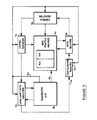
- One or more memory boards 10 are connected to the computer's memory address bus 12. This allows memory access to those boards by the CPU 14.
- the boards are physically placed in a connector backplane (not illustrated). In contrast with the requirement of contiguous, sorted board placement which is found in the prior art, physical order does not matter, and so the boards may be placed arbitrarily.
- nonvolatile memory 16 which records the memory size and its default address range.
- nonvolatile memory 16 is a nonvolatile RAM (NOVRAM).
- NOVRAM nonvolatile RAM
- those skilled in the art will recognize that other forms of nonvolatile memory, such as electrically erasable read only memory would be used, or that CMOS RAMs or registers with battery backup could be employed.
- nonvolatile memory 16 are read by a diagnostic microprocessor 18 so it may assign boards to their actual address ranges according to the memory configuration process although the main processor or any processor in the system could be used to perform this task.
- the Z-80 microprocessor from Zilog, Inc., is suitable for this purpose.
- Configuration register 20 may be one of numerous data processing registers known in the art, although in the preferred embodiment it is a serial and parallel access register.
- the configuration code is kept in a location in nonvolatile memory 16 and will also be written into the nonvolatile memory 16 if an update is required.
- configuration register 20 is five bits wide.
- the five bits of the configuration register 20 include three bits of address range (the three high-order bits of the base address for this memory board's address slot) and two bits which indicate the memory board size.
- each memory board may be physically one or two million bytes of memory.
- Each bit of the size value, when set, indicates that one of the two halves of the memory board is present.
- the microprocessor 18 does not use the memory bus 12 to read and write the configuration register 20 3 nonvolatile memory 16. Instead it uses a secondary acceus path : , employing "edge triggered scan design.” Scan design is well known the art; it involves connecting registers together in a large sift-register loop and using repeated bit shifting to read or to write the contents of any register. This access path is more fully explained below with reference to figure 3. Those skilled in the art will realize that access to configuration register 20 and nonvolatile memory 16 could easily be accomplished across the normal parallel memory bus 12 or by other forms of secondary access, such as a parallel maintenance bus. A signal or code appearing on one or more address or control lines could condition these elements (configuration register 20 and nonvolatile memory 16) to read or write data.
- each memory board 10 When the memory address space is configured, each memory board 10 will know its assigned address space by the contents of its configuration register 20. Each memory access is performed by having the CPU 14 assert a memory address onto the memory address bus 12. Each memory board 10 examines this address and compares it with its assigned address space, as is more fully explained with reference to figure 4. If the asserted address is within the address range of the memory board, an access occurs to the memory array shown diagramatically at 24.
- the configuration process is invoked during the power-on sequence when the system is started, but those skilled in the art will readily see that it can be invoked at most any time under software control, i.e., reconfiguration could be invoked after a memory access failure.
- the diagnostic microprocessor 18 executes the configuration process under the control of its local control store 26 and uses the local buffer store 28 in the preferred embodiment although it may use control store and buffer space used by another processor.
- the microprocessor 18 examines each memory slot for the presence of a memory board 10. It does this by testing the secondary access path to each memory slot. Memory slots which do not pass this test are presumed not to contain functioning memory boards. Only boards which are present and functioning are used to configure the memory address space.
- This test is performed as follows: First, a pattern or all ones followed by one of all zeros is loaded and read back from each slots shift string. Those slots not returning the input data are failed immediately. For the remaining slots, a test pattern consisting of series of ones with the least significant bit set to a zero is created and loaded into the first slot's shift string. The zero is left shifted in the pattern and the next slot's string is loaded. This procedure is repeated until all of the slots' shift strings are loaded. The size of the test pattern in bits corresponds to the number of shift strings to be accessed. Once loaded, all the patterns are read back and verified.
- Any pattern mismatch is resolved to a failing slot using the following two simple rules: If the pattern returned by the slot's shift string contains a one in the bit position where a zero was stored, then the slot accessed is also responding to the selection of another slot. If the pattern returned by the slot's shift string contains a zero in the bit position where a one was stored, then another slot is also responding to the one being accessed. Any extra zeros found can be resolved to a failing slot by the direct correspondence hetween the bit position of the extra zero and the slot having selection problems.
- the minimum size of the test pattern must be four bits.
- the unique test patterns are oaded into each slot's string so that the four strings contain the ollowing patterns: 1110, 1101, 1011, 0111.
- the patterns are thef read back and verified to contain the patterns above. The following are two error cases and how they are handled using the previously defined rules:
- the test would flag the first bad string found. Once the first error was corrected, the second bad slot would be flagged.
- microprocessor 18 reads the contents of each board's nonvolatile memory 16. It records the results in its local buffer memory 28.
- Each nonvolatile memory 16 may also be checked for erroneous data.
- the nonvolatile memory 16 on a given memory board 10 may contain, as part of it's information, a unique serial number for the board. To use this information to test selection, the serial number and it's complement along with a copy of the two values may be contained in the nonvolatile memory. When checking for selection, the serial number and its complement are read and the two values verified against each other. If a miscompare occurs, the copy of the serial number and its complement are read and verified. The same miscompare occurring in the copy indicates that there are two slots responding to the select. Any other miscompare or no miscompare in the copy indicates that there is a data error in the nonvolatile memory 16. Thus it is possible to use only boards which are error-free to configure the memory address space.
- the microprocessor 10 tests to see if the collection of default address ranges which it has read from the memory boards 10 forms a "feasible" configuration.
- a feasible configuration is one in which the address ranges assigned to the memory boards include the address zero, do not overlap, and collectively form a contiguous range of addresses.. If the configuration is feasible the microprocessor proceeds to step 58 to write out the configuration to the configuration registers; otherwise it executes steps 60, 62 and then 58 to create a new feasible configuration, and write out the configuration to the configuration registers.
- the microprocessor 18 creates a new feasible configuration. In a preferred embodiment, it does this by allocating the larger memory boards to lower positions in the memory address space; this assures that there are no breaks or overlaps in the array of addressable memory words, and reduces the probability of reconfiguration later on.
- the diagnostic microprocessor 18 selects the largest size memory board 10 not yet assigned a memory L if there are several of the same size, it preferably selects the one with the lowest memory slot number.
- the sell ction is somewhat arbitrary and any selection falls within the scope of the present invention.
- it assigns an appropriately sized range of addresses that begins with the lowest unassigned memory address to the memory board.
- it records this assignment in its local buffer memory 28. If there are no more memory boards to assign, the new feasible configuration is fully created. Otherwise, the microprocessor returns to step 60a and continues until a new feasible configuration is in fact fully created.
- the microprocessor 18 rewrites the nonvolatile memory for each memory board to make its default address range equal to its actual address range.. It uses the secondary access path 22 to perform the write in the preferred embodiment. Although in a preferred embodiment it writes to all memory boards from its buffer memory after completing the configuration assignments, microprocessor 18 could also write to each memory board as its assignment is made.
- the nonvolatile memory is only rewritten rarely, because some nonvolatile memories can only be written a small (about 1000) number of times before they fail.
- the microprocessor 18 writes the configuration register for each memory board with its actual address range, using the secondary access path 16 to perform the write. This concludes the memory configuration processes.
- the configuration register 20 along with other registers on each memory board 10 are linked into a large serial shift-register assembly which allows them to be serially accessed.
- Serial shift path 30 is shown in dashed Lines.
- the diagnostic microprocessor 18 asserts a control signal on line 32 to all these registers which places the registers in serial shift mode.
- the microprocessor 18 When it wishes to read a particular register, the microprocessor 18 shifts the data in the shift register assembly the requisite number of bits until the register's contents are present in its local shift byte register 34, it then reads the contents of the local register directly. To write values, it loads its local shift byte register 34 and shifts the data in the shift-register assembly the requisite number of bits until the data byte has reached the desired register.
- the program running in microprocessor 18 has knowledge of the total length of all the registers on the memory board, so it shifts the proper number of bits in every case.
- Nonvolatile memory control register 36 supplies the commands to which the memory responds.
- Nonvolatile memory address register 38 supplies addresses to the memory and nonvolatile memory data register 40 is used to pass data in and out of nonvolatile memory 16.
- a NOVRAM as used in the preferred embodiment, is divided in practice into two parts, a volatile portion 16a and an nonvolatile portion 16b.
- the microprocessor scans values into the NV memory control register 36, the NV memory address register 38, and the NV memory data register 40. It then asserts a control signal to the nonvolatile memory via line 42 which instructs the memory to perform a data transfer.
- the NOVRAM recognizes four control signals: READ, WRITE, STORE, and RECALL.
- READ and WRITE will alter the volatile portion 16a directly.
- the STORE command will alter the nonvolatile portion 16b to be a copy of the volatile superstrate, while the RECALL command will copy the nonvolatile portion to the volatile portion.
- the WRITE and STORE commands are issued together to assure that data written to the nonvolatile memory is not lost.
- nonvolatile memory These described properties of the nonvolatile memory are common to NOVRAMs in the industry and are well known in the art. They are also completely transparent to the user of the invention, as those skilled in the art can readily see. It will be understood that if other types of memory are employed for use as nonvolatile memory 16, the above-described control sequence will be altered accordingly.
- Each memory board 10 contains a PROM 44 which it uses to determine which memory addresses asserted on the memory address bus 12 by the CPU are for that board.
- the five high-order bits of the asserted memory address are placed on the PROM address lines 46.
- Five bits from the configuration register 18 are placed on the address lines 48.
- the PROM 44 responds with a 4-bit vector 50 which tells the memory board which, if any, memory "bank,” or quarter-board, should be accessed.
- PROM 44 is programmed to recognize combinations of code and address that warrant a response. If the 4-bit vector is all zero, the memory board does not respond at all. Otherwise one of the four lines comprising vector 50 will contain a logic one which will enable one bank or quarter the memory array 24.
- a comparator could be used to compare the two sets of five bits and enable the entire memory board.
Abstract
Description
- The present invention relates to automatic configuration of computer memory on startup. More specifically, it relates to the use of stored configuration data from each memory board to automatically assign memory boards to contiguous sectors of memory, without human operator intervention.
- Computer memory is generally structured as a linear array of words; each word is assigned a single address and contains a fixed amount (e.g., 32 bits) of data. Memory chips store the data and respond to each address with that word's data. Several memory chips are collected on a single circuit board, and several circuit boards are used to make up the address space of the computer.
- Each circuit board is assigned to a sector of memory and makes up only part of the computer's entire memory address space. It must be configured to respond to addresses in that sector of memory, and to no other addresses. The circuit board is designed to access the proper group of its memory chips when responding to a memory request.
- Circuit boards and the memory chips they contain are fallible pieces of electronic equipment; they must therefore be tested for failures. Generally this is done when the memory is first configured. Boards with errors must not be included in the memory address space, since this might result in erroneous data reads or dita writes.
- Each memory circuit board is typically connected to the computer's memory address bus. The memory address bus is used to transmit the processor's memory access requests to the memory. Each board examines the asserted memory address and determines if it is being accessed; it responds if it is. This is normally done by comparing the high-order bits of the asserted address with the memory board's allocated position in memory address space.
- One method which is often employed in the prior art to configure the memory address space is to set manual switches or to connect jumpers on the circuit board to indicate its position in memory address space. The high-order bits of the asserted address are directly compared with these switch values, and the memory responds when they are equal.
- Another method which has been employed in the prior art is to use adders to keep a running count of the cumulative amount of memory in the system. Each memory board can use the total amount of space below it to define its address range. See "A High Performance Memory System with Growth Capability," 33:3 HP Journal 15 (March 1982). However, this arrangement requires boards to be assigned to contiguous slots in the backplane according to decreasing size. In addition, there is no way to configure around defective boards.
- While these methods of the prior art accomplish their objective, to allow the use of multiple memory circuit boards in a computer system, they have some drawbacks. Normally, memory boards must be placed in the computer backplace in order of their memory capacity, denser memory boards assigned to lower address slots. Memory configuration must be performed at least in part by hand; it cannot be performed automatically or as part of a dynamic recovery from a machine error. There exists a need to solve these problems and to use an improved memory configuration procedure.
- Therefore, it is an object of the present invention to improve flexibility in configuring memory for computer systems, by reducing the work needed to alter the memory of the system, by removing the requirement for sorted placement of memory boards, and by removing the requirement for human operator intervention.
- It is a second object of the present invention to reduce the number and frequency of errors in memory configuration, by reducing the work needed to alter the memory of the system, and by removing the requirement for human operator intervention.
- It is yet a third object of the present invention to improve the ease and speed of memory configuration, by reducing the work needed to alter the memory of the system, by removing the requirement for sorted placement of memory boards, and by removing the requirement for human operator intervention.
- These and other objects of the present invention will be more clearly understood from an examination of the specification, the drawings, and the accompanying claims.
- Each memory circuit board for use with the present invention contains a nonvolatile memory and a configuration register. These are used to record the board's size, default address space, and its actually assigned address space. A microprocessor reads the size and default address space from each board and tests the information for errors. It then uses a general process to assign memory boards to address spaces which assures that a continuous unbroken, and non-overlapping array of memory addresses is available to the pr "essor. Next, it stores each board's address space assignment in th board's configuration register. This information is later used by th memory boards during operation of the system to respond to memory accesses requested by the processor.
-
- Figure 1 is a block diagram of the system hardware for the invention.
- Figure 2a is a flow chart of the memory configuration process.
- Figure 2b is a flow chart of the feasible configuration creation process.
- Figure 3 is a block diagram of the secondary access path to the configuration register and the nonvolatile memory on the memory board in a preferred embodiment of the invention.
- Figure 4 is a block diagram of the memory board address selection hardware in a preferred embodiment of the present. invention.
- Referring now to Figure 1, the system hardware for the. invention is described.
- One or
more memory boards 10 are connected to the computer'smemory address bus 12. This allows memory access to those boards by theCPU 14. The boards are physically placed in a connector backplane (not illustrated). In contrast with the requirement of contiguous, sorted board placement which is found in the prior art, physical order does not matter, and so the boards may be placed arbitrarily. - Included on each board is a
nonvolatile memory 16, which records the memory size and its default address range. In a preferred embodiment of the present invention,nonvolatile memory 16 is a nonvolatile RAM (NOVRAM). However, given this disclosure, those skilled in the art will recognize that other forms of nonvolatile memory, such as electrically erasable read only memory would be used, or that CMOS RAMs or registers with battery backup could be employed. - In a preferred embodiment, the contents of
nonvolatile memory 16 are read by adiagnostic microprocessor 18 so it may assign boards to their actual address ranges according to the memory configuration process although the main processor or any processor in the system could be used to perform this task. The Z-80 microprocessor, from Zilog, Inc., is suitable for this purpose. - A code which defines the actual address range assigned to each
memory board 10 is written into aconfiguration register 20 located on the board after it has been determined.Configuration register 20 may be one of numerous data processing registers known in the art, although in the preferred embodiment it is a serial and parallel access register. The configuration code is kept in a location innonvolatile memory 16 and will also be written into thenonvolatile memory 16 if an update is required. - In a preferred embodiment,
configuration register 20 is five bits wide. The five bits of theconfiguration register 20 include three bits of address range (the three high-order bits of the base address for this memory board's address slot) and two bits which indicate the memory board size. In the present embodiment, each memory board may be physically one or two million bytes of memory. Each bit of the size value, when set, indicates that one of the two halves of the memory board is present. - In the preferred embodiment, the
microprocessor 18 does not use thememory bus 12 to read and write theconfiguration register 20 3nonvolatile memory 16. Instead it uses a secondary acceus path : , employing "edge triggered scan design." Scan design is well known the art; it involves connecting registers together in a large sift-register loop and using repeated bit shifting to read or to write the contents of any register. This access path is more fully explained below with reference to figure 3. Those skilled in the art will realize that access to configuration register 20 andnonvolatile memory 16 could easily be accomplished across the normalparallel memory bus 12 or by other forms of secondary access, such as a parallel maintenance bus. A signal or code appearing on one or more address or control lines could condition these elements (configuration register 20 and nonvolatile memory 16) to read or write data. - When the memory address space is configured, each
memory board 10 will know its assigned address space by the contents of itsconfiguration register 20. Each memory access is performed by having theCPU 14 assert a memory address onto thememory address bus 12. Eachmemory board 10 examines this address and compares it with its assigned address space, as is more fully explained with reference to figure 4. If the asserted address is within the address range of the memory board, an access occurs to the memory array shown diagramatically at 24. - The configuration process is invoked during the power-on sequence when the system is started, but those skilled in the art will readily see that it can be invoked at most any time under software control, i.e., reconfiguration could be invoked after a memory access failure. The
diagnostic microprocessor 18 executes the configuration process under the control of itslocal control store 26 and uses thelocal buffer store 28 in the preferred embodiment although it may use control store and buffer space used by another processor. - Referring now to figure 2a, the configuration process is described.
- At
step 52, themicroprocessor 18 examines each memory slot for the presence of amemory board 10. It does this by testing the secondary access path to each memory slot. Memory slots which do not pass this test are presumed not to contain functioning memory boards. Only boards which are present and functioning are used to configure the memory address space. - This test is performed as follows: First, a pattern or all ones followed by one of all zeros is loaded and read back from each slots shift string. Those slots not returning the input data are failed immediately. For the remaining slots, a test pattern consisting of series of ones with the least significant bit set to a zero is created and loaded into the first slot's shift string. The zero is left shifted in the pattern and the next slot's string is loaded. This procedure is repeated until all of the slots' shift strings are loaded. The size of the test pattern in bits corresponds to the number of shift strings to be accessed. Once loaded, all the patterns are read back and verified. Any pattern mismatch is resolved to a failing slot using the following two simple rules: If the pattern returned by the slot's shift string contains a one in the bit position where a zero was stored, then the slot accessed is also responding to the selection of another slot. If the pattern returned by the slot's shift string contains a zero in the bit position where a one was stored, then another slot is also responding to the one being accessed. Any extra zeros found can be resolved to a failing slot by the direct correspondence hetween the bit position of the extra zero and the slot having selection problems.
- If, for example, four slots are to be tested, the minimum size of the test pattern must be four bits. The unique test patterns are oaded into each slot's string so that the four strings contain the ollowing patterns: 1110, 1101, 1011, 0111. The patterns are thef read back and verified to contain the patterns above. The following are two error cases and how they are handled using the previously defined rules:
- Suppose that
slot 1 responds to selection of slot 3. The pattern returned whenslot 1 is accessed would be 1011. Since the underlined bit should be a zero but is a one, this indicates thatslot 1 selection is defective. - Further, suppose that both slots 3 and 4 respond to selection of string 3. The pattern returned when slot 3 is accessed would be 0011. Since the bit corresponding to the slot accessed is zero as it should be, the additional zero in the first position indicates slot four has defective selection circuitry.
- In the case of two slots responding to each other's selection, the test would flag the first bad string found. Once the first error was corrected, the second bad slot would be flagged.
- Next, at
step 54,microprocessor 18 reads the contents of each board'snonvolatile memory 16. It records the results in itslocal buffer memory 28. Eachnonvolatile memory 16 may also be checked for erroneous data. Thenonvolatile memory 16 on a givenmemory board 10 may contain, as part of it's information, a unique serial number for the board. To use this information to test selection, the serial number and it's complement along with a copy of the two values may be contained in the nonvolatile memory. When checking for selection, the serial number and its complement are read and the two values verified against each other. If a miscompare occurs, the copy of the serial number and its complement are read and verified. The same miscompare occurring in the copy indicates that there are two slots responding to the select. Any other miscompare or no miscompare in the copy indicates that there is a data error in thenonvolatile memory 16. Thus it is possible to use only boards which are error-free to configure the memory address space. - At
step 56, themicroprocessor 10 tests to see if the collection of default address ranges which it has read from thememory boards 10 forms a "feasible" configuration. A feasible configuration. is one in which the address ranges assigned to the memory boards include the address zero, do not overlap, and collectively form a contiguous range of addresses.. If the configuration is feasible the microprocessor proceeds to step 58 to write out the configuration to the configuration registers; otherwise it executessteps - At
step 60, themicroprocessor 18 creates a new feasible configuration. In a preferred embodiment, it does this by allocating the larger memory boards to lower positions in the memory address space; this assures that there are no breaks or overlaps in the array of addressable memory words, and reduces the probability of reconfiguration later on. - Referring now to figure 2b, the feasible configuration creation process is described in greater detail.
- At
step 60a, thediagnostic microprocessor 18 selects the largestsize memory board 10 not yet assigned a memory L if there are several of the same size, it preferably selects the one with the lowest memory slot number. The sell ction is somewhat arbitrary and any selection falls within the scope of the present invention. Atstep 60b, it assigns an appropriately sized range of addresses that begins with the lowest unassigned memory address to the memory board. Atstep 60c, it records this assignment in itslocal buffer memory 28. If there are no more memory boards to assign, the new feasible configuration is fully created. Otherwise, the microprocessor returns to step 60a and continues until a new feasible configuration is in fact fully created. - At
step 62, themicroprocessor 18 rewrites the nonvolatile memory for each memory board to make its default address range equal to its actual address range.. It uses the secondary access path 22 to perform the write in the preferred embodiment. Although in a preferred embodiment it writes to all memory boards from its buffer memory after completing the configuration assignments,microprocessor 18 could also write to each memory board as its assignment is made. The nonvolatile memory is only rewritten rarely, because some nonvolatile memories can only be written a small (about 1000) number of times before they fail. - At
step 58, themicroprocessor 18 writes the configuration register for each memory board with its actual address range, using thesecondary access path 16 to perform the write. This concludes the memory configuration processes. - Referring now to figure 3, the preferred secondary (scan design) access path is described.
- The
configuration register 20 along with other registers on eachmemory board 10 are linked into a large serial shift-register assembly which allows them to be serially accessed. Serial shift path 30 is shown in dashed Lines. Thediagnostic microprocessor 18 asserts a control signal online 32 to all these registers which places the registers in serial shift mode. - When it wishes to read a particular register, the
microprocessor 18 shifts the data in the shift register assembly the requisite number of bits until the register's contents are present in its localshift byte register 34, it then reads the contents of the local register directly. To write values, it loads its localshift byte register 34 and shifts the data in the shift-register assembly the requisite number of bits until the data byte has reached the desired register. - The program running in
microprocessor 18 has knowledge of the total length of all the registers on the memory board, so it shifts the proper number of bits in every case. - On each
memory board 10, as a means of servicingnonvolatile memory 16, three registers are provided. Nonvolatile memory control register 36 supplies the commands to which the memory responds. Nonvolatilememory address register 38 supplies addresses to the memory and nonvolatile memory data register 40 is used to pass data in and out ofnonvolatile memory 16. - Though the
configuration register 20 is written and read using just this process, the nonvolatile memory may need to be read and written in a more complex manner. A NOVRAM, as used in the preferred embodiment, is divided in practice into two parts, a volatile portion 16a and an nonvolatile portion 16b. To affect the nonvolatile memory, the microprocessor scans values into the NVmemory control register 36, the NVmemory address register 38, and the NV memory data register 40. It then asserts a control signal to the nonvolatile memory vialine 42 which instructs the memory to perform a data transfer. - The NOVRAM recognizes four control signals: READ, WRITE, STORE, and RECALL. READ and WRITE will alter the volatile portion 16a directly. The STORE command will alter the nonvolatile portion 16b to be a copy of the volatile superstrate, while the RECALL command will copy the nonvolatile portion to the volatile portion. In practice, the WRITE and STORE commands are issued together to assure that data written to the nonvolatile memory is not lost.
- These described properties of the nonvolatile memory are common to NOVRAMs in the industry and are well known in the art. They are also completely transparent to the user of the invention, as those skilled in the art can readily see. It will be understood that if other types of memory are employed for use as
nonvolatile memory 16, the above-described control sequence will be altered accordingly. - Referring now to figure 4, the memory board comparator is described.
- Each
memory board 10 contains a PROM 44 which it uses to determine which memory addresses asserted on thememory address bus 12 by the CPU are for that board. The five high-order bits of the asserted memory address are placed on the PROM address lines 46. Five bits from theconfiguration register 18 are placed on the address lines 48. The PROM 44 responds with a 4-bit vector 50 which tells the memory board which, if any, memory "bank," or quarter-board, should be accessed. PROM 44 is programmed to recognize combinations of code and address that warrant a response. If the 4-bit vector is all zero, the memory board does not respond at all. Otherwise one of the fourlines comprising vector 50 will contain a logic one which will enable one bank or quarter thememory array 24. Of course a comparator could be used to compare the two sets of five bits and enable the entire memory board. - Those skilled in the art will recognize that while a preferred embodiment has been disclosed, variations are possible without departing from the intended scope of the present invention.
Claims (1)
Applications Claiming Priority (2)
| Application Number | Priority Date | Filing Date | Title |
|---|---|---|---|
| US53704083A | 1983-09-29 | 1983-09-29 | |
| US537040 | 1983-09-29 |
Publications (2)
| Publication Number | Publication Date |
|---|---|
| EP0136178A2 true EP0136178A2 (en) | 1985-04-03 |
| EP0136178A3 EP0136178A3 (en) | 1986-12-10 |
Family
ID=24140926
Family Applications (1)
| Application Number | Title | Priority Date | Filing Date |
|---|---|---|---|
| EP84306590A Withdrawn EP0136178A3 (en) | 1983-09-29 | 1984-09-27 | Automatic memory board reconfiguration |
Country Status (13)
| Country | Link |
|---|---|
| EP (1) | EP0136178A3 (en) |
| JP (1) | JPS60168247A (en) |
| KR (1) | KR850002909A (en) |
| AU (1) | AU3359184A (en) |
| BR (1) | BR8404920A (en) |
| CA (1) | CA1217282A (en) |
| DK (1) | DK462384A (en) |
| FI (1) | FI843783L (en) |
| IL (1) | IL73107A0 (en) |
| IN (1) | IN162543B (en) |
| NO (1) | NO843896L (en) |
| NZ (1) | NZ209664A (en) |
| ZA (1) | ZA847526B (en) |
Cited By (20)
| Publication number | Priority date | Publication date | Assignee | Title |
|---|---|---|---|---|
| GB2175716A (en) * | 1985-05-28 | 1986-12-03 | Mitel Corp | Memory management system |
| GB2187313A (en) * | 1986-02-24 | 1987-09-03 | Ricoh Kk | Integrated circuit card member for use in data processing device |
| EP0271028A2 (en) * | 1986-12-06 | 1988-06-15 | Tokyo Electric Co., Ltd. | A memory capacity detecting device for memory cards |
| EP0281999A2 (en) * | 1987-03-13 | 1988-09-14 | International Business Machines Corporation | Data processing system with pluggable option card |
| GB2204163A (en) * | 1987-04-11 | 1988-11-02 | Apple Computer | Self-identifying scheme for memory |
| GB2204721A (en) * | 1987-05-11 | 1988-11-16 | Apple Computer | Method and apparatus for determining available memory size |
| EP0317474A2 (en) * | 1987-11-16 | 1989-05-24 | International Business Machines Corporation | Programmed memory card swap |
| US4926314A (en) * | 1987-03-17 | 1990-05-15 | Apple Computer, Inc. | Method and apparatus for determining available memory size |
| GB2225884A (en) * | 1988-12-09 | 1990-06-13 | Ibm | Locating rom code in computer memory space |
| GB2226665A (en) * | 1988-12-30 | 1990-07-04 | Copam Electronics Corp | Computer memory structure |
| GB2226667A (en) * | 1988-12-30 | 1990-07-04 | Intel Corp | Self-identification of memory |
| GB2234095A (en) * | 1989-07-21 | 1991-01-23 | Samsung Electronics Co Ltd | Memory arrangement |
| US5038320A (en) * | 1987-03-13 | 1991-08-06 | International Business Machines Corp. | Computer system with automatic initialization of pluggable option cards |
| EP0440446A2 (en) * | 1990-01-31 | 1991-08-07 | Hewlett-Packard Company | System and method for shadowing and re-mapping reserved memory in a microcomputer |
| GB2255843A (en) * | 1991-05-13 | 1992-11-18 | Ricoh Kk | Optional memory. |
| US5237674A (en) * | 1987-04-11 | 1993-08-17 | Apple Computer, Inc. | Self identifying scheme for memory module including circuitry for identfying accessing speed |
| US5455957A (en) * | 1988-12-30 | 1995-10-03 | Intel Corporation | Method and apparatus for conducting bus transactions between two clock independent bus agents of a computer system using a transaction by transaction deterministic request/response protocol |
| KR100348808B1 (en) * | 1996-04-24 | 2003-01-29 | 엘지전자주식회사 | Device for transmitting data between memories |
| WO2007021986A2 (en) | 2005-08-11 | 2007-02-22 | Telcordia Technologies, Inc. | Reducing power consumption of wi-fi enabled mobile devices |
| US8214059B1 (en) * | 1996-02-29 | 2012-07-03 | Petrocy Richard J | Self-addressing control units and modular sign including plurality of self-addressing control units |
Families Citing this family (5)
| Publication number | Priority date | Publication date | Assignee | Title |
|---|---|---|---|---|
| US4888687A (en) * | 1987-05-04 | 1989-12-19 | Prime Computer, Inc. | Memory control system |
| US4943966A (en) * | 1988-04-08 | 1990-07-24 | Wang Laboratories, Inc. | Memory diagnostic apparatus and method |
| US7190617B1 (en) | 1989-04-13 | 2007-03-13 | Sandisk Corporation | Flash EEprom system |
| US5222109A (en) * | 1990-12-28 | 1993-06-22 | Ibm Corporation | Endurance management for solid state files |
| JPH09146849A (en) * | 1995-11-21 | 1997-06-06 | Nec Corp | Information processing system and its memory reconstituting method |
Citations (4)
| Publication number | Priority date | Publication date | Assignee | Title |
|---|---|---|---|---|
| US4025903A (en) * | 1973-09-10 | 1977-05-24 | Computer Automation, Inc. | Automatic modular memory address allocation system |
| US4281392A (en) * | 1979-05-01 | 1981-07-28 | Allen-Bradley Company | Memory circuit for programmable machines |
| WO1982003285A1 (en) * | 1981-03-18 | 1982-09-30 | Timothy I Mackey | Multiple digital equipment system |
| EP0080626A2 (en) * | 1981-11-24 | 1983-06-08 | HONEYWELL BULL ITALIA S.p.A. | Memory module selection and reconfiguration apparatus in a data processing system |
-
1984
- 1984-09-24 NZ NZ209664A patent/NZ209664A/en unknown
- 1984-09-25 ZA ZA847526A patent/ZA847526B/en unknown
- 1984-09-26 IL IL73107A patent/IL73107A0/en unknown
- 1984-09-26 FI FI843783A patent/FI843783L/en not_active Application Discontinuation
- 1984-09-27 EP EP84306590A patent/EP0136178A3/en not_active Withdrawn
- 1984-09-27 DK DK462384A patent/DK462384A/en not_active Application Discontinuation
- 1984-09-27 AU AU33591/84A patent/AU3359184A/en not_active Abandoned
- 1984-09-27 IN IN692/CAL/84A patent/IN162543B/en unknown
- 1984-09-28 BR BR8404920A patent/BR8404920A/en unknown
- 1984-09-28 KR KR1019840005997A patent/KR850002909A/en not_active Application Discontinuation
- 1984-09-28 CA CA000464278A patent/CA1217282A/en not_active Expired
- 1984-09-28 JP JP59203899A patent/JPS60168247A/en active Pending
- 1984-09-28 NO NO843896A patent/NO843896L/en unknown
Patent Citations (4)
| Publication number | Priority date | Publication date | Assignee | Title |
|---|---|---|---|---|
| US4025903A (en) * | 1973-09-10 | 1977-05-24 | Computer Automation, Inc. | Automatic modular memory address allocation system |
| US4281392A (en) * | 1979-05-01 | 1981-07-28 | Allen-Bradley Company | Memory circuit for programmable machines |
| WO1982003285A1 (en) * | 1981-03-18 | 1982-09-30 | Timothy I Mackey | Multiple digital equipment system |
| EP0080626A2 (en) * | 1981-11-24 | 1983-06-08 | HONEYWELL BULL ITALIA S.p.A. | Memory module selection and reconfiguration apparatus in a data processing system |
Cited By (38)
| Publication number | Priority date | Publication date | Assignee | Title |
|---|---|---|---|---|
| GB2175716B (en) * | 1985-05-28 | 1989-07-19 | Mitel Corp | Computer memory management system |
| DE3607092A1 (en) * | 1985-05-28 | 1986-12-04 | Mitel Corp., Kanata, Ontario | STORAGE MANAGEMENT SYSTEM |
| GB2175716A (en) * | 1985-05-28 | 1986-12-03 | Mitel Corp | Memory management system |
| GB2187313A (en) * | 1986-02-24 | 1987-09-03 | Ricoh Kk | Integrated circuit card member for use in data processing device |
| GB2187313B (en) * | 1986-02-24 | 1990-04-04 | Ricoh Kk | An integrated circuit device and data processing device comprising same |
| EP0271028A3 (en) * | 1986-12-06 | 1990-04-04 | Tokyo Electric Co., Ltd. | A memory capacity detecting device for memory cards |
| EP0271028A2 (en) * | 1986-12-06 | 1988-06-15 | Tokyo Electric Co., Ltd. | A memory capacity detecting device for memory cards |
| US4982378A (en) * | 1986-12-06 | 1991-01-01 | Tokyo Electric Co., Ltd. | Memory capacity detecting device for memory cards |
| EP0281999A3 (en) * | 1987-03-13 | 1989-08-23 | International Business Machines Corporation | Data processing system with pluggable option card |
| US5491804A (en) * | 1987-03-13 | 1996-02-13 | International Business Machines Corp. | Method and apparatus for automatic initialization of pluggable option cards |
| US5038320A (en) * | 1987-03-13 | 1991-08-06 | International Business Machines Corp. | Computer system with automatic initialization of pluggable option cards |
| BE1001459A3 (en) * | 1987-03-13 | 1989-11-07 | Ibm | Programmable switch option. |
| FR2612313A1 (en) * | 1987-03-13 | 1988-09-16 | Ibm | PROGRAMMABLE OPTION SELECTOR |
| EP0281999A2 (en) * | 1987-03-13 | 1988-09-14 | International Business Machines Corporation | Data processing system with pluggable option card |
| US4926314A (en) * | 1987-03-17 | 1990-05-15 | Apple Computer, Inc. | Method and apparatus for determining available memory size |
| GB2204163B (en) * | 1987-04-11 | 1991-10-16 | Apple Computer | Self-identifying scheme for memory |
| US5237674A (en) * | 1987-04-11 | 1993-08-17 | Apple Computer, Inc. | Self identifying scheme for memory module including circuitry for identfying accessing speed |
| GB2204163A (en) * | 1987-04-11 | 1988-11-02 | Apple Computer | Self-identifying scheme for memory |
| GB2204721A (en) * | 1987-05-11 | 1988-11-16 | Apple Computer | Method and apparatus for determining available memory size |
| GB2204721B (en) * | 1987-05-11 | 1991-10-23 | Apple Computer | Method and apparatus for determining available memory size |
| EP0317474A2 (en) * | 1987-11-16 | 1989-05-24 | International Business Machines Corporation | Programmed memory card swap |
| EP0317474A3 (en) * | 1987-11-16 | 1990-12-19 | International Business Machines Corporation | Programmed memory card swap |
| GB2225884A (en) * | 1988-12-09 | 1990-06-13 | Ibm | Locating rom code in computer memory space |
| EP0372841A2 (en) * | 1988-12-09 | 1990-06-13 | International Business Machines Corporation | Arrangement for and method of locating ROM in computer memory space |
| EP0372841A3 (en) * | 1988-12-09 | 1991-06-12 | International Business Machines Corporation | Arrangement for and method of locating ROM in computer memory space |
| GB2226667A (en) * | 1988-12-30 | 1990-07-04 | Intel Corp | Self-identification of memory |
| GB2226667B (en) * | 1988-12-30 | 1993-03-24 | Intel Corp | Self-identification of memory |
| US5455957A (en) * | 1988-12-30 | 1995-10-03 | Intel Corporation | Method and apparatus for conducting bus transactions between two clock independent bus agents of a computer system using a transaction by transaction deterministic request/response protocol |
| GB2226665A (en) * | 1988-12-30 | 1990-07-04 | Copam Electronics Corp | Computer memory structure |
| US5513331A (en) * | 1988-12-30 | 1996-04-30 | Intel Corporation | Method and apparatus for automatically configuring system memory address space of a computer system having a memory subsystem with indeterministic number of memory units of indeterministic sizes during system reset |
| GB2234095A (en) * | 1989-07-21 | 1991-01-23 | Samsung Electronics Co Ltd | Memory arrangement |
| GB2234095B (en) * | 1989-07-21 | 1993-08-18 | Samsung Electronics Co Ltd | Memory arrangements |
| EP0440446A2 (en) * | 1990-01-31 | 1991-08-07 | Hewlett-Packard Company | System and method for shadowing and re-mapping reserved memory in a microcomputer |
| EP0440446A3 (en) * | 1990-01-31 | 1992-04-22 | Hewlett-Packard Company | System and method for shadowing and re-mapping reserved memory in a microcomputer |
| GB2255843A (en) * | 1991-05-13 | 1992-11-18 | Ricoh Kk | Optional memory. |
| US8214059B1 (en) * | 1996-02-29 | 2012-07-03 | Petrocy Richard J | Self-addressing control units and modular sign including plurality of self-addressing control units |
| KR100348808B1 (en) * | 1996-04-24 | 2003-01-29 | 엘지전자주식회사 | Device for transmitting data between memories |
| WO2007021986A2 (en) | 2005-08-11 | 2007-02-22 | Telcordia Technologies, Inc. | Reducing power consumption of wi-fi enabled mobile devices |
Also Published As
| Publication number | Publication date |
|---|---|
| AU3359184A (en) | 1985-04-04 |
| DK462384D0 (en) | 1984-09-27 |
| ZA847526B (en) | 1986-09-24 |
| CA1217282A (en) | 1987-01-27 |
| NZ209664A (en) | 1987-05-29 |
| IN162543B (en) | 1988-06-11 |
| NO843896L (en) | 1985-04-01 |
| FI843783A0 (en) | 1984-09-26 |
| KR850002909A (en) | 1985-05-20 |
| BR8404920A (en) | 1985-08-20 |
| IL73107A0 (en) | 1984-12-31 |
| JPS60168247A (en) | 1985-08-31 |
| FI843783L (en) | 1985-03-30 |
| EP0136178A3 (en) | 1986-12-10 |
| DK462384A (en) | 1985-03-30 |
Similar Documents
| Publication | Publication Date | Title |
|---|---|---|
| EP0136178A2 (en) | Automatic memory board reconfiguration | |
| US4191996A (en) | Self-configurable computer and memory system | |
| US4527251A (en) | Remap method and apparatus for a memory system which uses partially good memory devices | |
| KR880002657B1 (en) | Procedimento di maooatura della memoria in un sistema di elaborazione dati | |
| US4908789A (en) | Method and system for automatically assigning memory modules of different predetermined capacities to contiguous segments of a linear address range | |
| EP0529945B1 (en) | Method and apparatus for programmable memory control with error regulation and test functions | |
| EP0789311A2 (en) | System and method for emulating memory | |
| US5299202A (en) | Method and apparatus for configuration and testing of large fault-tolerant memories | |
| CA1315409C (en) | Memory diagnostic apparatus and method | |
| JPS594798B2 (en) | A data processing device that detects storage failures and reorganizes storage modules. | |
| US5067105A (en) | System and method for automatically configuring translation of logical addresses to a physical memory address in a computer memory system | |
| EP0140595A2 (en) | High speed redundancy processor | |
| KR920001104B1 (en) | Address line error test method | |
| US4485471A (en) | Method of memory reconfiguration for fault tolerant memory | |
| US6581172B2 (en) | On-board testing circuit and method for improving testing of integrated circuits | |
| US4333142A (en) | Self-configurable computer and memory system | |
| US4639915A (en) | High speed redundancy processor | |
| US5822513A (en) | Method and apparatus for detecting stale write data | |
| US4918693A (en) | Apparatus for physically locating faulty electrical components | |
| EP0446534A2 (en) | Method of functionally testing cache tag rams in limited-access processor systems | |
| US8694838B2 (en) | Cache memory, processor, and production methods for cache memory and processor | |
| US5537631A (en) | Memory management technique for defective memory | |
| EP0040219A4 (en) | Data processor having common monitoring and memory loading and checking means. | |
| KR100429095B1 (en) | Random Access Memory in Integrated Circuits and How to Test Them | |
| CN85101225A (en) | Reconfiguring automatically of memory plate |
Legal Events
| Date | Code | Title | Description |
|---|---|---|---|
| PUAI | Public reference made under article 153(3) epc to a published international application that has entered the european phase |
Free format text: ORIGINAL CODE: 0009012 |
|
| AK | Designated contracting states |
Designated state(s): AT BE CH DE FR GB IT LI LU NL SE |
|
| PUAL | Search report despatched |
Free format text: ORIGINAL CODE: 0009013 |
|
| AK | Designated contracting states |
Kind code of ref document: A3 Designated state(s): AT BE CH DE FR GB IT LI LU NL SE |
|
| 17P | Request for examination filed |
Effective date: 19870609 |
|
| 17Q | First examination report despatched |
Effective date: 19881107 |
|
| STAA | Information on the status of an ep patent application or granted ep patent |
Free format text: STATUS: THE APPLICATION IS DEEMED TO BE WITHDRAWN |
|
| 18D | Application deemed to be withdrawn |
Effective date: 19890318 |
|
| RIN1 | Information on inventor provided before grant (corrected) |
Inventor name: HORST, ROBERT WHITING Inventor name: COLLINS, RICHARD MATTHEW Inventor name: LAUER, GILBERT EUGENE |