EP0136509A2 - Active matrix type display apparatus - Google Patents
Active matrix type display apparatus Download PDFInfo
- Publication number
- EP0136509A2 EP0136509A2 EP84109905A EP84109905A EP0136509A2 EP 0136509 A2 EP0136509 A2 EP 0136509A2 EP 84109905 A EP84109905 A EP 84109905A EP 84109905 A EP84109905 A EP 84109905A EP 0136509 A2 EP0136509 A2 EP 0136509A2
- Authority
- EP
- European Patent Office
- Prior art keywords
- electrode
- transparent
- thin film
- light shielding
- substrate
- Prior art date
- Legal status (The legal status is an assumption and is not a legal conclusion. Google has not performed a legal analysis and makes no representation as to the accuracy of the status listed.)
- Granted
Links
- 239000011159 matrix material Substances 0.000 title claims abstract description 11
- 239000000758 substrate Substances 0.000 claims abstract description 31
- 239000010408 film Substances 0.000 claims abstract description 29
- 239000003990 capacitor Substances 0.000 claims abstract description 22
- 238000003860 storage Methods 0.000 claims abstract description 15
- 230000000153 supplemental effect Effects 0.000 claims abstract description 15
- 239000010409 thin film Substances 0.000 claims abstract description 15
- 238000009413 insulation Methods 0.000 claims abstract description 10
- 239000004973 liquid crystal related substance Substances 0.000 claims description 18
- 239000000463 material Substances 0.000 claims description 6
- 230000005540 biological transmission Effects 0.000 description 6
- 238000004519 manufacturing process Methods 0.000 description 6
- 239000004065 semiconductor Substances 0.000 description 6
- 229910052581 Si3N4 Inorganic materials 0.000 description 4
- HQVNEWCFYHHQES-UHFFFAOYSA-N silicon nitride Chemical compound N12[Si]34N5[Si]62N3[Si]51N64 HQVNEWCFYHHQES-UHFFFAOYSA-N 0.000 description 4
- 229910021417 amorphous silicon Inorganic materials 0.000 description 3
- 230000000593 degrading effect Effects 0.000 description 3
- 230000000694 effects Effects 0.000 description 3
- 239000011521 glass Substances 0.000 description 3
- 230000002238 attenuated effect Effects 0.000 description 2
- 239000004020 conductor Substances 0.000 description 2
- 230000005284 excitation Effects 0.000 description 2
- 229910021420 polycrystalline silicon Inorganic materials 0.000 description 2
- 239000004642 Polyimide Substances 0.000 description 1
- VYPSYNLAJGMNEJ-UHFFFAOYSA-N Silicium dioxide Chemical compound O=[Si]=O VYPSYNLAJGMNEJ-UHFFFAOYSA-N 0.000 description 1
- XUIMIQQOPSSXEZ-UHFFFAOYSA-N Silicon Chemical compound [Si] XUIMIQQOPSSXEZ-UHFFFAOYSA-N 0.000 description 1
- UHYPYGJEEGLRJD-UHFFFAOYSA-N cadmium(2+);selenium(2-) Chemical compound [Se-2].[Cd+2] UHYPYGJEEGLRJD-UHFFFAOYSA-N 0.000 description 1
- 150000001875 compounds Chemical class 0.000 description 1
- 230000008878 coupling Effects 0.000 description 1
- 238000010168 coupling process Methods 0.000 description 1
- 238000005859 coupling reaction Methods 0.000 description 1
- 229910021419 crystalline silicon Inorganic materials 0.000 description 1
- 230000003247 decreasing effect Effects 0.000 description 1
- 238000000151 deposition Methods 0.000 description 1
- 230000008021 deposition Effects 0.000 description 1
- 238000010586 diagram Methods 0.000 description 1
- 238000004518 low pressure chemical vapour deposition Methods 0.000 description 1
- 239000002184 metal Substances 0.000 description 1
- 229910052751 metal Inorganic materials 0.000 description 1
- 238000001451 molecular beam epitaxy Methods 0.000 description 1
- 238000005268 plasma chemical vapour deposition Methods 0.000 description 1
- 229920001721 polyimide Polymers 0.000 description 1
- 238000007789 sealing Methods 0.000 description 1
- 229910052710 silicon Inorganic materials 0.000 description 1
- 239000010703 silicon Substances 0.000 description 1
- 229910052814 silicon oxide Inorganic materials 0.000 description 1
- 125000006850 spacer group Chemical group 0.000 description 1
- 238000004544 sputter deposition Methods 0.000 description 1
Images

Classifications
-
- G—PHYSICS
- G02—OPTICS
- G02F—OPTICAL DEVICES OR ARRANGEMENTS FOR THE CONTROL OF LIGHT BY MODIFICATION OF THE OPTICAL PROPERTIES OF THE MEDIA OF THE ELEMENTS INVOLVED THEREIN; NON-LINEAR OPTICS; FREQUENCY-CHANGING OF LIGHT; OPTICAL LOGIC ELEMENTS; OPTICAL ANALOGUE/DIGITAL CONVERTERS
- G02F1/00—Devices or arrangements for the control of the intensity, colour, phase, polarisation or direction of light arriving from an independent light source, e.g. switching, gating or modulating; Non-linear optics
- G02F1/01—Devices or arrangements for the control of the intensity, colour, phase, polarisation or direction of light arriving from an independent light source, e.g. switching, gating or modulating; Non-linear optics for the control of the intensity, phase, polarisation or colour
- G02F1/13—Devices or arrangements for the control of the intensity, colour, phase, polarisation or direction of light arriving from an independent light source, e.g. switching, gating or modulating; Non-linear optics for the control of the intensity, phase, polarisation or colour based on liquid crystals, e.g. single liquid crystal display cells
- G02F1/133—Constructional arrangements; Operation of liquid crystal cells; Circuit arrangements
- G02F1/136—Liquid crystal cells structurally associated with a semi-conducting layer or substrate, e.g. cells forming part of an integrated circuit
- G02F1/1362—Active matrix addressed cells
- G02F1/136213—Storage capacitors associated with the pixel electrode
-
- G—PHYSICS
- G02—OPTICS
- G02F—OPTICAL DEVICES OR ARRANGEMENTS FOR THE CONTROL OF LIGHT BY MODIFICATION OF THE OPTICAL PROPERTIES OF THE MEDIA OF THE ELEMENTS INVOLVED THEREIN; NON-LINEAR OPTICS; FREQUENCY-CHANGING OF LIGHT; OPTICAL LOGIC ELEMENTS; OPTICAL ANALOGUE/DIGITAL CONVERTERS
- G02F1/00—Devices or arrangements for the control of the intensity, colour, phase, polarisation or direction of light arriving from an independent light source, e.g. switching, gating or modulating; Non-linear optics
- G02F1/01—Devices or arrangements for the control of the intensity, colour, phase, polarisation or direction of light arriving from an independent light source, e.g. switching, gating or modulating; Non-linear optics for the control of the intensity, phase, polarisation or colour
- G02F1/13—Devices or arrangements for the control of the intensity, colour, phase, polarisation or direction of light arriving from an independent light source, e.g. switching, gating or modulating; Non-linear optics for the control of the intensity, phase, polarisation or colour based on liquid crystals, e.g. single liquid crystal display cells
- G02F1/133—Constructional arrangements; Operation of liquid crystal cells; Circuit arrangements
- G02F1/136—Liquid crystal cells structurally associated with a semi-conducting layer or substrate, e.g. cells forming part of an integrated circuit
- G02F1/1362—Active matrix addressed cells
- G02F1/1368—Active matrix addressed cells in which the switching element is a three-electrode device
-
- H—ELECTRICITY
- H01—ELECTRIC ELEMENTS
- H01L—SEMICONDUCTOR DEVICES NOT COVERED BY CLASS H10
- H01L29/00—Semiconductor devices adapted for rectifying, amplifying, oscillating or switching, or capacitors or resistors with at least one potential-jump barrier or surface barrier, e.g. PN junction depletion layer or carrier concentration layer; Details of semiconductor bodies or of electrodes thereof ; Multistep manufacturing processes therefor
- H01L29/66—Types of semiconductor device ; Multistep manufacturing processes therefor
- H01L29/68—Types of semiconductor device ; Multistep manufacturing processes therefor controllable by only the electric current supplied, or only the electric potential applied, to an electrode which does not carry the current to be rectified, amplified or switched
- H01L29/76—Unipolar devices, e.g. field effect transistors
- H01L29/772—Field effect transistors
- H01L29/78—Field effect transistors with field effect produced by an insulated gate
- H01L29/786—Thin film transistors, i.e. transistors with a channel being at least partly a thin film
- H01L29/78606—Thin film transistors, i.e. transistors with a channel being at least partly a thin film with supplementary region or layer in the thin film or in the insulated bulk substrate supporting it for controlling or increasing the safety of the device
- H01L29/78633—Thin film transistors, i.e. transistors with a channel being at least partly a thin film with supplementary region or layer in the thin film or in the insulated bulk substrate supporting it for controlling or increasing the safety of the device with a light shield
-
- G—PHYSICS
- G02—OPTICS
- G02F—OPTICAL DEVICES OR ARRANGEMENTS FOR THE CONTROL OF LIGHT BY MODIFICATION OF THE OPTICAL PROPERTIES OF THE MEDIA OF THE ELEMENTS INVOLVED THEREIN; NON-LINEAR OPTICS; FREQUENCY-CHANGING OF LIGHT; OPTICAL LOGIC ELEMENTS; OPTICAL ANALOGUE/DIGITAL CONVERTERS
- G02F1/00—Devices or arrangements for the control of the intensity, colour, phase, polarisation or direction of light arriving from an independent light source, e.g. switching, gating or modulating; Non-linear optics
- G02F1/01—Devices or arrangements for the control of the intensity, colour, phase, polarisation or direction of light arriving from an independent light source, e.g. switching, gating or modulating; Non-linear optics for the control of the intensity, phase, polarisation or colour
- G02F1/13—Devices or arrangements for the control of the intensity, colour, phase, polarisation or direction of light arriving from an independent light source, e.g. switching, gating or modulating; Non-linear optics for the control of the intensity, phase, polarisation or colour based on liquid crystals, e.g. single liquid crystal display cells
- G02F1/133—Constructional arrangements; Operation of liquid crystal cells; Circuit arrangements
- G02F1/1333—Constructional arrangements; Manufacturing methods
- G02F1/1335—Structural association of cells with optical devices, e.g. polarisers or reflectors
- G02F1/133509—Filters, e.g. light shielding masks
- G02F1/133512—Light shielding layers, e.g. black matrix
-
- G—PHYSICS
- G02—OPTICS
- G02F—OPTICAL DEVICES OR ARRANGEMENTS FOR THE CONTROL OF LIGHT BY MODIFICATION OF THE OPTICAL PROPERTIES OF THE MEDIA OF THE ELEMENTS INVOLVED THEREIN; NON-LINEAR OPTICS; FREQUENCY-CHANGING OF LIGHT; OPTICAL LOGIC ELEMENTS; OPTICAL ANALOGUE/DIGITAL CONVERTERS
- G02F1/00—Devices or arrangements for the control of the intensity, colour, phase, polarisation or direction of light arriving from an independent light source, e.g. switching, gating or modulating; Non-linear optics
- G02F1/01—Devices or arrangements for the control of the intensity, colour, phase, polarisation or direction of light arriving from an independent light source, e.g. switching, gating or modulating; Non-linear optics for the control of the intensity, phase, polarisation or colour
- G02F1/13—Devices or arrangements for the control of the intensity, colour, phase, polarisation or direction of light arriving from an independent light source, e.g. switching, gating or modulating; Non-linear optics for the control of the intensity, phase, polarisation or colour based on liquid crystals, e.g. single liquid crystal display cells
- G02F1/133—Constructional arrangements; Operation of liquid crystal cells; Circuit arrangements
- G02F1/1333—Constructional arrangements; Manufacturing methods
- G02F1/1335—Structural association of cells with optical devices, e.g. polarisers or reflectors
- G02F1/133509—Filters, e.g. light shielding masks
- G02F1/133514—Colour filters
-
- G—PHYSICS
- G02—OPTICS
- G02F—OPTICAL DEVICES OR ARRANGEMENTS FOR THE CONTROL OF LIGHT BY MODIFICATION OF THE OPTICAL PROPERTIES OF THE MEDIA OF THE ELEMENTS INVOLVED THEREIN; NON-LINEAR OPTICS; FREQUENCY-CHANGING OF LIGHT; OPTICAL LOGIC ELEMENTS; OPTICAL ANALOGUE/DIGITAL CONVERTERS
- G02F2202/00—Materials and properties
- G02F2202/10—Materials and properties semiconductor
- G02F2202/103—Materials and properties semiconductor a-Si
-
- G—PHYSICS
- G02—OPTICS
- G02F—OPTICAL DEVICES OR ARRANGEMENTS FOR THE CONTROL OF LIGHT BY MODIFICATION OF THE OPTICAL PROPERTIES OF THE MEDIA OF THE ELEMENTS INVOLVED THEREIN; NON-LINEAR OPTICS; FREQUENCY-CHANGING OF LIGHT; OPTICAL LOGIC ELEMENTS; OPTICAL ANALOGUE/DIGITAL CONVERTERS
- G02F2202/00—Materials and properties
- G02F2202/10—Materials and properties semiconductor
- G02F2202/104—Materials and properties semiconductor poly-Si
-
- G—PHYSICS
- G02—OPTICS
- G02F—OPTICAL DEVICES OR ARRANGEMENTS FOR THE CONTROL OF LIGHT BY MODIFICATION OF THE OPTICAL PROPERTIES OF THE MEDIA OF THE ELEMENTS INVOLVED THEREIN; NON-LINEAR OPTICS; FREQUENCY-CHANGING OF LIGHT; OPTICAL LOGIC ELEMENTS; OPTICAL ANALOGUE/DIGITAL CONVERTERS
- G02F2202/00—Materials and properties
- G02F2202/10—Materials and properties semiconductor
- G02F2202/106—Cd×Se or Cd×Te and alloys
Definitions
- the present invention relates to an active matrix type display apparatus of transmission type using a thin film transistor (TFT) array.
- TFT thin film transistor
- a display apparatus using a liquid crystal material, an electroluminescent (EL) film or the like which is a large-capacity and high-density active matrix type display apparatus used for television or graphic display, has been developed for practical use.
- a semiconductor switch for driving and controlling each pixel is used so as to perform high-contrast display without cross-talk.
- MOSFETs formed on a single crystalline Si substrate or TFTs formed on a transparent substrate which can perform transmission type display are used as such semiconductor switches.
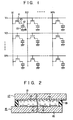
- Figs. 1 and 2 show an equivalent circuit of an active matrix type display apparatus having a TFT array and a schematic sectional view thereof.
- reference numeral 11 denotes a TFT as a switching element; and 12, a display pixel electrode which is connected to the source of the TFT 11 through a connecting portion 10.
- the connecting portion 10 is a small region which connects the source of the TFT 11 with the display pixel electrode 12 having a large area.
- the connecting portion 10 can be integrally formed with the display pixel electrode 12 and the source electrode of the TFT 11, or can be formed of a different conductive material. Gates of the TFTs 11 of each row are commonly connected to respective gate buses Y1, Y2,..., Yn.
- a first electrode substrate 15 comprises a transparent insulating substrate 16 formed of, e.g., glass on which the TFT array (not shown) and the display pixel electrode 12 driven thereby are formed.
- a second electrode substrate 17 comprises a transparent insulating substrate 18 formed of, e.g., glass on which the opposing electrode 13 formed of a transparent conductive film is formed.
- the liquid crystal layer 14 is sandwiched between these first and second electrode substrates 15 and 17.
- Reference numeral 19 denotes a spacer or sealing portion.
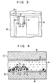
- FIG. 3 is a plan view showing a pattern of the first electrode substrate 15, and Fig. 4 is a detailed sectional view thereof.
- the first electrode substrate 15 can be obtained in the following manner.
- a drain electrode 20 formed of a transparent conductive film, the display pixel electrode 12 and a source electrode 21 integrally formed with the connecting portion 10 are formed on the transparent insulation substrate 16.
- a semiconductor thin film 22 is deposited on the thus obtained structure.
- a gate electrode 24 formed of, e.g., an At film is formed on the semiconductor thin film 22 through a gate insulating film 23.
- a passivating film 25 formed of, e.g., an 5i0 2 film is formed on the resultant structure, thus obtaining the first electrode substrate 15.
- the gate buses Y1, Y2,..., Yn are sequentially scanned and driven by a scanning signal.
- the TFTs 11 are sequentially turned on by each gate bus during a time period of T f/ n.
- Tf here means a frame scanning period.
- a TFT is easily subjected to light influence.
- a hydrogenated amorphous silicon film a-Si : H
- conductivity becomes more than thousand times of that upon irradiation with light.
- a leakage current is increased, thereby degrading performance of a transmission type display apparatus.
- a light shielding layer must be provided on the TFT portion.
- the signal voltage supplied through the TFT 11 and the connecting portion 10 is stored by a capacitor consisting of the display pixel electrode 12, the opposing electrode 13 and the liquid crystal layer 14.
- a supplemental storage capacitor is connected in parallel to the capacitance of the liquid crystal layer 14.
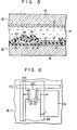
- a capacitor electrode 26 formed of a transparent conductive film is formed on the transparent insulating substrate 16, as shown in Fig. 5.
- an insulating film 27 formed of, e.g., an 5i0 2 film is formed on the capacitor electrode 26.
- the TFT array and the display pixel electrode 12 are formed in the same manner as in Fig. 4.
- an electrically conductive light shielding layer is provided on a TFT portion of a first electrode substrate and is set at a predetermined potential, and a part thereof opposes a part of a display pixel electrode through an insulating film so as to form an supplemental storage capacitor.
- the TFT portion is covered by the light shielding layer, and the supplemental storage capacitor is formed between the light shielding layer and the display pixel elelctrode, thereby obtaining a transmission type display apparatus having a good resistance to ambient light and a high signal-voltage storing property. Furthermore, according to the present invention, since the light shielding layer also serves as the supplemental storage capacitor electrode, the manufacturing process does not become complicated and the number of steps is not increased, and therefore a high manufacturing yield can be obtained.
- Figs. 6 and 7 show a structure of one pixel portion according to this embodiment of the present invention corresponding to Figs. 3 and 4, respectively. Therefore, the same reference numerals as in Figs. 3 and 4 denote the same parts in Figs. 6 and 7 and a detailed description thereof is omitted.
- the appparatus shown in Figs. 6 and 7 is different from the conventional apparatus in that an electrically conductive light shielding layer 28 is formed on a transparent insulating substrate 16 so as to cover a TFT region before forming a TFT 11, a display pixel electrode 12 and a connecting portion 10.
- This light shielding layer 28 comprises a metal film formed of, e.g., At, Mo or Cr.
- a silicon nitride film 29 serving as an insulating film is formed on the light shielding layer 28, and the TFT 11 and the display pixel electrode 12 are formed thereon.
- each light shielding layer 28 is commonly provided along a column direction and is set at a predetermined potential such as a ground potential by an external circuit. This is because, if not, a drain electrode of the TFT 11 causes capacitive coupling with a source electrode 21 through the light shielding layer 28.
- the predetermined potential is not limited to the ground potential. In addtion, if the light shielding layer 28 opposes the entire surface of the display pixel electrode 12, transmission display cannot be performed.
- the light shielding layer 28 is formed to overlap a part of the display pixel electrode 12, and this overlapped portion forms the supplemental storage capacitor.
- the connecting portion 10 also forms a capacitor with the light shielding layer 28 and forms a portion of the supplemental storage capacitor.
- a capacitance C 1 of this supplemental storage capacitor can be determined by a permittivity and a thickness of the silicon nitride film 29 and an overlapped area of the light shielding layer 28, the display pixel electrode 12 and the connecting portion 10.
- a capacitance C 1 0.5 - 1 pF can easily be obtained by an overlapped area which is not so large as to practically affect light transmission at the display pixel portion.
- the capacitance C 1 was 0.85 pF.
- a capacitance formed in the overlapped portion of the connecting portion 10 and the light shielding layer 28 was in the order of 0.01 pF and contribution to the supplemental storage capacitor was extremely small.
- the display pixel electrode 12, the opposing electrode 13 and the liquid crystal layer 14 formed therebetween serve as a signal voltage storing capacitor.
- a pixel area S is 150 ⁇ m x 150 ⁇ m
- a dielectric constant ⁇ of a liquid crystal material is 8, and a thickness t of a cell is 8 ⁇ m
- a capacitance C 2 of this capacitor is about 0.2 pF.
- a display electrode potential drops to 1/3 or less of the initial potential V O , thereby undesirably decreasing an effective voltage applied to the liquid crystal layer and degrading the performance of the LCD.
- the manufacturing process does not become complicated and the number of steps is not increased, thereby improving a yield.
- Fig. 8 is a sectional view of one pixel portion according to another embodiment of the present invention corresponding to Fig. 7.
- a TFT 11 has a vertically inverted structure of that of the above embodiment.
- the same reference numerals as in Fig. 7 denote the same parts in Fig. 8.
- a gate electrode 24 of the TFT 11 is directly formed on a transparent insulating substrate 16. Since incidence of light from a side of a second electrode substrate 17 causes a problem, a light shielding layer 28 is formed on the TFT 11 and a display pixel electrode 12.
- the light shielding layer 28 overlaps with a part of the display pixel electrode 12 and a connecting portion 10 through a silicon nitride film 29, thereby constructing a supplemental storage capacitor in the same manner as in the above embodiment.
- the same effect as in the above embodiment can be obtained from this embodiment.
- a gate insulating film and an insulation film between a light shielding layer and a display pixel electrode are not limited to a silicon oxide film and silicon nitride film, but can be formed of an inorganic insulation film such as a silicon oxynitride film, or of an organic insulation film of, for example, polyimide.
- a light shielding layer can be formed of any conductive material which do not transmit light therethrough.
- this layer can be formed of a material having a relatively high resistance and can be a thin film of 1,000 A to 2,000 A.
- Each of the above-mentioned layers can be formed by plasma CVD, normal pressure or low pressure CVD, deposition, sputtering, molecular beam epitaxy, spin-on glass, or the like.
- a transparent electrode is directly formed as an opposing electrode on a transparent substrate in the above embodiments, the transparent electrode can be formed on a color filter formed on an insulating substrate, or the color filter can be provided after forming the transparent electrode.
- the present invention can be effectively applied to a display apparatus using an EL thin film instead of a liquid crystal material.
Abstract
Description
- The present invention relates to an active matrix type display apparatus of transmission type using a thin film transistor (TFT) array.
- Currently, a display apparatus using a liquid crystal material, an electroluminescent (EL) film or the like, which is a large-capacity and high-density active matrix type display apparatus used for television or graphic display, has been developed for practical use. In such a display apparatus, a semiconductor switch for driving and controlling each pixel is used so as to perform high-contrast display without cross-talk. MOSFETs formed on a single crystalline Si substrate or TFTs formed on a transparent substrate which can perform transmission type display are used as such semiconductor switches.
- Figs. 1 and 2 show an equivalent circuit of an active matrix type display apparatus having a TFT array and a schematic sectional view thereof. In Fig. 1, reference numeral 11 denotes a TFT as a switching element; and 12, a display pixel electrode which is connected to the source of the TFT 11 through a connecting
portion 10. The connectingportion 10 is a small region which connects the source of the TFT 11 with thedisplay pixel electrode 12 having a large area. The connectingportion 10 can be integrally formed with thedisplay pixel electrode 12 and the source electrode of the TFT 11, or can be formed of a different conductive material. Gates of the TFTs 11 of each row are commonly connected to respective gate buses Y1, Y2,..., Yn. Drains of the TFTs 11 of each column are commonly connected to respective drain buses X1, X2,..., Xm.Reference numeral 13 denotes an opposing electrode; and 14, a liquid crystal layer. In Fig. 2, afirst electrode substrate 15 comprises a transparentinsulating substrate 16 formed of, e.g., glass on which the TFT array (not shown) and thedisplay pixel electrode 12 driven thereby are formed. Asecond electrode substrate 17 comprises a transparentinsulating substrate 18 formed of, e.g., glass on which theopposing electrode 13 formed of a transparent conductive film is formed. Theliquid crystal layer 14 is sandwiched between these first andsecond electrode substrates Reference numeral 19 denotes a spacer or sealing portion. - A specific structure of one pixel portion is as shown in Figs. 3 and 4. Fig. 3 is a plan view showing a pattern of the
first electrode substrate 15, and Fig. 4 is a detailed sectional view thereof. Thefirst electrode substrate 15 can be obtained in the following manner. Adrain electrode 20 formed of a transparent conductive film, thedisplay pixel electrode 12 and asource electrode 21 integrally formed with the connectingportion 10 are formed on thetransparent insulation substrate 16. A semiconductorthin film 22 is deposited on the thus obtained structure. Then, agate electrode 24 formed of, e.g., an At film is formed on the semiconductorthin film 22 through agate insulating film 23. Thereafter, apassivating film 25 formed of, e.g., an 5i02 film is formed on the resultant structure, thus obtaining thefirst electrode substrate 15. - In the above structure, the operation of the liquid crystal display apparatus is performed in the following manner. The gate buses Y1, Y2,..., Yn are sequentially scanned and driven by a scanning signal. The TFTs 11 are sequentially turned on by each gate bus during a time period of Tf/n. Note that "Tf" here means a frame scanning period. When, for example, m parallel image signal voltages are applied to the drain buses X1, X2,..., Xm in synchronism with this scanning operation, the signal voltages are sequentially coupled to the
display pixel electrodes 12 by each gate bus. Then, the signal voltage excites theliquid crystal layer 14 sandwiched between thedisplay electrode 12 and theopposing electrode 13, thereby performing image display. - In this display apparatus, a TFT is easily subjected to light influence. Particularly, when a hydrogenated amorphous silicon film (a-Si : H) is used as a semiconductor film, conductivity becomes more than thousand times of that upon irradiation with light. When the TFT is turned off, therefore, a leakage current is increased, thereby degrading performance of a transmission type display apparatus. In order to compensate for this disadvantage, a light shielding layer must be provided on the TFT portion.
- In addition, in this display apparatus, the signal voltage supplied through the TFT 11 and the connecting
portion 10 is stored by a capacitor consisting of thedisplay pixel electrode 12, theopposing electrode 13 and theliquid crystal layer 14. However, in many applications, since a leakage current flows in theliquid crystal layer 14, the stored signal voltage is attenuated before the TFT 11 is next driven. In order to prevent this disadvantage, a supplemental storage capacitor is connected in parallel to the capacitance of theliquid crystal layer 14. In this case, acapacitor electrode 26 formed of a transparent conductive film is formed on the transparentinsulating substrate 16, as shown in Fig. 5. Then, aninsulating film 27 formed of, e.g., an 5i02 film is formed on thecapacitor electrode 26. Thereafter, the TFT array and thedisplay pixel electrode 12 are formed in the same manner as in Fig. 4. - However, when a light shielding layer and a capacitor electrode are separately provided as described above, the number of manufacturing steps is increased, thereby degrading a yield of the display apparatus.
- It is an object of the present invention to provide an active matrix type display apparatus having high performance in which a high manufacturing yield can be obtained without increasing the number of manufacturing steps.
- In an active matrix type display apparatus of the present invention, an electrically conductive light shielding layer is provided on a TFT portion of a first electrode substrate and is set at a predetermined potential, and a part thereof opposes a part of a display pixel electrode through an insulating film so as to form an supplemental storage capacitor.
- According to the present invention, the TFT portion is covered by the light shielding layer, and the supplemental storage capacitor is formed between the light shielding layer and the display pixel elelctrode, thereby obtaining a transmission type display apparatus having a good resistance to ambient light and a high signal-voltage storing property. Furthermore, according to the present invention, since the light shielding layer also serves as the supplemental storage capacitor electrode, the manufacturing process does not become complicated and the number of steps is not increased, and therefore a high manufacturing yield can be obtained.
- This invention can be more fully understood from the following detailed description when taken in conjunction with the accompanying drawings, in which:
- Fig. 1 is a circuit diagram showing an equivalent circuit of a conventional active matrix type display apparatus;
- Fig. 2 is a schematic sectional view showing the entire structure of the conventional display apparatus of Fig. 1;
- Fig. 3 is a plan view showing a pattern of one pixel portion of the conventional display apparatus of Fig. 1;
- Fig. 4 is a sectional view of the one pixel portion of Fig. 3;
- Fig. 5 is a sectional view showing the conventional active matrix type display apparatus having a supplemental storage capacitor corresponding to Fig. 4;
- Figs. 6 and 7 are respectively views showing one pixel portion of an active matrix type display apparatus according to an embodiment of the present invention corresponding to Figs. 3 and 4; and
- Fig. 8 is a view showing a structure of one pixel portion according to another embodiment of the present invention corresponding to Fig. 7.
- An embodiment of the present invention will be described hereinafter.
- Figs. 6 and 7 show a structure of one pixel portion according to this embodiment of the present invention corresponding to Figs. 3 and 4, respectively. Therefore, the same reference numerals as in Figs. 3 and 4 denote the same parts in Figs. 6 and 7 and a detailed description thereof is omitted. The appparatus shown in Figs. 6 and 7 is different from the conventional apparatus in that an electrically conductive
light shielding layer 28 is formed on a transparentinsulating substrate 16 so as to cover a TFT region before forming a TFT 11, adisplay pixel electrode 12 and a connectingportion 10. Thislight shielding layer 28 comprises a metal film formed of, e.g., At, Mo or Cr. Asilicon nitride film 29 serving as an insulating film is formed on thelight shielding layer 28, and the TFT 11 and thedisplay pixel electrode 12 are formed thereon. It should be noted that eachlight shielding layer 28 is commonly provided along a column direction and is set at a predetermined potential such as a ground potential by an external circuit. This is because, if not, a drain electrode of the TFT 11 causes capacitive coupling with asource electrode 21 through thelight shielding layer 28. The predetermined potential is not limited to the ground potential. In addtion, if thelight shielding layer 28 opposes the entire surface of thedisplay pixel electrode 12, transmission display cannot be performed. For this reason, thelight shielding layer 28 is formed to overlap a part of thedisplay pixel electrode 12, and this overlapped portion forms the supplemental storage capacitor. In this embodiment, the connectingportion 10 also forms a capacitor with thelight shielding layer 28 and forms a portion of the supplemental storage capacitor. - The effect of the thus formed supplemental storage capacitor using the
light shielding layer 28 will now be described in detail. - A capacitance C1 of this supplemental storage capacitor can be determined by a permittivity and a thickness of the
silicon nitride film 29 and an overlapped area of thelight shielding layer 28, thedisplay pixel electrode 12 and the connectingportion 10. A capacitance C1 = 0.5 - 1 pF can easily be obtained by an overlapped area which is not so large as to practically affect light transmission at the display pixel portion. When a size of thedisplay pixel electrode 12 was given by 165 µm x 150 µm and a width L of the overlapped portion was given by 15 µm, the capacitance C1 was 0.85 pF. A capacitance formed in the overlapped portion of the connectingportion 10 and thelight shielding layer 28 was in the order of 0.01 pF and contribution to the supplemental storage capacitor was extremely small. - On the other hand, the
display pixel electrode 12, the opposingelectrode 13 and theliquid crystal layer 14 formed therebetween serve as a signal voltage storing capacitor. In the case wherein a pixel area S is 150 µm x 150 µm, a dielectric constant ε of a liquid crystal material is 8, and a thickness t of a cell is 8 µm, a capacitance C2 of this capacitor is about 0.2 pF. When a resistivity of a liquid crystal material is given by a typical value of a guest-host type liquid crystal of ρLC = 2 x 10¹⁰ Ω·cm, a resistance of theliquid crystal layer 14 is expressed by;
- Furthermore, in this embodiment, since the light shielding layer serves as the supplemental storage capacitor, the manufacturing process does not become complicated and the number of steps is not increased, thereby improving a yield.
- Fig. 8 is a sectional view of one pixel portion according to another embodiment of the present invention corresponding to Fig. 7. A TFT 11 has a vertically inverted structure of that of the above embodiment. The same reference numerals as in Fig. 7 denote the same parts in Fig. 8. In this embodiment, a
gate electrode 24 of the TFT 11 is directly formed on a transparent insulatingsubstrate 16. Since incidence of light from a side of asecond electrode substrate 17 causes a problem, alight shielding layer 28 is formed on the TFT 11 and adisplay pixel electrode 12. Thelight shielding layer 28 overlaps with a part of thedisplay pixel electrode 12 and a connectingportion 10 through asilicon nitride film 29, thereby constructing a supplemental storage capacitor in the same manner as in the above embodiment. The same effect as in the above embodiment can be obtained from this embodiment. - The present invention can be effectively adopted not only in an apparatus using poly-Si or a-Si : H, but also in an apparatus using poly-Si or a compound semiconductor such as, CdSe or CdS. A gate insulating film and an insulation film between a light shielding layer and a display pixel electrode are not limited to a silicon oxide film and silicon nitride film, but can be formed of an inorganic insulation film such as a silicon oxynitride film, or of an organic insulation film of, for example, polyimide. Furthermore, a light shielding layer can be formed of any conductive material which do not transmit light therethrough. In addition, since almost no current flows therein, this layer can be formed of a material having a relatively high resistance and can be a thin film of 1,000 A to 2,000 A. Each of the above-mentioned layers can be formed by plasma CVD, normal pressure or low pressure CVD, deposition, sputtering, molecular beam epitaxy, spin-on glass, or the like. Furthermore, although a transparent electrode is directly formed as an opposing electrode on a transparent substrate in the above embodiments, the transparent electrode can be formed on a color filter formed on an insulating substrate, or the color filter can be provided after forming the transparent electrode.
- Although a liquid crystal display apparatus has been described in the above embodiments, the present invention can be effectively applied to a display apparatus using an EL thin film instead of a liquid crystal material.
Claims (4)
Applications Claiming Priority (2)
| Application Number | Priority Date | Filing Date | Title |
|---|---|---|---|
| JP58153771A JPS6045219A (en) | 1983-08-23 | 1983-08-23 | Active matrix type display device |
| JP153771/83 | 1983-08-23 |
Publications (3)
| Publication Number | Publication Date |
|---|---|
| EP0136509A2 true EP0136509A2 (en) | 1985-04-10 |
| EP0136509A3 EP0136509A3 (en) | 1986-09-03 |
| EP0136509B1 EP0136509B1 (en) | 1989-05-31 |
Family
ID=15569776
Family Applications (1)
| Application Number | Title | Priority Date | Filing Date |
|---|---|---|---|
| EP84109905A Expired EP0136509B1 (en) | 1983-08-23 | 1984-08-20 | Active matrix type display apparatus |
Country Status (4)
| Country | Link |
|---|---|
| US (1) | US4759610A (en) |
| EP (1) | EP0136509B1 (en) |
| JP (1) | JPS6045219A (en) |
| DE (1) | DE3478514D1 (en) |
Cited By (26)
| Publication number | Priority date | Publication date | Assignee | Title |
|---|---|---|---|---|
| EP0197703A1 (en) * | 1985-04-03 | 1986-10-15 | THE GENERAL ELECTRIC COMPANY, p.l.c. | Liquid crystal displays |
| EP0198168A1 (en) * | 1985-02-21 | 1986-10-22 | OIS Optical Imaging Systems, Inc. | Active matrix liquid crystal displays and method of making them |
| EP0269123A2 (en) * | 1986-11-27 | 1988-06-01 | Nec Corporation | A thin film transistor array for liquid crystal display panel |
| US4778258A (en) * | 1987-10-05 | 1988-10-18 | General Electric Company | Protective tab structure for use in the fabrication of matrix addressed thin film transistor liquid crystal displays |
| EP0329887A1 (en) * | 1988-02-25 | 1989-08-30 | Sharp Kabushiki Kaisha | Liquid crystal display device |
| EP0341003A2 (en) * | 1988-04-30 | 1989-11-08 | Sharp Kabushiki Kaisha | Thin film semiconductor device and liquid crystal display apparatus using thereof |
| EP0376437A2 (en) * | 1988-08-10 | 1990-07-04 | Sharp Kabushiki Kaisha | An active matrix type liquid crystal display |
| US5066110A (en) * | 1988-12-26 | 1991-11-19 | Sharp Kabushiki Kaisha | Liquid crystal display apparatus |
| EP0464897A2 (en) * | 1990-06-27 | 1992-01-08 | Philips Electronics Uk Limited | Active matrix liquid crystal display devices |
| EP0481734A2 (en) * | 1990-10-16 | 1992-04-22 | Agency Of Industrial Science And Technology | Light valve device |
| EP0524067A1 (en) * | 1991-07-11 | 1993-01-20 | France Telecom | High definition active matrix liquid crystal screen |
| US5187551A (en) * | 1988-04-30 | 1993-02-16 | Sharp Kabushiki Kaisha | Thin film semiconductor device and liquid crystal display apparatus thereof for preventing irradiated light from reaching the semiconductor layers |
| WO1993007529A1 (en) * | 1991-10-11 | 1993-04-15 | Thomson-Lcd | Active matrix display device using a buried ground plane |
| US5231039A (en) * | 1988-02-25 | 1993-07-27 | Sharp Kabushiki Kaisha | Method of fabricating a liquid crystal display device |
| EP0556484A1 (en) * | 1991-12-25 | 1993-08-25 | Kabushiki Kaisha Toshiba | Liquid crystal display device |
| FR2689287A1 (en) * | 1992-03-30 | 1993-10-01 | France Telecom | Optical mask display screen and method of producing this screen. |
| EP0592063A2 (en) * | 1992-09-14 | 1994-04-13 | Kabushiki Kaisha Toshiba | Active matrix liquid crystal display device |
| EP0595363A1 (en) * | 1992-10-30 | 1994-05-04 | Nec Corporation | Transmission type active matrix liquid crystal device |
| EP0604006A2 (en) * | 1992-10-27 | 1994-06-29 | Nec Corporation | Active matrix liquid crystal display cell |
| US5434433A (en) * | 1992-08-19 | 1995-07-18 | Seiko Instruments Inc. | Semiconductor device for a light wave |
| EP0725301A1 (en) * | 1995-01-31 | 1996-08-07 | Nec Corporation | Active matrix liquid crystal display device with light shielding electrode connected to an independent potential |
| WO1996036998A1 (en) * | 1995-05-16 | 1996-11-21 | Thomson-Lcd | Method for making direct multistage tft devices with grid-source or drain interconnection |
| US5633176A (en) * | 1992-08-19 | 1997-05-27 | Seiko Instruments Inc. | Method of producing a semiconductor device for a light valve |
| EP0782035A1 (en) * | 1995-12-29 | 1997-07-02 | Xerox Corporation | Method of forming array of light active cells and array |
| EP0997769A2 (en) * | 1998-10-28 | 2000-05-03 | Sony Corporation | Active matrix liquid crystal display device |
| US6191476B1 (en) | 1992-10-21 | 2001-02-20 | Seiko Instruments Inc. | Semiconductor device |
Families Citing this family (136)
| Publication number | Priority date | Publication date | Assignee | Title |
|---|---|---|---|---|
| JP3307150B2 (en) * | 1995-03-20 | 2002-07-24 | ソニー株式会社 | Active matrix display |
| US4904061A (en) * | 1984-10-22 | 1990-02-27 | Seiko Epson Corporation | Projection-type liquid crystal display device with even color |
| DE3524085A1 (en) * | 1985-07-05 | 1987-01-08 | Vdo Schindling | LIQUID CRYSTAL CELL |
| JPS6280626A (en) * | 1985-10-04 | 1987-04-14 | Hosiden Electronics Co Ltd | Liquid crystal display element |
| JPS6319876A (en) * | 1986-07-11 | 1988-01-27 | Fuji Xerox Co Ltd | Thin film transistor device |
| US5191450A (en) * | 1987-04-14 | 1993-03-02 | Seiko Epson Corporation | Projection-type color display device having a driving circuit for producing a mirror-like image |
| EP0287034B1 (en) * | 1987-04-14 | 1995-01-18 | Seiko Epson Corporation | Projection-type color display device |
| JP2620240B2 (en) | 1987-06-10 | 1997-06-11 | 株式会社日立製作所 | Liquid crystal display |
| JPS64930A (en) * | 1987-06-24 | 1989-01-05 | Alps Electric Co Ltd | Liquid crystal element |
| US4918504A (en) * | 1987-07-31 | 1990-04-17 | Nippon Telegraph And Telephone Corporation | Active matrix cell |
| US5198377A (en) * | 1987-07-31 | 1993-03-30 | Kinya Kato | Method of manufacturing an active matrix cell |
| US4943839A (en) * | 1987-08-19 | 1990-07-24 | Ricoh Company, Ltd. | Contact type image sensor |
| US4839707A (en) * | 1987-08-27 | 1989-06-13 | Hughes Aircraft Company | LCMOS displays fabricated with implant treated silicon wafers |
| US5327001A (en) * | 1987-09-09 | 1994-07-05 | Casio Computer Co., Ltd. | Thin film transistor array having single light shield layer over transistors and gate and drain lines |
| US5229644A (en) * | 1987-09-09 | 1993-07-20 | Casio Computer Co., Ltd. | Thin film transistor having a transparent electrode and substrate |
| JPH01302769A (en) * | 1988-05-30 | 1989-12-06 | Seikosha Co Ltd | Manufacture of inverse stagger type si thin film transistor |
| US5042918A (en) * | 1988-11-15 | 1991-08-27 | Kabushiki Kaisha Toshiba | Liquid crystal display device |
| KR920008056B1 (en) * | 1988-11-30 | 1992-09-22 | 주식회사 금성사 | Thin film lcd matrix of thin film lcd color tv |
| US4990460A (en) * | 1989-01-27 | 1991-02-05 | Nec Corporation | Fabrication method for thin film field effect transistor array suitable for liquid crystal display |
| JP2600929B2 (en) * | 1989-01-27 | 1997-04-16 | 松下電器産業株式会社 | Liquid crystal image display device and method of manufacturing the same |
| US5270229A (en) * | 1989-03-07 | 1993-12-14 | Matsushita Electric Industrial Co., Ltd. | Thin film semiconductor device and process for producing thereof |
| JPH0734467B2 (en) * | 1989-11-16 | 1995-04-12 | 富士ゼロックス株式会社 | Image sensor manufacturing method |
| EP0438138B1 (en) * | 1990-01-17 | 1995-03-15 | Kabushiki Kaisha Toshiba | Liquid-crystal display device of active matrix type |
| JPH07112053B2 (en) * | 1990-04-13 | 1995-11-29 | 富士ゼロックス株式会社 | Thin film switching element array |
| JPH0453929A (en) * | 1990-06-22 | 1992-02-21 | Fujitsu Ltd | Reflection type liquid crystal device |
| JP3226223B2 (en) * | 1990-07-12 | 2001-11-05 | 株式会社東芝 | Thin film transistor array device and liquid crystal display device |
| US5402254B1 (en) * | 1990-10-17 | 1998-09-22 | Hitachi Ltd | Liquid crystal display device with tfts in which pixel electrodes are formed in the same plane as the gate electrodes with anodized oxide films before the deposition of silicon |
| US5618739A (en) * | 1990-11-15 | 1997-04-08 | Seiko Instruments Inc. | Method of making light valve device using semiconductive composite substrate |
| US5347154A (en) * | 1990-11-15 | 1994-09-13 | Seiko Instruments Inc. | Light valve device using semiconductive composite substrate |
| US5177475A (en) * | 1990-12-19 | 1993-01-05 | Xerox Corporation | Control of liquid crystal devices |
| US5475514A (en) * | 1990-12-31 | 1995-12-12 | Kopin Corporation | Transferred single crystal arrayed devices including a light shield for projection displays |
| US6556257B2 (en) * | 1991-09-05 | 2003-04-29 | Sony Corporation | Liquid crystal display device |
| JP2900662B2 (en) * | 1991-10-18 | 1999-06-02 | 三菱電機株式会社 | Thin film transistor array |
| FR2687844A1 (en) * | 1992-02-26 | 1993-08-27 | Chouan Yannick | PROCESS FOR PRODUCING A DUAL GRID THIN FILM TRANSISTOR AND OPTICAL MASK |
| JP3205373B2 (en) * | 1992-03-12 | 2001-09-04 | 株式会社日立製作所 | Liquid crystal display |
| JP2543286B2 (en) * | 1992-04-22 | 1996-10-16 | インターナショナル・ビジネス・マシーンズ・コーポレイション | Liquid crystal display |
| GB9211283D0 (en) * | 1992-05-28 | 1992-07-15 | Philips Electronics Uk Ltd | Liquid crystal display devices |
| KR960006205B1 (en) * | 1992-12-30 | 1996-05-09 | 엘지전자주식회사 | The structure of tft-lcd |
| JP2812851B2 (en) * | 1993-03-24 | 1998-10-22 | シャープ株式会社 | Reflective liquid crystal display |
| JP2975844B2 (en) * | 1993-06-24 | 1999-11-10 | 三洋電機株式会社 | Liquid crystal display |
| KR0141774B1 (en) * | 1994-06-17 | 1998-06-15 | 구자홍 | Liquid crystal display device and its manufacturing method |
| TW289097B (en) * | 1994-08-24 | 1996-10-21 | Hitachi Ltd | |
| JPH0887034A (en) * | 1994-09-16 | 1996-04-02 | Toshiba Corp | Liquid crystal display and its production |
| TW347477B (en) * | 1994-09-30 | 1998-12-11 | Sanyo Electric Co | Liquid crystal display with storage capacitors for holding electric charges |
| FR2731526B1 (en) * | 1995-03-09 | 1997-04-04 | Thomson Consumer Electronics | LIQUID CRYSTAL SCREEN WITH IMPROVED ANGLE OF VIEW |
| JPH0926603A (en) * | 1995-05-08 | 1997-01-28 | Semiconductor Energy Lab Co Ltd | Display device |
| KR970011972A (en) * | 1995-08-11 | 1997-03-29 | 쯔지 하루오 | Transmission type liquid crystal display device and manufacturing method thereof |
| KR0171102B1 (en) * | 1995-08-29 | 1999-03-20 | 구자홍 | Liquid crystal display device structure and manufacturing method |
| JP3184771B2 (en) * | 1995-09-14 | 2001-07-09 | キヤノン株式会社 | Active matrix liquid crystal display |
| JPH0990397A (en) * | 1995-09-28 | 1997-04-04 | Sharp Corp | Active matrix substrate and display device formed by using the same |
| JP3272212B2 (en) * | 1995-09-29 | 2002-04-08 | シャープ株式会社 | Transmissive liquid crystal display device and method of manufacturing the same |
| TW439003B (en) * | 1995-11-17 | 2001-06-07 | Semiconductor Energy Lab | Display device |
| US6800875B1 (en) | 1995-11-17 | 2004-10-05 | Semiconductor Energy Laboratory Co., Ltd. | Active matrix electro-luminescent display device with an organic leveling layer |
| JPH09146108A (en) | 1995-11-17 | 1997-06-06 | Semiconductor Energy Lab Co Ltd | Liquid crystal display device and its driving method |
| JP2720862B2 (en) * | 1995-12-08 | 1998-03-04 | 日本電気株式会社 | Thin film transistor and thin film transistor array |
| TW309633B (en) * | 1995-12-14 | 1997-07-01 | Handotai Energy Kenkyusho Kk | |
| US6682961B1 (en) | 1995-12-29 | 2004-01-27 | Samsung Electronics Co., Ltd. | Thin film transistor array panel used for a liquid crystal display and a manufacturing method thereof |
| JP3729955B2 (en) * | 1996-01-19 | 2005-12-21 | 株式会社半導体エネルギー研究所 | Method for manufacturing semiconductor device |
| US6478263B1 (en) | 1997-01-17 | 2002-11-12 | Semiconductor Energy Laboratory Co., Ltd. | Semiconductor device and its manufacturing method |
| JP3645378B2 (en) | 1996-01-19 | 2005-05-11 | 株式会社半導体エネルギー研究所 | Method for manufacturing semiconductor device |
| JP3645380B2 (en) * | 1996-01-19 | 2005-05-11 | 株式会社半導体エネルギー研究所 | Manufacturing method of semiconductor device, information terminal, head mounted display, navigation system, mobile phone, video camera, projection display device |
| JP3645379B2 (en) | 1996-01-19 | 2005-05-11 | 株式会社半導体エネルギー研究所 | Method for manufacturing semiconductor device |
| US7056381B1 (en) | 1996-01-26 | 2006-06-06 | Semiconductor Energy Laboratory Co., Ltd. | Fabrication method of semiconductor device |
| US6180439B1 (en) | 1996-01-26 | 2001-01-30 | Semiconductor Energy Laboratory Co., Ltd. | Method for fabricating a semiconductor device |
| JP3647542B2 (en) * | 1996-02-20 | 2005-05-11 | 株式会社半導体エネルギー研究所 | Liquid crystal display |
| JP3205501B2 (en) * | 1996-03-12 | 2001-09-04 | シャープ株式会社 | Active matrix display device and repair method thereof |
| US6100562A (en) | 1996-03-17 | 2000-08-08 | Semiconductor Energy Laboratory Co., Ltd. | Method of manufacturing a semiconductor device |
| JP2734444B2 (en) * | 1996-03-22 | 1998-03-30 | 日本電気株式会社 | Liquid crystal display |
| JP3468986B2 (en) * | 1996-04-16 | 2003-11-25 | 株式会社半導体エネルギー研究所 | Active matrix circuit and display device |
| JP3685869B2 (en) | 1996-05-08 | 2005-08-24 | 株式会社半導体エネルギー研究所 | Liquid crystal display device |
| US6005648A (en) * | 1996-06-25 | 1999-12-21 | Semiconductor Energy Laboratory Co., Ltd. | Display device |
| JP3126661B2 (en) * | 1996-06-25 | 2001-01-22 | 株式会社半導体エネルギー研究所 | Liquid crystal display |
| JPH1020298A (en) * | 1996-07-03 | 1998-01-23 | Sharp Corp | Liquid crystal display device |
| JP3708637B2 (en) * | 1996-07-15 | 2005-10-19 | 株式会社半導体エネルギー研究所 | Liquid crystal display device |
| JP3634089B2 (en) * | 1996-09-04 | 2005-03-30 | 株式会社半導体エネルギー研究所 | Display device |
| TWI236556B (en) | 1996-10-16 | 2005-07-21 | Seiko Epson Corp | Substrate for a liquid crystal equipment, liquid crystal equipment and projection type display equipment |
| WO1998018044A1 (en) * | 1996-10-22 | 1998-04-30 | Seiko Epson Corporation | Active matrix liquid crystal panel |
| US7872728B1 (en) | 1996-10-22 | 2011-01-18 | Seiko Epson Corporation | Liquid crystal panel substrate, liquid crystal panel, and electronic device and projection display device using the same |
| JP3716580B2 (en) * | 1997-02-27 | 2005-11-16 | セイコーエプソン株式会社 | Liquid crystal device and manufacturing method thereof, and projection display device |
| JP3784491B2 (en) | 1997-03-28 | 2006-06-14 | 株式会社半導体エネルギー研究所 | Active matrix display device |
| TW508470B (en) * | 1997-05-09 | 2002-11-01 | Hitachi Ltd | Liquid crystal display device |
| JP4396599B2 (en) * | 1997-10-31 | 2010-01-13 | セイコーエプソン株式会社 | Liquid crystal device, electronic apparatus, and projection display device |
| JPH11202349A (en) * | 1998-01-12 | 1999-07-30 | Semiconductor Energy Lab Co Ltd | Display device |
| CN101533192B (en) * | 1998-02-09 | 2011-08-03 | 精工爱普生株式会社 | Electrooptical panel and electronic appliances |
| GB9803764D0 (en) * | 1998-02-23 | 1998-04-15 | Cambridge Display Tech Ltd | Display devices |
| JP4312851B2 (en) | 1998-04-27 | 2009-08-12 | 株式会社半導体エネルギー研究所 | Semiconductor device and manufacturing method thereof |
| JP3941901B2 (en) * | 1998-04-28 | 2007-07-11 | 株式会社半導体エネルギー研究所 | Method for manufacturing semiconductor device |
| GB9811477D0 (en) * | 1998-05-29 | 1998-07-29 | Sharp Kk | Liquid crystal device |
| KR100333179B1 (en) | 1998-06-30 | 2002-08-24 | 주식회사 현대 디스플레이 테크놀로지 | Thin film transistor liquid crystal display device and manufacturing method thereof |
| US6313481B1 (en) | 1998-08-06 | 2001-11-06 | Semiconductor Energy Laboratory Co., Ltd. | Semiconductor device and a method of manufacturing the same |
| US6475836B1 (en) | 1999-03-29 | 2002-11-05 | Semiconductor Energy Laboratory Co., Ltd. | Semiconductor device and manufacturing method thereof |
| US7288420B1 (en) * | 1999-06-04 | 2007-10-30 | Semiconductor Energy Laboratory Co., Ltd. | Method for manufacturing an electro-optical device |
| JP2001109404A (en) * | 1999-10-01 | 2001-04-20 | Sanyo Electric Co Ltd | El display device |
| GB9928353D0 (en) * | 1999-12-01 | 2000-01-26 | Koninkl Philips Electronics Nv | Liquid crystal display and method of manufacture |
| US6590227B2 (en) * | 1999-12-27 | 2003-07-08 | Semiconductor Energy Laboratory Co., Ltd. | Active matrix display device |
| TW521303B (en) * | 2000-02-28 | 2003-02-21 | Semiconductor Energy Lab | Electronic device |
| GB0014962D0 (en) * | 2000-06-20 | 2000-08-09 | Koninkl Philips Electronics Nv | Matrix array display devices with light sensing elements and associated storage capacitors |
| US20020097350A1 (en) * | 2000-09-19 | 2002-07-25 | Haven Duane A. | Thin film transistors suitable for use in flat panel displays |
| DE10057696A1 (en) * | 2000-11-21 | 2002-05-16 | Siemens Ag | LCD display with background lighting provided by a controlled light source |
| US6897477B2 (en) * | 2001-06-01 | 2005-05-24 | Semiconductor Energy Laboratory Co., Ltd. | Semiconductor device, manufacturing method thereof, and display device |
| US7053967B2 (en) | 2002-05-23 | 2006-05-30 | Planar Systems, Inc. | Light sensitive display |
| US7023503B2 (en) * | 2002-02-20 | 2006-04-04 | Planar Systems, Inc. | Image sensor with photosensitive thin film transistors |
| AU2002336341A1 (en) * | 2002-02-20 | 2003-09-09 | Planar Systems, Inc. | Light sensitive display |
| US7009663B2 (en) * | 2003-12-17 | 2006-03-07 | Planar Systems, Inc. | Integrated optical light sensitive active matrix liquid crystal display |
| WO2003075207A2 (en) * | 2002-03-01 | 2003-09-12 | Planar Systems, Inc. | Reflection resistant touch screens |
| JP4551049B2 (en) * | 2002-03-19 | 2010-09-22 | 三菱電機株式会社 | Display device |
| US20060034492A1 (en) * | 2002-10-30 | 2006-02-16 | Roy Siegel | Hand recognition system |
| US20080084374A1 (en) | 2003-02-20 | 2008-04-10 | Planar Systems, Inc. | Light sensitive display |
| US20050134749A1 (en) * | 2003-12-19 | 2005-06-23 | Adiel Abileah | Reflection resistant display |
| CA2563115A1 (en) * | 2004-04-13 | 2005-10-27 | Arizona Board Of Regents On Behalf Of The University Of Arizona | Patterned electrodes for electroactive liquid-crystal ophthalmic devices |
| US7773139B2 (en) | 2004-04-16 | 2010-08-10 | Apple Inc. | Image sensor with photosensitive thin film transistors |
| KR101017157B1 (en) * | 2004-06-30 | 2011-02-25 | 엘지디스플레이 주식회사 | Liquid Crystal Display device and the fabrication method |
| US8350466B2 (en) | 2004-09-17 | 2013-01-08 | Semiconductor Energy Laboratory Co., Ltd. | Display device and manufacturing method thereof |
| US7753751B2 (en) | 2004-09-29 | 2010-07-13 | Semiconductor Energy Laboratory Co., Ltd. | Method of fabricating the display device |
| US8772783B2 (en) * | 2004-10-14 | 2014-07-08 | Semiconductor Energy Laboratory Co., Ltd. | Display device |
| US7504331B2 (en) * | 2005-07-27 | 2009-03-17 | Palo Alto Research Center Incorporated | Method of fabricating self-assembled electrical interconnections |
| US7662708B2 (en) * | 2005-07-27 | 2010-02-16 | Palo Alto Research Center Incorporated | Self-assembled interconnection particles |
| US7525194B2 (en) * | 2005-07-27 | 2009-04-28 | Palo Alto Research Center Incorporated | System including self-assembled interconnections |
| KR101230307B1 (en) * | 2006-02-17 | 2013-02-06 | 삼성디스플레이 주식회사 | Liquid crystal display device |
| TWI387822B (en) * | 2008-07-01 | 2013-03-01 | Chunghwa Picture Tubes Ltd | Thin film transistor array substrate and fabricating method thereof |
| TWI607670B (en) | 2009-01-08 | 2017-12-01 | 半導體能源研究所股份有限公司 | Light emitting device and electronic device |
| JP5630169B2 (en) * | 2010-09-14 | 2014-11-26 | カシオ計算機株式会社 | Method for manufacturing transistor structure |
| JP5630170B2 (en) * | 2010-09-14 | 2014-11-26 | カシオ計算機株式会社 | Method for manufacturing transistor structure |
| US9310923B2 (en) | 2010-12-03 | 2016-04-12 | Apple Inc. | Input device for touch sensitive devices |
| US9329703B2 (en) | 2011-06-22 | 2016-05-03 | Apple Inc. | Intelligent stylus |
| US8928635B2 (en) | 2011-06-22 | 2015-01-06 | Apple Inc. | Active stylus |
| US8638320B2 (en) | 2011-06-22 | 2014-01-28 | Apple Inc. | Stylus orientation detection |
| TWI451179B (en) | 2011-11-17 | 2014-09-01 | Au Optronics Corp | Pixel structure and manufacturing method thereof |
| KR101945237B1 (en) * | 2012-06-01 | 2019-02-08 | 삼성디스플레이 주식회사 | Organic light emitting diode display |
| US9176604B2 (en) | 2012-07-27 | 2015-11-03 | Apple Inc. | Stylus device |
| US9557845B2 (en) | 2012-07-27 | 2017-01-31 | Apple Inc. | Input device for and method of communication with capacitive devices through frequency variation |
| US9652090B2 (en) | 2012-07-27 | 2017-05-16 | Apple Inc. | Device for digital communication through capacitive coupling |
| US10048775B2 (en) | 2013-03-14 | 2018-08-14 | Apple Inc. | Stylus detection and demodulation |
| US9939935B2 (en) | 2013-07-31 | 2018-04-10 | Apple Inc. | Scan engine for touch controller architecture |
| US10061450B2 (en) | 2014-12-04 | 2018-08-28 | Apple Inc. | Coarse scan and targeted active mode scan for touch |
| US10474277B2 (en) | 2016-05-31 | 2019-11-12 | Apple Inc. | Position-based stylus communication |
Citations (1)
| Publication number | Priority date | Publication date | Assignee | Title |
|---|---|---|---|---|
| US4239346A (en) * | 1979-05-23 | 1980-12-16 | Hughes Aircraft Company | Compact liquid crystal display system |
Family Cites Families (12)
| Publication number | Priority date | Publication date | Assignee | Title |
|---|---|---|---|---|
| US3840695A (en) * | 1972-10-10 | 1974-10-08 | Westinghouse Electric Corp | Liquid crystal image display panel with integrated addressing circuitry |
| US3824003A (en) * | 1973-05-07 | 1974-07-16 | Hughes Aircraft Co | Liquid crystal display panel |
| US4040073A (en) * | 1975-08-29 | 1977-08-02 | Westinghouse Electric Corporation | Thin film transistor and display panel using the transistor |
| JPS5854393B2 (en) * | 1976-08-31 | 1983-12-05 | シャープ株式会社 | liquid crystal display device |
| JPS5499576A (en) * | 1978-01-23 | 1979-08-06 | Sharp Corp | Thin-film transistor and its manufacture |
| US4196973A (en) * | 1978-08-21 | 1980-04-08 | Timex Corporation | Transflector for illuminated electrooptic displays |
| US4431271A (en) * | 1979-09-06 | 1984-02-14 | Canon Kabushiki Kaisha | Display device with a thin film transistor and storage condenser |
| JPS56107287A (en) * | 1980-01-31 | 1981-08-26 | Tokyo Shibaura Electric Co | Image display unit |
| DE3113041A1 (en) * | 1980-04-01 | 1982-01-28 | Canon K.K., Tokyo | METHOD AND DEVICE FOR DISPLAYING INFORMATION |
| JPS58159516A (en) * | 1982-03-18 | 1983-09-21 | Seiko Epson Corp | Liquid crystal display panel |
| JPS595229A (en) * | 1982-07-01 | 1984-01-12 | Asahi Glass Co Ltd | Image display device |
| US4545112A (en) * | 1983-08-15 | 1985-10-08 | Alphasil Incorporated | Method of manufacturing thin film transistors and transistors made thereby |
-
1983
- 1983-08-23 JP JP58153771A patent/JPS6045219A/en active Pending
-
1984
- 1984-08-20 EP EP84109905A patent/EP0136509B1/en not_active Expired
- 1984-08-20 DE DE8484109905T patent/DE3478514D1/en not_active Expired
-
1986
- 1986-09-29 US US06/913,560 patent/US4759610A/en not_active Expired - Lifetime
Patent Citations (1)
| Publication number | Priority date | Publication date | Assignee | Title |
|---|---|---|---|---|
| US4239346A (en) * | 1979-05-23 | 1980-12-16 | Hughes Aircraft Company | Compact liquid crystal display system |
Non-Patent Citations (1)
| Title |
|---|
| ELECTRON. & APLLIC. INDUSTR., no. 254, Juni 1978, pages 15,16; F. MORIN: "Des transistors en couches minces pour les écrans de visualisation" * |
Cited By (52)
| Publication number | Priority date | Publication date | Assignee | Title |
|---|---|---|---|---|
| EP0198168A1 (en) * | 1985-02-21 | 1986-10-22 | OIS Optical Imaging Systems, Inc. | Active matrix liquid crystal displays and method of making them |
| US4717244A (en) * | 1985-04-03 | 1988-01-05 | The General Electric Company, P.L.C. | Active matrix addressed liquid crystal display wherein the number of overlap regions of the address line is reduced |
| EP0197703A1 (en) * | 1985-04-03 | 1986-10-15 | THE GENERAL ELECTRIC COMPANY, p.l.c. | Liquid crystal displays |
| EP0269123A3 (en) * | 1986-11-27 | 1990-10-10 | Nec Corporation | A thin film transistor array for liquid crystal display panel |
| EP0269123A2 (en) * | 1986-11-27 | 1988-06-01 | Nec Corporation | A thin film transistor array for liquid crystal display panel |
| US4778258A (en) * | 1987-10-05 | 1988-10-18 | General Electric Company | Protective tab structure for use in the fabrication of matrix addressed thin film transistor liquid crystal displays |
| EP0329887A1 (en) * | 1988-02-25 | 1989-08-30 | Sharp Kabushiki Kaisha | Liquid crystal display device |
| US5231039A (en) * | 1988-02-25 | 1993-07-27 | Sharp Kabushiki Kaisha | Method of fabricating a liquid crystal display device |
| US5187551A (en) * | 1988-04-30 | 1993-02-16 | Sharp Kabushiki Kaisha | Thin film semiconductor device and liquid crystal display apparatus thereof for preventing irradiated light from reaching the semiconductor layers |
| EP0341003A3 (en) * | 1988-04-30 | 1990-06-06 | Sharp Kabushiki Kaisha | Thin film semiconductor device and liquid crystal display apparatus using thereof |
| US5051800A (en) * | 1988-04-30 | 1991-09-24 | Hajime Shoji | Thin film semiconductor device and liquid crystal display apparatus using thereof |
| EP0341003A2 (en) * | 1988-04-30 | 1989-11-08 | Sharp Kabushiki Kaisha | Thin film semiconductor device and liquid crystal display apparatus using thereof |
| EP0376437A3 (en) * | 1988-08-10 | 1990-10-31 | Sharp Kabushiki Kaisha | An active matrix type liquid crystal display |
| US5054887A (en) * | 1988-08-10 | 1991-10-08 | Sharp Kabushiki Kaisha | Active matrix type liquid crystal display |
| EP0376437A2 (en) * | 1988-08-10 | 1990-07-04 | Sharp Kabushiki Kaisha | An active matrix type liquid crystal display |
| US5066110A (en) * | 1988-12-26 | 1991-11-19 | Sharp Kabushiki Kaisha | Liquid crystal display apparatus |
| EP0464897A2 (en) * | 1990-06-27 | 1992-01-08 | Philips Electronics Uk Limited | Active matrix liquid crystal display devices |
| EP0464897A3 (en) * | 1990-06-27 | 1992-08-12 | Philips Electronics Uk Limited | Active matrix liquid crystal display devices |
| EP0481734A2 (en) * | 1990-10-16 | 1992-04-22 | Agency Of Industrial Science And Technology | Light valve device |
| US5759878A (en) * | 1990-10-16 | 1998-06-02 | Agency Of Industrial Science And Technology | Method of fabricating semiconductor device having epitaxially grown semiconductor single crystal film |
| EP0481734A3 (en) * | 1990-10-16 | 1993-08-25 | Agency Of Industrial Science And Technology | Light valve device |
| US5672518A (en) * | 1990-10-16 | 1997-09-30 | Agency Of Industrial Science And Technology | Method of fabricating semiconductor device having stacked layered substrate |
| US6040200A (en) * | 1990-10-16 | 2000-03-21 | Agency Of Industrial Science And Technology | Method of fabricating semiconductor device having stacked-layered substrate |
| EP0524067A1 (en) * | 1991-07-11 | 1993-01-20 | France Telecom | High definition active matrix liquid crystal screen |
| FR2682492A1 (en) * | 1991-10-11 | 1993-04-16 | Thomson Lcd | ACTIVE MATRIX DISPLAY USING AN UNDERGROUND MASS PLAN. |
| WO1993007529A1 (en) * | 1991-10-11 | 1993-04-15 | Thomson-Lcd | Active matrix display device using a buried ground plane |
| EP0556484A1 (en) * | 1991-12-25 | 1993-08-25 | Kabushiki Kaisha Toshiba | Liquid crystal display device |
| US5446562A (en) * | 1991-12-25 | 1995-08-29 | Kabushiki Kasiha Toshiba | Liquid crystal display device with transparent conductive film between pixel electrodes and signal or scanning lines |
| US6124904A (en) * | 1991-12-25 | 2000-09-26 | Kabushiki Kaisha Toshiba | Liquid crystal display device |
| US5510916A (en) * | 1992-01-30 | 1996-04-23 | Nec Corporation | Active matrix liquid crystal device with opposite substrate having black matrix with larger aperture than active substrate |
| US5432625A (en) * | 1992-03-30 | 1995-07-11 | France Telecom Etablissement Autonome De Droit Public | Display screen having opaque conductive optical mask and TFT of semiconductive, insulating, and conductive layers on first transparent conductive film |
| EP0564337A1 (en) * | 1992-03-30 | 1993-10-06 | France Telecom | Display screen with optical mask and procedure for realization of this screen |
| FR2689287A1 (en) * | 1992-03-30 | 1993-10-01 | France Telecom | Optical mask display screen and method of producing this screen. |
| US6187605B1 (en) | 1992-08-19 | 2001-02-13 | Seiko Instruments Inc. | Method of forming a semiconductor device for a light valve |
| US5434433A (en) * | 1992-08-19 | 1995-07-18 | Seiko Instruments Inc. | Semiconductor device for a light wave |
| US5633176A (en) * | 1992-08-19 | 1997-05-27 | Seiko Instruments Inc. | Method of producing a semiconductor device for a light valve |
| EP0592063A2 (en) * | 1992-09-14 | 1994-04-13 | Kabushiki Kaisha Toshiba | Active matrix liquid crystal display device |
| US5459596A (en) * | 1992-09-14 | 1995-10-17 | Kabushiki Kaisha Toshiba | Active matrix liquid crystal display with supplemental capacitor line which overlaps signal line |
| EP0592063A3 (en) * | 1992-09-14 | 1994-07-13 | Toshiba Kk | Active matrix liquid crystal display device |
| US5600461A (en) * | 1992-09-14 | 1997-02-04 | Kabushiki Kaisha Toshiba | Active matrix liquid crystal display device |
| US6191476B1 (en) | 1992-10-21 | 2001-02-20 | Seiko Instruments Inc. | Semiconductor device |
| US5499123A (en) * | 1992-10-27 | 1996-03-12 | Nec Corporation | Active matrix liquid crystal display cell with light blocking capacitor electrode above insulating layer |
| EP0604006A3 (en) * | 1992-10-27 | 1994-11-23 | Nec Corp | Active matrix liquid crystal display cell. |
| EP0604006A2 (en) * | 1992-10-27 | 1994-06-29 | Nec Corporation | Active matrix liquid crystal display cell |
| EP0595363A1 (en) * | 1992-10-30 | 1994-05-04 | Nec Corporation | Transmission type active matrix liquid crystal device |
| EP0725301A1 (en) * | 1995-01-31 | 1996-08-07 | Nec Corporation | Active matrix liquid crystal display device with light shielding electrode connected to an independent potential |
| US5859677A (en) * | 1995-01-31 | 1999-01-12 | Nec Corporation | Active matrix liquid crystal display device with independent potentials applied to the opposing electrode and the transistor side conductive light shielding film |
| FR2734404A1 (en) * | 1995-05-16 | 1996-11-22 | Thomson Lcd | METHOD FOR MANUFACTURING TFT DIRECT STAGES WITH GRID-SOURCE OR DRAIN INTERCONNECTION |
| WO1996036998A1 (en) * | 1995-05-16 | 1996-11-21 | Thomson-Lcd | Method for making direct multistage tft devices with grid-source or drain interconnection |
| EP0782035A1 (en) * | 1995-12-29 | 1997-07-02 | Xerox Corporation | Method of forming array of light active cells and array |
| US5782665A (en) * | 1995-12-29 | 1998-07-21 | Xerox Corporation | Fabricating array with storage capacitor between cell electrode and dark matrix |
| EP0997769A2 (en) * | 1998-10-28 | 2000-05-03 | Sony Corporation | Active matrix liquid crystal display device |
Also Published As
| Publication number | Publication date |
|---|---|
| DE3478514D1 (en) | 1989-07-06 |
| EP0136509B1 (en) | 1989-05-31 |
| EP0136509A3 (en) | 1986-09-03 |
| US4759610A (en) | 1988-07-26 |
| JPS6045219A (en) | 1985-03-11 |
Similar Documents
| Publication | Publication Date | Title |
|---|---|---|
| EP0136509B1 (en) | Active matrix type display apparatus | |
| JP4483235B2 (en) | Transistor array substrate manufacturing method and transistor array substrate | |
| US5028122A (en) | Liquid crystal active-matrix display device | |
| US5153754A (en) | Multi-layer address lines for amorphous silicon liquid crystal display devices | |
| US6376270B1 (en) | Method of making an array of TFTs having an insulation layer with a low dielectric constant | |
| US5498573A (en) | Method of making multi-layer address lines for amorphous silicon liquid crystal display devices | |
| US5062690A (en) | Liquid crystal display with redundant FETS and redundant crossovers connected by laser-fusible links | |
| EP0376437B1 (en) | An active matrix type liquid crystal display | |
| TW446832B (en) | Liquid crystal display device | |
| EP0372821B1 (en) | Liquid crystal display panel with reduced pixel defects | |
| US4938567A (en) | Electro-optical display panel with control transistors and method for making it | |
| US5185601A (en) | Active matrix liquid crystal display apparatus and method of producing the same | |
| US5231039A (en) | Method of fabricating a liquid crystal display device | |
| EP0329887B1 (en) | Liquid crystal display device | |
| JPH1031235A (en) | Liquid crystal display device | |
| KR20050001252A (en) | In plane switching mode liquid crystal display device and method of fabricating the same | |
| US20010028071A1 (en) | Array substrate for use in LCD device and method of fabricating same | |
| GB2329061A (en) | Liquid crystal display and method of manufacturing the same. | |
| US20010045995A1 (en) | Liquid crystal display and manufacturing method therfor | |
| EP0315319B1 (en) | Liquid crystal display device | |
| JP2003344866A5 (en) | ||
| US20080251797A1 (en) | Array substrate and method for manufacturing the same | |
| JP2584290B2 (en) | Manufacturing method of liquid crystal display device | |
| KR100418008B1 (en) | Display Device and Method of Fabrication Thereof | |
| US5432625A (en) | Display screen having opaque conductive optical mask and TFT of semiconductive, insulating, and conductive layers on first transparent conductive film |
Legal Events
| Date | Code | Title | Description |
|---|---|---|---|
| PUAI | Public reference made under article 153(3) epc to a published international application that has entered the european phase |
Free format text: ORIGINAL CODE: 0009012 |
|
| 17P | Request for examination filed |
Effective date: 19840917 |
|
| AK | Designated contracting states |
Designated state(s): DE FR GB |
|
| PUAL | Search report despatched |
Free format text: ORIGINAL CODE: 0009013 |
|
| AK | Designated contracting states |
Kind code of ref document: A3 Designated state(s): DE FR GB |
|
| 17Q | First examination report despatched |
Effective date: 19880308 |
|
| GRAA | (expected) grant |
Free format text: ORIGINAL CODE: 0009210 |
|
| AK | Designated contracting states |
Kind code of ref document: B1 Designated state(s): DE FR GB |
|
| REF | Corresponds to: |
Ref document number: 3478514 Country of ref document: DE Date of ref document: 19890706 |
|
| ET | Fr: translation filed | ||
| PLBE | No opposition filed within time limit |
Free format text: ORIGINAL CODE: 0009261 |
|
| STAA | Information on the status of an ep patent application or granted ep patent |
Free format text: STATUS: NO OPPOSITION FILED WITHIN TIME LIMIT |
|
| 26N | No opposition filed | ||
| REG | Reference to a national code |
Ref country code: GB Ref legal event code: 746 Effective date: 19981026 |
|
| REG | Reference to a national code |
Ref country code: FR Ref legal event code: D6 |
|
| REG | Reference to a national code |
Ref country code: GB Ref legal event code: IF02 |
|
| PGFP | Annual fee paid to national office [announced via postgrant information from national office to epo] |
Ref country code: FR Payment date: 20030808 Year of fee payment: 20 |
|
| PGFP | Annual fee paid to national office [announced via postgrant information from national office to epo] |
Ref country code: GB Payment date: 20030820 Year of fee payment: 20 |
|
| PGFP | Annual fee paid to national office [announced via postgrant information from national office to epo] |
Ref country code: DE Payment date: 20030828 Year of fee payment: 20 |
|
| PG25 | Lapsed in a contracting state [announced via postgrant information from national office to epo] |
Ref country code: GB Free format text: LAPSE BECAUSE OF EXPIRATION OF PROTECTION Effective date: 20040819 |
|
| REG | Reference to a national code |
Ref country code: GB Ref legal event code: PE20 |