EP0137619A2 - Display screen touch position detection apparatus - Google Patents
Display screen touch position detection apparatus Download PDFInfo
- Publication number
- EP0137619A2 EP0137619A2 EP84305343A EP84305343A EP0137619A2 EP 0137619 A2 EP0137619 A2 EP 0137619A2 EP 84305343 A EP84305343 A EP 84305343A EP 84305343 A EP84305343 A EP 84305343A EP 0137619 A2 EP0137619 A2 EP 0137619A2
- Authority
- EP
- European Patent Office
- Prior art keywords
- screen
- signals
- light signals
- horizontal
- display
- Prior art date
- Legal status (The legal status is an assumption and is not a legal conclusion. Google has not performed a legal analysis and makes no representation as to the accuracy of the status listed.)
- Granted
Links
Images


Classifications
-
- G—PHYSICS
- G06—COMPUTING; CALCULATING OR COUNTING
- G06K—GRAPHICAL DATA READING; PRESENTATION OF DATA; RECORD CARRIERS; HANDLING RECORD CARRIERS
- G06K11/00—Methods or arrangements for graph-reading or for converting the pattern of mechanical parameters, e.g. force or presence, into electrical signal
- G06K11/06—Devices for converting the position of a manually-operated writing or tracing member into an electrical signal
-
- G—PHYSICS
- G06—COMPUTING; CALCULATING OR COUNTING
- G06F—ELECTRIC DIGITAL DATA PROCESSING
- G06F3/00—Input arrangements for transferring data to be processed into a form capable of being handled by the computer; Output arrangements for transferring data from processing unit to output unit, e.g. interface arrangements
- G06F3/01—Input arrangements or combined input and output arrangements for interaction between user and computer
- G06F3/03—Arrangements for converting the position or the displacement of a member into a coded form
- G06F3/033—Pointing devices displaced or positioned by the user, e.g. mice, trackballs, pens or joysticks; Accessories therefor
- G06F3/037—Pointing devices displaced or positioned by the user, e.g. mice, trackballs, pens or joysticks; Accessories therefor using the raster scan of a cathode-ray tube [CRT] for detecting the position of the member, e.g. light pens cooperating with CRT monitors
-
- G—PHYSICS
- G06—COMPUTING; CALCULATING OR COUNTING
- G06F—ELECTRIC DIGITAL DATA PROCESSING
- G06F3/00—Input arrangements for transferring data to be processed into a form capable of being handled by the computer; Output arrangements for transferring data from processing unit to output unit, e.g. interface arrangements
- G06F3/01—Input arrangements or combined input and output arrangements for interaction between user and computer
- G06F3/03—Arrangements for converting the position or the displacement of a member into a coded form
- G06F3/041—Digitisers, e.g. for touch screens or touch pads, characterised by the transducing means
- G06F3/042—Digitisers, e.g. for touch screens or touch pads, characterised by the transducing means by opto-electronic means
- G06F3/0421—Digitisers, e.g. for touch screens or touch pads, characterised by the transducing means by opto-electronic means by interrupting or reflecting a light beam, e.g. optical touch-screen
Definitions
- This invention relates to display screen touch position detection apparatus.
- Modern video displays such as interactive graphics stations, enable the operator or user to perform certain operations by selecting functions from a displayed menu of possible choices.
- user controlled functions typically involve selecting a system operating capability from a menu and then selecting the locaion on the display image where the operation is to be carried out. While the selection of the operation from the menu typically requires only a low resolution touch detection apparaus, the selection of the location on the image at which to perform the operation often requires a high resolution touch detector or digitizer.
- Existing digitizers which allow the user to select the X and Y coordinates either use high resolution off-the-screen digitizers or low resolution on-the-screen devices. The off-the-screen digitzer is undesirable since the user cannot work directly with the displayed image.
- the on-the-screen devices typically are touch sensitive devices where the resolution is limited by the resolution of the touch detection screen matrix or the pointer or finger used to touch the screen. What is desired is an on-the-screen device having the high resolution of off-the-screen digitizers.
- display screen touch position detection apparatus includes means for providing a plurality of light signals for propagation across a display area of the display device, and means responsive to selective interruption of the propagating light signals for detecting the position of the interrupting agency.
- selected line scanning signals of the video display cathode-ray tube are unblanked during the vertical blanking period and a row of picture element (pel) sized dots of light are generated.
- a column of pel-sized light dots is formed by unblanking the video signal and generating a column of pel sized dots, one for each scan line of the display.
- the row and column of pel-sized light dots are reflected by mirrors across the face of the display forming, respectively, an X and Y coordinate matrix of light beams which are then reflected, respectively, to an X position and Y position detector.
- Detector circuitry detects and calculates the X and Y coordinate location of the centroid of a pointer or a finger which interrupts the light beams and outputs an appropriate address signal in response thereto.
- a cursor generator provides a cursor on the CRT display at the X and Y coordinates of the touch location.
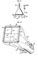
- a CRT 100 is arranged in a standard manner such that an electron beam from an electron gun (not shown) impinges upon a phosphorescent coating on the inner surface of the display screen or face 101 of the CRT in a raster scan pattern, sequentially line by line from top to bottom. As the electrons high the phosphorescent inner surface, the screen 101 of CRT 100 glows. Illustratively, screen 101 and display areas 102 of CRT 100 are shown as having a rectangular shape herein.
- the screen 101 of CRT 100 is divided into two display areas 102 and 103.
- a bezel covers all but the display area 102 of the screen 101 of CRT 100.
- Display area 102 is the image display area which typically uses a medium-short persistence phosphor.
- a coordinate display area 103 is used to generate the light beams or signals used in detecting the X, Y coordinates when the image area 102 is touched.
- Coordinate display area 103 may use a short persistence phosphor whose decay time is less than the image pel time.
- coordinate display area 103 is further divided into areas or sections 104 and 105.
- Section 104 generates the row of discrete light sources or video dots 106 used in detecting the X coordinate of display area 102.
- the video signal is unblanked and a row of dots 106 is generated in section 104, where the number of dots may be equal to the number of picture elements (pels)/line in the image display area 102.
- Section 105 generates the discrete light signals used in detecting the Y coordinate of display area 102.
- the video signal is unblanked for about one pel period and a column of video dots 107 is generated in section 105, where one dot may be generated for each horizonatal line in the image display area 102.
- each pel in the image display area 102 is defined by a dot of light (one per pel) determining its X coordinate and a dot of light (one per scan line) determining its Y coordinate.
- display area 104 may use a short persistence phosphor, once a dot in row 106 is illuminated by the scanning electron beam, it is likely that the time constant of the phosphor persistence will cause that dot to glow for a while after the scanning electron beam has moved to the next dot in row 106. Since the ability to detect when a particular area of the display has been touched is enhanced when only one dot at a time is illuminated, the arrangements of dots shown in FIG. 2 would improve detection.
- Dot arrangement 201 uses dots which alternate between field 1 (f1) line n and field 2 (f2) line n.
- the light dots for odd pels (P1, P3, P5, etc.) are generated first during field f1 line n, while the light dots for even pels (P2, P4, P6, etc.) are generated during field f2 line n.
- the elapsed time between the illumination dots on the same line, e.g., pel P3 and pel P1 is two pel times rather then one pel time, when all the dots are on the same frame and line number.
- FIG. 202 Shown in 202 is another possible dot arrangement where the dot for every pel in the display, P1 - PM, is generated alternately on frame F1 field f1 line n, frame F1 field f2 line n, frame F2 field f1 line n + 1 and frame F2 field f2 line n + 1. Since there are four pel times between dots on the same frame and line, there is an effective reduction of the persistence time constant of the phosphor by about a factor of four.
- FIG. 3 shows a top view of the optical apparatus and photodetector layout for detecting the Y coordinate of the image display area 102.
- the layout for detecting the X coordinate is identical except that it is rotated 90 degrees with respect to the layout for the Y coordinate.
- a front surface mounted light deflector or mirror 301 is placed in front of the column of Y coordinate dots 107 and angled to deflect the light beams 302 generated by dots 107 across display area 102 of CRT 100 as illustrated by the dashed lines 303.
- the resulting row beams of light, 303, crossing the screen of CRT 100 are collected and focused. 305, by a parabolic reflector 304 or equivalent optical apparatus onto the Y coordinate photodetector 306.
- This optical apparatus layout provides a means for generating rows of scanning light beams across the image display area 102 of C RT 100, one for each horizontal scan line in the displayed picture.
- the disclosed apparatus can be arranged to deflect the light beams across any predetermined part of the image display area 102.
- FIG. 4 is a perspective view of CRT 100 with mirror 301, deflector 304 and photodetector 306. Also shown in FIG. 4 is an equivalent optical apparatus layout, including front surface mirror 401 for deflecting light beams generated by the row of X coordinate dots, parabolic reflector 402, and photodetector 403 for detecting the columns of scanning light beams which cross display area 102 . It is contemplated that other light collecting means, e.g., multiple photodetector means, could be appropriately positioned to obviate the need for parabolic reflectors 304 and 402.
- a finger or pointer object e.g., 307
- the resulting interruption of the beams of light e.g., 303 and 403, at the selected location X1, Y1 is detected at photodetectors 306 and 403.
- This interruption of light is processed by circuitry, discussed in subsequent paragraphs, to determine the X and Y coordinates of the pel selected on the display (or the centroid if the pointer covered multiple pels on the display) by pointer 307.
- the processing circuitry requires the scan timing signals of CRT 100 to determine the exact row(s) and column(s) of light beams interrupted by pointer 307..
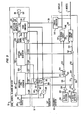
- FIG. 5 illustrates suitable control and signal processing circuits. These circuits include sync, address, blanking and video circuits 50: dot generator 51; and coordinate detector 52. Illustratively, in the following description the CR T is assumed to operate at the standard television interlaced field format.
- the standard system clock 500 generates a clock signal at the pel rate, which is applied over lead 501 to horizontal sync generator 502, AND gate 503, and divide by two counter circuit 504.
- Horizontal sync generator 502 and vertical sync generator 505 utilize well known counting circuits to generate X and Y coordinate address information as well as the standard synchronization signals used for cameras and video display devices.
- Lead 506 supplies vertical sync generator 505 with a 2X horizontal pulse from the horizontal sync generator 502 to provide the arrangement or digitizer system with standard 2:1 interlace.
- Lead 507 from horizontal sync generator 502 and lead 508 from vertical sync generator 505 supply well known deflection amplifiers 509 with standard drive pulses to generate scan or sweep signals for CRT 100.
- the horizontal sweep signals on lead 510 and the vertical sweep signal 511 are applied to the corresponding deflection yokes of CRT 100.
- Video combiner 512 receives standard baseband video signals on lead 513, standard vertical blanking signals on lead 514, standard horizontal blanking signals on lead 515, the inventive row of dot signals on lead 516, the inventive column of dot signals on lead 517 and a cursor signal on lead 518. These signals are combined, using standard techniques, to generate a composite video signal on lead 519 which is applied to CRT 100. These combined signals cause CRT 100 to display the usual video signal in image display area 102, and to display a row of dots in area 104 and a column of dots in area 105 of the conventionally blanked areas of the screen.
- the displayed row of dots (i.e., 201 of FIG. 2) is generated from signals from dot generator 51.
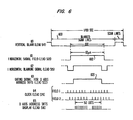
- vertical sync generator 505 selects one horizontal scan line period per field, 601 of waveform 60, near the end of its normal blanking period, 600, and outputs on lead 52Q_ to one input of AND gate 521 a positive pulse, waveform 61, for the 63 p sec duration of that horizontal scan line period.
- Horizontal sync generator 502 supplies its blanking signal (waveform 62), which is high during the active display time 602, on lead 515 to the other input of AND gate 521.
- This signal gates the row of dot signals used in determining the X coordinate or horizontal address.
- This input 522 in combination with the divided by two clock signal, waveform 64 on lead 524, causes AND gate 523 to output one line of signals at one-half the pel rate on lead 516.
- waveform 64 the signals for one-half of the row of dots are generated in each field, F1 and F 2, for a total of 512 dots/frame for a standard broadcast video picture. Obviously, if a half horizontal detection resolution is desired, such as shown in 106 of FIG. 1, only the field 1 or field 2 signal of waveform 64 need be used.
- Video combiner 512 generates the signals which result in a display of a row of dots on the screen of the CRT.
- dot generator 51 can be arranged to provide dots at less than the pel rate.
- the displayed column of dots (i.e., 107 of F I G. 1) is also generated from signals from dot generator 51.
- horizontal sync generator 502 With joint reference to FIG. 5 and the waveforms of FIG. 7, horizontal sync generator 502 generates, in a standard manner, a signal 526, which is less than the width of two clock periods, waveform 71, at the trailing edge of the normally blanked segment of the horizontal scan signals, 701 of waveform 70.
- This signal is applied on lead 526 to AND gate 503.
- This signal in combination with the clock pulses 501, waveform 72, on lead 501 causes AND gate 503 to generate a positive pulse signal on lead 517 which is one pel time wide each horizontal scan line period of each frame as shown by waveform 73.
- the signal on lead 517 is applied to video combiner 512 which generates a signal to produce a column of dots, one per scan line on the CRT. This column of dots provides Y coordinate or vertical address information.
- the signal on lead 517 is also applied to AND gate 534 in the detector circuit 52.
- dot generator 51 can be arranged to provide fewer than one dot per horizontal scan line (e.g., one dot for every two scan lines, etc.).
- Coordinate detector 52 determines both the X and Y coordinates of the display area touched by a finger or pointer. With joint reference to FIG. 4, FIG. 5 and the waveforms of FIG. 8, assume that the determination of the X-axis touch coordinate is desired.
- the X axis photodetector 403 generates on lead 528 a string of logic 1s, one for each pel of a horizontal scan line of a frame, waveform 80, if the light beam path across the face or screen of CRT 100 is not interrupted. When the light path is interrupted, the absence of light on X-axis photodetector 403 causes one or more logic Os to appear on output lead 528 (depending on the size of the point or finger, 307 of FIG. 3).
- the logic Os on lead 528 are converted to logic 1s by inverter 529 and appear as waveform 81 on output lead 530.
- Lead 530 is ANDED with row dot signals on lead 516, waveform 82, to produce logic 1s, waveform 83; on lead 543 of AND gate 525.
- the logic 1 signals on lead 543 are gated by AND gate 544 to lead 529 using the horizontal blanking period signal on lead 527.
- Lead 529 applies the logic 1s, each representing an X coordinate, X1, or pointer 307, to the input of the X averaging circuit 530, which determines or calculates the average X coordinate or address.
- the average or centroid of the X address (X1 of waveform 83) is calculated because the size of pointer 307 will probably block the light coming from several dots.
- the X averaging circuit 530 is reset once each frame time by a pulse arriving on lead 531 from vertical sync generator 505.
- Y-axis touch coordinate determination and calculation are processed in the same manner as the X-axis address.
- Y-axis photodetector 306 generates on lead 531 a string of logic ls, one for each horizontal scan line, as long as light is received and, accordingly, generates one or more logic Os when the light is interrupted.
- Output 531 from Y-axis photodetector 403 is inverted in inverter 532 and gated with the column dot signals on lead 517 in AND gate 534.
- the output 535 of AND gate 534 is gated in AND gate 537 with a vertical blanking interval signal on lead 536.
- the output 538 of AND gate 537 is applied to Y averaging circuit 539 which determines or calculates the average Y coordinate address.
- the Y averaging circuit 539 is reset once each frame from a signal on lead 531 from vertical sync generator 505.
- the output of X averaging circuit 530 on lead 540 and the output of Y averaging circuit 539 on lead 541 are applied to a well known cursor generator 542, which generates a signal on lead 518 which is combined with other signals by the video combiner 512 to place a video dot or mark in the active display area 102 on CRT 100 to indicate the X1, Y1 coordinate location to which pointer 307 pointed.
- the X and Y coordinate or address signals on leads 540 and 541, respectively, may also be used by other circuitry in another part of the video system (not shown) to select a pel or parts of the picture for special processing.
Abstract
Description
- This invention relates to display screen touch position detection apparatus.
- Modern video displays, such as interactive graphics stations, enable the operator or user to perform certain operations by selecting functions from a displayed menu of possible choices. At an interactive graphics station, user controlled functions typically involve selecting a system operating capability from a menu and then selecting the locaion on the display image where the operation is to be carried out. While the selection of the operation from the menu typically requires only a low resolution touch detection apparaus, the selection of the location on the image at which to perform the operation often requires a high resolution touch detector or digitizer. Existing digitizers which allow the user to select the X and Y coordinates either use high resolution off-the-screen digitizers or low resolution on-the-screen devices. The off-the-screen digitzer is undesirable since the user cannot work directly with the displayed image. The on-the-screen devices typically are touch sensitive devices where the resolution is limited by the resolution of the touch detection screen matrix or the pointer or finger used to touch the screen. What is desired is an on-the-screen device having the high resolution of off-the-screen digitizers.
- According to this invention display screen touch position detection apparatus includes means for providing a plurality of light signals for propagation across a display area of the display device, and means responsive to selective interruption of the propagating light signals for detecting the position of the interrupting agency.
- In one embodiment of the invention, selected line scanning signals of the video display cathode-ray tube (CRT) are unblanked during the vertical blanking period and a row of picture element (pel) sized dots of light are generated. During the normal horizontal blanking period a column of pel-sized light dots is formed by unblanking the video signal and generating a column of pel sized dots, one for each scan line of the display. The row and column of pel-sized light dots are reflected by mirrors across the face of the display forming, respectively, an X and Y coordinate matrix of light beams which are then reflected, respectively, to an X position and Y position detector. Detector circuitry detects and calculates the X and Y coordinate location of the centroid of a pointer or a finger which interrupts the light beams and outputs an appropriate address signal in response thereto. A cursor generator provides a cursor on the CRT display at the X and Y coordinates of the touch location.
- The invention will now be described by way of example with reference to the accompanying drawings in which:
- FIG. 1 shows a CRT for use in describing the present invention;
- FIG. 2 shows various dot generating arrangements for use in the present invention;
- FIG. 3 shows a top view of apparatus for providing optical reflection and collection of the light beams or signals generated by the CRT of FIG. 1;
- FIG. 4 shows a perspective view of optical apparatus in assocation with the CRT of FIG. 1;
- FIG. 5 shows a video control and signal processing circuit;
- FIG. 6 shows waveforms useful in describing the generation of a row of video dots used for horizontal address detection;
- FIG. 7 shows waveforms useful in describing the generation of a column of video dots used for vertical address detection; and
- FIG. 8 shows waveforms useful in describing the detection of interruption of light beams by the video control and signal processing circuit of FIG. 5.
- Referring now to FIG. 1, a
CRT 100 is arranged in a standard manner such that an electron beam from an electron gun (not shown) impinges upon a phosphorescent coating on the inner surface of the display screen orface 101 of the CRT in a raster scan pattern, sequentially line by line from top to bottom. As the electrons high the phosphorescent inner surface, thescreen 101 ofCRT 100 glows. Illustratively,screen 101 anddisplay areas 102 of CRT 100 are shown as having a rectangular shape herein. - The
screen 101 of CRT 100 is divided into twodisplay areas display area 102 of thescreen 101 of CRT 100.Display area 102 is the image display area which typically uses a medium-short persistence phosphor. In this example of the invention, acoordinate display area 103 is used to generate the light beams or signals used in detecting the X, Y coordinates when theimage area 102 is touched.Coordinate display area 103 may use a short persistence phosphor whose decay time is less than the image pel time. - Illustratively,
coordinate display area 103 is further divided into areas orsections Section 104 generates the row of discrete light sources orvideo dots 106 used in detecting the X coordinate ofdisplay area 102. During the normal vertical blanking period, the video signal is unblanked and a row ofdots 106 is generated insection 104, where the number of dots may be equal to the number of picture elements (pels)/line in theimage display area 102.Section 105 generates the discrete light signals used in detecting the Y coordinate ofdisplay area 102. During the normal horizontal blanking period, the video signal is unblanked for about one pel period and a column ofvideo dots 107 is generated insection 105, where one dot may be generated for each horizonatal line in theimage display area 102. - As shown in FIG. 1, when a resolution of less than 1 pel is desired, the number of dots in either
row 106 andcolumn 107 is less than the number of pels per line or number of video scan lines, respectively. However, when a resolution of one pel is desired, each pel in theimage display area 102 is defined by a dot of light (one per pel) determining its X coordinate and a dot of light (one per scan line) determining its Y coordinate. - Even though
display area 104 may use a short persistence phosphor, once a dot inrow 106 is illuminated by the scanning electron beam, it is likely that the time constant of the phosphor persistence will cause that dot to glow for a while after the scanning electron beam has moved to the next dot inrow 106. Since the ability to detect when a particular area of the display has been touched is enhanced when only one dot at a time is illuminated, the arrangements of dots shown in FIG. 2 would improve detection. - Shown in FIG. 2 are two dot arrangements, 201 and 202, for
section 104 using 2:1 interlaced raster scanning.Dot arrangement 201 uses dots which alternate between field 1 (f1) line n and field 2 (f2) line n. In 201, the light dots for odd pels (P1, P3, P5, etc.) are generated first during field f1 line n, while the light dots for even pels (P2, P4, P6, etc.) are generated during field f2 line n. Thus, the elapsed time between the illumination dots on the same line, e.g., pel P3 and pel P1 is two pel times rather then one pel time, when all the dots are on the same frame and line number. Hence, the effects of the persistence of the phosphor on touch detection accuracy is reduced. The result is that touch detection accuracy is enhanced or that the same touch detection accuracy can be had with phosphor having a time constant twice as long. Shown in 202 is another possible dot arrangement where the dot for every pel in the display, P1 - PM, is generated alternately on frame F1 field f1 line n, frame F1 field f2 line n, frame F2 field f1 line n + 1 and frame F2 field f2 line n + 1. Since there are four pel times between dots on the same frame and line, there is an effective reduction of the persistence time constant of the phosphor by about a factor of four. Obviously, the techniques described above can be utilized to generate lines of dots on successive frames rather than on successive fields of the display. Note, since there is a scan line time period between the generation of each dot in the column ofdots 107, the utilization of dot arrangements similar to those discussed above are typically not required forsection 105. - FIG. 3 shows a top view of the optical apparatus and photodetector layout for detecting the Y coordinate of the
image display area 102. The layout for detecting the X coordinate is identical except that it is rotated 90 degrees with respect to the layout for the Y coordinate. - In one embodiment, a front surface mounted light deflector or
mirror 301 is placed in front of the column of Ycoordinate dots 107 and angled to deflect thelight beams 302 generated bydots 107 acrossdisplay area 102 ofCRT 100 as illustrated by thedashed lines 303. The resulting row beams of light, 303, crossing the screen ofCRT 100 are collected and focused. 305, by aparabolic reflector 304 or equivalent optical apparatus onto theY coordinate photodetector 306. This optical apparatus layout provides a means for generating rows of scanning light beams across theimage display area 102 of CRT 100, one for each horizontal scan line in the displayed picture. Obviously, if desired the disclosed apparatus can be arranged to deflect the light beams across any predetermined part of theimage display area 102. - FIG. 4 is a perspective view of
CRT 100 withmirror 301,deflector 304 andphotodetector 306. Also shown in FIG. 4 is an equivalent optical apparatus layout, includingfront surface mirror 401 for deflecting light beams generated by the row of X coordinate dots,parabolic reflector 402, andphotodetector 403 for detecting the columns of scanning light beams which cross display area 102. It is contemplated that other light collecting means, e.g., multiple photodetector means, could be appropriately positioned to obviate the need forparabolic reflectors - With joint reference to FIG. 3 and 4, if a finger or pointer object, e.g., 307, is used to select or point to a location X1, Y1 on
display 102, the resulting interruption of the beams of light, e.g., 303 and 403, at the selected location X1, Y1 is detected atphotodetectors pointer 307. Note, since all the row scanning beams of light are focused 404 onto onephotodetector 306 and all the column scanning beams of light are focused 405 onto onephotodetector 403, the processing circuitry requires the scan timing signals ofCRT 100 to determine the exact row(s) and column(s) of light beams interrupted bypointer 307.. - FIG. 5. illustrates suitable control and signal processing circuits. These circuits include sync, address, blanking and video circuits 50:
dot generator 51; and coordinatedetector 52. Illustratively, in the following description the CRT is assumed to operate at the standard television interlaced field format. - In
video circuit 50, thestandard system clock 500 generates a clock signal at the pel rate, which is applied overlead 501 to horizontal sync generator 502, ANDgate 503, and divide by twocounter circuit 504. - Horizontal sync generator 502 and
vertical sync generator 505 utilize well known counting circuits to generate X and Y coordinate address information as well as the standard synchronization signals used for cameras and video display devices. Lead 506 suppliesvertical sync generator 505 with a 2X horizontal pulse from the horizontal sync generator 502 to provide the arrangement or digitizer system with standard 2:1 interlace. Lead 507 from horizontal sync generator 502 and lead 508 fromvertical sync generator 505 supply well knowndeflection amplifiers 509 with standard drive pulses to generate scan or sweep signals forCRT 100. The horizontal sweep signals onlead 510 and thevertical sweep signal 511 are applied to the corresponding deflection yokes ofCRT 100. -
Video combiner 512 receives standard baseband video signals onlead 513, standard vertical blanking signals onlead 514, standard horizontal blanking signals onlead 515, the inventive row of dot signals onlead 516, the inventive column of dot signals onlead 517 and a cursor signal onlead 518. These signals are combined, using standard techniques, to generate a composite video signal onlead 519 which is applied toCRT 100. These combined signals causeCRT 100 to display the usual video signal inimage display area 102, and to display a row of dots inarea 104 and a column of dots inarea 105 of the conventionally blanked areas of the screen. - The displayed row of dots (i.e., 201 of FIG. 2) is generated from signals from
dot generator 51. With joint reference to FIG. 5 and 6,vertical sync generator 505 selects one horizontal scan line period per field, 601 ofwaveform 60, near the end of its normal blanking period, 600, and outputs on lead 52Q_ to one input of AND gate 521 a positive pulse,waveform 61, for the 63 p sec duration of that horizontal scan line period. - Horizontal sync generator 502 supplies its blanking signal (waveform 62), which is high during the
active display time 602, onlead 515 to the other input of ANDgate 521. The output, lead 522, of ANDgate 521 which is high during theactive display time 603 of one horizontal scan period of a field,waveform 63, is applied to ANDgate 523. This signal gates the row of dot signals used in determining the X coordinate or horizontal address. Thisinput 522 in combination with the divided by two clock signal,waveform 64 onlead 524, causes ANDgate 523 to output one line of signals at one-half the pel rate onlead 516. As shown inwaveform 64, the signals for one-half of the row of dots are generated in each field, F1 and F2, for a total of 512 dots/frame for a standard broadcast video picture. Obviously, if a half horizontal detection resolution is desired, such as shown in 106 of FIG. 1, only thefield 1 orfield 2 signal ofwaveform 64 need be used. - The signals for 2 fields on
lead 516, as shown inwaveform 65, are applied tovideo combiner 512 and ANDgate 525.Video combiner 512 generates the signals which result in a display of a row of dots on the screen of the CRT. As noted, when a lower touch detection resolution is desired,dot generator 51 can be arranged to provide dots at less than the pel rate. - The displayed column of dots (i.e., 107 of FIG. 1) is also generated from signals from
dot generator 51. With joint reference to FIG. 5 and the waveforms of FIG. 7, horizontal sync generator 502 generates, in a standard manner, asignal 526, which is less than the width of two clock periods, waveform 71, at the trailing edge of the normally blanked segment of the horizontal scan signals, 701 ofwaveform 70. This signal is applied onlead 526 to ANDgate 503. This signal in combination with theclock pulses 501,waveform 72, onlead 501 causes ANDgate 503 to generate a positive pulse signal onlead 517 which is one pel time wide each horizontal scan line period of each frame as shown bywaveform 73. The signal onlead 517 is applied tovideo combiner 512 which generates a signal to produce a column of dots, one per scan line on the CRT. This column of dots provides Y coordinate or vertical address information. The signal onlead 517 is also applied to ANDgate 534 in thedetector circuit 52. Obviously, if a lower touch detection resolution is desired,dot generator 51 can be arranged to provide fewer than one dot per horizontal scan line (e.g., one dot for every two scan lines, etc.). - Coordinate
detector 52 determines both the X and Y coordinates of the display area touched by a finger or pointer. With joint reference to FIG. 4, FIG. 5 and the waveforms of FIG. 8, assume that the determination of the X-axis touch coordinate is desired. TheX axis photodetector 403 generates on lead 528 a string of logic 1s, one for each pel of a horizontal scan line of a frame,waveform 80, if the light beam path across the face or screen ofCRT 100 is not interrupted. When the light path is interrupted, the absence of light onX-axis photodetector 403 causes one or more logic Os to appear on output lead 528 (depending on the size of the point or finger, 307 of FIG. 3). The logic Os onlead 528 are converted to logic 1s byinverter 529 and appear aswaveform 81 onoutput lead 530.Lead 530 is ANDED with row dot signals onlead 516,waveform 82, to produce logic 1s,waveform 83; onlead 543 of ANDgate 525. Thelogic 1 signals onlead 543 are gated by ANDgate 544 to lead 529 using the horizontal blanking period signal onlead 527.Lead 529 applies the logic 1s, each representing an X coordinate, X1, orpointer 307, to the input of theX averaging circuit 530, which determines or calculates the average X coordinate or address. The average or centroid of the X address (X1 of waveform 83) is calculated because the size ofpointer 307 will probably block the light coming from several dots. TheX averaging circuit 530 is reset once each frame time by a pulse arriving onlead 531 fromvertical sync generator 505. - The Y-axis touch coordinate determination and calculation are processed in the same manner as the X-axis address. Thus, Y-
axis photodetector 306 generates on lead 531 a string of logic ls, one for each horizontal scan line, as long as light is received and, accordingly, generates one or more logic Os when the light is interrupted.Output 531 from Y-axis photodetector 403 is inverted ininverter 532 and gated with the column dot signals onlead 517 in ANDgate 534. Theoutput 535 of ANDgate 534 is gated in ANDgate 537 with a vertical blanking interval signal onlead 536. Theoutput 538 of ANDgate 537 is applied toY averaging circuit 539 which determines or calculates the average Y coordinate address. TheY averaging circuit 539 is reset once each frame from a signal onlead 531 fromvertical sync generator 505. - The output of
X averaging circuit 530 onlead 540 and the output ofY averaging circuit 539 onlead 541 are applied to a well knowncursor generator 542, which generates a signal onlead 518 which is combined with other signals by thevideo combiner 512 to place a video dot or mark in theactive display area 102 onCRT 100 to indicate the X1, Y1 coordinate location to whichpointer 307 pointed. The X and Y coordinate or address signals onleads - Variations will occur to those skilled in the art. For example, equivalent components and circuitry are well known which can replace the apparatus or devices shown and described herein. Thus, while the present invention has been described for use with a CRT, it is contemplated that the invention can be applied to other video displays by implementing an equivalent coordinate display area.
Claims (5)
Applications Claiming Priority (2)
| Application Number | Priority Date | Filing Date | Title |
|---|---|---|---|
| US06/523,000 US4621257A (en) | 1983-08-15 | 1983-08-15 | Video display touch detection digitizer |
| US523000 | 1983-08-15 |
Publications (3)
| Publication Number | Publication Date |
|---|---|
| EP0137619A2 true EP0137619A2 (en) | 1985-04-17 |
| EP0137619A3 EP0137619A3 (en) | 1985-07-31 |
| EP0137619B1 EP0137619B1 (en) | 1988-11-30 |
Family
ID=24083252
Family Applications (1)
| Application Number | Title | Priority Date | Filing Date |
|---|---|---|---|
| EP84305343A Expired EP0137619B1 (en) | 1983-08-15 | 1984-08-07 | Display screen touch position detection apparatus |
Country Status (9)
| Country | Link |
|---|---|
| US (1) | US4621257A (en) |
| EP (1) | EP0137619B1 (en) |
| JP (1) | JPS6065328A (en) |
| KR (1) | KR920009766B1 (en) |
| CA (1) | CA1233922A (en) |
| DE (1) | DE3475445D1 (en) |
| ES (1) | ES8507306A1 (en) |
| HK (1) | HK4790A (en) |
| SG (1) | SG15489G (en) |
Cited By (2)
| Publication number | Priority date | Publication date | Assignee | Title |
|---|---|---|---|---|
| FR2593303A1 (en) * | 1986-01-23 | 1987-07-24 | Dassault Electronique | Touch screen emulating a light pen |
| EP0365232A2 (en) * | 1988-10-17 | 1990-04-25 | Tektronix Inc. | Integrated liquid crystal display and optical touch panel |
Families Citing this family (14)
| Publication number | Priority date | Publication date | Assignee | Title |
|---|---|---|---|---|
| US4821029A (en) * | 1984-04-26 | 1989-04-11 | Microtouch Systems, Inc. | Touch screen computer-operated video display process and apparatus |
| JPH0337070Y2 (en) * | 1984-10-31 | 1991-08-06 | ||
| JPS61202218A (en) * | 1985-03-06 | 1986-09-08 | Canon Inc | Input and output device |
| US4777482A (en) * | 1985-08-08 | 1988-10-11 | Honeywell Inc. | Finger-touch coordinate input apparatus including a supply of air for dust removal |
| JPH02176819A (en) * | 1988-08-15 | 1990-07-10 | Fujitsu Ltd | Optical coordinate input device |
| US5036964A (en) * | 1990-03-28 | 1991-08-06 | Dana Corporation | Armature assembly for an electromagnetic coupling |
| US5272469A (en) * | 1991-07-01 | 1993-12-21 | Ncr Corporation | Process for mapping high resolution data into a lower resolution depiction |
| US5422494A (en) * | 1992-10-16 | 1995-06-06 | The Scott Fetzer Company | Barrier transmission apparatus |
| US6476798B1 (en) | 1994-08-22 | 2002-11-05 | International Game Technology | Reduced noise touch screen apparatus and method |
| US5764223A (en) * | 1995-06-07 | 1998-06-09 | International Business Machines Corporation | Touch-screen input device using the monitor as a light source operating at an intermediate frequency |
| US6493575B1 (en) | 1998-06-04 | 2002-12-10 | Randy J. Kesten | Fluoroscopic tracking enhanced intraventricular catheter system |
| US6947786B2 (en) | 2002-02-28 | 2005-09-20 | Surgical Navigation Technologies, Inc. | Method and apparatus for perspective inversion |
| JP2008523424A (en) * | 2004-12-09 | 2008-07-03 | アールピーオー プロプライエタリー リミテッド | Optical power distribution device |
| TWI506606B (en) * | 2010-11-05 | 2015-11-01 | Novatek Microelectronics Corp | Touch controller for touch-sensing display panel and driving method thereof |
Citations (2)
| Publication number | Priority date | Publication date | Assignee | Title |
|---|---|---|---|---|
| US4305071A (en) * | 1980-04-16 | 1981-12-08 | Bell Telephone Laboratories, Incorporated | Touch sensitive screen signal detection arrangement |
| FR2486267A1 (en) * | 1980-07-04 | 1982-01-08 | Hewlett Packard France Sa | SENSOR MATRIX FOR DISPLAY SCREENS |
Family Cites Families (17)
| Publication number | Priority date | Publication date | Assignee | Title |
|---|---|---|---|---|
| US3673327A (en) * | 1970-11-02 | 1972-06-27 | Atomic Energy Commission | Touch actuable data input panel assembly |
| US3846826A (en) * | 1971-08-12 | 1974-11-05 | R Mueller | Direct television drawing and image manipulating system |
| US3775560A (en) * | 1972-02-28 | 1973-11-27 | Univ Illinois | Infrared light beam x-y position encoder for display devices |
| US3764813A (en) * | 1972-04-12 | 1973-10-09 | Bell Telephone Labor Inc | Coordinate detection system |
| JPS5517420B2 (en) * | 1974-06-10 | 1980-05-12 | ||
| JPS5129060A (en) * | 1974-09-03 | 1976-03-11 | Univ Australian | |
| DE2654464A1 (en) * | 1976-12-01 | 1978-06-08 | Sick Optik Elektronik Erwin | PHOTOELECTRIC LIGHT RECEIVING ARRANGEMENT |
| JPS5417507A (en) * | 1977-07-11 | 1979-02-08 | Toshiba Corp | Electromagnetic pump |
| US4205304A (en) * | 1977-09-22 | 1980-05-27 | General Electric Company | Two dimensional light beam selection system |
| CA1109539A (en) * | 1978-04-05 | 1981-09-22 | Her Majesty The Queen, In Right Of Canada, As Represented By The Ministe R Of Communications | Touch sensitive computer input device |
| US4177354A (en) * | 1978-04-17 | 1979-12-04 | Bell Telephone Laboratories, Incorporated | Graphic communications apparatus |
| JPS55110330A (en) * | 1979-02-16 | 1980-08-25 | Mitsubishi Electric Corp | Information input unit |
| US4346376A (en) * | 1980-04-16 | 1982-08-24 | Bell Telephone Laboratories, Incorporated | Touch position sensitive surface |
| CA1185383A (en) * | 1980-04-16 | 1985-04-09 | Leonard R. Kasday | Touch position sensitive device |
| JPS5851335A (en) * | 1981-09-22 | 1983-03-26 | Advance:Kk | Detection system for coordinate position information |
| US4459476A (en) * | 1982-01-19 | 1984-07-10 | Zenith Radio Corporation | Co-ordinate detection system |
| US4517559A (en) * | 1982-08-12 | 1985-05-14 | Zenith Electronics Corporation | Optical gating scheme for display touch control |
-
1983
- 1983-08-15 US US06/523,000 patent/US4621257A/en not_active Expired - Lifetime
-
1984
- 1984-06-28 CA CA000457644A patent/CA1233922A/en not_active Expired
- 1984-08-07 DE DE8484305343T patent/DE3475445D1/en not_active Expired
- 1984-08-07 EP EP84305343A patent/EP0137619B1/en not_active Expired
- 1984-08-14 ES ES535165A patent/ES8507306A1/en not_active Expired
- 1984-08-14 KR KR1019840004897A patent/KR920009766B1/en not_active IP Right Cessation
- 1984-08-15 JP JP59169480A patent/JPS6065328A/en active Granted
-
1989
- 1989-03-09 SG SG154/89A patent/SG15489G/en unknown
-
1990
- 1990-01-18 HK HK47/90A patent/HK4790A/en not_active IP Right Cessation
Patent Citations (2)
| Publication number | Priority date | Publication date | Assignee | Title |
|---|---|---|---|---|
| US4305071A (en) * | 1980-04-16 | 1981-12-08 | Bell Telephone Laboratories, Incorporated | Touch sensitive screen signal detection arrangement |
| FR2486267A1 (en) * | 1980-07-04 | 1982-01-08 | Hewlett Packard France Sa | SENSOR MATRIX FOR DISPLAY SCREENS |
Non-Patent Citations (2)
| Title |
|---|
| IBM TECHNICAL DISCLOSURE BULLETIN, vol. 24, no. 6, November 1981, pages 2732-2733, New York, US; R.H. HARRIS: "Optical overlay input device for a cathode ray tube" * |
| RADIO FERNSEHEN ELEKTRONIK, vol. 32, no. 3, March 1983, pages 147-149, Ost-Berlin, DD; K. ENGELMANN: "Kursorpositionierung mit Lichtstift" * |
Cited By (3)
| Publication number | Priority date | Publication date | Assignee | Title |
|---|---|---|---|---|
| FR2593303A1 (en) * | 1986-01-23 | 1987-07-24 | Dassault Electronique | Touch screen emulating a light pen |
| EP0365232A2 (en) * | 1988-10-17 | 1990-04-25 | Tektronix Inc. | Integrated liquid crystal display and optical touch panel |
| EP0365232A3 (en) * | 1988-10-17 | 1990-06-13 | Tektronix Inc. | Integrated liquid crystal display and optical touch panel |
Also Published As
| Publication number | Publication date |
|---|---|
| EP0137619B1 (en) | 1988-11-30 |
| DE3475445D1 (en) | 1989-01-05 |
| US4621257A (en) | 1986-11-04 |
| CA1233922A (en) | 1988-03-08 |
| EP0137619A3 (en) | 1985-07-31 |
| SG15489G (en) | 1989-06-09 |
| HK4790A (en) | 1990-01-25 |
| KR850002165A (en) | 1985-05-06 |
| ES535165A0 (en) | 1985-09-01 |
| JPS6065328A (en) | 1985-04-15 |
| ES8507306A1 (en) | 1985-09-01 |
| JPH0142006B2 (en) | 1989-09-08 |
| KR920009766B1 (en) | 1992-10-22 |
Similar Documents
| Publication | Publication Date | Title |
|---|---|---|
| EP0137619B1 (en) | Display screen touch position detection apparatus | |
| US4459476A (en) | Co-ordinate detection system | |
| US6492633B2 (en) | Optical scanning-type touch panel | |
| US4517559A (en) | Optical gating scheme for display touch control | |
| US4247767A (en) | Touch sensitive computer input device | |
| JPS6244653B2 (en) | ||
| US4634970A (en) | Digital waveform processing oscilloscope with distributed data multiple plane display system | |
| JP3121715B2 (en) | Information display device | |
| US5179368A (en) | Method and apparatus for interfacing computer light pens | |
| CA1071782A (en) | Iterative coordinate data approximation system for photoemissive pixel pattern displays | |
| US4929935A (en) | Apparatus for aligning raster scanned image to touch panel | |
| EP0381426A2 (en) | Apparatus for determining the position of a light pen on a display device | |
| EP0144088A1 (en) | Pointer apparatus for display devices | |
| US4335380A (en) | Multi-beam raster scan display monitor | |
| JP3109392B2 (en) | Image processing device | |
| SU1501027A1 (en) | Graphic information input device | |
| US4146878A (en) | Video display apparatus display modification | |
| JPS59195734A (en) | Light pen input device | |
| SU739585A1 (en) | Device for displaying vectors on the screen of crt | |
| SU651380A1 (en) | Arrangement for displaying information on crt screen | |
| SU982074A1 (en) | Device for determining coordinates point image on crt screen | |
| SU807265A1 (en) | Device for displaying information on crt screen | |
| SU1034054A2 (en) | Graphic data reading device | |
| SU1304055A1 (en) | Device for displaying information on screen of cathode-ray tube | |
| JPH09244791A (en) | Information input device, display and information input method |
Legal Events
| Date | Code | Title | Description |
|---|---|---|---|
| PUAI | Public reference made under article 153(3) epc to a published international application that has entered the european phase |
Free format text: ORIGINAL CODE: 0009012 |
|
| AK | Designated contracting states |
Designated state(s): BE DE FR GB IT NL SE |
|
| PUAL | Search report despatched |
Free format text: ORIGINAL CODE: 0009013 |
|
| AK | Designated contracting states |
Designated state(s): BE DE FR GB IT NL SE |
|
| 17P | Request for examination filed |
Effective date: 19851217 |
|
| 17Q | First examination report despatched |
Effective date: 19870115 |
|
| GRAA | (expected) grant |
Free format text: ORIGINAL CODE: 0009210 |
|
| AK | Designated contracting states |
Kind code of ref document: B1 Designated state(s): BE DE FR GB IT NL SE |
|
| REF | Corresponds to: |
Ref document number: 3475445 Country of ref document: DE Date of ref document: 19890105 |
|
| ITF | It: translation for a ep patent filed |
Owner name: MODIANO & ASSOCIATI S.R.L. |
|
| ET | Fr: translation filed | ||
| PLBE | No opposition filed within time limit |
Free format text: ORIGINAL CODE: 0009261 |
|
| STAA | Information on the status of an ep patent application or granted ep patent |
Free format text: STATUS: NO OPPOSITION FILED WITHIN TIME LIMIT |
|
| 26N | No opposition filed | ||
| ITTA | It: last paid annual fee | ||
| EAL | Se: european patent in force in sweden |
Ref document number: 84305343.0 |
|
| PGFP | Annual fee paid to national office [announced via postgrant information from national office to epo] |
Ref country code: FR Payment date: 19980619 Year of fee payment: 15 |
|
| PGFP | Annual fee paid to national office [announced via postgrant information from national office to epo] |
Ref country code: SE Payment date: 19980624 Year of fee payment: 15 Ref country code: GB Payment date: 19980624 Year of fee payment: 15 |
|
| PGFP | Annual fee paid to national office [announced via postgrant information from national office to epo] |
Ref country code: BE Payment date: 19980701 Year of fee payment: 15 |
|
| PGFP | Annual fee paid to national office [announced via postgrant information from national office to epo] |
Ref country code: NL Payment date: 19980730 Year of fee payment: 15 |
|
| PGFP | Annual fee paid to national office [announced via postgrant information from national office to epo] |
Ref country code: DE Payment date: 19980930 Year of fee payment: 15 |
|
| PG25 | Lapsed in a contracting state [announced via postgrant information from national office to epo] |
Ref country code: GB Free format text: LAPSE BECAUSE OF NON-PAYMENT OF DUE FEES Effective date: 19990807 |
|
| PG25 | Lapsed in a contracting state [announced via postgrant information from national office to epo] |
Ref country code: SE Free format text: THE PATENT HAS BEEN ANNULLED BY A DECISION OF A NATIONAL AUTHORITY Effective date: 19990808 |
|
| PG25 | Lapsed in a contracting state [announced via postgrant information from national office to epo] |
Ref country code: BE Free format text: LAPSE BECAUSE OF NON-PAYMENT OF DUE FEES Effective date: 19990831 |
|
| BERE | Be: lapsed |
Owner name: AMERICAN TELEPHONE AND TELEGRAPH CY Effective date: 19990831 |
|
| PG25 | Lapsed in a contracting state [announced via postgrant information from national office to epo] |
Ref country code: NL Free format text: LAPSE BECAUSE OF NON-PAYMENT OF DUE FEES Effective date: 20000301 |
|
| GBPC | Gb: european patent ceased through non-payment of renewal fee |
Effective date: 19990807 |
|
| PG25 | Lapsed in a contracting state [announced via postgrant information from national office to epo] |
Ref country code: FR Free format text: LAPSE BECAUSE OF NON-PAYMENT OF DUE FEES Effective date: 20000428 |
|
| EUG | Se: european patent has lapsed |
Ref document number: 84305343.0 |
|
| NLV4 | Nl: lapsed or anulled due to non-payment of the annual fee |
Effective date: 20000301 |
|
| PG25 | Lapsed in a contracting state [announced via postgrant information from national office to epo] |
Ref country code: DE Free format text: LAPSE BECAUSE OF NON-PAYMENT OF DUE FEES Effective date: 20000601 |
|
| REG | Reference to a national code |
Ref country code: FR Ref legal event code: ST |