EP0141332A2 - Arrangement with a plurality of buses for the connection of processors and memories in a multiprocessor system - Google Patents
Arrangement with a plurality of buses for the connection of processors and memories in a multiprocessor system Download PDFInfo
- Publication number
- EP0141332A2 EP0141332A2 EP84112409A EP84112409A EP0141332A2 EP 0141332 A2 EP0141332 A2 EP 0141332A2 EP 84112409 A EP84112409 A EP 84112409A EP 84112409 A EP84112409 A EP 84112409A EP 0141332 A2 EP0141332 A2 EP 0141332A2
- Authority
- EP
- European Patent Office
- Prior art keywords
- bus
- memory
- coupler
- processor
- processors
- Prior art date
- Legal status (The legal status is an assumption and is not a legal conclusion. Google has not performed a legal analysis and makes no representation as to the accuracy of the status listed.)
- Withdrawn
Links
Images


Classifications
-
- G—PHYSICS
- G06—COMPUTING; CALCULATING OR COUNTING
- G06F—ELECTRIC DIGITAL DATA PROCESSING
- G06F13/00—Interconnection of, or transfer of information or other signals between, memories, input/output devices or central processing units
- G06F13/38—Information transfer, e.g. on bus
- G06F13/40—Bus structure
- G06F13/4004—Coupling between buses
- G06F13/4022—Coupling between buses using switching circuits, e.g. switching matrix, connection or expansion network
-
- G—PHYSICS
- G06—COMPUTING; CALCULATING OR COUNTING
- G06F—ELECTRIC DIGITAL DATA PROCESSING
- G06F13/00—Interconnection of, or transfer of information or other signals between, memories, input/output devices or central processing units
- G06F13/14—Handling requests for interconnection or transfer
- G06F13/16—Handling requests for interconnection or transfer for access to memory bus
- G06F13/1605—Handling requests for interconnection or transfer for access to memory bus based on arbitration
- G06F13/1652—Handling requests for interconnection or transfer for access to memory bus based on arbitration in a multiprocessor architecture
-
- G—PHYSICS
- G06—COMPUTING; CALCULATING OR COUNTING
- G06F—ELECTRIC DIGITAL DATA PROCESSING
- G06F13/00—Interconnection of, or transfer of information or other signals between, memories, input/output devices or central processing units
- G06F13/14—Handling requests for interconnection or transfer
- G06F13/36—Handling requests for interconnection or transfer for access to common bus or bus system
-
- G—PHYSICS
- G06—COMPUTING; CALCULATING OR COUNTING
- G06F—ELECTRIC DIGITAL DATA PROCESSING
- G06F15/00—Digital computers in general; Data processing equipment in general
- G06F15/16—Combinations of two or more digital computers each having at least an arithmetic unit, a program unit and a register, e.g. for a simultaneous processing of several programs
- G06F15/163—Interprocessor communication
- G06F15/173—Interprocessor communication using an interconnection network, e.g. matrix, shuffle, pyramid, star, snowflake
Landscapes
- Engineering & Computer Science (AREA)
- Theoretical Computer Science (AREA)
- Physics & Mathematics (AREA)
- General Engineering & Computer Science (AREA)
- General Physics & Mathematics (AREA)
- Computer Hardware Design (AREA)
- Mathematical Physics (AREA)
- Software Systems (AREA)
- Multi Processors (AREA)
Abstract
Description
Die Erfindung bezieht sich auf eine Mehrfachbusanordnung für die Verbindung von Prozessoren und Speichern in einem Mehrprozessorsystem, bei der jeder Prozessor durch jeweils einen Prozessorverbindungsbus über jeweils einen Koppler mit mindestens einem Bus und die Speicher durch jeweils einen Speicherverbindungsbus über jeweils einen Koppler mit mindestens einem Bus verbunden ist.The invention relates to a multiple bus arrangement for the connection of processors and memories in a multiprocessor system, in which each processor is connected to at least one bus by a processor connection bus via a respective coupler and the memory is connected to at least one bus by a memory connection bus via a respective coupler is.
Aus "Elektronik 1979", Heft 20, S. 75 ist bekannt, wie eine Mehrzahl von Prozessoren mit einer Mehrzahl von Speichern verbunden werden kann. In Systemen mit Kreuzschienenverteiler sind die Prozessoren und die Speicher matrixartig miteinander verbunden. In jedem Schnittpunkt des Prozessorverbindungsbusses und des Speicherverbindungsbusses ist ein Koppler angeordnet, durch den eine Verbindung zwischen einem Speicherverbindungsbus und einem Prozessorverbindungsbus hergestellt werden kann. Ein Vorteil des Kreuzschienenverteilers ist darin zu sehen, daß der Durchsatz an Daten hoch ist, nachteilig ist, daß eine große Anzahl von Kopplern erforderlich ist und Fehlertoleranz bei Kopplerausfall nicht möglich ist.From "Electronics 1979", No. 20, p. 75 it is known how a plurality of processors can be connected to a plurality of memories. In systems with a crossbar distributor, the processors and the memories are connected to one another in a matrix. At each intersection of the processor connection bus and the memory connection bus, a coupler is arranged, by means of which a connection can be established between a memory connection bus and a processor connection bus. An advantage of the crossbar distributor can be seen in the fact that the throughput of data is high, it is disadvantageous that a large number of couplers is required and fault tolerance in the event of a coupler failure is not possible.
Aus der Literaturstelle ist weiterhin bekannt, die Verbindung zwischen mehreren Prozessoren und mehreren Speichern mit Hilfe einer einfachen Busanordnung herzustellen. Hierbei erfolgt die gesamte Kommunikation zwischen den Rechnern und Speichern über den einzigen Bus. Ein Nachteil der Einfachbusanordnung besteht darin, daß der Durchsatz an Daten bei höherer Prozessoranzahl sehr niedrig ist. Ein weiterer Nachteil besteht darin, daß ein Fehler im Koppler oder in der Busanordnung zu einem Ausfall des Mehrprozessorsystems führen kann.It is also known from the literature to establish the connection between several processors and several memories using a simple bus arrangement. All communication between the computers and memories takes place via the single bus. A disadvantage of the single bus arrangement is that the throughput of data is very low with a higher number of processors. Another disadvantage is that there is an error in the coupler or in the bus arrangement can lead to a failure of the multiprocessor system.
Schließlich ergibt sich aus der Literaturstelle noch eine Mehrfachbusanordnung, bei dem jeder Prozessor mit jedem Bus und jeder Speicher mit jedem Bus über einen Koppler verbindbar ist. Damit erhöht sich die.Sicherheit und Verfügbarkeit des Mehrprozessorsystems allerdings auf Kosten eines hohen Aufwandes, da eine Vielzahl von Kopplern und Ansteuerungen für die Koppler erforderlich ist.Finally, the reference also results in a multiple bus arrangement in which each processor can be connected to every bus and each memory to each bus via a coupler. This increases the safety and availability of the multiprocessor system, however, at the expense of great effort, since a large number of couplers and controls are required for the couplers.
Die der Erfindung zugrundeliegende Aufgabe besteht darin, die Mehrfachbusanordnung für die Verbindung von Prozessoren und Speichern in einem Mehrprozessorsystem derart auszuführen, daß der Durchsatz an Daten möglichst hoch ist und trotzdem derAufwand an Hardware möglichst gering ist. Diese Aufgabe wird bei einer Mehrfachbusanordnung der eingangs angegebenen Art dadurch gelöst, daß jeder Prozessor jeweils mit jedem Bus durch einen Koppler verbunden ist und daß jeder Speicher jeweils nur an einen Teil der Busse über einen Koppler angeschlossen ist.The object on which the invention is based is to design the multiple bus arrangement for the connection of processors and memories in a multiple processor system in such a way that the throughput of data is as high as possible and nevertheless the outlay on hardware is as low as possible. This object is achieved in a multiple bus arrangement of the type specified in the introduction in that each processor is connected to each bus by a coupler and in that each memory is connected to only a part of the buses via a coupler.
Bei einer derartigen Mehrfachbusanordnung wird die Anzahl der Koppler pro Speicher erheblich verringert, trotzdem bleibt der Durchsatz sehr hoch. Weiterhin gibt es keine Speicherkonflikte. Wollen nämlich zwei Prozessoren gleichzeitig auf einen Speicher zugreifen, dann beanspruchen beide beim Zugriff denselben Bus. Dieser kann aber nur mit einem Zugriff befaßt sein und damit kann an dem Speicher jeweils nur eine Zugriffsanforderung gestellt werden. Die Folge ist, daß weniger Anforderungsleitungen zwischen Bussen und Speichern nötig sind und daß Speicherarbiter entfallen können. Das durch diesen Aufbau der Mehrfachbusanordnung gegebene Auswahlverfahren wird im folgenden speicherabhängiges Busauswahlverfahren genannt.With such a multiple bus arrangement, the number of couplers per memory is considerably reduced, but the throughput remains very high. There are also no storage conflicts. If two processors want to access a memory at the same time, then both use the same bus when accessing them. However, this can only deal with one access and thus only one access request can be made to the memory at a time. The result is that fewer request lines are required between buses and memories, and memory arbiters can be eliminated. The selection process given by this structure of the multiple bus arrangement is called the memory-dependent bus selection process in the following.
Die oben angegebene Aufgabe kann weiterhin dadurch gelöst werden, daß jeder Prozessor jeweils nur mit einem Teil der Busse über einen Koppler verbunden ist und daß jeder Speicher jeweils an jeden Bus durch einen Koppler anschließbar ist.The above-mentioned object can also be achieved in that each processor is only connected to a part of the buses via a coupler and that each memory can be connected to each bus by a coupler.
Bei dieser Mehrfachbusanordnung ist die Anzahl der Koppler pro Prozessor verringert worden. Hier lassen sich Anforderungsleitungen zwischen Prozessoren und Bussen einsparen. Das bei dieser Mehrfachbusanordnung vorliegende Auswahlverfahren wird im folgenden prozessorabhängiges Busauswahlverfahren genannt.With this multiple bus arrangement, the number of couplers per processor has been reduced. Here, request lines between processors and buses can be saved. The selection method in this multiple bus arrangement is called processor-dependent bus selection method in the following.
Wenn jeder Speicher jeweils nur mit einem Bus über einen Koppler verbunden ist, ist die Einsparung von Kopplern pro-Speicher am größten. Dies hat jedoch den Nachteil, daß keine Fehlertoleranz möglich ist. Fällt z.B. der dem Speicher zugeordnete Koppler aus, dann kann auf diesen Speicher nicht mehr zugegriffen werden. Um für diesen Fall die Mehrfachbusanordnung redundant zu machen, ist es vorteilhaft, daß jeder Speicher mindestens mit zwei Bussen über einen Koppler verbunden ist.If each memory is only connected to one bus via a coupler, the savings on couplers per memory are greatest. However, this has the disadvantage that no fault tolerance is possible. Falls e.g. the coupler assigned to the memory, then this memory can no longer be accessed. In order to make the multiple bus arrangement redundant in this case, it is advantageous that each memory is connected to at least two buses via a coupler.
Entsprechendes gilt auch für die Verbindung der Prozessoren mit der Mehrfachbusanordnung. Auch hier kann ein Prozessor mit mehr als einem Bus über einen Koppler verbunden werden und dadurch erreicht werden, daß eine Fehlertoleranz möglich ist.The same applies to the connection of the processors to the multiple bus arrangement. Here, too, a processor can be connected to more than one bus via a coupler and can be achieved in that a fault tolerance is possible.
Vorteilhaft ist es, wenn die Anzahl der mit jeweils einem Bus verbundenen Speicher von deren Zugriffszeit abhängt. Dann ist es für den Wirkungsgrad günstig, wenn ein Bus jeweils wenigen schnellen oder einem schnellen Speicher oder vielen langsamen Speichern zugeordnet wird.It is advantageous if the number of memories connected to each bus depends on their access time. It is then advantageous for the efficiency if a bus is assigned to a few fast memories or one fast memory or many slow memories.
Weiterhin ist es vorteilhaft, wenn die Anzahl der mit einem Bus verbundenen Prozessoren von deren Zugriffsprivileg abhängt. Dann ist es möglich, jeweils vielen Prozessoren mit niedrigem Zugriffsprivileg einen Bus zuzuordnen, an einem Bus dagegen nur wenige oder nur ein Prozessor mit -hohem Zugriffsprivileg anzuschließen.It is also advantageous if the number of processors connected to a bus depends on their access privilege. It is then possible to assign a bus to many processors with low access privileges, but only a few or only one processor with high access privileges can be connected to a bus.
Der Wirkungsgrad der Mehrfachbusanordnung wird weiterhin noch dadurch gesteigert, daß mindestens ein Bus für Blocktransfers oder für eine ununterbrechbare Folge von Zugriffen von einem Prozessor vorgesehen ist. Mit diesem Bus sind dann nur die Speicher und Prozessoren verbunden, die in einer derartigen Betriebsart arbeiten können.The efficiency of the multiple bus arrangement is further increased by the fact that at least one bus is provided for block transfers or for an uninterruptible sequence of accesses by a processor. This bus then only connects the memories and processors that can work in such an operating mode.
Anhand von Ausführungsbeispielen, die in den Figuren dargestellt sind, wird die Erfindung weiter erläutert. Es zeigen
- Fig. 1 eine Mehrfachbusanordnung, bei der jeder Prozessor und jeder Speicher mit jedem Bus verbunden ist,
- Fig. 2 eine Mehrfachbusanordnung, bei der im speicherabhängigen Busauswahlverfahren gearbeitet werden kann,
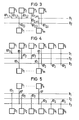
- Fig. 3 eine Mehrfachbusanordnung, bei der im prozessorabhängigen Busauswahlverfahren gearbeitet werden kann,
- Fig. 4 eine Mehrfachbusanordnung, bei dem die Prozessoren in Klassen verschiedenen Zugriffsprivilegs eingeteilt sind,
- Fig. 5 eine Mehrfachbusanordnung, bei der die Speicher in Klassen unterschiedlicher Zugriffszeiten eingeteilt sind,
- Fig. 6 eine Mehrfachbusanordnung für prozessorabhängiges Busauswahlverfahren, die redundant ist,
- Fig. 7 einen Aufbau eines Kopplers.
- 1 shows a multiple bus arrangement in which each processor and each memory is connected to each bus,
- 2 shows a multiple bus arrangement in which the memory-dependent bus selection method can be used,
- 3 shows a multiple bus arrangement in which the processor-dependent bus selection method can be used,
- 4 shows a multiple bus arrangement in which the processors are divided into classes with different access privileges,
- 5 shows a multiple bus arrangement in which the memories are divided into classes of different access times,
- 6 shows a multiple bus arrangement for processor-dependent bus selection method, which is redundant,
- Fig. 7 shows a structure of a coupler.
Fig. 1 zeigt eine Mehrfachbusanordnung für ein Mehrprozessorsystem, das z.B. aus der oben angegebenen Literaturstelle bekannt ist. Hier ist eine Mehrzahl von Bussen B1... Bi vorgesehen, an die Prozessoren P und Speicher S über Koppler K angeschlossen sind. Die Prozessoren P1...Pn sind jeweils über Prozessorverbindungsbusse PB1...PBn mit jeweils allen Bussen B1...Bi über Koppler KP verbindbar. Ebenso sind alle Speicher S1...Sm jeweils über Speicherverbindungsbusse SB1...SBm mit jeweils allen Bussen B1...Bi über Koppler KS verbindbar. Der Nachteil einer derartig ausgeführten Mehrfachbusanordnung besteht darin, daß eine Vielzahl von Kopplern KP bzw. KS erforderlich ist.1 shows a multiple bus arrangement for a multiprocessor system, for example from the literature cited above place is known. A plurality of buses B 1 ... B i are provided here, to which processors P and memory S are connected via couplers K. The processors P 1 ... P n can each be connected via processor connection buses PB 1 ... PB n to all buses B 1 ... B i via couplers KP. Likewise, all memories S 1 ... S m can each be connected via memory connection buses SB 1 ... SB m to all buses B 1 ... B i via couplers KS. The disadvantage of such a multiple bus arrangement is that a large number of couplers KP or KS is required.
Die Anzahl der Koppler in der Mehrfachbusanordnung wird dann verringert, wenn gemäß Fig. 2 das speicherabhängige Busauswahlverfahren gewählt wird. In Fig. 2 sind nur drei Busse B1, B2 und B3 dargestellt. Die Verbindung der Prozessoren P1 ... Pn mit den Bussen B1... B3 erfolgt entsprechend Fig. 1. Das heißt jeder Prozessor P1... Pn ist jeweils mit jedem Bus B1... B3 verbunden. Die Verbindung der Speicher S mit den Bussen B1... B3 ist jedoch unterschiedlich zur Figur 1. Hier ist jeder Speicher S jeweils nur mit einem Bus über einen Koppler KS verbindbar. Zum Beispiel ist der Speicher S1 nur mit dem Bus Bn über den Koppler KS1,1, der Speicher S2 nur mit dem Bus B2 über den Koppler KS2,2 und der Speicher S3 nur mit dem Bus B3 über den Koppler KS3,3 verbindbar. Es ist möglich, daß jeweils nur ein Speicher S mit einem Bus B verbindbar ist. Es ist jedoch auch möglich, wie in Fig. 2 dargestellt, daß mehr als ein Speicher S mit jeweils einem Bus verbunden ist. Da nunmehr nur jeweils ein Koppler KS pro Speicher S vorgesehen ist, und nicht mehr eine Vielzahl von Kopplern KS pro Speicher S wie in Fig. 1, kann die Anzahl der Koppler KS pro Mehrfachbusanordnung im speicherabhängigen Busauswahlverfahren erheblich verringert werden.The number of couplers in the multiple bus arrangement is reduced if the memory-dependent bus selection method is selected according to FIG. 2. In Fig. 2 only three buses B 1 , B 2 and B 3 are shown. The processors P 1 ... P n are connected to the buses B 1 ... B 3 in accordance with FIG. 1. That is, each processor P 1 ... P n is connected to each bus B 1 ... B 3 connected. However, the connection of the memories S to the buses B 1 ... B 3 is different from FIG. For example, the memory S 1 is only with the bus B n via the coupler KS 1,1 , the memory S 2 only with the bus B 2 via the coupler KS 2,2 and the memory S 3 only with the bus B 3 the coupler KS 3.3 can be connected . It is possible that only one memory S can be connected to one bus B at a time. However, as shown in FIG. 2, it is also possible for more than one memory S to be connected to one bus each. Since only one coupler KS per memory S is now provided, and no longer a plurality of couplers KS per memory S as in FIG. 1, the number of couplers KS per multiple bus arrangement can be considerably reduced in the memory-dependent bus selection method.
Beim speicherabhängigen Busauswahlverfahren hängt somit die Nummer des beim Zugriff angesprochenen Busses B von der Nummer des bei diesem Zugriff angesprochenen Speichers ab. Es gibt somit keine Speicherkonflikte. Wollen nämlich zwei Prozessoren gleichzeitig z.B. auf den Speicher S1 zugreifen, dann beanspruchen sie beide beim Zugriff den Bus B1. Dieser kann jeweils nur mit einem Zugriff befaßt sein und somit kann an den Speicher S1 jeweils nur eine Zugriffsanforderung gestellt werden. Dies ermöglicht Vereinfachungen der Hardware gegenüber Systemen mit zufallsbestimmter Busauswahl, die z.B. bei Fig. 1 möglich ist. Es sind nämlich wenige Anforderungsleitungen zwischen Bussen und Speichern nötig und Speicherarbiter können entfallen.With the memory-dependent bus selection process, it depends the number of the bus B addressed during the access from the number of the memory addressed during this access. There are therefore no storage conflicts. If, for example, two processors want to access memory S 1 at the same time, then they both occupy bus B 1 during access. This can each be concerned only with an access and thus only an access request can be provided respectively to the memory S1. This enables simplifications of the hardware compared to systems with random bus selection, which is possible, for example, in FIG. 1. This is because a few request lines between buses and memories are necessary and memory arbiters can be omitted.
In der Praxis ist es oft erwünscht, daß die Zuordnung zwischen Bussen und Speichern gleichmäßig ist, daß also jedem Bus gleichviele Speicher zugeordnet sind, wie in Fig. 2 gezeigt ist. Sind die Anzahl der Busse B und die An- .zahl der Speicher S Zweierpotenzen, dann läßt sich ein speicherabhängiges Busauswahlverfahren einfach dadurch realisieren, daß ein log2 (S) bit breites Binärwort als Speicheradresse verwendet wird und daraus irgendwelche bits, beispielsweise die höchstwertigen bits entnommen und als Busadresse verwendet werden.In practice, it is often desirable for the assignment between buses and memories to be uniform, that is, for each bus to have the same number of memories as shown in FIG. If the number of buses B and the number of memories S are powers of two, then a memory-dependent bus selection method can be implemented simply by using a log 2 (S) bit-wide binary word as the memory address and any bits therefrom, for example the most significant bits removed and used as bus address.
Eine Verringerung der Anzahl der Koppler kann aber auch dadurch erreicht werden, daß ein prozessorabhängiges Busauswahlverfahren gewählt wird, das in Fig. 3 dargestellt ist. Hier ist jeder Speicher S1 ... Sm jeweils mit jedem Bus über einen Koppler KS verbunden. Im Ausführungsbeispiel sind dies zwei Busse B1 und B2. Jeder Prozessor P ist dagegen jeweils nur mit einem Bus über einen Koppler KP verbunden. Somit ist pro Prozessor P nur noch jeweils ein Koppler notwendig und damit die Anzahl der Koppler pro Prozessor gegenüber der Ausführungsform der Fig. 1 erheblich geringer. So ist z.B. im Ausführungsbeispiel der Fig. 3 der Prozessor P1bzw.P2 nur mit dem Bus Bl,und der Prozessor P3 bzw. P4 nur jeweils mit dem Bus B 2 verbunden.However, a reduction in the number of couplers can also be achieved by choosing a processor-dependent bus selection method, which is shown in FIG. 3. Here, each memory S 1 ... S m is connected to each bus via a coupler KS. In the exemplary embodiment, these are two buses B 1 and B 2 . In contrast, each processor P is only connected to one bus via a coupler KP. Thus, only one coupler is required for each processor P, and the number of couplers per processor is considerably lower than in the embodiment of FIG. 1. For instance, the embodiment in Fig. 3, the processor P1bzw.P2 only connected to only the bus B l, and said processor P 3 and P 4 with the bus B2.
Bei einem prozessorabhängigen Busauswahlverfahren hängt die Wahl des Busses, der für den Zugriff verwendet wird, davon ab, welcher Prozessor den Zugriff ausführt. Wenn also z.B. der Prozessor P1 einen Zugriff ausführen will, muß er den Bus B benutzen, die Kopplung durch den Koppler KP1,1mit dem Bus B1 herbeiführen und kann dann jeden Speicher S1... Sm über die Koppler KS ansteuern.In a processor-dependent bus selection method, the choice of the bus used for the access depends on which processor carries out the access. If, therefore, will perform an access such as the processor P 1, he must use the bus B, to bring about the coupling by the coupler KP 1.1 to the bus B 1 and may then each store S 1 ... S m via the couplers KS head for.
Bei einem prozessorabhängigen Busauswahlverfahren lassen sich somit Anforderungsleitungen zwischen Prozessoren und Bussen und Koppler einsparen.With a processor-dependent bus selection process, request lines between processors and buses and couplers can be saved.
Der Wirkungsgrad einer Mehrfachbusanordnung kann dadurch gespeichert werden, daß gemäß Fig. 4 die Prozessoren in Klassen verschiedenen Zugriffsprivilegs eingeteilt werden. Dann wird jedem Bus eine von der Klasseneinteilung abhängige Anzahl von Prozessoren zugeteilt, so daß sich jeweils viele Prozessoren mit niedrigen Zugriffsprivilegien einen Bus teilen, jedoch jeweils nur wenige Prozessoren mit hohem Zugriffsprivileg an einem Bus angeschlossen sind. Im Beispiel der Fig. 4 hat der Prozessor P1 das höchste Zugriffsprivileg und ist nur mit einem Bus B1 verbunden. Zwei Prozessoren mit demnächstniedrigen Zugriffsprivileg, in Fig.4 mit PP,P3. bezeichnet, sind jeweils gemeinsam an einen zweiten Bus B2 angeschlossen. Drei Prozessoren P4,P5,P6 mit niedrigstem Zugriffsprivileg sind dagegen an den Bus B3 angeschlossen. Die Speicher S1 ... Sm sind dagegen jeweils mit allen Bussen B1... B3 über Koppler KS verbindbar.The efficiency of a multiple bus arrangement can be stored in that, according to FIG. 4, the processors are divided into classes with different access privileges. Then each bus is assigned a number of processors which is dependent on the class division, so that in each case many processors with low access privileges share a bus, but only a few processors with high access privilege are each connected to a bus. In the example of FIG. 4, the processor P 1 has the highest access privilege and is only connected to a bus B 1 . Two processors with the next lowest access privilege, in Fig. 4 with P P , P 3 . are connected to a second bus B 2 together . In contrast, three processors P 4 , P 5 , P 6 with the lowest access privilege are connected to the bus B 3 . The memories S 1 ... S m , on the other hand, can be connected to all buses B 1 ... B 3 via couplers KS.
Der Wirkungsgrad einer Mehrfachbusanordnung kann auch dadurch gesteigert werden, daß bei Speichern mit unterschiedlichen Zugriffszeiten eine Klasseneinteilung nach Zugriffszeiten erfolgt. Dann wird ein Bus jeweils wenigen schnellen oder vielen langsamen Speichern zugeordnet. In Fig. 5 hat z.B. der Speicher S1 die kleinste Zugriffszeit und ist nur mit einem Bus B1 über den Koppler KS1 verbindbar. Die zwei Speicher S2,S3haben gegenüber dem Speicher S1 eine höhere Zugriffszeit und sind gemeinsam an dem Bus B2 über die Koppler KS2 anschließbar. Die drei Speicher. S4,S5,S6 haben schließlich die höchste Zugriffszeit und sind gemeinsam am Bus B3 über die Koppler KS3 angeschlossen. Die Prozessoren P1 ... Pn sind dagegen jeweils mit allen Bussen B1 ... B3 über Kopp- ler KP verbindbar.The efficiency of a multiple bus arrangement can also be increased by classifying the memories with different access times according to access times. Then a bus is assigned to a few fast memories or many slow memories. 5, for example, the memory S 1 has the shortest access time and is only connectable to a bus B 1 via the coupler KS 1 . The two memories S 2 , S 3 have a higher access time than the memory S 1 and can be connected together to the bus B 2 via the coupler KS 2 . The three stores. S 4 , S 5 , S 6 finally have the highest access time and are connected together to bus B 3 via coupler KS 3 . The processors P 1 ... P n , on the other hand, can each be connected to all buses B 1 ... B 3 via couplers KP.
Die bisher erläuterten Mehrfachbusanordnungen der Fig. 2 bis 5 haben den Nachteil, daß bei Ausfall eines Kopplers oder eines Busses der zugeordnete Verbindungsweg unterbrochen ist und somit dieser Verbindungsweg für einen Zugriff nicht mehr benutzt werden kann. Da ein anderer Verbindungsweg nicht besteht, kann vom Prozessor auf den Speicher, zwischen denen der unterbrochene Verbindungsweg liegt, nicht mehr zugegriffen werden. Um dies zu vermeiden, kann die Mehrfachbusanordnung gemäß Fig. 6 derart ausgeführt sein, daß z.B. jeder Prozessor P mit jeweils zwei Bussen B1 und B2 überKoppler KP verbindbar ist. Fig. 6 zeigt dabei das prozessorabhängige Busauswahlverfahren, bei dem die Speicher S1 ... S3 jeweils mit allen Bussen B1 ... B3 verbunden sind. Soll bei einer derartigen Mehrfachbusanordnung z.B. der Prozessor P1 auf den Speicher S1 zugreifen und fällt z.B. der Koppler KP1 aus und damit der Verbindungsweg über den Bus B1, dann besteht noch der Verbindungsweg über den B2, den Koppler KP2 zum Speicher S1. Der Ausfall eines Kopplers oder eines Busses hindert somit nicht den Zugriff zu einem Speicher S.The previously explained multiple bus arrangements of FIGS. 2 to 5 have the disadvantage that if a coupler or a bus fails, the assigned connection path is interrupted and this connection path can therefore no longer be used for access. Since there is no other connection path, the processor can no longer access the memory between which the interrupted connection path lies. To avoid this, the multiple bus arrangement according to FIG. 6 can be designed such that, for example, each processor P can be connected to two buses B 1 and B 2 via couplers KP. 6 shows the processor-dependent bus selection method in which the memories S 1 ... S 3 are each connected to all buses B 1 ... B 3 . If, in such a multiple bus arrangement, processor P 1 , for example, is to access memory S 1 and, for example, coupler KP 1 fails and thus the connection path via bus B 1 , then there is still the connection path via B 2 , coupler KP 2 to the memory S 1 . The failure of a coupler or a bus does not prevent access to a memory S.
Entsprechend kann eine Mehrfachbusanordnung auch für ein speicherabhängiges Busauswahlverfahren aufgebaut sein. Dann ist jeder Prozessor P jeweils mit jedem Bus über einen Koppler verbindbar, dagegen jeder Speicher S jeweils mit zwei Bussen verbindbar. Fällt ein Koppler oder ein Bus aus, dann ist trotzdem über den anderen Koppler und über den anderen Bus ein Zugriff von einem Prozessor zu diesem Speicher möglich.Correspondingly, a multiple bus arrangement can also be constructed for a memory-dependent bus selection method. Then each processor P can be connected to each bus via a coupler, whereas each memory S can be connected to two buses. If a coupler or a bus fails, then access from a processor to this memory is still possible via the other coupler and the other bus.
Ein möglicher Aufbau der Koppler K ist in Fig. 7 dargestellt. Der Koppler K weist zwei Tristatetreiber TS1, TS2 auf, über die der Prozessorverbindungsbus PB, wie in Fig. 7, oder ein Speicherverbindungsbus mit dem Bus B verbindbar ist. Weiterhin ist eine Adressenerkennungslogik AEL vorgesehen, die erkennt, auf welchen Speicher über welchen Bus zugegriffen werden soll. Die entsprechende Adresse wird der Adressenerkennungslogik über den Prozessorverbindungsbus PB zugeführt. Gibt der Prozessor P eine dem Bus B zugeordnete Adresse ab, dann gibt die Adressenerkennungslogik AEL ein Signal REQ ab, das einem Arbiter ARB zugeleitet wird. Der Arbiter ARB überprüft, ob Zugriffswünsche von anderen Prozessoren vorliegen. Dazu ist er über Leitungen L1, L2, L3 mit den anderen Prozessoren zugeordneten Arbitern verbunden. Ergibt die überprüfung, daß der Prozessor P über den Bus B auf einen Speicher zugreifen darf, dann gibt der Arbiter ARB ein Signal ACK ab, das einen der Tristatetreiber TS ansteuert. Je nach dem, in welcher Richtung der Datenfluß gehen soll, wird entweder der Tristatetreiber TS1 oder der Tristatetreiber TS2 angesteuert.A possible construction of the coupler K is shown in FIG. 7. The coupler K has two tristate drivers TS 1 , TS 2 , via which the processor connection bus PB, as in FIG. 7, or a memory connection bus can be connected to the bus B. Furthermore, an address recognition logic AEL is provided, which recognizes which memory is to be accessed via which bus. The corresponding address is fed to the address recognition logic via the processor connection bus PB. If the processor P issues an address assigned to the bus B, the address recognition logic AEL issues a signal REQ which is fed to an arbiter ARB. The arbiter ARB checks whether there are requests for access from other processors. For this purpose, it is connected via lines L 1 , L 2 , L 3 to the arbiters assigned to the other processors. If the check shows that the processor P can access a memory via the bus B, the arbiter ARB emits a signal ACK which drives one of the tristate drivers TS. Depending on the direction in which the data flow should go, either the tristate driver TS 1 or the tristate driver TS 2 is controlled.
Die in Fig. 7 verwendeten Bausteine sind bekannte Bausteine. Zum Beispiel kann als Tristatetreiber ein Baustein 74241, als Arbiter ARB ein Intel-Arbitrationchip 8289 verwendet werden. Die Adressenerkennungslogik AEL kann als Komparator aufgebaut sein.The building blocks used in FIG. 7 are known building blocks. For example, a 74241 module can be used as the tri-state driver and an Intel arbitration chip 8289 can be used as the arbiter ARB. The address recognition logic AEL can be constructed as a comparator.
Die übrigen in der Mehrfachbusanordnung und dem Mehrprozessorsystem verwendeten Bausteine, also Prozessoren P, Speicher S oder Busse B, sind ebenfalls von bekanntem Aufbau.The other components used in the multiple bus arrangement and the multiple processor system, ie processors P, memory S or buses B, are likewise of a known design.
9 Patentansprüche, 7 Figuren9 claims, 7 figures
Claims (9)
Applications Claiming Priority (2)
| Application Number | Priority Date | Filing Date | Title |
|---|---|---|---|
| DE19833338341 DE3338341A1 (en) | 1983-10-21 | 1983-10-21 | MULTIPLE BUS ARRANGEMENT FOR CONNECTING PROCESSORS AND STORAGE IN A MULTIPROCESSOR SYSTEM |
| DE3338341 | 1983-10-21 |
Publications (2)
| Publication Number | Publication Date |
|---|---|
| EP0141332A2 true EP0141332A2 (en) | 1985-05-15 |
| EP0141332A3 EP0141332A3 (en) | 1986-09-10 |
Family
ID=6212458
Family Applications (1)
| Application Number | Title | Priority Date | Filing Date |
|---|---|---|---|
| EP84112409A Withdrawn EP0141332A3 (en) | 1983-10-21 | 1984-10-15 | Arrangement with a plurality of buses for the connection of processors and memories in a multiprocessor system |
Country Status (2)
| Country | Link |
|---|---|
| EP (1) | EP0141332A3 (en) |
| DE (1) | DE3338341A1 (en) |
Cited By (7)
| Publication number | Priority date | Publication date | Assignee | Title |
|---|---|---|---|---|
| EP0458516A2 (en) * | 1990-05-25 | 1991-11-27 | AT&T Corp. | Memory access bus arrangement |
| EP0494056A2 (en) * | 1990-12-31 | 1992-07-08 | International Business Machines Corporation | Dynamically partitionable and allocable bus structure |
| EP0335968B1 (en) * | 1987-10-16 | 1993-08-04 | Digital Equipment Corporation | Computer interconnect coupler employing crossbar switching |
| WO1996030842A1 (en) * | 1995-03-27 | 1996-10-03 | International Business Machines Corporation | Bus structure for a multiprocessor system |
| GB2332344A (en) * | 1997-12-09 | 1999-06-16 | Sony Uk Ltd | Set top box integrated circuit |
| WO2000043894A2 (en) * | 1999-01-21 | 2000-07-27 | Analog Devices, Inc. | Method and apparatus for communicating between multiple functional units in a computer environment |
| WO2001009741A2 (en) * | 1999-07-30 | 2001-02-08 | Siemens Aktiengesellschaft | Multiprocessor system for executing memory accesses to a common memory and a corresponding method |
Families Citing this family (3)
| Publication number | Priority date | Publication date | Assignee | Title |
|---|---|---|---|---|
| FI84114C (en) * | 1988-02-17 | 1991-10-10 | Valtion Teknillinen | Switching System |
| DE4143584C2 (en) * | 1990-06-04 | 2002-10-10 | Hitachi Ltd | Bus system for information processing appts. |
| DE19841183C2 (en) * | 1998-09-09 | 2000-08-10 | Daimler Chrysler Ag | Device for coupling redundant electronic circuits via redundant buses without error propagation |
Citations (1)
| Publication number | Priority date | Publication date | Assignee | Title |
|---|---|---|---|---|
| US3787818A (en) * | 1971-06-24 | 1974-01-22 | Plessey Handel Investment Ag | Mult-processor data processing system |
-
1983
- 1983-10-21 DE DE19833338341 patent/DE3338341A1/en not_active Withdrawn
-
1984
- 1984-10-15 EP EP84112409A patent/EP0141332A3/en not_active Withdrawn
Patent Citations (1)
| Publication number | Priority date | Publication date | Assignee | Title |
|---|---|---|---|---|
| US3787818A (en) * | 1971-06-24 | 1974-01-22 | Plessey Handel Investment Ag | Mult-processor data processing system |
Non-Patent Citations (2)
| Title |
|---|
| ELEKTRONIK, Band 32, Nr. 20, 7. Oktober 1983, Seiten 75-79, M}nchen, DE; G. ANGELE et al.: "Octobus: ein universelles Mikrorechnerkonzept" * |
| SIMULATION, Band 31, Nr. 5, November 1978, Seiten 145-153, Simulation Councils Inc., La Jolla, California, US; L.D. WITTIE: "MICRONET: a reconfigurable microcomputer network for distributed systems research" * |
Cited By (14)
| Publication number | Priority date | Publication date | Assignee | Title |
|---|---|---|---|---|
| EP0335968B1 (en) * | 1987-10-16 | 1993-08-04 | Digital Equipment Corporation | Computer interconnect coupler employing crossbar switching |
| EP0458516A2 (en) * | 1990-05-25 | 1991-11-27 | AT&T Corp. | Memory access bus arrangement |
| EP0458516A3 (en) * | 1990-05-25 | 1992-04-08 | American Telephone And Telegraph Company | Memory access bus arrangement |
| EP0494056A2 (en) * | 1990-12-31 | 1992-07-08 | International Business Machines Corporation | Dynamically partitionable and allocable bus structure |
| EP0494056A3 (en) * | 1990-12-31 | 1994-08-10 | Ibm | Dynamically partitionable and allocable bus structure |
| WO1996030842A1 (en) * | 1995-03-27 | 1996-10-03 | International Business Machines Corporation | Bus structure for a multiprocessor system |
| GB2332344A (en) * | 1997-12-09 | 1999-06-16 | Sony Uk Ltd | Set top box integrated circuit |
| EP0923232A3 (en) * | 1997-12-09 | 2002-02-13 | Sony United Kingdom Limited | Set Top Box integrated circuit |
| WO2000043894A2 (en) * | 1999-01-21 | 2000-07-27 | Analog Devices, Inc. | Method and apparatus for communicating between multiple functional units in a computer environment |
| WO2000043894A3 (en) * | 1999-01-21 | 2001-02-08 | Analog Devices Inc | Method and apparatus for communicating between multiple functional units in a computer environment |
| US6618777B1 (en) | 1999-01-21 | 2003-09-09 | Analog Devices, Inc. | Method and apparatus for communicating between multiple functional units in a computer environment |
| CN1315069C (en) * | 1999-01-21 | 2007-05-09 | 模拟装置公司 | Method and apparatus for communicating between multiple functional units in computer environment |
| WO2001009741A2 (en) * | 1999-07-30 | 2001-02-08 | Siemens Aktiengesellschaft | Multiprocessor system for executing memory accesses to a common memory and a corresponding method |
| WO2001009741A3 (en) * | 1999-07-30 | 2001-08-30 | Siemens Ag | Multiprocessor system for executing memory accesses to a common memory and a corresponding method |
Also Published As
| Publication number | Publication date |
|---|---|
| DE3338341A1 (en) | 1985-05-09 |
| EP0141332A3 (en) | 1986-09-10 |
Similar Documents
| Publication | Publication Date | Title |
|---|---|---|
| DE3938018C3 (en) | Information processing system and method for determining its configuration | |
| DE3909948C2 (en) | ||
| DE69915243T2 (en) | Disk array control device | |
| DE2829550C2 (en) | ||
| DE69736872T2 (en) | Data processing system | |
| DE3146356A1 (en) | DATA PROCESSING SYSTEM | |
| DE2313724A1 (en) | ELECTRONIC DATA PROCESSING SYSTEM | |
| CH657714A5 (en) | MULTI-PROCESSOR SYSTEM. | |
| DE3049774C2 (en) | ||
| DE2523372B2 (en) | Input-output port controller | |
| DE4017902A1 (en) | ADDITIONAL CARD WITH AUTOMATIC ADJUSTMENT TO THE SLOT POSITION | |
| DE4135830C2 (en) | Parallel interface | |
| DE3535436C2 (en) | ||
| EP0141332A2 (en) | Arrangement with a plurality of buses for the connection of processors and memories in a multiprocessor system | |
| EP0062141B1 (en) | Circuit arrangement for entering control commands into a microcomputer system | |
| WO1996016366A1 (en) | Arrangement with master and slave units | |
| DE3142504A1 (en) | MULTIPLE DISK STORAGE TRANSMISSION SYSTEM | |
| DE3009530A1 (en) | DATA PROCESSING SYSTEM | |
| DE2142374C2 (en) | Circuit arrangement for the selection and, if necessary, modification of data characters | |
| WO1994012936A1 (en) | Arrangement for transmitting data over a bus | |
| DE3247083A1 (en) | MULTI-PROCESSOR SYSTEM | |
| DE2217609A1 (en) | Access unit for data processing systems | |
| DE3325791C2 (en) | Circuit arrangement for peripheral units cooperating with a central control device | |
| DE3917715A1 (en) | COMPUTER SYSTEM | |
| DE3631086C2 (en) | Circuit arrangement for error processing in microprocessor systems |
Legal Events
| Date | Code | Title | Description |
|---|---|---|---|
| PUAI | Public reference made under article 153(3) epc to a published international application that has entered the european phase |
Free format text: ORIGINAL CODE: 0009012 |
|
| AK | Designated contracting states |
Designated state(s): AT CH DE FR GB IT LI |
|
| RTI1 | Title (correction) | ||
| 17P | Request for examination filed |
Effective date: 19850827 |
|
| PUAL | Search report despatched |
Free format text: ORIGINAL CODE: 0009013 |
|
| AK | Designated contracting states |
Kind code of ref document: A3 Designated state(s): AT CH DE FR GB IT LI |
|
| 17Q | First examination report despatched |
Effective date: 19880719 |
|
| STAA | Information on the status of an ep patent application or granted ep patent |
Free format text: STATUS: THE APPLICATION IS DEEMED TO BE WITHDRAWN |
|
| 18D | Application deemed to be withdrawn |
Effective date: 19890503 |
|
| RIN1 | Information on inventor provided before grant (corrected) |
Inventor name: JEFFRE, THOMAS, DIPL.-INFORM. |