EP0145530A2 - Arrangement for providing data signals for a data display system - Google Patents
Arrangement for providing data signals for a data display system Download PDFInfo
- Publication number
- EP0145530A2 EP0145530A2 EP84402086A EP84402086A EP0145530A2 EP 0145530 A2 EP0145530 A2 EP 0145530A2 EP 84402086 A EP84402086 A EP 84402086A EP 84402086 A EP84402086 A EP 84402086A EP 0145530 A2 EP0145530 A2 EP 0145530A2
- Authority
- EP
- European Patent Office
- Prior art keywords
- signals
- bit
- microprocessor
- map memory
- buffer
- Prior art date
- Legal status (The legal status is an assumption and is not a legal conclusion. Google has not performed a legal analysis and makes no representation as to the accuracy of the status listed.)
- Withdrawn
Links
Images
Classifications
-
- G—PHYSICS
- G06—COMPUTING; CALCULATING OR COUNTING
- G06F—ELECTRIC DIGITAL DATA PROCESSING
- G06F3/00—Input arrangements for transferring data to be processed into a form capable of being handled by the computer; Output arrangements for transferring data from processing unit to output unit, e.g. interface arrangements
- G06F3/14—Digital output to display device ; Cooperation and interconnection of the display device with other functional units
-
- G—PHYSICS
- G09—EDUCATION; CRYPTOGRAPHY; DISPLAY; ADVERTISING; SEALS
- G09G—ARRANGEMENTS OR CIRCUITS FOR CONTROL OF INDICATING DEVICES USING STATIC MEANS TO PRESENT VARIABLE INFORMATION
- G09G5/00—Control arrangements or circuits for visual indicators common to cathode-ray tube indicators and other visual indicators
- G09G5/36—Control arrangements or circuits for visual indicators common to cathode-ray tube indicators and other visual indicators characterised by the display of a graphic pattern, e.g. using an all-points-addressable [APA] memory
- G09G5/39—Control of the bit-mapped memory
- G09G5/393—Arrangements for updating the contents of the bit-mapped memory
Definitions
- the CRT beam In order to show on a cathode ray tube (CRT) screen some image, whether it be text or graphics, the CRT beam must be turned on (brightened in the case of the image being bright and the background dull) at the correct time to produce a dot, or a series of dots to make a bar, and the like.
- the display system have a data storage means which transmits data signals, representing the image to be displayed, in synchronism with clock signals from a clock signal generator.
- the clock generator is usually located in the CRT circuitry. In synchronism with the clock signals the CRT beam is turned on (or not turned on) as the beam gets to the correct data location. It should be understood that in the case of the intelligence being in a dark mode, against a bright background, then the beam would be turned off. All of the foregoing is well understood in the prior art.
- bit map memory there is a memory for each pixel location on the CRT screen.
- image can be written into the bit map memory and from that one memory (as it is scanned) both graphics and text data signals can be transmitted to the CRT screen to be shown.
- bit map memory was not used for text but the text was encoded from a character generator and continually transmitted to the CRT. While the prior art system was fast, it required two separate memory systems. The present system permits both text and graphics to use the same memory while operating with the speed of the separate memories of the prior art.
- the present invention employs a five-fold improvement in transmitting data signals to the data display device as will be explained below.
- the system in accordance with the invention employs a microprocessor as a dedicated slave device to a main data processing system.
- the microprocessor responds to groups of coded signals from the main data processing system.
- the present system provides a raster of bit signals from a ROM means, which bit signals graphically define the text character assigned to the coded set of signals being received.
- a raster of bit signals from a ROM means, which bit signals graphically define the text character assigned to the coded set of signals being received.
- that group of signals causes, in a preferred embodiment, the generation of a raster of 8 by 10 bits from the ROM in the microprocessor.
- ten bytes of data are stored in ROM memory means for each possible text character to be shown.
- the raster of bit signals are block transferred from the ROM of the microprocessor to buffer. Thereafter the bit signal raster, which has been properly arranged, is transferred in parallel during sync signal blank periods.
- a graphic display controller device provides addresses to the bit map memory so that a block transfer is written into the bit map memory at a particular starting address.
- the microprocessor is programmed to determine whether a block transfer requires one or two cycles and accordingly characters are transferred from the buffer in either one step or two steps.
- the bit signals in the buffer are located to match where, within a word location, in the bit map memory they are to be ultimately located.
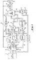
- Figure 1 there is shown a main computer 11 which is connected by channel 13 to a microprocessor 15.
- the main computer 11 is the heart of a computing system and is connected to many terminals and peripherals which are not shown in Figure 1.
- the channels shown throughout Figure 1 comprise a plurality of parallel wires and the signals transmitted over these channels include address signals, instruction signals, and data to be displayed signals.
- the microprocessor in a preferred embodiment is an 8085 manufactured by Intel Corporation.
- the microprocessor 15 includes at least a central processing unit, ROM memory means, RAM memory means and logic circuitry to generate instruction information signals.
- FIG. 1 there is a buffer 23 connected by channel 21 to RAM 18 of the microprocessor 15.
- the present system operates with a 16-bit word that is broken up into two 8-bit bytes.
- the ROM 16 there is stored a plurality of 8 by 10 bit rasters, each of which configures a character to be displayed.
- the letter "D" would be graphically represented by bit signals stored in an appropriate location in the ROM.
- bit signals when the raster of bit signals is transmitted from the ROM, it is transmitted through the central processing unit of the microprocessor back into the RAM 18, and in the course of that action the bit signals are revolved so that when they are transmitted from the RAM 18 along channel 21 to buffer 23, they end up in the proper locations for transmission to the bit map memory 33.
- the arranging of the bits etc. will be more clearly understood from the discussion of Figures 2 through 5.
- the buffer 23 is formed to store 16 bits in a row and to store 10 rows.
- One character at a time is transferred from the RAM 18 to the buffer 23.
- the bit signals stored in the buffer 23, representing the character are transferred in parallel, 16 bits at a time, through the multiplexer (hereinafter MUX) 27 along channel 37 and into the bit map memory 33.
- MUX multiplexer
- the bit signals from the buffer 23 are located in the bit map memory in accordance with address signals present on channel 39.
- the graphic display controller 19 is connected to the microprocessor 15 through the channel 17.
- the graphic display controller (hereinafter referred to as the GDC) is a MICRO PD 7220 manufactured by NEC Corporation.
- the GDC 19 has memory means to store address and instruction information from the microprocessor and also includes two registers which can be incremented or decremented to accomplish the changing of an address.
- the GDC 19 also includes a write signal generator which provides clock signals as well as horizontal and vertical sync signals. The sync signals are transmitted on connection 57 to the CRT 51, to the shift register 53 and to the microprocessor 15. Write clock signals are transmitted to the buffer 23 and to destination counter 41 over connection 31.
- the horizontal and vertical sync signals operate within the GDC 19 to accomplish certain operations therein. For every horizontal blank period there are seven write cycles generated and for every vertical blank period there are 594 write cycles generated. Other rates could be used.
- the destination counter 41 is included in the layout in Figure 1 because it is part of an overall system. However, it is not employed with the invention described in this description. The operation of the destination counter 41 is described in my co-pending application entitled, "Split Screen Smooth Scrolling Arrangement", serial number
- the GDC 19 accepts address information and instruction information from the microprocessor 15 and holds that information to effect address signals on channel 39 so that characters being transferred from the buffer 23 are properly located in the bit map memory 33.
- the GDC 19 transmits its address information along channel 25, along channel 35, through MUX 29, through decoder 45, onto the channel 39.
- the MUX 29 has a second input on channel 43, from the destination counter 41, but as was mentioned above, that circuitry plays no role in the operation of the present invention. Insofar as the present invention is concerned, it can be assumed that the address information from the GDC 19 always goes through the MUX 29, i.e., that the MUX 29 is not even present.
- the decoder 45 takes the address information and decodes it into the proper signals to operate with the bit map memory 33. In a preferred embodiment the decoder 45 is a 74LS253, manufactured by Texas Instruments Corporation.
- channel 91 and latch 93 are also circuitry elements which are used in connection with a split-screen smooth scrolling circuit described in the aforementioned copending application, i.e., channel 91, latch 93, and channel 97 play no role in the operation of the present invention.
- bit signals or pixel signals being transmitted from the bit map memory 33 are transmitted along channel 56 to shift register 53.
- the signals are advanced from shift register 53 in response to horizontal sync signals on connection 57.
- the signals on channel 58 are transmitted in synchronism with the horizontal sync signal, they are present in synchronism with the beam of the CRT, which is what is required to provide the display.
- FIG. 1 there is shown a MUX 31 which has two inputs, namely channels 49 and 47.
- bit signals When bit signals are being transmitted from the buffer 23, through MUX 27 and along channel 37, certain of those signals must be masked so that only the proper connections in the bit wire bit map memory are energized.
- the microprocessor 15 through its CPU keeps an account of what signals, or what signals from the buffer device 23, require masking and hence a set of masked signals are transmitted on channel 49 to MUX 31.
- the signals on channel 49 in turn energize or do not energize certain write enable signals on channel 40 and the system in effect electronically masks certain signals on channel 37.
- the other input to the MUX 31 is channel 47 which comes from the GDC.
- the GDC 19 has the ability to transmit graphic display signals along channel 25 and the channel 35, through the MUX 27, and along channel 37. While that capability is present in the system shown in Figure 1, it does not become part of the present invention.
- the present invention is directed to accelerating the signals representing text characters from the main computer 11 to the C R T 51.
- the five-fold feature of the present invention which acts together to accelerate the signals representing the characters includes the concept of using the microprocessor 15 as a dedicated slave. In accordance with this dedication, a group of 8-bit ASCII coded signals sent on channel 13 is immediately transformed into an 8 by 10 bit raster read out of ROM 16. That 8 by 10 bit raster of bit signals is immediately transformed into a 16 by 10 bit raster in the RAM 18 and then transferred to buffer 23.
- the third feature lies in the capability of buffer 23 to transmit the bit signals in parallel and hence the proper locating of the bit signals in the bit map memory is speeded up because of the parallel transmission.
- the parallel transmissions are accomplished during blank periods and this fourth feature also adds to the overall speeding up of the operation since the transmissions are taking place during time periods which otherwise might not be used.
- the fifth feature of the present invention is the use of the GDC 19 which provides the address information and monitors the address information so that the buffer sends its signals into the bit map memory at the proper addresses. As was mentioned earlier, the GDC has two registers.
- the "present" address register there is initially located the starting address to which the information in the buffer 23 will be sent and located.
- the starting address register is incremented.
- the region ending value register will initially be loaded with the value of ten in the preferred embodiment because the buffer 23 will have ten words stored therein and the operation is such that the buffer will be completely emptied before it is reloaded. Accordingly, in response to the write signals, the region ending value register will be decremented.
- the region ending value register has a value of zero, the microprocessor is informed by the GDC that buffer 23 can be reloaded. The feature of having such traffic control outside of the microprocessor adds to the overall speed of the operation.
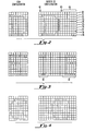
- FIGs 2, 3 and 4 there is depicted on the left-hand side the arrangement of the bit signals in the ROM.
- the letter “D” in Figure 2 is shown in the ROM in an 8 by 10 configuration and it will be noted that the top row of the 8 by 10 raster is left blank. The reason that the top row is left blank is so that when the letters are joined together on the screen, there will be space between the rows of letters.
- the letter "E” is shown in the ROM on the left-hand side in an 8 by 10 configuration
- Figure 4 the letter “C” is shown in the ROM in an 8 by 10 configuration.
- the microprocessor 15 is programmed to accommodate a number of formats. The microprocessor 15 knows that upon the first transfer of a raster of bit signals from the buffer 23, the letter will be configured in the first ten bits, and hence the control signals on channel 49 to the MUX 31 dictate that the mask effected on channel 40 will mask out the last six bit positions depicted as columns 65 in Figure 2.
- Figure 5 there is shown the organization of four addresses in the bit map memory 33. At each of the addresses 0, 1, 2, and 3 (designated as addresses in Figure 5) the bit map memory can store 16 bits or one word. The 16 bit locations are designated as 0 through 15.
- the first row represents the memory elements for the pixel locations on the CRT. It can be seen in Figure 5 that all of these first row locations are blank. It will be recalled that the top row of the raster in the ROM is blank to provide a space between rows of words on the display, hence this first row is blank.
- the second row in Figure 5 shows the bit signals which would be transferred to transfer the second row of each of the letter "D,” “E” and “C” as depicted in Figures 2, 3 and 4.
- the bit signals are transferred from the buffer into the bit map memory as shown in Figure 5.
- the buffer is shown storing the second row of bit information (depicted in Figure 2).
- the microprocessor 15 When the second row of bit information is being transferred from the buffer 23, through the MUX 27, along channel 37, the microprocessor 15 provides the masking information to the MUX 31 so that the last six pixel locations are masked or blanked and this is indicated in Figure 5 at location 67 by the x's. Accordingly, loaded into the second row of the bit map memory at the positions 0 through 9, we see that the bit signals are the same as the bit signals in the first ten positions of the location 67.
- the starting address in the present address register in the GDC started out with the address 0, and the blank information shown in the first row was transmitted from the buffer into the bit map memory. At that time the region length value register in the GDC 19 was decremented.
- the present address register in the GDC is incremented by 50, and hence the second row in the bit map memory and its positions 0 through 9 are loaded as shown in position 69.
- the length register will be decremented and the operation continues until each of the rows 70 through 79 shown in Figure 2 has been transferred from the buffer 23, through the MUX 27, along the channel 37 to the bit map memory. Since each of these transfers requires that the last six positions be masked, the mask information on 49 remains constant until there has been a transfer of a complete character from the buffer 23 to the bit map memory 33.
- the GDC advises the microprocessor that a new character can be transferred from the ROM 16 througg the RAM 18 to buffer 23.
- seven words from the buffer 23 can be transferred to the bit map memory during a horizontal blank period. Accordingly at the end of such a horizontal blank period the GDC will have its present address register reading 400 or the eighth line and the length ending address register will be set at 3.
- the remaining three rows namely rows 77 through 79 in Figure 2, will be transferred from the buffer 23 to the bit map memory.
- the microprocessor 15 will load the letter "E" from the ROM 16 through the RAM 18 into the buffer 23 and the process will repeat itself.
- bit map memory In location 80 of Figure 5 it can be noted that the 0 through 9 bit positions would be masked (indicated by x's)and only the information in bit positions 10 through 15 would be transferred to the bit map memory.
- the system would repeat the operation, always masking the first ten positions until the bit map memory is loaded with the information shown in section 81 of Figure 3. At this time the registers of the GDC would indicate to the microprocessor that section 81 had been loaded.
- the microprocessor 15 is programmed to know that during the second operation there must be second unloading of the buffer 23 and at that time positions 4 through 15 must be masked as shown by section 83 in Figure 5.
- section 83 in Figure 5
- the first three bits plus the blank right-hand column (shown in section 85 of Figure 3) are being transferred to the bit map memory and that the positions 4 through 15 are masked out.
- the GDC in the meantime has changed the address from 0 to 1 and hence the three bits plus the blank column are located in positions 0, 1, 2 and 3 of address 1 in the bit map memory.
- the registers in GDC 19 indicate to the microprocessor that the loading of section 85 has .been completed, the microprocessor will commence to load the letter "C" from the ROM 16 through RAM 18 into the buffer 23 as shown in the buffer configuration of Figure 4.
- bit signals are located in the buffer within a word configuration in the same way that they will be loaded into the bit map memory within a word configuration, and this of course saves time in the ultimate transferring of the information into the bit map memory.
- the use of the microprocessor 15 as a dedicated slave for the purpose of encoding a few signals into a large number of signals increases the speed with which the information is transferred from the main computer to the CRT.
- the description of Figures 2-5 in conjunction with the understanding of Figure 1 makes it clear that the transfer of the information from the buffer 23 in parallel, during blank times in response to the write clock signals, rapidly increases the transfer of the information from the main computer to the CRT 51.
- the use of the GDC to provide the starting addresses and to keep track of which addresses are in effect as well as when the character has been transferred, contributes to the speed of the overall operation.
Abstract
Description
- In order to show on a cathode ray tube (CRT) screen some image, whether it be text or graphics, the CRT beam must be turned on (brightened in the case of the image being bright and the background dull) at the correct time to produce a dot, or a series of dots to make a bar, and the like. The foregoing necessitates that the display system have a data storage means which transmits data signals, representing the image to be displayed, in synchronism with clock signals from a clock signal generator. In the prior art, the clock generator is usually located in the CRT circuitry. In synchronism with the clock signals the CRT beam is turned on (or not turned on) as the beam gets to the correct data location. It should be understood that in the case of the intelligence being in a dark mode, against a bright background, then the beam would be turned off. All of the foregoing is well understood in the prior art.
- Further in the major part of the prior art, if a system is going to display both graphics and text, two different memory and control systems have been employed. It has been only when the information is finally transmitted to the CRT device that the graphics and text signals have been meshed, or multiplexed.
- The introduction of the bit map memory, to the display art, has made the task somewhat easier because in a bit map memory, there is a memory for each pixel location on the CRT screen. Hence, whatever image is to be seen (either text, or graphics, or a combination of both) can be written into the bit map memory and from that one memory (as it is scanned) both graphics and text data signals can be transmitted to the CRT screen to be shown.
- The major problem that occurs in the prior art is that the bit map memory was not used for text but the text was encoded from a character generator and continually transmitted to the CRT. While the prior art system was fast, it required two separate memory systems. The present system permits both text and graphics to use the same memory while operating with the speed of the separate memories of the prior art. The present invention employs a five-fold improvement in transmitting data signals to the data display device as will be explained below.
- The system in accordance with the invention employs a microprocessor as a dedicated slave device to a main data processing system. The microprocessor responds to groups of coded signals from the main data processing system. In response to each group of coded signals, the present system provides a raster of bit signals from a ROM means, which bit signals graphically define the text character assigned to the coded set of signals being received. In other words, if eight bits of ASCII coded signals are transmitted from the main data processing device, that group of signals causes, in a preferred embodiment, the generation of a raster of 8 by 10 bits from the ROM in the microprocessor. In the microprocessor, ten bytes of data are stored in ROM memory means for each possible text character to be shown. The raster of bit signals are block transferred from the ROM of the microprocessor to buffer. Thereafter the bit signal raster, which has been properly arranged, is transferred in parallel during sync signal blank periods. To effect this block transfer, a graphic display controller device provides addresses to the bit map memory so that a block transfer is written into the bit map memory at a particular starting address.
- The microprocessor is programmed to determine whether a block transfer requires one or two cycles and accordingly characters are transferred from the buffer in either one step or two steps. The bit signals in the buffer are located to match where, within a word location, in the bit map memory they are to be ultimately located. The dedication of the microprocessor to providing encoded signals, the speed of the parallel transfer, the fact that the transfer is made during the horizontal and vertical blank periods, utilization of the graphic display controller to provide the addresses, and the prearrangement of the bits in the buffer enable the data transfer to be more rapidly accomplished than in the prior art.
- The objects and features of the present invention will be better understood after studying the description below taken in conjunction with the drawings wherein:
- Figure 1 is a block schematic diagram of the present system;
- Figure 2 depicts the letter "D" as it appears in the ROM and as it later appears in the buffer;
- Figure 3 depicts the letter "E" as it appears in the ROM and as it later appears in the buffer;
- Figure 4 depicts the letter "C" as it appears in the ROM and as it later appears in the buffer; and
- Figure 5 depicts the transfer of bit signals from the buffer to the bit map memory.
- In Figure 1 there is shown a main computer 11 which is connected by
channel 13 to amicroprocessor 15. It should be understood that the main computer 11 is the heart of a computing system and is connected to many terminals and peripherals which are not shown in Figure 1. It should also be understood that the channels shown throughout Figure 1 comprise a plurality of parallel wires and the signals transmitted over these channels include address signals, instruction signals, and data to be displayed signals. The microprocessor in a preferred embodiment is an 8085 manufactured by Intel Corporation. It should be understood that themicroprocessor 15 includes at least a central processing unit, ROM memory means, RAM memory means and logic circuitry to generate instruction information signals. - As can be gleaned from Figure 1 there is a
buffer 23 connected bychannel 21 toRAM 18 of themicroprocessor 15. The present system operates with a 16-bit word that is broken up into two 8-bit bytes. In theROM 16 there is stored a plurality of 8 by 10 bit rasters, each of which configures a character to be displayed. In other words, as will become clearer hereinafter, the letter "D" would be graphically represented by bit signals stored in an appropriate location in the ROM. Also as will become clearer hereinafter, when the raster of bit signals is transmitted from the ROM, it is transmitted through the central processing unit of the microprocessor back into theRAM 18, and in the course of that action the bit signals are revolved so that when they are transmitted from theRAM 18 alongchannel 21 tobuffer 23, they end up in the proper locations for transmission to thebit map memory 33. The arranging of the bits etc. will be more clearly understood from the discussion of Figures 2 through 5. - The
buffer 23 is formed to store 16 bits in a row and to store 10 rows. One character at a time is transferred from theRAM 18 to thebuffer 23. The bit signals stored in thebuffer 23, representing the character, are transferred in parallel, 16 bits at a time, through the multiplexer (hereinafter MUX) 27 alongchannel 37 and into thebit map memory 33. As will become clearer in the discussion of Figures 2 through 5, when the bit signals are transmitted into the bit map memory, six of those bits are masked out onchannel 40. The bit signals from thebuffer 23 are located in the bit map memory in accordance with address signals present onchannel 39. - As can also be gleaned from an examination of Figure 1, there is a
graphic display controller 19 connected to themicroprocessor 15 through thechannel 17. In a preferred embodiment the graphic display controller (hereinafter referred to as the GDC) is a MICRO PD 7220 manufactured by NEC Corporation. The GDC 19 has memory means to store address and instruction information from the microprocessor and also includes two registers which can be incremented or decremented to accomplish the changing of an address. The GDC 19 also includes a write signal generator which provides clock signals as well as horizontal and vertical sync signals. The sync signals are transmitted on connection 57 to theCRT 51, to theshift register 53 and to themicroprocessor 15. Write clock signals are transmitted to thebuffer 23 and todestination counter 41 overconnection 31. In addition, the horizontal and vertical sync signals operate within the GDC 19 to accomplish certain operations therein. For every horizontal blank period there are seven write cycles generated and for every vertical blank period there are 594 write cycles generated. Other rates could be used. - The
destination counter 41 is included in the layout in Figure 1 because it is part of an overall system. However, it is not employed with the invention described in this description. The operation of thedestination counter 41 is described in my co-pending application entitled, "Split Screen Smooth Scrolling Arrangement", serial number - and which is assigned to the assignee of this application. The
GDC 19 accepts address information and instruction information from themicroprocessor 15 and holds that information to effect address signals onchannel 39 so that characters being transferred from thebuffer 23 are properly located in thebit map memory 33. - As can be seen in Figure 1, the GDC 19 transmits its address information along
channel 25, alongchannel 35, through MUX 29, throughdecoder 45, onto thechannel 39. The MUX 29 has a second input onchannel 43, from thedestination counter 41, but as was mentioned above, that circuitry plays no role in the operation of the present invention. Insofar as the present invention is concerned, it can be assumed that the address information from the GDC 19 always goes through theMUX 29, i.e., that theMUX 29 is not even present. Thedecoder 45 takes the address information and decodes it into the proper signals to operate with thebit map memory 33. In a preferred embodiment thedecoder 45 is a 74LS253, manufactured by Texas Instruments Corporation. Those signals are held in the latch so that they are present when the bit signals onchannel 37 arrive at thebit map memory 33. It should also be noted thatchannel 91 and latch 93 are also circuitry elements which are used in connection with a split-screen smooth scrolling circuit described in the aforementioned copending application, i.e.,channel 91,latch 93, andchannel 97 play no role in the operation of the present invention. - When the characters have been stored in the
bit map memory 33, they are read therefrom in response to address signals onchannel 39. The bit signals or pixel signals being transmitted from thebit map memory 33 are transmitted alongchannel 56 to shiftregister 53. The signals are advanced fromshift register 53 in response to horizontal sync signals on connection 57. When the signals are advanced fromshift register 53 they pass alongchannel 58 to theCRT 51. Since the signals onchannel 58 are transmitted in synchronism with the horizontal sync signal, they are present in synchronism with the beam of the CRT, which is what is required to provide the display. - In Figure 1 there is shown a
MUX 31 which has two inputs, namelychannels buffer 23, throughMUX 27 and alongchannel 37, certain of those signals must be masked so that only the proper connections in the bit wire bit map memory are energized. Themicroprocessor 15 through its CPU keeps an account of what signals, or what signals from thebuffer device 23, require masking and hence a set of masked signals are transmitted onchannel 49 toMUX 31. The signals onchannel 49 in turn energize or do not energize certain write enable signals onchannel 40 and the system in effect electronically masks certain signals onchannel 37. The other input to theMUX 31 ischannel 47 which comes from the GDC. TheGDC 19 has the ability to transmit graphic display signals alongchannel 25 and thechannel 35, through theMUX 27, and alongchannel 37. While that capability is present in the system shown in Figure 1, it does not become part of the present invention. The present invention is directed to accelerating the signals representing text characters from the main computer 11 to the CRT 51. The five-fold feature of the present invention which acts together to accelerate the signals representing the characters includes the concept of using themicroprocessor 15 as a dedicated slave. In accordance with this dedication, a group of 8-bit ASCII coded signals sent onchannel 13 is immediately transformed into an 8 by 10 bit raster read out ofROM 16. That 8 by 10 bit raster of bit signals is immediately transformed into a 16 by 10 bit raster in theRAM 18 and then transferred to buffer 23. In the course of that transformation the second feature comes into play because the bit signals are properly arranged during the foregoing transformation so that when they are located inbuffer 23, they are in the proper locations upon transfer to thebit map memory 33. The third feature lies in the capability ofbuffer 23 to transmit the bit signals in parallel and hence the proper locating of the bit signals in the bit map memory is speeded up because of the parallel transmission. The parallel transmissions are accomplished during blank periods and this fourth feature also adds to the overall speeding up of the operation since the transmissions are taking place during time periods which otherwise might not be used. The fifth feature of the present invention is the use of theGDC 19 which provides the address information and monitors the address information so that the buffer sends its signals into the bit map memory at the proper addresses. As was mentioned earlier, the GDC has two registers. In the "present" address register there is initially located the starting address to which the information in thebuffer 23 will be sent and located. In response to each write signal from the write clock generator in theGDC 19 the starting address register is incremented. The region ending value register will initially be loaded with the value of ten in the preferred embodiment because thebuffer 23 will have ten words stored therein and the operation is such that the buffer will be completely emptied before it is reloaded. Accordingly, in response to the write signals, the region ending value register will be decremented. When the region ending value register has a value of zero, the microprocessor is informed by the GDC thatbuffer 23 can be reloaded. The feature of having such traffic control outside of the microprocessor adds to the overall speed of the operation. - If we study Figures 2 through 5 the operation of the present system will become clearer. In Figures 2, 3 and 4, there is depicted on the left-hand side the arrangement of the bit signals in the ROM. The letter "D" in Figure 2 is shown in the ROM in an 8 by 10 configuration and it will be noted that the top row of the 8 by 10 raster is left blank. The reason that the top row is left blank is so that when the letters are joined together on the screen, there will be space between the rows of letters. In Figure 3 the letter "E" is shown in the ROM on the left-hand side in an 8 by 10 configuration, and in Figure 4 the letter "C" is shown in the ROM in an 8 by 10 configuration.
- When the letter "D" shown in the ROM configuration in Figure 2 is transferred from the
ROM 16 to thebuffer 23 in Figure 1, that set of bit signals is transmitted through the CPU of themicroprocessor 15 and the signals are revolved so that they are located in the 16 by 10 buffer configuration shown in Figure 2. It will be noted in the buffer configuration of Figure 2 that there is a left-hand column 61 which is shown blank. Actually there are zeros stored in the blank locations. It should also be noted that there is a right-hand column 63 which has zeros located in it. From thecolumn 61 through thecolumn 63 there are ten bit positions and hence the letter "D" in Figure 2 in the buffer configuration is located in a 10 by 10 raster. The remaining sixcolumns 65 are blank and as will become clearer hereinafter, those columns are masked when the information is transferred from thebuffer 23 into thebit map memory 33. - The
microprocessor 15 is programmed to accommodate a number of formats. Themicroprocessor 15 knows that upon the first transfer of a raster of bit signals from thebuffer 23, the letter will be configured in the first ten bits, and hence the control signals onchannel 49 to theMUX 31 dictate that the mask effected onchannel 40 will mask out the last six bit positions depicted ascolumns 65 in Figure 2. - The foregoing can be understood from a study of Figure 5. In Figure 5 there is shown the organization of four addresses in the
bit map memory 33. At each of theaddresses location 67 the buffer is shown storing the second row of bit information (depicted in Figure 2). When the second row of bit information is being transferred from thebuffer 23, through theMUX 27, alongchannel 37, themicroprocessor 15 provides the masking information to theMUX 31 so that the last six pixel locations are masked or blanked and this is indicated in Figure 5 atlocation 67 by the x's. Accordingly, loaded into the second row of the bit map memory at thepositions 0 through 9, we see that the bit signals are the same as the bit signals in the first ten positions of thelocation 67. The starting address in the present address register in the GDC started out with theaddress 0, and the blank information shown in the first row was transmitted from the buffer into the bit map memory. At that time the region length value register in theGDC 19 was decremented. In response to the next write clock signal the present address register in the GDC is incremented by 50, and hence the second row in the bit map memory and itspositions 0 through 9 are loaded as shown inposition 69. At that time the length register will be decremented and the operation continues until each of therows 70 through 79 shown in Figure 2 has been transferred from thebuffer 23, through theMUX 27, along thechannel 37 to the bit map memory. Since each of these transfers requires that the last six positions be masked, the mask information on 49 remains constant until there has been a transfer of a complete character from thebuffer 23 to thebit map memory 33. When the GDC "present" register has been incremented ten times and the length ending register has been decremented ten times, the GDC advises the microprocessor that a new character can be transferred from theROM 16 througg theRAM 18 to buffer 23. In the present embodiment seven words from thebuffer 23 can be transferred to the bit map memory during a horizontal blank period. Accordingly at the end of such a horizontal blank period the GDC will have its present address register reading 400 or the eighth line and the length ending address register will be set at 3. During the second horizontal blank period, the remaining three rows, namelyrows 77 through 79 in Figure 2, will be transferred from thebuffer 23 to the bit map memory. During the third horizontal blank time, themicroprocessor 15 will load the letter "E" from theROM 16 through theRAM 18 into thebuffer 23 and the process will repeat itself. - When the letter "E" is loaded from the
ROM 16 to thebuffer 23 it takes the configuration shown in Figure 3. The microprocessor knows that the letter "E" is the second letter being loaded and the system knows that the bit positions 10 through 15 (Figure 5) in the bit map memory must have a portion of the letter "E" loaded therein. Accordingly, the letter "E" from the ROM, as shown in Figure 3, is revolved so that it ends up in the buffer as shown in the buffer configuration portion of Figure 3. During the first cycle of the second transfer the microprocessor sends masking instruction information onchannel 49 so that the first ten column positions transferred from thebuffer 23 are masked. This is shown atlocation 80 of Figure 5. Inlocation 80 of Figure 5 it can be noted that the 0 through 9 bit positions would be masked (indicated by x's)and only the information in bit positions 10 through 15 would be transferred to the bit map memory. The system would repeat the operation, always masking the first ten positions until the bit map memory is loaded with the information shown insection 81 of Figure 3. At this time the registers of the GDC would indicate to the microprocessor thatsection 81 had been loaded. However, themicroprocessor 15 is programmed to know that during the second operation there must be second unloading of thebuffer 23 and at that time positions 4 through 15 must be masked as shown bysection 83 in Figure 5. In section 83 (in Figure 5), it can be seen that the first three bits plus the blank right-hand column (shown insection 85 of Figure 3) are being transferred to the bit map memory and that the positions 4 through 15 are masked out. The GDC in the meantime has changed the address from 0 to 1 and hence the three bits plus the blank column are located inpositions address 1 in the bit map memory. When the registers inGDC 19 indicate to the microprocessor that the loading ofsection 85 has .been completed, the microprocessor will commence to load the letter "C" from theROM 16 throughRAM 18 into thebuffer 23 as shown in the buffer configuration of Figure 4. When the third letter, in our case the letter "C", is transferred from thebuffer 23 to the bit map memory, thecolumns columns columns 5 through 13 with the operation being the same as that described above. - As was mentioned earlier, the bit signals are located in the buffer within a word configuration in the same way that they will be loaded into the bit map memory within a word configuration, and this of course saves time in the ultimate transferring of the information into the bit map memory. It also becomes apparent from the foregoing discussion that the use of the
microprocessor 15 as a dedicated slave for the purpose of encoding a few signals into a large number of signals increases the speed with which the information is transferred from the main computer to the CRT. In addition, the description of Figures 2-5 in conjunction with the understanding of Figure 1 makes it clear that the transfer of the information from thebuffer 23 in parallel, during blank times in response to the write clock signals, rapidly increases the transfer of the information from the main computer to theCRT 51. The use of the GDC to provide the starting addresses and to keep track of which addresses are in effect as well as when the character has been transferred, contributes to the speed of the overall operation.
Claims (9)
Applications Claiming Priority (2)
| Application Number | Priority Date | Filing Date | Title |
|---|---|---|---|
| US543107 | 1983-10-18 | ||
| US06/543,107 US4625203A (en) | 1983-10-18 | 1983-10-18 | Arrangement for providing data signals for a data display system |
Publications (2)
| Publication Number | Publication Date |
|---|---|
| EP0145530A2 true EP0145530A2 (en) | 1985-06-19 |
| EP0145530A3 EP0145530A3 (en) | 1989-07-26 |
Family
ID=24166603
Family Applications (1)
| Application Number | Title | Priority Date | Filing Date |
|---|---|---|---|
| EP84402086A Withdrawn EP0145530A3 (en) | 1983-10-18 | 1984-10-17 | Arrangement for providing data signals for a data display system |
Country Status (13)
| Country | Link |
|---|---|
| US (1) | US4625203A (en) |
| EP (1) | EP0145530A3 (en) |
| JP (1) | JPS60101637A (en) |
| KR (1) | KR900006942B1 (en) |
| AU (1) | AU568159B2 (en) |
| BR (1) | BR8405250A (en) |
| CA (1) | CA1234436A (en) |
| DK (1) | DK166300C (en) |
| FI (1) | FI844086L (en) |
| GR (1) | GR80595B (en) |
| IE (1) | IE842670L (en) |
| MX (1) | MX157393A (en) |
| ZA (1) | ZA848032B (en) |
Families Citing this family (6)
| Publication number | Priority date | Publication date | Assignee | Title |
|---|---|---|---|---|
| US4851834A (en) * | 1984-01-19 | 1989-07-25 | Digital Equipment Corp. | Multiport memory and source arrangement for pixel information |
| JPH0736105B2 (en) * | 1986-04-11 | 1995-04-19 | 三菱電機株式会社 | Display controller |
| DE3710696A1 (en) * | 1987-03-31 | 1988-11-10 | Nixdorf Computer Ag | METHOD FOR PROCESSING THE MEMORY CONTENT OF AN IMAGE REPEAT MEMORY AND CIRCUIT ARRANGEMENT FOR IMPLEMENTING THE METHOD |
| US5956524A (en) * | 1990-04-06 | 1999-09-21 | Micro Technology Inc. | System and method for dynamic alignment of associated portions of a code word from a plurality of asynchronous sources |
| US20030088611A1 (en) * | 1994-01-19 | 2003-05-08 | Mti Technology Corporation | Systems and methods for dynamic alignment of associated portions of a code word from a plurality of asynchronous sources |
| KR100918297B1 (en) * | 2003-02-15 | 2009-09-18 | 엘아이지넥스원 주식회사 | Raster circuit capable of controlling timing of video mixing system |
Citations (3)
| Publication number | Priority date | Publication date | Assignee | Title |
|---|---|---|---|---|
| US4078249A (en) * | 1976-06-01 | 1978-03-07 | Raytheon Company | Digital display composition system |
| EP0038002A2 (en) * | 1980-04-10 | 1981-10-21 | Siemens Aktiengesellschaft | System for displaying characters on a screen |
| EP0043703A2 (en) * | 1980-07-03 | 1982-01-13 | General Electric Company | Raster display generating system |
Family Cites Families (6)
| Publication number | Priority date | Publication date | Assignee | Title |
|---|---|---|---|---|
| US4240075A (en) * | 1979-06-08 | 1980-12-16 | International Business Machines Corporation | Text processing and display system with means for rearranging the spatial format of a selectable section of displayed data |
| JPS56111884A (en) * | 1980-02-08 | 1981-09-03 | Hitachi Ltd | Refreshing system for display picture |
| US4496944A (en) * | 1980-02-29 | 1985-01-29 | Calma Company | Graphics display system and method including associative addressing |
| US4486746A (en) * | 1981-11-24 | 1984-12-04 | Hughes Aircraft Company | Digital system for raster scan display of video and alpha-numerics with single bit map memory |
| US4555775B1 (en) * | 1982-10-07 | 1995-12-05 | Bell Telephone Labor Inc | Dynamic generation and overlaying of graphic windows for multiple active program storage areas |
| US4474628A (en) * | 1983-07-11 | 1984-10-02 | Ireco Chemicals | Slurry explosive with high strength hollow spheres |
-
1983
- 1983-10-18 US US06/543,107 patent/US4625203A/en not_active Expired - Lifetime
-
1984
- 1984-10-11 CA CA000465216A patent/CA1234436A/en not_active Expired
- 1984-10-11 GR GR80595A patent/GR80595B/en unknown
- 1984-10-15 ZA ZA848032A patent/ZA848032B/en unknown
- 1984-10-15 MX MX203051A patent/MX157393A/en unknown
- 1984-10-16 JP JP59217216A patent/JPS60101637A/en active Granted
- 1984-10-17 FI FI844086A patent/FI844086L/en not_active Application Discontinuation
- 1984-10-17 EP EP84402086A patent/EP0145530A3/en not_active Withdrawn
- 1984-10-17 IE IE842670A patent/IE842670L/en unknown
- 1984-10-17 AU AU34436/84A patent/AU568159B2/en not_active Ceased
- 1984-10-17 BR BR8405250A patent/BR8405250A/en not_active IP Right Cessation
- 1984-10-17 KR KR1019840006422A patent/KR900006942B1/en not_active IP Right Cessation
- 1984-10-18 DK DK498884A patent/DK166300C/en not_active IP Right Cessation
Patent Citations (3)
| Publication number | Priority date | Publication date | Assignee | Title |
|---|---|---|---|---|
| US4078249A (en) * | 1976-06-01 | 1978-03-07 | Raytheon Company | Digital display composition system |
| EP0038002A2 (en) * | 1980-04-10 | 1981-10-21 | Siemens Aktiengesellschaft | System for displaying characters on a screen |
| EP0043703A2 (en) * | 1980-07-03 | 1982-01-13 | General Electric Company | Raster display generating system |
Also Published As
| Publication number | Publication date |
|---|---|
| IE842670L (en) | 1985-04-18 |
| CA1234436A (en) | 1988-03-22 |
| BR8405250A (en) | 1985-08-27 |
| DK166300B (en) | 1993-03-29 |
| GR80595B (en) | 1985-01-25 |
| DK498884D0 (en) | 1984-10-18 |
| ZA848032B (en) | 1985-06-26 |
| FI844086L (en) | 1985-04-19 |
| JPS6329289B2 (en) | 1988-06-13 |
| DK166300C (en) | 1993-08-30 |
| KR900006942B1 (en) | 1990-09-25 |
| AU3443684A (en) | 1985-04-26 |
| FI844086A0 (en) | 1984-10-17 |
| AU568159B2 (en) | 1987-12-17 |
| EP0145530A3 (en) | 1989-07-26 |
| JPS60101637A (en) | 1985-06-05 |
| DK498884A (en) | 1985-04-19 |
| KR850002998A (en) | 1985-05-28 |
| MX157393A (en) | 1988-11-21 |
| US4625203A (en) | 1986-11-25 |
Similar Documents
| Publication | Publication Date | Title |
|---|---|---|
| EP0128051B1 (en) | Video display system | |
| US4491834A (en) | Display controlling apparatus | |
| US4611202A (en) | Split screen smooth scrolling arrangement | |
| US4271479A (en) | Display terminal with modularly attachable features | |
| US3685038A (en) | Video data color display system | |
| US4099258A (en) | System of data storage | |
| US4117473A (en) | Display system for displaying information in the form of a horizontally oriented curve on a raster type crt | |
| EP0139093A2 (en) | Raster scan display system with plural storage devices | |
| KR900008594B1 (en) | Dsplay control system | |
| JPS62192791A (en) | Image display unit | |
| EP0378653B1 (en) | Apparatus for generating video signals | |
| US4433330A (en) | Apparatus for displaying characters on a picture screen of a display unit | |
| US5313227A (en) | Graphic display system capable of cutting out partial images | |
| EP0215984B1 (en) | Graphic display apparatus with combined bit buffer and character graphics store | |
| EP0059349B1 (en) | Display system with multiple scrolling regions | |
| EP0139386B1 (en) | Data processing apparatus with dot character generator | |
| EP0145530A2 (en) | Arrangement for providing data signals for a data display system | |
| GB1568217A (en) | Electronic display system | |
| US4199757A (en) | Character display apparatus | |
| EP0099644A2 (en) | Display apparatus employing stroke generators | |
| US3611303A (en) | Apparatus for writing data in a recirculating store | |
| EP0134248B1 (en) | Display apparatus | |
| JPS613193A (en) | Writing/reading conversion system for image memory | |
| US4742343A (en) | Digital stroke generator | |
| EP0247710B1 (en) | Data display apparatus |
Legal Events
| Date | Code | Title | Description |
|---|---|---|---|
| PUAI | Public reference made under article 153(3) epc to a published international application that has entered the european phase |
Free format text: ORIGINAL CODE: 0009012 |
|
| AK | Designated contracting states |
Designated state(s): BE CH DE FR GB IT LI NL SE |
|
| PUAL | Search report despatched |
Free format text: ORIGINAL CODE: 0009013 |
|
| AK | Designated contracting states |
Kind code of ref document: A3 Designated state(s): BE CH DE FR GB IT LI NL SE |
|
| 17P | Request for examination filed |
Effective date: 19891207 |
|
| 17Q | First examination report despatched |
Effective date: 19901218 |
|
| STAA | Information on the status of an ep patent application or granted ep patent |
Free format text: STATUS: THE APPLICATION IS DEEMED TO BE WITHDRAWN |
|
| 18D | Application deemed to be withdrawn |
Effective date: 19950503 |
|
| APAF | Appeal reference modified |
Free format text: ORIGINAL CODE: EPIDOSCREFNE |
|
| RIN1 | Information on inventor provided before grant (corrected) |
Inventor name: PORCHER, THOMAS COURTENAY Inventor name: DI NITTO, ROBERT SALVATORE Inventor name: ENG, JOHN WAI Inventor name: HUGHES, DAVID BRUCE Inventor name: NAMIAS, CHARLES |