EP0146086A2 - Microwave balun for mixers and modulators - Google Patents
Microwave balun for mixers and modulators Download PDFInfo
- Publication number
- EP0146086A2 EP0146086A2 EP84114890A EP84114890A EP0146086A2 EP 0146086 A2 EP0146086 A2 EP 0146086A2 EP 84114890 A EP84114890 A EP 84114890A EP 84114890 A EP84114890 A EP 84114890A EP 0146086 A2 EP0146086 A2 EP 0146086A2
- Authority
- EP
- European Patent Office
- Prior art keywords
- guides
- output
- input
- pair
- balun
- Prior art date
- Legal status (The legal status is an assumption and is not a legal conclusion. Google has not performed a legal analysis and makes no representation as to the accuracy of the status listed.)
- Withdrawn
Links
Images


Classifications
-
- H—ELECTRICITY
- H01—ELECTRIC ELEMENTS
- H01P—WAVEGUIDES; RESONATORS, LINES, OR OTHER DEVICES OF THE WAVEGUIDE TYPE
- H01P5/00—Coupling devices of the waveguide type
- H01P5/08—Coupling devices of the waveguide type for linking dissimilar lines or devices
- H01P5/10—Coupling devices of the waveguide type for linking dissimilar lines or devices for coupling balanced with unbalanced lines or devices
-
- H—ELECTRICITY
- H03—ELECTRONIC CIRCUITRY
- H03D—DEMODULATION OR TRANSFERENCE OF MODULATION FROM ONE CARRIER TO ANOTHER
- H03D9/00—Demodulation or transference of modulation of modulated electromagnetic waves
- H03D9/06—Transference of modulation using distributed inductance and capacitance
- H03D9/0608—Transference of modulation using distributed inductance and capacitance by means of diodes
- H03D9/0633—Transference of modulation using distributed inductance and capacitance by means of diodes mounted on a stripline circuit
-
- H—ELECTRICITY
- H03—ELECTRONIC CIRCUITRY
- H03D—DEMODULATION OR TRANSFERENCE OF MODULATION FROM ONE CARRIER TO ANOTHER
- H03D2200/00—Indexing scheme relating to details of demodulation or transference of modulation from one carrier to another covered by H03D
- H03D2200/0001—Circuit elements of demodulators
- H03D2200/0023—Balun circuits
-
- H—ELECTRICITY
- H03—ELECTRONIC CIRCUITRY
- H03D—DEMODULATION OR TRANSFERENCE OF MODULATION FROM ONE CARRIER TO ANOTHER
- H03D7/00—Transference of modulation from one carrier to another, e.g. frequency-changing
- H03D7/14—Balanced arrangements
- H03D7/1408—Balanced arrangements with diodes
Definitions
- the subject of the invention is a microwave balun for mixers and modulators using TEM wave guides in microstrip realisation.
- the balun is an electrical circuit transmitting radio frequency (RF) signal from an unbalanced input to a balanced output with minimum losses, whereby a broad transmission band and a high impedance transformation ratio are desireble as much as possible.
- the balun can be applied not only for a balanced load but also for a balanced pair of unbalanced outputs on which RF signals have equal amplitudes but opposite phases.
- the balun is a unit which forms an integral part of microwave balanced systems such as mixers, modulators, attenuators, switches and others, or a self-cantained unit supplying RF signal to balanced loads or inputs or outputs of balanced systems.
- the mentioned types of systems are very often produced using microstrip lines technique which enables integration thereof in the form of hybrid-or monolithic integrated circuits. This is the consequence of the property of microstrip lines which consists in concentrating the field of electromagnetic wave in the volume under the surface of the strip at a considerable shortening of wavelength in the dielectric substrate and in maintaining planarity of' the structure with an easy access to the top surface of the circuit for hybrid attached elements, while the bottom side is fixed as a ground plane. Therefore, it is desirable that the postulate of the microstrip type structure of the circuit should be maintained as close as possible.
- baluns two should be distinguished, whereof one is the widely known Marchand's balun, and the other one is the Mouw's balun according to the U.S. patent specification no. 3,818,385.
- the Marchand's balun consists of two sections. Each section is composed of two coaxial lines, whereof one is placed coaxially in the other. Both sections are connected with each other by external conductors of the external lines.
- the internal lines are established by two quarter-wave sections of the inner coaxial lines, whereby tneir internal conductors are connected with etch other in the middle and inside of the balun and one of their ends is connected to the input external coaxial line, while the other end remains open to the ground.
- the internal ends of the external conductors of the said lines are connected to the balanced external output line leading to the balanced load outside the circuit, while their external ends are short--circuited to the ground.
- the Mouw's balun improved by Hallford and described in the article "A Designer's Guide to planar Mixer Belun” published in Microwaves Dec 1979 pp. 52-57, is a relatively recent design. It consists of three conductive striplines, whereof one - the input one, is formed on the top side of the dielectric substrate, and the other two - the output ones - placed thereunder, are formed on the bottom side of the substrate. The external ends of the output lines are short-circuited to the ground which is established by contiguous matal- lization plane on the bottom side of the substrate.
- the Mouw's balun has more applications in balanced systems than the Marchand's balun design. It partially meets the planarity requirement, owing to the fact that it is somewhat closer to the microstrip type structure. Although its broadband and transformation properties do not come up to those of
- rat race hybrid coupler called also a 180° hybrid, which meets the requirement of both microstrip type structure and the equal division of RF signal into two outputs in opposite phases, but its frequency band achieves only 20-30% of the mid--band frequency, and the possibilities of its matching in a wide load impedance range, are small.
- it has the drawback of inconvenient arrangement of output ports, which hinders using .thereof for one balanced load, and its applications are limited to a balanced pair of unbalanced outputs.
- the aim of the invention is to provide a microwave balun circuit which can permit increased integration scale of microwave integrated circuits.
- the microwave balun design according to the invention consists of two second-order reactance sections of electrical lengths equal to about a quarter of the wavelength of a radio-frequency signal.
- Each section comprises two microstrip-like wave guides placed in such a way above the ground plane being the bottom metallization of the lower layered substrate that one of the guides is on the top side of the lower substrate and the other guide, placed thereabove, is separated therefrom by the material of the upper layered substrate and is on the top side of the upper substrate.
- the pair of guides any one from each section, being the pair of input guides, is connected vith each other by two ends, and one of the remaining ends thereof is connected to the input, while the other end is terminated f'or the radio-frequency signal by a reflecting element.
- the second pair of the remaining wave guides being the pair of output guides, forms with its ends, one from each section, a pair of output-port terminals, while each of the remaining ends of the pair of output guides is terminated for the radio--frequency signal by a reflecting element.
- Phases of reflecting elements terminating the ends of output guides are dependent on the configuration choice of input- and output-ports and on the phase choice of the reflecting element terminating the end of input guides, the opposite to the input-port of the balun.
- the cross-section dimensions in general different for each section and different for particular segments of each section, and material constants of the used materials have values dependent on the required broadband properties according to the set of transmission-reflection parameters of the balun design and the required input- and output-impedance.
- the terminals of the balanced output-port of the balun are loaded with a balanced load connected either directly or through the intermediary of a balanced transmission line, preferably as short as possible.
- the terminals of the balanced output-port are loaded with a pair of unbalanced loads connected either directly or through the intermediary of unbalanced transmission lines, preferably as short as possible.
- the terminals of the balanced output-port are loaded with electronically controlled elements or assembly of elements, connected either directly or through the intermediary of transmission lines, preferably as short as possible.
- Reflecting elements in the balun according to the invention are either electronically controlled elements or unbalanced inputs of external reflecting systems connected directly or through the intermediary of transmission lines.
- the terminals of the balanced output-port of the balun are optionally loaded with a balanced output port of another balun design.
- the said load is connected directly or through the intermediary of electronically controlled elements or assembly of elements and/or through the intermediary of transmission lines, preferably as short as possible, thus forming systems of an in-series-, cross- or ring structure.
- the balun design according to the invention shows a number of advantages. Nemely, it precisely meets the postulate of a planer microstrip-like type structure. It meets the requirements of broadband performance up to three octaves inclusive over a wide range of impedance transformation ratio. Moreover, it has topologically advantageous location of output-port terminals, due to which it enables simple application both for a lumped balanced load and for a balanced pair of unbalanced output ports. It enables also complementary realisation by replacing the short-circuited to ground ends by open ended ones, and open ones by short-circuited ones, which is of significance for co-operation with different application systems. It is a geometrically compact and area saving design, due to which it minimizes the values of parasitic reactance elements.
- the presented balun design is especially convenient for production both with the use of thin--film- and monolithic technology, and moreover, it has relatively small dimensions and occupies small area, due to which it creates new possibilities of considerably large integration scale of complex balanced microwave systems, especially mixers and modulators.
- Fig.1 presents one design of the balun
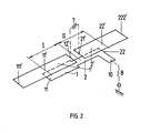
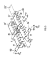
- Fig. 2,3,4,5,6 end 7 present its alternative realisations, only the wave guides being shown, with references 1,2 being used for input waveguides, and references 1', 2' for output waveguides.
- the balun consists of two second-order reactance sections I and II of electrical lengths equal to about a quarter of the wavelength of a radio- frequency signal.
- Each section I, II comprises two microstrip-like wave guides, the upper and lower one, whereof one, the lower one, is placed on the top side of a lower bottom metallized structure 3.
- the second guide, the upper one, placed above the first one, is separated therefrom by the material volume of the upper layered substrate 4.
- a pair of guides, any one from each section, is the input pair. For example, it is the pair of lower guides 1, 2 placed on the top side of the lower substrate 3.
- the guides being the input pair are connected with each other directly with the opposite internal ends.
- the external end 11 of one of the said guides is connected to the input port 10 through the intermediary of the transmission line 9 of the characteristic impedance Z o , while the other end 22 is open.
- the pair of the remaining guides 1', 2' being the output pair, forms with the op- posite internal ends thereof 12', 21 the balanced terminals of the output port 20.
- the balun design is realised alternatively depending on the selected method of terminating the ends 11', 22' of the pair of output guides and the end 22 of the pair of input guides, whereby there are, in general, the opposite phase terminations like, for example, short-circuit and opening to the ground.
- the external ends 11', 22' of the pair of output guides are both for direct current end for RF signal directly short-circuited to the ground, while the end 22 of the pair of input guides, opposite to the input port 10 is open.
- the external ends 11', 22' of the pair of output guides are short-circuited to the ground only for RF signal through the intermediary of quarter-wave segments of lines open at the ends at points 111', 222'.
- the external ends 11', 22' of the pair of output guides are short-circuited to the ground for RF signal through the intermediary of sufficiently large capacitances 5,5.
- the end 22 of the pair of input waveguides, opposite to the end 11 connected with the input port 10 is open for RF signal.
- balun in Fig.4 presents a circuit with the pair of input guides short-circuited to the ground in the point 11 and open external ends 11', 22' of the pair of output guides.
- This balun transformer option can achieve a dipole antenna performance when instead of the balanced load 7 the open space is considered.
- the balun is loaded with the load 7 of impedance R L either in the form of a lumped balanced load or in the form of a pair of unbalanced loads of impedances R L /2.
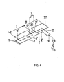
- the example of application of the balun for a double-balanced mixer design is presented in Fig. 5.
- the said mixer consists of two baluns connected with each other with pairs of balanced terminals of outputs 20 and 20 through the intermediary of a quad of diodes 30 in such a way that each of the baluns is connected to a different one of the two diagonals of the ring of diodes forming the quad 30.
- One of the baluns serves for supplying the RF power from the unbalanced input 101 to the quad, end the other one - for supplying the RF power of heterodyne from the unbalanced input 102.
- the ends of pairs of input guides 22 and 22 of both baluns, opposite to the inputs, are open to the ground.
- the external ends of pairs of output guides 11', 22' of both baluns are, on the other nand, short-circuited to the ground for RF signals, whereby for one of them the ends are short-circuited galvanically, and for the other one the said ends are short-circuited through the intermediary of sufficiently large capacitances 5, 5 or quarter-wave segments of transmission lines open on ends 111', 222' in order to collect the intermediate frequency (IF) product from the quad of diodes to the balanced TF output port 40,40.
- IF intermediate frequency
- the IF output port is connected to terminals of the output 20 of the signal balun through the intermediary of in-series inductances 6,6 which together with capacitances 5,5 or quarter-wave segments of open waveguides form low-pass filters 50, 56.
- the said filters determine the intermediate-frequency broadband properties of' the mixer.
- the said limit is considerably weaker for the example of the mixer in Fig.6.
- the said mixer differs from the previous one in that, in the signal balun,short-circuits are replaced by open-circuits and open-circuits are replaced by short- circuits to the ground.
- the end 221 of the .pair of input guides is directly short-circuited to the ground and the ends 111' and 221' of the pair of output guides are open-circuited to the ground.
- the low-pass filter used in the said mixer can have a wider IF band than in the previous mixer. Besides, the said mixer satisfies the sometimes imposed requirement that possible undesired input signals in the IF band are to be short-circuited at the signal input port of the mixer.
- the presented examples do not exhaust the advantageous possibilities of forming other systems of mixers with. the use of the balun according to the invention but they demonstrate its applications flexibility due both to its topological characteristics and the mutually complementary realisations.
- the balun operation consists in supplying full RF power from an unbalanced input port having input impedance 8 (Z o ) to a balanced output port having output impedance 7 close to R L or to a pair of unbalanced output ports having output impedance close to. RL/2, with equal amplitudes and the opposite phases at a possibly wide transmission band and possibly the best matching of input- and output ports.
- the balun design may be manufactured. with the use of the thin-film technology as in microwave hybrid integrated circuits on an alumina substrate (Al 2 O 3 ) 3 of thickness of from 0.50 up to 1.50 mm.
- the dielectric layer of the upper -substrate 4 separating the balun wave guides is made of a dielectric material which dielectric constant is close to the dielectric constant of the lower substrate 3 and the thickness equal to about 1/5 of the thickness of the lower substrate 3.
- the thickness of the upper substrate 4 is dependent on the required compensation ratio of the dispersion properties of wave guides.
- the balun is manufactured with the use of the monolithic technology proper to the monolithic integrated circuits on the substrate 3 of semi-insulating gallium arsenide GaAs of the thickness smaller than 0.50 mm.
- the dielectric layer of the upper substrate 4 separating the wave guides is made of silicon nitride Si 3 N 4 of thickness equal to about 1/5 of the thickness of the lower substrate 3.
- the balun design according to the invention is applicable especially as a 180° power divider, and in co-operation with a second balun and a quad of semiconductor diodes - as a double-balanced mixer or modulator.
- the above applications do not exhaust all possibilities created by the balun according to the invention. They have a very advantageous characteristic in the form of broadband properties, which can exceed even three octaves.
- the advantageous layered structure of the balun design with maintenance of the undisturbed bottom metallized ground plane suitable both for thin-film technology based on alumina substrate (Al 2 O 3 ), as well as for the monolithic technology utilizing semi-insulating gallium arsenide GaAs and a Si 3 N 4 layer.
- the monolithic realisation creates also the possibility of 'producing by selective epitaxy or ion implantation the semiconductor junctions directly in the substrate material of the balun used, for example, for a monolithic mixer design.
- the balun design according to the invention is appropriate for utilization within the frequency range of 1-18 GHz, i.e. within the range characteristic for wide applications of microstrip lines. Within the range of frequencies lower from the S band it is inferior to lumped baluns utilizing ferrite cores, whereas for the frequencies above 18 GHz - to fin-line and slot-line baluns superior to it in respect of easy combining with waveguide technique.
Abstract
Description
- The subject of the invention is a microwave balun for mixers and modulators using TEM wave guides in microstrip realisation.
- The balun is an electrical circuit transmitting radio frequency (RF) signal from an unbalanced input to a balanced output with minimum losses, whereby a broad transmission band and a high impedance transformation ratio are desireble as much as possible. The balun can be applied not only for a balanced load but also for a balanced pair of unbalanced outputs on which RF signals have equal amplitudes but opposite phases.
- The balun is a unit which forms an integral part of microwave balanced systems such as mixers, modulators, attenuators, switches and others, or a self-cantained unit supplying RF signal to balanced loads or inputs or outputs of balanced systems. The mentioned types of systems are very often produced using microstrip lines technique which enables integration thereof in the form of hybrid-or monolithic integrated circuits. This is the consequence of the property of microstrip lines which consists in concentrating the field of electromagnetic wave in the volume under the surface of the strip at a considerable shortening of wavelength in the dielectric substrate and in maintaining planarity of' the structure with an easy access to the top surface of the circuit for hybrid attached elements, while the bottom side is fixed as a ground plane. Therefore, it is desirable that the postulate of the microstrip type structure of the circuit should be maintained as close as possible.
- From among the hitherto applied baluns two should be distinguished, whereof one is the widely known Marchand's balun, and the other one is the Mouw's balun according to the U.S. patent specification no. 3,818,385.
- The Marchand's balun consists of two sections. Each section is composed of two coaxial lines, whereof one is placed coaxially in the other. Both sections are connected with each other by external conductors of the external lines. The internal lines are established by two quarter-wave sections of the inner coaxial lines, whereby tneir internal conductors are connected with etch other in the middle and inside of the balun and one of their ends is connected to the input external coaxial line, while the other end remains open to the ground. The internal ends of the external conductors of the said lines are connected to the balanced external output line leading to the balanced load outside the circuit, while their external ends are short--circuited to the ground. The Marchand's balun ex- cellently meets functional requirements both with respect to broadband and to impedance transformation ratio properties. Its transmission band can exceed even three octaves at loads selected from the range of from 50 Ohm up to 200 Ohm. It is one of the oldest microwave circuits of this type still being applied and permanently improved, It is widely applied for feeding the broadband symmetric antennas. It is, however, inapplicable in the balanced systems mentioned previously for the reason of its coaxial type structure and relatively large dimensions, especially if the cross-section is considered. The application thereof compels to use the coaxial type wave guides for systems directly co-operating therewith, which is not always acceptable, and certainly inconsistent with the demand of integration of systems.
- The Mouw's balun, improved by Hallford and described in the article "A Designer's Guide to planar Mixer Belun" published in Microwaves Dec 1979 pp. 52-57, is a relatively recent design. It consists of three conductive striplines, whereof one - the input one, is formed on the top side of the dielectric substrate, and the other two - the output ones - placed thereunder, are formed on the bottom side of the substrate. The external ends of the output lines are short-circuited to the ground which is established by contiguous matal- lization plane on the bottom side of the substrate. The Mouw's balun has more applications in balanced systems than the Marchand's balun design. It partially meets the planarity requirement, owing to the fact that it is somewhat closer to the microstrip type structure. Although its broadband and transformation properties do not come up to those of
- Marchand's design, they are sufficiently good for the needs of designing the broadband performance systems exceeding one octave.
- The drawback thereof is, however, the necessity of using the lines on both sides of the substrate, as a result of which the system cannot have one side bottom fixed to the ground. Since Mouw's design can offer a limited choice of the cross--section dimensions, and in consequence thereof, obtaining the desired performance, it can be applied only for few selected types of balanced systems.
- Among other examples not mentioned above, there is a rat race hybrid coupler called also a 180° hybrid, which meets the requirement of both microstrip type structure and the equal division of RF signal into two outputs in opposite phases, but its frequency band achieves only 20-30% of the mid--band frequency, and the possibilities of its matching in a wide load impedance range, are small. Moreover, it has the drawback of inconvenient arrangement of output ports, which hinders using .thereof for one balanced load, and its applications are limited to a balanced pair of unbalanced outputs.
- The above-discussed examples do not exhaust the existing types of realisation of balun designs but show the already disclosed trend to differentiate considerably the used wave guides from the desired microstrip type, e.g. not only by using coaxial lines but also coplanar-lines, or suspended-lines, or slot-lines, or fin-lines. Realisations of balanced systems in these techniques are plentiful but require forming the system either on both sides of the substrete or on one side thereof, nevertheless, they are always characterized by the impossibility of one side bottom fixing the circuit to the ground because the volume, beyond the dielectric substrate on both sides thereof and limited by the housing, is an integral part of the wave guide. Such systems are of great practical importance for structures combined with the waveguide technique but they are not suitable for integration.
- The aim of the invention is to provide a microwave balun circuit which can permit increased integration scale of microwave integrated circuits.
- The microwave balun design according to the invention consists of two second-order reactance sections of electrical lengths equal to about a quarter of the wavelength of a radio-frequency signal.. Each section comprises two microstrip-like wave guides placed in such a way above the ground plane being the bottom metallization of the lower layered substrate that one of the guides is on the top side of the lower substrate and the other guide, placed thereabove, is separated therefrom by the material of the upper layered substrate and is on the top side of the upper substrate.
- The pair of guides, any one from each section, being the pair of input guides, is connected vith each other by two ends, and one of the remaining ends thereof is connected to the input, while the other end is terminated f'or the radio-frequency signal by a reflecting element.
- The second pair of the remaining wave guides, being the pair of output guides, forms with its ends, one from each section, a pair of output-port terminals, while each of the remaining ends of the pair of output guides is terminated for the radio--frequency signal by a reflecting element. Phases of reflecting elements terminating the ends of output guides are dependent on the configuration choice of input- and output-ports and on the phase choice of the reflecting element terminating the end of input guides, the opposite to the input-port of the balun.
- The cross-section dimensions, in general different for each section and different for particular segments of each section, and material constants of the used materials have values dependent on the required broadband properties according to the set of transmission-reflection parameters of the balun design and the required input- and output-impedance.
- The terminals of the balanced output-port of the balun are loaded with a balanced load connected either directly or through the intermediary of a balanced transmission line, preferably as short as possible. Optionally, the terminals of the balanced output-port are loaded with a pair of unbalanced loads connected either directly or through the intermediary of unbalanced transmission lines, preferably as short as possible.
- In still another solution the terminals of the balanced output-port are loaded with electronically controlled elements or assembly of elements, connected either directly or through the intermediary of transmission lines, preferably as short as possible.
- On the other hand, in the monolithic realisation of this solution at least a part of a segment of any of the wave guides in the balun is enhanced either by lumped or by distributed semiconductor junctions.
- Reflecting elements in the balun according to the invention are either electronically controlled elements or unbalanced inputs of external reflecting systems connected directly or through the intermediary of transmission lines.
- The terminals of the balanced output-port of the balun are optionally loaded with a balanced output port of another balun design. The said load is connected directly or through the intermediary of electronically controlled elements or assembly of elements and/or through the intermediary of transmission lines, preferably as short as possible, thus forming systems of an in-series-, cross- or ring structure.
- The balun design according to the invention shows a number of advantages. Nemely, it precisely meets the postulate of a planer microstrip-like type structure. It meets the requirements of broadband performance up to three octaves inclusive over a wide range of impedance transformation ratio. Moreover, it has topologically advantageous location of output-port terminals, due to which it enables simple application both for a lumped balanced load and for a balanced pair of unbalanced output ports. It enables also complementary realisation by replacing the short-circuited to ground ends by open ended ones, and open ones by short-circuited ones, which is of significance for co-operation with different application systems. It is a geometrically compact and area saving design, due to which it minimizes the values of parasitic reactance elements.
- The presented balun design is especially convenient for production both with the use of thin--film- and monolithic technology, and moreover, it has relatively small dimensions and occupies small area, due to which it creates new possibilities of considerably large integration scale of complex balanced microwave systems, especially mixers and modulators.
- The subject of the invention will now be explained in more detail by reference to an example of its realisation in the drawing, in which Fig.1 presents one design of the balun, and Fig. 2,3,4,5,6 end 7 present its alternative realisations, only the wave guides being shown, with
references - The balun consists of two second-order reactance sections I and II of electrical lengths equal to about a quarter of the wavelength of a radio- frequency signal. Each section I, II comprises two microstrip-like wave guides, the upper and lower one, whereof one, the lower one, is placed on the top side of a lower bottom metallized structure 3. The second guide, the upper one, placed above the first one, is separated therefrom by the material volume of the upper
layered substrate 4. A pair of guides, any one from each section, is the input pair. For example, it is the pair oflower guides external end 11 of one of the said guides is connected to theinput port 10 through the intermediary of thetransmission line 9 of the characteristic impedance Zo, while theother end 22 is open. The pair of the remaining guides 1', 2', being the output pair, forms with the op- posite internal ends thereof 12', 21 the balanced terminals of theoutput port 20. The balun design is realised alternatively depending on the selected method of terminating the ends 11', 22' of the pair of output guides and theend 22 of the pair of input guides, whereby there are, in general, the opposite phase terminations like, for example, short-circuit and opening to the ground. For example, as in Fig.1, the external ends 11', 22' of the pair of output guides are both for direct current end for RF signal directly short-circuited to the ground, while theend 22 of the pair of input guides, opposite to theinput port 10 is open. In another example, as in Fig.2, the external ends 11', 22' of the pair of output guides are short-circuited to the ground only for RF signal through the intermediary of quarter-wave segments of lines open at the ends at points 111', 222'. In still another example, as in Fig.3, the external ends 11', 22' of the pair of output guides are short-circuited to the ground for RF signal through the intermediary of sufficientlylarge capacitances end 22 of the pair of input waveguides, opposite to theend 11 connected with theinput port 10, is open for RF signal. - The example of realisation of the balun in Fig.4 presents a circuit with the pair of input guides short-circuited to the ground in the
point 11 and open external ends 11', 22' of the pair of output guides. This balun transformer option can achieve a dipole antenna performance when instead of thebalanced load 7 the open space is considered. In all examples the balun is loaded with theload 7 of impedance RL either in the form of a lumped balanced load or in the form of a pair of unbalanced loads of impedances RL/2. - The example of application of the balun for a double-balanced mixer design is presented in Fig. 5. The said mixer consists of two baluns connected with each other with pairs of balanced terminals of
outputs unbalanced input 101 to the quad, end the other one - for supplying the RF power of heterodyne from theunbalanced input 102. The ends of pairs of input guides 22 and 22 of both baluns, opposite to the inputs, are open to the ground. The external ends of pairs of output guides 11', 22' of both baluns are, on the other nand, short-circuited to the ground for RF signals, whereby for one of them the ends are short-circuited galvanically, and for the other one the said ends are short-circuited through the intermediary of sufficientlylarge capacitances TF output port output 20 of the signal balun through the intermediary of in-series inductances capacitances pass filters 50, 56. The said filters determine the intermediate-frequency broadband properties of' the mixer. The said limit is considerably weaker for the example of the mixer in Fig.6. The said mixer differs from the previous one in that, in the signal balun,short-circuits are replaced by open-circuits and open-circuits are replaced by short- circuits to the ground. Thus, theend 221 of the .pair of input guides, the opposite one to theinput 101, is directly short-circuited to the ground and the ends 111' and 221' of the pair of output guides are open-circuited to the ground. The low-pass filter used in the said mixer can have a wider IF band than in the previous mixer. Besides, the said mixer satisfies the sometimes imposed requirement that possible undesired input signals in the IF band are to be short-circuited at the signal input port of the mixer. - The presented examples do not exhaust the advantageous possibilities of forming other systems of mixers with. the use of the balun according to the invention but they demonstrate its applications flexibility due both to its topological characteristics and the mutually complementary realisations. The balun operation consists in supplying full RF power from an unbalanced input port having input impedance 8 (Zo) to a balanced output port having
output impedance 7 close to RL or to a pair of unbalanced output ports having output impedance close to. RL/2, with equal amplitudes and the opposite phases at a possibly wide transmission band and possibly the best matching of input- and output ports. - For example, the balun design may be manufactured. with the use of the thin-film technology as in microwave hybrid integrated circuits on an alumina substrate (Al2O3) 3 of thickness of from 0.50 up to 1.50 mm. The dielectric layer of the upper -
substrate 4 separating the balun wave guides is made of a dielectric material which dielectric constant is close to the dielectric constant of the lower substrate 3 and the thickness equal to about 1/5 of the thickness of the lower substrate 3. The thickness of theupper substrate 4 is dependent on the required compensation ratio of the dispersion properties of wave guides. - In another design the balun is manufactured with the use of the monolithic technology proper to the monolithic integrated circuits on the substrate 3 of semi-insulating gallium arsenide GaAs of the thickness smaller than 0.50 mm. The dielectric layer of the
upper substrate 4 separating the wave guides is made of silicon nitride Si3N4 of thickness equal to about 1/5 of the thickness of the lower substrate 3. Such a realisation of the balun is especially convenient for microwave bands of above d GHz. - The cross-section dimensions, in general different for each section of wave guides and different for particular segments of each section, end dependent on the desired broad band properties for typically assumed impedances as e.g. 50 Ohm input and 100 Ohm load, show full feasibility of the design of the balun and considerable tolerance thereof to inaccuracy of technological processing. Noteworthy is the fact that feasibility of the balun design has no limitations in the selection of the cross-section dimensions of the sections which have appeared in other designs of baluns, whereby there is a certain degree of' freedom in the selection of both the material and the thickness of the upper substrate, which enables achievement of the desirable compensation of expected phase velocity ratio for even- and odd-mode excited waves up to full compensation thereof inclusive. In the consequence, the design of the balun gains a good technological feasibility, due to elimination of operations to correct the velocity ratio.
- The balun design according to the invention is applicable especially as a 180° power divider, and in co-operation with a second balun and a quad of semiconductor diodes - as a double-balanced mixer or modulator. The above applications do not exhaust all possibilities created by the balun according to the invention. They have a very advantageous characteristic in the form of broadband properties, which can exceed even three octaves. Besides, noteworthy is the advantageous layered structure of the balun design with maintenance of the undisturbed bottom metallized ground plane suitable both for thin-film technology based on alumina substrate (Al2O3), as well as for the monolithic technology utilizing semi-insulating gallium arsenide GaAs and a Si3N4 layer. The monolithic realisation creates also the possibility of 'producing by selective epitaxy or ion implantation the semiconductor junctions directly in the substrate material of the balun used, for example, for a monolithic mixer design.
- The balun design according to the invention is appropriate for utilization within the frequency range of 1-18 GHz, i.e. within the range characteristic for wide applications of microstrip lines. Within the range of frequencies lower from the S band it is inferior to lumped baluns utilizing ferrite cores, whereas for the frequencies above 18 GHz - to fin-line and slot-line baluns superior to it in respect of easy combining with waveguide technique.
Claims (15)
Applications Claiming Priority (2)
| Application Number | Priority Date | Filing Date | Title |
|---|---|---|---|
| PL1983245000A PL141094B1 (en) | 1983-12-09 | 1983-12-09 | Microwave balun transformer,especially for mixers and modulators |
| PL245000 | 1983-12-09 |
Publications (2)
| Publication Number | Publication Date |
|---|---|
| EP0146086A2 true EP0146086A2 (en) | 1985-06-26 |
| EP0146086A3 EP0146086A3 (en) | 1987-08-26 |
Family
ID=20019531
Family Applications (1)
| Application Number | Title | Priority Date | Filing Date |
|---|---|---|---|
| EP84114890A Withdrawn EP0146086A3 (en) | 1983-12-09 | 1984-12-07 | Microwave balun for mixers and modulators |
Country Status (7)
| Country | Link |
|---|---|
| US (1) | US4755775A (en) |
| EP (1) | EP0146086A3 (en) |
| JP (1) | JPS6121601A (en) |
| CS (1) | CS929284A2 (en) |
| HU (1) | HU192180B (en) |
| PL (1) | PL141094B1 (en) |
| SU (1) | SU1510726A3 (en) |
Cited By (5)
| Publication number | Priority date | Publication date | Assignee | Title |
|---|---|---|---|---|
| EP0213864A2 (en) * | 1985-08-31 | 1987-03-11 | Plessey Overseas Limited | Balun circuits |
| US6294965B1 (en) * | 1999-03-11 | 2001-09-25 | Anaren Microwave, Inc. | Stripline balun |
| KR100445243B1 (en) * | 2001-01-24 | 2004-08-21 | 가부시키가이샤 무라타 세이사쿠쇼 | Nonreciprocal circuit device and communication device |
| EP2432072A1 (en) * | 2010-09-21 | 2012-03-21 | Thales | Wideband balun on a multilayer circuit for a network antenna |
| WO2015094056A1 (en) * | 2013-12-19 | 2015-06-25 | Saab Ab | Balun |
Families Citing this family (29)
| Publication number | Priority date | Publication date | Assignee | Title |
|---|---|---|---|---|
| US4876744A (en) * | 1987-01-16 | 1989-10-24 | Matsushita Electric Industrial Co., Ltd. | Mixer with rat race circuit |
| US5025232A (en) * | 1989-10-31 | 1991-06-18 | Texas Instruments Incorporated | Monolithic multilayer planar transmission line |
| US5280647A (en) * | 1990-06-14 | 1994-01-18 | Taisei Co., Ltd. | Double-balanced mixer with triple-layer film transformers |
| US5125111A (en) * | 1990-09-04 | 1992-06-23 | Rockwell International Corporation | Resistive planar ring double-balanced mixer |
| DE4438809B4 (en) * | 1994-10-31 | 2004-11-04 | Rohde & Schwarz Gmbh & Co. Kg | Dipolspeiseanordnung |
| US5745017A (en) * | 1995-01-03 | 1998-04-28 | Rf Prime Corporation | Thick film construct for quadrature translation of RF signals |
| US5534830A (en) * | 1995-01-03 | 1996-07-09 | R F Prime Corporation | Thick film balanced line structure, and microwave baluns, resonators, mixers, splitters, and filters constructed therefrom |
| US5774801A (en) * | 1995-08-23 | 1998-06-30 | Ericsson Inc. | High dynamic range mixer having low conversion loss, low local oscillator input power, and high dynamic range and a method for designing the same |
| US5819169A (en) * | 1996-05-10 | 1998-10-06 | Northrop Grumman Corporation | High performance mixer structures for monolithic microwave integrated circuits |
| US5781078A (en) * | 1996-12-05 | 1998-07-14 | Glenayre Electronics, Inc. | Filter enhancement using input-to-output ground isolation and shielding |
| KR100223375B1 (en) * | 1997-06-11 | 1999-10-15 | 윤종용 | Apparatus and method for automatically contwlling gain in multic-channel communication system |
| US6201439B1 (en) * | 1997-09-17 | 2001-03-13 | Matsushita Electric Industrial Co., Ltd. | Power splitter/ combiner circuit, high power amplifier and balun circuit |
| US5970353A (en) * | 1998-03-30 | 1999-10-19 | Advanced Micro Devices, Inc. | Reduced channel length lightly doped drain transistor using a sub-amorphous large tilt angle implant to provide enhanced lateral diffusion |
| US6094570A (en) * | 1998-05-06 | 2000-07-25 | Northrop Grumman | Double-balanced monolithic microwave integrated circuit mixer |
| US6351192B1 (en) | 1999-03-25 | 2002-02-26 | Industrial Technology Research Institute | Miniaturized balun transformer with a plurality of interconnecting bondwires |
| US6133806A (en) * | 1999-03-25 | 2000-10-17 | Industrial Technology Research Institute | Miniaturized balun transformer |
| US6278340B1 (en) | 1999-05-11 | 2001-08-21 | Industrial Technology Research Institute | Miniaturized broadband balun transformer having broadside coupled lines |
| US6529090B2 (en) | 2001-05-15 | 2003-03-04 | Lockheed Martin Corporation | Two-sided printed circuit anti-symmetric balun |
| KR100715861B1 (en) * | 2006-02-17 | 2007-05-11 | 삼성전자주식회사 | Balun |
| JP5249508B2 (en) | 2006-11-06 | 2013-07-31 | 三菱重工業株式会社 | Track system |
| TWI351784B (en) * | 2008-05-29 | 2011-11-01 | Cyntec Co Ltd | Balun |
| JPWO2010055682A1 (en) * | 2008-11-14 | 2012-04-12 | 株式会社フジクラ | Resin multilayer device and manufacturing method thereof |
| US8354892B2 (en) * | 2009-11-03 | 2013-01-15 | Electronics And Telecommunications Research Institute | Marchand balun device for forming parallel and vertical capacitance |
| JP5427702B2 (en) * | 2010-06-11 | 2014-02-26 | パナソニック株式会社 | Unbalanced balance converter |
| US8868021B1 (en) | 2013-04-05 | 2014-10-21 | National Instruments Corporation | Ultra-broadband planar millimeter-wave mixer with multi-octave IF bandwidth |
| CN103474734B (en) * | 2013-08-20 | 2016-08-10 | 京信通信技术(广州)有限公司 | Electric bridge |
| US9692387B2 (en) * | 2015-07-24 | 2017-06-27 | Nxp Usa, Inc. | Balun transformer |
| CN113098451B (en) * | 2021-03-02 | 2022-11-04 | 电子科技大学 | Broadband microwave narrow pulse modulator based on double-balance structure |
| US11876278B2 (en) | 2021-03-29 | 2024-01-16 | Raytheon Company | Balun comprising stepped transitions between balance and unbalance connections, where the stepped transitions include ground rings of differing lengths connected by caged vias |
Citations (4)
| Publication number | Priority date | Publication date | Assignee | Title |
|---|---|---|---|---|
| US3845490A (en) * | 1973-05-03 | 1974-10-29 | Gen Electric | Stripline slotted balun dipole antenna |
| EP0022990A1 (en) * | 1979-07-20 | 1981-01-28 | Siemens Aktiengesellschaft | Microstrip microwave balun |
| US4330868A (en) * | 1980-12-15 | 1982-05-18 | Rockwell International Corp. | Balun coupled microwave frequency converter |
| GB2089135A (en) * | 1980-11-28 | 1982-06-16 | Marconi Co Ltd | Improvements in or relating to baluns |
Family Cites Families (28)
| Publication number | Priority date | Publication date | Assignee | Title |
|---|---|---|---|---|
| US2597853A (en) * | 1945-01-03 | 1952-05-27 | Us Sec War | Unbalanced to balanced line transformer |
| US2606964A (en) * | 1948-02-07 | 1952-08-12 | Rca Corp | Radio frequency transmission line circuits |
| US3222621A (en) * | 1961-01-28 | 1965-12-07 | Nippon Electric Co | Coupling device |
| US3497832A (en) * | 1967-08-24 | 1970-02-24 | Emerson Electric Co | Radio frequency transmission line tee hybrid |
| US3656071A (en) * | 1970-06-25 | 1972-04-11 | Rca Corp | Wide band balun |
| US3757342A (en) * | 1972-06-28 | 1973-09-04 | Cutler Hammer Inc | Sheet array antenna structure |
| US3818385A (en) * | 1972-09-21 | 1974-06-18 | Aertech | Hybrid junction and mixer or modulator |
| JPS51135351A (en) * | 1975-05-19 | 1976-11-24 | Matsushita Electric Ind Co Ltd | Frequency converter |
| US3991390A (en) * | 1975-07-31 | 1976-11-09 | Motorola, Inc. | Series connected stripline balun |
| US4052785A (en) * | 1975-11-28 | 1977-10-11 | Dana Corporation | Method of making a transformer assembly |
| US4032850A (en) * | 1976-01-12 | 1977-06-28 | Varian Associates | Coaxial balun with doubly balanced heterodyne converter |
| JPS5423447A (en) * | 1977-07-25 | 1979-02-22 | Toshiba Corp | Strip line coupling circuit |
| JPS5857001B2 (en) * | 1977-12-23 | 1983-12-17 | 三菱電機株式会社 | Push-pull conversion circuit |
| US4186352A (en) * | 1978-03-23 | 1980-01-29 | Rockwell International Corporation | Signal converter apparatus |
| US4193048A (en) * | 1978-06-22 | 1980-03-11 | Rockwell International Corporation | Balun transformer |
| US4288762A (en) * | 1978-09-26 | 1981-09-08 | The United States Of America As Represented By The Secretary Of The Navy | Wideband 180° hybrid junctions |
| US4276521A (en) * | 1978-12-18 | 1981-06-30 | Trw Inc. | Quadriphase integrated high-speed microwave modulator |
| US4245356A (en) * | 1979-04-27 | 1981-01-13 | Rockwell International Corporation | Frequency translator |
| JPS5635507A (en) * | 1979-08-31 | 1981-04-08 | Nec Corp | Double balanced frequency transducer |
| US4260963A (en) * | 1979-10-18 | 1981-04-07 | Rockwell International Corporation | 4:1 Balun |
| US4288759A (en) * | 1980-01-28 | 1981-09-08 | Stover Harry L | Microwave transformer |
| US4371982A (en) * | 1981-03-13 | 1983-02-01 | Rockwell International Corporation | Microwave frequency converter with economical coupling |
| US4375699A (en) * | 1981-03-13 | 1983-03-01 | Rockwell International Corporation | Microwave frequency converter with dual balun port |
| US4392250A (en) * | 1981-05-19 | 1983-07-05 | Rockwell International Corporation | Symmetric microwave mixer |
| US4359782A (en) * | 1981-05-19 | 1982-11-16 | Rockwell International Corporation | Microwave mixer with linking juxtaposed balun port |
| US4380831A (en) * | 1981-07-24 | 1983-04-19 | Rockwell International Corporation | Symmetric microwave mixer with improved isolation |
| US4392251A (en) * | 1981-07-24 | 1983-07-05 | Rockwell International Corporation | Symmetric microwave mixer with coplanar diode connection |
| US4399562A (en) * | 1981-07-24 | 1983-08-16 | Rockwell International Corporation | Full balun mixer |
-
1983
- 1983-12-09 PL PL1983245000A patent/PL141094B1/en unknown
-
1984
- 1984-11-28 SU SU843817577A patent/SU1510726A3/en active
- 1984-12-03 CS CS849292A patent/CS929284A2/en unknown
- 1984-12-04 US US06/677,847 patent/US4755775A/en not_active Expired - Fee Related
- 1984-12-06 HU HU844542A patent/HU192180B/en not_active IP Right Cessation
- 1984-12-07 EP EP84114890A patent/EP0146086A3/en not_active Withdrawn
- 1984-12-10 JP JP59261681A patent/JPS6121601A/en active Pending
Patent Citations (4)
| Publication number | Priority date | Publication date | Assignee | Title |
|---|---|---|---|---|
| US3845490A (en) * | 1973-05-03 | 1974-10-29 | Gen Electric | Stripline slotted balun dipole antenna |
| EP0022990A1 (en) * | 1979-07-20 | 1981-01-28 | Siemens Aktiengesellschaft | Microstrip microwave balun |
| GB2089135A (en) * | 1980-11-28 | 1982-06-16 | Marconi Co Ltd | Improvements in or relating to baluns |
| US4330868A (en) * | 1980-12-15 | 1982-05-18 | Rockwell International Corp. | Balun coupled microwave frequency converter |
Non-Patent Citations (1)
| Title |
|---|
| CONFERENCE PROCEEDINGS OF THE 14th EUROPEAN MICROWAVE CONFERENCE, 10th - 13th September 1984, Liège, BE, pages 166-171; W. MARCZEWSKI et al.: "The overlapped microstrip for MICs and MMICs" * |
Cited By (8)
| Publication number | Priority date | Publication date | Assignee | Title |
|---|---|---|---|---|
| EP0213864A2 (en) * | 1985-08-31 | 1987-03-11 | Plessey Overseas Limited | Balun circuits |
| EP0213864A3 (en) * | 1985-08-31 | 1988-09-07 | Plessey Overseas Limited | Balun circuits |
| US6294965B1 (en) * | 1999-03-11 | 2001-09-25 | Anaren Microwave, Inc. | Stripline balun |
| KR100445243B1 (en) * | 2001-01-24 | 2004-08-21 | 가부시키가이샤 무라타 세이사쿠쇼 | Nonreciprocal circuit device and communication device |
| EP2432072A1 (en) * | 2010-09-21 | 2012-03-21 | Thales | Wideband balun on a multilayer circuit for a network antenna |
| FR2965112A1 (en) * | 2010-09-21 | 2012-03-23 | Thales Sa | MULTI-LAYER CIRCUIT BROADBAND SYMETRISER FOR NETWORK ANTENNA |
| WO2015094056A1 (en) * | 2013-12-19 | 2015-06-25 | Saab Ab | Balun |
| US9583841B2 (en) | 2013-12-19 | 2017-02-28 | Saab Ab | Balun |
Also Published As
| Publication number | Publication date |
|---|---|
| EP0146086A3 (en) | 1987-08-26 |
| PL245000A1 (en) | 1985-07-02 |
| US4755775A (en) | 1988-07-05 |
| CS929284A2 (en) | 1991-02-12 |
| JPS6121601A (en) | 1986-01-30 |
| HUT37691A (en) | 1986-01-23 |
| SU1510726A3 (en) | 1989-09-23 |
| PL141094B1 (en) | 1987-06-30 |
| HU192180B (en) | 1987-05-28 |
Similar Documents
| Publication | Publication Date | Title |
|---|---|---|
| EP0146086A2 (en) | Microwave balun for mixers and modulators | |
| US4607394A (en) | Single balanced planar mixer | |
| Kormanyos et al. | CPW-fed active slot antennas | |
| US5142255A (en) | Planar active endfire radiating elements and coplanar waveguide filters with wide electronic tuning bandwidth | |
| US5265266A (en) | Resistive planar star double-balanced mixer | |
| US4032849A (en) | Planar balanced mixer/converter for broadband applications | |
| US4091343A (en) | Insular waveguide directional coupler | |
| Tahim et al. | Design and performance of W-band broad-band integrated circuit mixers | |
| US4097826A (en) | Insular waveguide ring resonator filter | |
| US7498897B2 (en) | Impedance matching circuit, and semiconductor element and radio communication device using the same | |
| EP1076935B1 (en) | Double-balanced monolithic microwave integrated circuit mixer | |
| US4641369A (en) | Local oscillator and mixer assembly | |
| US4430758A (en) | Suspended-substrate co-planar stripline mixer | |
| Chen et al. | A wide-band multiport planar power-divider design using matched sectorial components in radial arrangement | |
| US6198912B1 (en) | Frequency converter for the application on millimetric radio waves | |
| US3950703A (en) | Microcircuit reverse-phased hybrid ring mixer | |
| US4048589A (en) | Receiver module and components thereof | |
| Kwang et al. | 4× 4 Butler matrix beam forming network using novel reduced size branchline coupler | |
| Lin et al. | Tunable balanced power dividers: An overview of recently developed balanced power dividers and couplers with fixed and tunable functions | |
| US4328471A (en) | Bandwidth compensated quarter-wave coupled power combiner | |
| US4749969A (en) | 180° hybrid tee | |
| KR100471049B1 (en) | non-radiative dielectric waveguide mixer using a ring hybrid coupler | |
| US4072902A (en) | Receiver module and mixer thereof | |
| US4709410A (en) | Frequency conversion circuits | |
| KR19990000905A (en) | Frequency converters for use in microwave systems |
Legal Events
| Date | Code | Title | Description |
|---|---|---|---|
| PUAI | Public reference made under article 153(3) epc to a published international application that has entered the european phase |
Free format text: ORIGINAL CODE: 0009012 |
|
| AK | Designated contracting states |
Designated state(s): DE FR GB |
|
| PUAL | Search report despatched |
Free format text: ORIGINAL CODE: 0009013 |
|
| AK | Designated contracting states |
Kind code of ref document: A3 Designated state(s): DE FR GB |
|
| 17P | Request for examination filed |
Effective date: 19871008 |
|
| STAA | Information on the status of an ep patent application or granted ep patent |
Free format text: STATUS: THE APPLICATION IS DEEMED TO BE WITHDRAWN |
|
| 18D | Application deemed to be withdrawn |
Effective date: 19900703 |
|
| RIN1 | Information on inventor provided before grant (corrected) |
Inventor name: NIEMYJSKI, WACLAW Inventor name: MARCZEWSKI, WOJCIECH |