EP0150060B1 - Multifunctional image processor - Google Patents
Multifunctional image processor Download PDFInfo
- Publication number
- EP0150060B1 EP0150060B1 EP85100507A EP85100507A EP0150060B1 EP 0150060 B1 EP0150060 B1 EP 0150060B1 EP 85100507 A EP85100507 A EP 85100507A EP 85100507 A EP85100507 A EP 85100507A EP 0150060 B1 EP0150060 B1 EP 0150060B1
- Authority
- EP
- European Patent Office
- Prior art keywords
- image data
- gray
- data
- scale
- image
- Prior art date
- Legal status (The legal status is an assumption and is not a legal conclusion. Google has not performed a legal analysis and makes no representation as to the accuracy of the status listed.)
- Expired
Links
Images


Classifications
-
- G—PHYSICS
- G06—COMPUTING; CALCULATING OR COUNTING
- G06T—IMAGE DATA PROCESSING OR GENERATION, IN GENERAL
- G06T1/00—General purpose image data processing
- G06T1/20—Processor architectures; Processor configuration, e.g. pipelining
Definitions
- the present invention relates to an image processor of an image processing system, and in particular, to a multifunctional image processor suitable for executing various image processing functions at a higher speed.
- Image processing techniques in general, are classified into such processing steps as a preprocessing, a feature extraction, and an object recognition processing.
- a preprocessing there has been a system utilizing a general-purpose computer for selecting and executing various kinds of preprocessing to be applicable to general purposes and to be repeated in many cases by use of programs for the respective objects.
- the preprocessing cannot be achieved at a satisfactory speed by a series of operations: Fetching image data, executing a necessary arithmetic operation on the fetched image data, and storing the result of the operation again in a memory.
- a multifunctional image processor with the features set forth in the first part of claim 1 is known from COMPUTER DESIGN, Sept. 1979, pages 93-101. Although this processor permits rapid execution of parallel processing, its hardware possesses only dedicated functions, hence it has been impossible to process various functions by a single processor at a high speed required for above-stated processing.
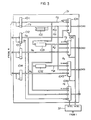
- a control processor 1 for controlling the overall system comprises a general-purpose microprocessor and supplies various instructions through a system bus 6 to an address processor 2 and a multifunctional image processor 3 of the present invention, thereby achieving various image processing. These instructions are determined depending on programs in the control processor 1, hence the image processing in this system can be regarded as programmable in this regard.
- the address processor 2 for executing an access control on an image memory 4 fetches an image to be processed via an address bus 7 and carried out an addressing operation for storing an image resulting from the image processing based on the instructions.
- the image memory 4 is connected to an image monitor 9 for displaying image data and an industrial television camera 8 for shooting an object to obtain an image thereof in this embodiment.
- the image data supplied from the image memory 4 to the multifunctional image processor 3 primarily comprises gray-scale image data F, and color image data G (green), B (blue), and R (red).
- the image memory 4 is constructed with maximum four planes (to be referred to as channels hereinbelow) of image memory units (assigned with channel numbers 0 to 3) in which the gray-scale image data F is stored in the image memory unit associated with channel number 0 and the color image data G, B, and R are stored in the image memory units associated with channel numbers 1, 2, and 3, respectively.
- the image memory 4 supplies the multifunctional image processor 3 with the image data to be processed including the gray-scale image data F and color image data G, B, and R.
- image data H obtained as a result from a processing conducted by the multifunctional image processor 3 is outputted to the image memory 4 and can be stored in an image memory unit associated with an arbitrary channel number (0 to 3) under control of the address processor 2.
- a gray-scale density frequency distribution of the output image data H, an X/Y projection distribution, and the like are obtained by use of a histogram processor 5.
- the data on each channel of the image memory 4, that is, the image data F, G, B, R, and H, is each comprised with 8-bit gray-scale data and 1-bit binary data.
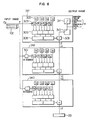
- the multifunctional image processor 3 receives image data F, G, B, R inputted from the image memory 4 depicted in Fig. 1, performs various kinds of image processing, and outputs the image data H.
- This image processor 3 comprises an image data distribute circuit 31 and a parallel image data processing circuit 32.
- the image data processing circuit 31 receives image data F, G, B, and R and distributes to the paralleled image data processing circuit 32 at the subsequent stage image data in a form corresponding to an instruction set to an instruction register 37 of an input image by the control processor 1.
- the parallel image data processing circuit 32 comprises three image signal processors (ISP) each configured in a large scale integration circuit and connected in the circuit 32.
- ISP image signal processors
- the respective ISP's 341-343 process data inputted from the image input ports A, B and LI, respectively and delivers a result of the processing to an output port LO.
- Data from a data register (DR) 36 is fed to port Ll of the ISP 343 at the first stage and an image data H comprising 8-bit gray-scale data and 1-bit binary data is outputted as the final result from the port LO of ISP 341 at the last stage.
- Part of the operations of the processing in the ISP's 341-343 and input image data are determined by setting data such as a weighting coefficient from the control processor 1 to an address register (AR) 36, by loading data in the data register (DR) 36, and by supplying a control signal, FUN of an operation function to each ISP.
- AR address register
- the registers 1011-1014 for latching the image data F, G, B, and R inputted to the image data distribute circuit 31 are respectively so configured that the 8-bit gray-scale data and the 1-bit binary data can be separately fetched.
- gray-scale image data F includes gray-scale data Fg and binary data Fb and that the color image data G, B, and R contain the gray-scale data Gg, Bg, and Dg, respectively of color information and the binary data Gb, Bb, and Rb, respectively.
- a delay circuit 102 processes the binary data Fb of the gray-scale image data F and outputs seven data signals obtained by delaying the binary data Fb by one line to seven lines in terms of lines on the screen.
- the binary data Fb and delayed signals are represented to be Fb o to Fb 7 , respectively.
- Delay circuits 1031 and 1032 are serially connected and each supplies a delay to the gradation data Fg of the gradation image data F by the one-line step, so the outputs therefrom are delayed by one line and two lines, respectively and are represented as Fg, and Fg 2 , respectively.
- Selectors 1041-1044 each is disposed to select one of four inputs so as to determine inputs to ports A and B of the ISp's 341-343 of the parallel image data processing circuit 31.
- selectors 1041-1043 the inputs assigned with the same input number are selected in accordance with a port select signal ASEL(n) loaded in an instruction register 37, then the selected signal is transmitted to the port A of each ISP 341-343 in the parallel image data processing circuit 32.
- a selector 1044 performs a signal selection in accordance with a port B select signal BSEL(n) set to the instruction register 37 and the selected data is sent to the port B of each ISP 341-343.
- the value n ranges from one to n and the inputs whose input numbers match with those assigned to the selectors 1041-1044, respectively of Fig. 3 are selected. (Refer to Table 1 for details about the select operation).
- the image data associated with the operation of the image processing can be inputted to each ISP by use of programs by appropriately setting ASEL(n) and BSEL(n) in accordance with instructions from the control processor 1.
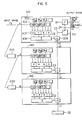
- Each ISP 341-343 of Fig. 2 has the same configuration, which is depicted in Fig. 4.
- the SIP is an LSI circuit for image processing and which has been disclosed in the Japanese Patent Laid-Open No. 59-146,366 (EP-A-0118053) and comprises the following units.
- EP-A-0118053 Japanese Patent Laid-Open No. 59-146,366
- Z3 or Z4 is delivered from a port LO, while as the binary data, the resultant binary value from the BU 311 is outputted from a port BO.
- those from the port LO are determined by the register number specification obtained from the address register (AR) 36 through a port MRA.
- the concrete data of the signal FUN is listed in Table 2.
- the signal FUN comprises eight signals as represented in the table in which IFUN is a signal for selecting the Y input of the PE 305; ADLY and BDLY are signals for specifying the number of delay stages of the variable-stage shift registers 301 and 304, respectively, PEFUN and PEINH are signals for specifying an operation of the PE 305, and AUFUN, LUFUN, and OUFUN are signals for specifying operations of the AU 308, LU 309, and OU 310, respectively.
- a variety of image processing operations can be executed by supplying the above-stated image data distribute circuit 31 and the parallel image data processing circuit 32 with appropriate control signals and data by use of programs of the control processor 1.
- Fig. 5 illustrates the first example in which the spatial convolution is carried out.
- the gray-scale data Fg of the gray-scale image data is used for this operation.
- the ASEL (2) is specified as the port A select signal in the instruction register 37 for the selectors 1041-1043 of the image data distribute circuit 31 and that ADLY(0) specifies the number of the delay stages associated with port A for the ISP's 341-343 of the parallel image data processing circuit 32.
- Fg, Fg,, and Fg 2 are obtained as the port A inputs to the ISP's 341-343 from Table 1.
- an array of the gray-scale data Fg of the gray-scale image data on the screen is configured with L (rows) by M (columns) pixels as depicted in Table 3.
- each pixel data f LM comprises eight bits as described before.
- the shift register 303 in the ISP transfers the data to the right with a 1-pixel delay.
- a 1-line delay (a M-pixel delay in the example of Table 3) is provided by delay circuits 1031 and 1032 in the image data distribute circuit 31, hence at a point where f 11 , f 12 , and f 13 are set to the shift register 303 of the ISP 343 via port A as illustrated in Fig.
- the input function which is the Y input select signal of the PE 305 is IFUN (1)
- the PE function which is the signal for specifying the operation of the PE 305 is PEFUN (1)
- the PE inhibit is indicated by PEINH (1, 1, 1, 2).
- Table 2 the contents of the RAM described above and the content of the register 303 obtained from port A are inputted to three PE's 305 disposed on the left, and the products therebetween are outputted as Z 11 to Z 13 .
- the port B input does not affect the circuit operation in this situation, that is, the port B select signal BSEL (n) and BDLY (n) which specifies the number of delay stages for port B need not be specified; furthermore, the output from the right-most PE is forcibly set to zero, hence the RAM 302 and register 303 associated with the PE do not affect the circuit operation, either.
- AUFUN (1) is specified to each ISP as a signal for indicating an operation of the arithmetic unit (AU) function
- the AU 308 calculates the sum of products of each PE 305 described above as follows:
- the LUFUN (1) is specified for each ISP as a signal for indicating an operation of the linkage unit (LU) function
- OUFUN (3, N) is specified for the ISP's 342 and 343 are signals for indicating an operation of the output unit (OU) function
- OUFUN (1, N) is specified for the ISP 341.
- each ISP adds an input Z21 from port L1 and each Z2 obtained from expression (1)
- the data register 35 is beforehand set to zero
- the output Z3 from the LU 309 of the ISP 341 is represented as the sum of each Z2 of expression (1).
- the ISP 341 outputs via the OU 310 to the image memory 4 image data H comprising gray-scale data undergone N-bit shift down and binary data obtained therefrom.
- expression (2) represents the results of the arithmetic operation of expression (1) when the first three pixels in lines 1, 2, and 3 are set to the register 303 of Fig. 5.
- the output Z3 is represented as follows because the register 305 of each ISP contains the pixel data: (f 34 , f 33 , f 32 ) for the ISP 341, (f 24 , f 23 , f 22 ) for the ISP 342, and (fi4, f 13 , f 12 ) for the ISP 343
- Z3 is obtained as: This means that the sum of products is sequentially calculated for the 3 by 3 pixels comprising the (y + 1)-th, (y + 2)-th,and(y + 3)-th pixel data of lines x + 1, x + 2, and x + 3.
- this arithmetic operation can be advantageously applicable to image processing such as noise reduction and edge emphasis.
- OUFUN (1, N) to the OU 310 of the ISP 341 is replacecd with OUFUN (2, N) (with other conditions retained)
- a signal resulting from an execution of an N-bit shift down conducted on the absolute value of Z3 represented by expression (4) is obtained as an output as will be seen from the contents of Table 2.
- the second example is a modification of the above-stated spatial convolution in which another operation can be executed only by changing control signals.
- This example represents arithmetic operations for calculating the maximum and minimum values.
- control signals of the first example PEFUN (2), AUFUN (2), and LUFUN (2) are assumed to indicate instructions for the PE 305, AU 308, and LU 309 of each ISP.
- LUFUN (2) and AUFUN (2) are replaced with LUFUN (3) and AUFUN (3), respectively, the minimum value as represented by
- Fig. 6 illustrates the state of each unit when the program specifications are made as follows: IFUN (2), ADLY (0), BDLY (1), PEFUN (6), AUFUN (2), LUFUN (2), OUFUN (1, 0), and PEINH (1, 1, 1, 3) for each ISP, and ASEL (2) and BSEL (2).
- the maximum value is obtained as:
- edge emphasis function is implemented. If PEINH (3, 1, 3, 3), PEINH (1, 3, 1, 3), and PEINH (3, 1, 3, 3) are specified for the ISP's 341-343, expression (6) can be executed only at the center of the 3 by 3 pixels and in four directions thereof (upper, lower, right, and left directions).
- Fig. 7 illustrates the state of each unit when ASEL (4) is specified to the selectors 1041-1043 in the image data distribute circuit 31 and the program specifications IFUN (1), ADLY (0), PEFUN (1), AUFUN (1), LUFUN (1), OUFUN (1, 0), and PEINH (1,2,2,2) are made to each ISP, hence the following operation is carried out: where a, ⁇ , and y are coefficients loaded in the RAM 302 of the ISP. This function is used to convert a color image into a monochrome image. It can be further applicable to the operations described below by changing PEFUN, AUFUN, and LUFUN.
- Fig. 8 represents a binary-value pattern matching operation in which the binary data F 60 to F 67 of the gray-scale image data F are used.
- Fig. 8 depicts the state of each unit when ASEL (3) is specified for the selectors 1041-1043 of the image data distribute circuit 31, the program specifications IFUN (1), PEFUN (13), AUFUN (1), LUFUN (1), OUFUN (1, 0), and PEINH (1, 1, 1, 1 ) are made to each ISP, and ADLY (0), ADLY (4), and ADLY (8) are specified for the ISP's 341, 342, and 343, respectively. In this case, the following operation is achieved.
- P 12 represents a binary data of eight vertical pixels on the screen because the binary data F b is delayed by one line to seven lines in the delay circuit 102, while P 11 to P, are obtained by delaying the binary data F b by one pixel to 11 pixels.
- a binary image comprising 8 (vertical) by 12 (horizontal) pixels on the screen is stored as P 12 to P, in the shift register 303, hence the pattern matching between these data items and the template signals t l2 to t, stored in the RAM 302 can be implemented.
Description
- The present invention relates to an image processor of an image processing system, and in particular, to a multifunctional image processor suitable for executing various image processing functions at a higher speed.
- Image processing techniques, in general, are classified into such processing steps as a preprocessing, a feature extraction, and an object recognition processing. For the preprocessing, there has been a system utilizing a general-purpose computer for selecting and executing various kinds of preprocessing to be applicable to general purposes and to be repeated in many cases by use of programs for the respective objects. However, the preprocessing cannot be achieved at a satisfactory speed by a series of operations: Fetching image data, executing a necessary arithmetic operation on the fetched image data, and storing the result of the operation again in a memory.
- In the field of image processing (preprocessing), on the other hand, there are a lot of arithmetic operations to be executed on image data items existing close to each other, for example, in a special convolution for implementing the noise reduction and contour extract functions, that is, a parallel processing is required to be executed on local data items in many cases.
- A multifunctional image processor with the features set forth in the first part of
claim 1 is known from COMPUTER DESIGN, Sept. 1979, pages 93-101. Although this processor permits rapid execution of parallel processing, its hardware possesses only dedicated functions, hence it has been impossible to process various functions by a single processor at a high speed required for above-stated processing. - It is therefore an object of the present invention to provide a multifunctional image processor which is capable of executing various image processing (preprocessing) in realtime or at a higher speed.
- This object is met by the invention as characterized in
claim 1, which permits various kinds of data processing configurations and operation functions to be specified by the use of programs, so that a single image processor is enabled to execute many image processing functions at a higher speed. - While the use of grey-scale image data delay means for generating a plurality of delayed grey-scale image data in a high speed convolution system is known from PRIP 82 - PROCEEDINGS OF THE IEEE COMPUTER SOCIETY CONFERENCE ON PATTERN RECOGNITION AND IMAGE PROCESSING, Las Vegas, Nevada, USA, June 14 to 17,1982, pages 390-392, that document again does not disclose select means for selecting the image data in accordance with an external signal, so that it does not achieve the advantageous effect of the invention set forth above.
- The objects and features of the present invention will become more apparent from the consideration of the following detailed description taken in conjunction with the accompanying drawings in which:
- Fig. 1 is a schematic block diagram illustrating a system configuration example utilizing a multifunctional image processor of the present invention;
- Fig. 2 is a circuit block diagram illustrating an embodiment of a multifunctional image processor of the present invention;
- Fig. 3 depicts an example of an image data distribute circuit;
- Fig. 4 illustrates a configuration example of a parallel image data processing circuit;
- Fig. 5 is a schematic diagram for explaining an example of image processing in which the spatial convolution is executed;
- Fig. 6 illustrates a schematic block diagram for explaining an example of image processing in which a nonlinear neighborhood operation is carried out;
- Fig. 7 is a block diagram illustrating an example of image processing in which color images are processed; and
- Fig. 8 is a schematic diagram demonstrating an example of image processing in which a pattern matching operation is conducted on binary images.
- In the following paragraphs, the present invention will be described in conjunction with embodiments thereof. Referring to Fig. 1, a
control processor 1 for controlling the overall system comprises a general-purpose microprocessor and supplies various instructions through asystem bus 6 to anaddress processor 2 and amultifunctional image processor 3 of the present invention, thereby achieving various image processing. These instructions are determined depending on programs in thecontrol processor 1, hence the image processing in this system can be regarded as programmable in this regard. Theaddress processor 2 for executing an access control on animage memory 4 fetches an image to be processed via an address bus 7 and carried out an addressing operation for storing an image resulting from the image processing based on the instructions. Theimage memory 4 is connected to animage monitor 9 for displaying image data and anindustrial television camera 8 for shooting an object to obtain an image thereof in this embodiment. The image data supplied from theimage memory 4 to themultifunctional image processor 3 primarily comprises gray-scale image data F, and color image data G (green), B (blue), and R (red). Theimage memory 4 is constructed with maximum four planes (to be referred to as channels hereinbelow) of image memory units (assigned withchannel numbers 0 to 3) in which the gray-scale image data F is stored in the image memory unit associated withchannel number 0 and the color image data G, B, and R are stored in the image memory units associated withchannel numbers image memory 4 supplies themultifunctional image processor 3 with the image data to be processed including the gray-scale image data F and color image data G, B, and R. - On the other hand, image data H obtained as a result from a processing conducted by the
multifunctional image processor 3 is outputted to theimage memory 4 and can be stored in an image memory unit associated with an arbitrary channel number (0 to 3) under control of theaddress processor 2. At the same time, a gray-scale density frequency distribution of the output image data H, an X/Y projection distribution, and the like are obtained by use of a histogram processor 5. The data on each channel of theimage memory 4, that is, the image data F, G, B, R, and H, is each comprised with 8-bit gray-scale data and 1-bit binary data. - In Fig. 2, the
multifunctional image processor 3 receives image data F, G, B, R inputted from theimage memory 4 depicted in Fig. 1, performs various kinds of image processing, and outputs the image data H. Thisimage processor 3 comprises an imagedata distribute circuit 31 and a parallel imagedata processing circuit 32. The imagedata processing circuit 31 receives image data F, G, B, and R and distributes to the paralleled imagedata processing circuit 32 at the subsequent stage image data in a form corresponding to an instruction set to aninstruction register 37 of an input image by thecontrol processor 1. The parallel imagedata processing circuit 32 comprises three image signal processors (ISP) each configured in a large scale integration circuit and connected in thecircuit 32. The respective ISP's 341-343 process data inputted from the image input ports A, B and LI, respectively and delivers a result of the processing to an output port LO. Data from a data register (DR) 36 is fed to port Ll of theISP 343 at the first stage and an image data H comprising 8-bit gray-scale data and 1-bit binary data is outputted as the final result from the port LO ofISP 341 at the last stage. Part of the operations of the processing in the ISP's 341-343 and input image data are determined by setting data such as a weighting coefficient from thecontrol processor 1 to an address register (AR) 36, by loading data in the data register (DR) 36, and by supplying a control signal, FUN of an operation function to each ISP. - Referring to Fig. 3, the registers 1011-1014 for latching the image data F, G, B, and R inputted to the image
data distribute circuit 31 are respectively so configured that the 8-bit gray-scale data and the 1-bit binary data can be separately fetched. Assume here that gray-scale image data F includes gray-scale data Fg and binary data Fb and that the color image data G, B, and R contain the gray-scale data Gg, Bg, and Dg, respectively of color information and the binary data Gb, Bb, and Rb, respectively. Adelay circuit 102 processes the binary data Fb of the gray-scale image data F and outputs seven data signals obtained by delaying the binary data Fb by one line to seven lines in terms of lines on the screen. The binary data Fb and delayed signals are represented to be Fbo to Fb7, respectively.Delay circuits data processing circuit 31. In these selectors 1041-1043, the inputs assigned with the same input number are selected in accordance with a port select signal ASEL(n) loaded in aninstruction register 37, then the selected signal is transmitted to the port A of each ISP 341-343 in the parallel imagedata processing circuit 32. Aselector 1044 performs a signal selection in accordance with a port B select signal BSEL(n) set to theinstruction register 37 and the selected data is sent to the port B of each ISP 341-343. In this embodiment, however, the value n ranges from one to n and the inputs whose input numbers match with those assigned to the selectors 1041-1044, respectively of Fig. 3 are selected. (Refer to Table 1 for details about the select operation).
- In accordance with the above-stated configuration, the image data associated with the operation of the image processing can be inputted to each ISP by use of programs by appropriately setting ASEL(n) and BSEL(n) in accordance with instructions from the
control processor 1. - Each ISP 341-343 of Fig. 2 has the same configuration, which is depicted in Fig. 4. The SIP is an LSI circuit for image processing and which has been disclosed in the Japanese Patent Laid-Open No. 59-146,366 (EP-A-0118053) and comprises the following units. Although the configuration of the system is changed as compared with that disclosed in the above-mentioned patent application for the convenience in the following description, they are fundamentally the same.
- (1) Four 16-word RAM's 302 (8 bit/word) for storing the weighting coefficients for the operations such as the spatial convolution and color image processing to be described later
- (2) Variable-
stage shift registers - (3) Four
shift registers 303 for delaying the output from the variable-stage shift register 301 associated with port A by the one-pixel step and for outputting the resultant data as the input data to aprocessor element 305 - (4) Four processor elements (PE's) 305 each comprising two
arithmetic units RAM 302 or port B is selectively inputted as the other input X thereof - (5) An arithmetic unit (AU) 308 for inputting outputs Z11 to Z14 from the PE's 305
- (6) A linkage unit (LU) 309 for inputting an output Z2 from the
AU 308 and an image data Z21 from a port LI - (7) An output unit (OU) 310 for inputting an output Z3 from the
LU 309 - (8) A binary conversion unit (BU) 311 for inputting an output Z4 from the
OU 310 - (9) An internal control unit for receiving a signal FUN specifying an ISP operation through a
bus 6 from thecontrol processor 1 and for specifying the operation of each unit and input signal selection - As output data from the ISP, Z3 or Z4 is delivered from a port LO, while as the binary data, the resultant binary value from the
BU 311 is outputted from a port BO. Among these outputs, those from the port LO are determined by the register number specification obtained from the address register (AR) 36 through a port MRA. The concrete data of the signal FUN is listed in Table 2. That is, the signal FUN comprises eight signals as represented in the table in which IFUN is a signal for selecting the Y input of thePE 305; ADLY and BDLY are signals for specifying the number of delay stages of the variable-stage shift registers PE 305, and AUFUN, LUFUN, and OUFUN are signals for specifying operations of theAU 308,LU 309, andOU 310, respectively.

- A variety of image processing operations can be executed by supplying the above-stated image
data distribute circuit 31 and the parallel imagedata processing circuit 32 with appropriate control signals and data by use of programs of thecontrol processor 1. - Next, example of various image processing conducted by use of the multifunctional image processor will be described.
- Fig. 5 illustrates the first example in which the spatial convolution is carried out. The gray-scale data Fg of the gray-scale image data is used for this operation. Assume the ASEL (2) is specified as the port A select signal in the
instruction register 37 for the selectors 1041-1043 of the image data distributecircuit 31 and that ADLY(0) specifies the number of the delay stages associated with port A for the ISP's 341-343 of the parallel imagedata processing circuit 32. In this case, Fg, Fg,, and Fg2 are obtained as the port A inputs to the ISP's 341-343 from Table 1. Assume now that an array of the gray-scale data Fg of the gray-scale image data on the screen is configured with L (rows) by M (columns) pixels as depicted in Table 3.
- For the gray-scale data Fg of the gray-scale image data, it is assumed that the data elements f11, f12, ... f1M of line are first inputted in this order and the elements f21, f22, ... , f2M of
line 2 are next inputted in this sequence. Each pixel data fLM comprises eight bits as described before. - The
shift register 303 in the ISP transfers the data to the right with a 1-pixel delay. As for the column, a 1-line delay (a M-pixel delay in the example of Table 3) is provided bydelay circuits circuit 31, hence at a point where f11, f12, and f13 are set to theshift register 303 of theISP 343 via port A as illustrated in Fig. 5, f2,, f22, and f23 inputted with a one-line delay thereafter are set to theshift register 303 of theISP 342, and f31, f32, and f33 which are further one line delayed as compared with f2,, f22, and f23 are set to theshift register 303 of theISP 341. On the other hand, the spatial convolution weighting parameters wij (i, j = 1 to 3) are loaded in theRAM 302 via port MRA as depicted in Fig. 5. - Next, assume that the following conditions are specified for cash ISP. That is, the input function which is the Y input select signal of the
PE 305 is IFUN (1), the PE function which is the signal for specifying the operation of thePE 305 is PEFUN (1), and the PE inhibit is indicated by PEINH (1, 1, 1, 2). Referring to Table 2, the contents of the RAM described above and the content of theregister 303 obtained from port A are inputted to three PE's 305 disposed on the left, and the products therebetween are outputted as Z11 to Z13. Consequently, the port B input does not affect the circuit operation in this situation, that is, the port B select signal BSEL (n) and BDLY (n) which specifies the number of delay stages for port B need not be specified; furthermore, the output from the right-most PE is forcibly set to zero, hence theRAM 302 and register 303 associated with the PE do not affect the circuit operation, either. Assume now AUFUN (1) is specified to each ISP as a signal for indicating an operation of the arithmetic unit (AU) function, then theAU 308 calculates the sum of products of eachPE 305 described above as follows:
ISP 341. Since each ISP adds an input Z21 from port L1 and each Z2 obtained from expression (1), if the data register 35 is beforehand set to zero, the output Z3 from theLU 309 of theISP 341 is represented as the sum of each Z2 of expression (1). (Refer to expression (2) for details.)
ISP 341 outputs via theOU 310 to theimage memory 4 image data H comprising gray-scale data undergone N-bit shift down and binary data obtained therefrom. In the description hereabove, it has been explained that expression (2) represents the results of the arithmetic operation of expression (1) when the first three pixels inlines register 303 of Fig. 5. When the next one-pixel shift is executed (under control of the control unit 312), the output Z3 is represented as follows because theregister 305 of each ISP contains the pixel data: (f34, f33, f32) for theISP 341, (f24, f23, f22) for theISP 342, and (fi4, f13, f12) for theISP 343

OU 310 of theISP 341 is replacecd with OUFUN (2, N) (with other conditions retained), a signal resulting from an execution of an N-bit shift down conducted on the absolute value of Z3 represented by expression (4) is obtained as an output as will be seen from the contents of Table 2. - The second example is a modification of the above-stated spatial convolution in which another operation can be executed only by changing control signals. This example represents arithmetic operations for calculating the maximum and minimum values. Among the control signals of the first example, PEFUN (2), AUFUN (2), and LUFUN (2) are assumed to indicate instructions for the
PE 305,AU 308, andLU 309 of each ISP. Then, each PE outputs the X input as Z11 to Z13 regardless of the content of theregister 302 and theAU 308 outputs the maximum value thereof as
LU 309 outputs the larger one of two inputs thereto, the output is thus obtained as the maximum value of the 3 by 3 pixels fi + 1,j + y (j, j = 1 to 3) explained in the first example:

- In the third example of Fig. 6, the nonlinear neighborhood operation is caried out for the edge emphasis. Fig. 6 illustrates the state of each unit when the program specifications are made as follows: IFUN (2), ADLY (0), BDLY (1), PEFUN (6), AUFUN (2), LUFUN (2), OUFUN (1, 0), and PEINH (1, 1, 1, 3) for each ISP, and ASEL (2) and BSEL (2). As will be clear from the similar analysis of the circuit operation to that of the example above, the maximum value is obtained as:

- Thus, the edge emphasis function is implemented. If PEINH (3, 1, 3, 3), PEINH (1, 3, 1, 3), and PEINH (3, 1, 3, 3) are specified for the ISP's 341-343, expression (6) can be executed only at the center of the 3 by 3 pixels and in four directions thereof (upper, lower, right, and left directions).
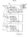
- The fourth example of Fig. 7 is a color image processing in which the gray-scale data Gg, Bg, and Rg of the color image data G, B, and R are respectively used. Fig. 7 illustrates the state of each unit when ASEL (4) is specified to the selectors 1041-1043 in the image data distribute
circuit 31 and the program specifications IFUN (1), ADLY (0), PEFUN (1), AUFUN (1), LUFUN (1), OUFUN (1, 0), and PEINH (1,2,2,2) are made to each ISP, hence the following operation is carried out:
RAM 302 of the ISP. This function is used to convert a color image into a monochrome image. It can be further applicable to the operations described below by changing PEFUN, AUFUN, and LUFUN. - Color image distance

- Maximum and minimum values of color image


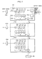
- The fifth example of Fig. 8 represents a binary-value pattern matching operation in which the binary data F60 to F67 of the gray-scale image data F are used. Fig. 8 depicts the state of each unit when ASEL (3) is specified for the selectors 1041-1043 of the image data distribute
circuit 31, the program specifications IFUN (1), PEFUN (13), AUFUN (1), LUFUN (1), OUFUN (1, 0), and PEINH (1, 1, 1, 1 ) are made to each ISP, and ADLY (0), ADLY (4), and ADLY (8) are specified for the ISP's 341, 342, and 343, respectively. In this case, the following operation is achieved.
- P12 represents a binary data of eight vertical pixels on the screen because the binary data Fb is delayed by one line to seven lines in the
delay circuit 102, while P11 to P, are obtained by delaying the binary data Fb by one pixel to 11 pixels. As a result, a binary image comprising 8 (vertical) by 12 (horizontal) pixels on the screen is stored as P12 to P, in theshift register 303, hence the pattern matching between these data items and the template signals tl2 to t, stored in theRAM 302 can be implemented. - Operations of the multifunctional image processor have been described by referring to the five examples; however, a variety of operations such as the gray-scale density conversion and arithmetic operation between a binary image and a gray-scale image can also be accomplished by use of the gray-scale image data and color image data each comprising gray-scale data and binary data.
- In accordance with the present invention, various kinds of data processing configurations and operation functions can be specified by use of programs, hence the present invention effectively enables a single image processor to execute many image processing functions at a higher speed.
- While the present invention has been described with reference to the particular illustrative embodiments, it is not to be restricted by those embodiments but only by the appended claims.
Claims (9)
characterised in that said image data distribute means (31) further includes
Applications Claiming Priority (2)
| Application Number | Priority Date | Filing Date | Title |
|---|---|---|---|
| JP6308/84 | 1984-01-19 | ||
| JP59006308A JPS60151789A (en) | 1984-01-19 | 1984-01-19 | Multifunctional processor of picture |
Publications (3)
| Publication Number | Publication Date |
|---|---|
| EP0150060A2 EP0150060A2 (en) | 1985-07-31 |
| EP0150060A3 EP0150060A3 (en) | 1986-07-30 |
| EP0150060B1 true EP0150060B1 (en) | 1990-09-19 |
Family
ID=11634742
Family Applications (1)
| Application Number | Title | Priority Date | Filing Date |
|---|---|---|---|
| EP85100507A Expired EP0150060B1 (en) | 1984-01-19 | 1985-01-18 | Multifunctional image processor |
Country Status (4)
| Country | Link |
|---|---|
| US (1) | US4718091A (en) |
| EP (1) | EP0150060B1 (en) |
| JP (1) | JPS60151789A (en) |
| DE (1) | DE3579705D1 (en) |
Cited By (7)
| Publication number | Priority date | Publication date | Assignee | Title |
|---|---|---|---|---|
| US6061749A (en) | 1997-04-30 | 2000-05-09 | Canon Kabushiki Kaisha | Transformation of a first dataword received from a FIFO into an input register and subsequent dataword from the FIFO into a normalized output dataword |
| US6118724A (en) | 1997-04-30 | 2000-09-12 | Canon Kabushiki Kaisha | Memory controller architecture |
| US6195674B1 (en) | 1997-04-30 | 2001-02-27 | Canon Kabushiki Kaisha | Fast DCT apparatus |
| US6237079B1 (en) | 1997-03-30 | 2001-05-22 | Canon Kabushiki Kaisha | Coprocessor interface having pending instructions queue and clean-up queue and dynamically allocating memory |
| US6311258B1 (en) | 1997-04-03 | 2001-10-30 | Canon Kabushiki Kaisha | Data buffer apparatus and method for storing graphical data using data encoders and decoders |
| US6336180B1 (en) | 1997-04-30 | 2002-01-01 | Canon Kabushiki Kaisha | Method, apparatus and system for managing virtual memory with virtual-physical mapping |
| US6707463B1 (en) | 1997-04-30 | 2004-03-16 | Canon Kabushiki Kaisha | Data normalization technique |
Families Citing this family (36)
| Publication number | Priority date | Publication date | Assignee | Title |
|---|---|---|---|---|
| US5274717A (en) * | 1985-02-01 | 1993-12-28 | Hitachi, Ltd. | Parallel image processor for performing local neighboring image processing |
| CA1283738C (en) * | 1985-11-13 | 1991-04-30 | Atsushi Hasebe | Data processor |
| US4791677A (en) * | 1985-12-16 | 1988-12-13 | Matsushita Electric Industrial Co., Ltd. | Image signal processor |
| US4845767A (en) * | 1985-12-16 | 1989-07-04 | Matsushita Electric Industrial Co., Ltd. | Image signal processor |
| US4752894A (en) * | 1985-12-30 | 1988-06-21 | Deering Michael F | Color plotter controller |
| JPS62195696A (en) * | 1986-02-21 | 1987-08-28 | 日本電気株式会社 | Display unit |
| US5276778A (en) * | 1987-01-08 | 1994-01-04 | Ezel, Inc. | Image processing system |
| DE274376T1 (en) * | 1987-01-08 | 1989-01-05 | Ezel Inc., Tokio/Tokyo, Jp | IMAGE PROCESSING SYSTEM. |
| US5163133A (en) * | 1987-02-17 | 1992-11-10 | Sam Technology, Inc. | Parallel processing system having a broadcast, result, and instruction bus for transmitting, receiving and controlling the computation of data |
| DE3804938C2 (en) * | 1987-02-18 | 1994-07-28 | Canon Kk | Image processing device |
| US4965750A (en) * | 1987-03-31 | 1990-10-23 | Hitachi, Ltd. | Graphic processor suitable for graphic data transfer and conversion processes |
| US4949390A (en) * | 1987-04-16 | 1990-08-14 | Applied Vision Systems, Inc. | Interconnect verification using serial neighborhood processors |
| US4829585A (en) * | 1987-05-04 | 1989-05-09 | Polaroid Corporation | Electronic image processing circuit |
| JPH01105998A (en) * | 1987-10-19 | 1989-04-24 | Ezel Inc | Video processing system |
| JPH01106092A (en) * | 1987-10-20 | 1989-04-24 | Ezel Inc | Video processing system |
| US5553170A (en) * | 1987-07-09 | 1996-09-03 | Ezel, Inc. | High speed image processing system having a preparation portion and a converting portion generating a processed image based on the preparation portion |
| US5136664A (en) * | 1988-02-23 | 1992-08-04 | Bersack Bret B | Pixel rendering |
| US5003613A (en) * | 1988-12-21 | 1991-03-26 | Recognition Equipment Incorporated | Document processing system and method |
| DE4027897C2 (en) * | 1989-09-05 | 1996-07-18 | Canon Kk | Image processing device |
| US5193126A (en) * | 1990-01-25 | 1993-03-09 | Toyo Ink Mfg. Co., Ltd. | Image deformation method and apparatus using coordinate transformation |
| JPH03232070A (en) * | 1990-02-08 | 1991-10-16 | Hitachi Ltd | Picture processor |
| GB2245795A (en) * | 1990-07-05 | 1992-01-08 | Rank Cintel Ltd | Generating convoluted digital video signals |
| JPH04116779A (en) * | 1990-09-07 | 1992-04-17 | Takayama:Kk | Data processor |
| US5151953A (en) * | 1990-12-10 | 1992-09-29 | Harris Corporation | Single chip 2-D convolver |
| EP0626661A1 (en) * | 1993-05-24 | 1994-11-30 | Societe D'applications Generales D'electricite Et De Mecanique Sagem | Digital image processing circuitry |
| JP3626514B2 (en) * | 1994-01-21 | 2005-03-09 | 株式会社ルネサステクノロジ | Image processing circuit |
| US5606707A (en) * | 1994-09-30 | 1997-02-25 | Martin Marietta Corporation | Real-time image processor |
| US6289138B1 (en) | 1997-04-30 | 2001-09-11 | Canon Kabushiki Kaisha | General image processor |
| EP0967792B1 (en) * | 1998-06-26 | 2011-08-03 | Sony Corporation | Printer having image correcting capability |
| DE19921418C2 (en) * | 1999-05-08 | 2002-09-19 | Agfa Gevaert Ag | Device for processing digital image data |
| US20040131276A1 (en) * | 2002-12-23 | 2004-07-08 | John Hudson | Region-based image processor |
| SE526060C2 (en) * | 2003-08-13 | 2005-06-28 | Elinnova Hb | Position detection device |
| JP2012253667A (en) * | 2011-06-06 | 2012-12-20 | Sony Corp | Image processing apparatus, image processing method, and program |
| US20180005059A1 (en) * | 2016-07-01 | 2018-01-04 | Google Inc. | Statistics Operations On Two Dimensional Image Processor |
| CN107801026B (en) * | 2017-11-09 | 2019-12-03 | 京东方科技集团股份有限公司 | Method for compressing image and device, compression of images and decompression systems |
| CN110930290B (en) * | 2019-11-13 | 2023-07-07 | 东软睿驰汽车技术(沈阳)有限公司 | Data processing method and device |
Family Cites Families (8)
| Publication number | Priority date | Publication date | Assignee | Title |
|---|---|---|---|---|
| US4322716A (en) * | 1976-11-15 | 1982-03-30 | Environmental Research Institute Of Michigan | Method and apparatus for pattern recognition and detection |
| US4266249A (en) * | 1978-09-19 | 1981-05-05 | Bell Telephone Laboratories, Incorporated | Digital encoder for facsimile transmission |
| US4319267A (en) * | 1979-02-16 | 1982-03-09 | Nippon Telegraph And Telephone Public Corporation | Picture coding and/or decoding equipment |
| US4464788A (en) * | 1979-09-10 | 1984-08-07 | Environmental Research Institute Of Michigan | Dynamic data correction generator for an image analyzer system |
| JPS56135262A (en) * | 1980-03-24 | 1981-10-22 | Nec Corp | Real-time signal processor on multiprocessor system |
| JPS6053349B2 (en) * | 1981-06-19 | 1985-11-25 | 株式会社日立製作所 | image processing processor |
| JPS5864577A (en) * | 1981-10-14 | 1983-04-16 | Yokogawa Hokushin Electric Corp | Shifting circuit for digital picture |
| JPS58181171A (en) * | 1982-04-16 | 1983-10-22 | Hitachi Ltd | Parallel picture processing processor |
-
1984
- 1984-01-19 JP JP59006308A patent/JPS60151789A/en active Pending
-
1985
- 1985-01-17 US US06/692,108 patent/US4718091A/en not_active Expired - Fee Related
- 1985-01-18 EP EP85100507A patent/EP0150060B1/en not_active Expired
- 1985-01-18 DE DE8585100507T patent/DE3579705D1/en not_active Expired - Lifetime
Cited By (15)
| Publication number | Priority date | Publication date | Assignee | Title |
|---|---|---|---|---|
| US6393545B1 (en) | 1919-04-30 | 2002-05-21 | Canon Kabushiki Kaisha | Method apparatus and system for managing virtual memory with virtual-physical mapping |
| US6237079B1 (en) | 1997-03-30 | 2001-05-22 | Canon Kabushiki Kaisha | Coprocessor interface having pending instructions queue and clean-up queue and dynamically allocating memory |
| US6311258B1 (en) | 1997-04-03 | 2001-10-30 | Canon Kabushiki Kaisha | Data buffer apparatus and method for storing graphical data using data encoders and decoders |
| US6272257B1 (en) | 1997-04-30 | 2001-08-07 | Canon Kabushiki Kaisha | Decoder of variable length codes |
| US6246396B1 (en) | 1997-04-30 | 2001-06-12 | Canon Kabushiki Kaisha | Cached color conversion method and apparatus |
| US6259456B1 (en) | 1997-04-30 | 2001-07-10 | Canon Kabushiki Kaisha | Data normalization techniques |
| US6061749A (en) | 1997-04-30 | 2000-05-09 | Canon Kabushiki Kaisha | Transformation of a first dataword received from a FIFO into an input register and subsequent dataword from the FIFO into a normalized output dataword |
| US6195674B1 (en) | 1997-04-30 | 2001-02-27 | Canon Kabushiki Kaisha | Fast DCT apparatus |
| US6336180B1 (en) | 1997-04-30 | 2002-01-01 | Canon Kabushiki Kaisha | Method, apparatus and system for managing virtual memory with virtual-physical mapping |
| US6349379B2 (en) | 1997-04-30 | 2002-02-19 | Canon Kabushiki Kaisha | System for executing instructions having flag for indicating direct or indirect specification of a length of operand data |
| US6118724A (en) | 1997-04-30 | 2000-09-12 | Canon Kabushiki Kaisha | Memory controller architecture |
| US6414687B1 (en) | 1997-04-30 | 2002-07-02 | Canon Kabushiki Kaisha | Register setting-micro programming system |
| US6507898B1 (en) | 1997-04-30 | 2003-01-14 | Canon Kabushiki Kaisha | Reconfigurable data cache controller |
| US6674536B2 (en) | 1997-04-30 | 2004-01-06 | Canon Kabushiki Kaisha | Multi-instruction stream processor |
| US6707463B1 (en) | 1997-04-30 | 2004-03-16 | Canon Kabushiki Kaisha | Data normalization technique |
Also Published As
| Publication number | Publication date |
|---|---|
| EP0150060A2 (en) | 1985-07-31 |
| EP0150060A3 (en) | 1986-07-30 |
| JPS60151789A (en) | 1985-08-09 |
| US4718091A (en) | 1988-01-05 |
| DE3579705D1 (en) | 1990-10-25 |
Similar Documents
| Publication | Publication Date | Title |
|---|---|---|
| EP0150060B1 (en) | Multifunctional image processor | |
| US5608824A (en) | Image processing apparatus in which filters having different filtering characteristics can be switched among themselves | |
| US9202292B2 (en) | Image processing apparatus having a plurality of image processing blocks that are capable of real-time processing of an image signal | |
| US4213150A (en) | Real-time edge processing unit | |
| EP0743617B1 (en) | Image processing method and apparatus thereof | |
| US5678033A (en) | Multi-stage interpolation processor | |
| EP3553709A1 (en) | Deep learning image processing systems using modularly connected cnn based integrated circuits | |
| US5031037A (en) | Method and apparatus for vector quantizer parallel processing | |
| EP0069542B1 (en) | Data processing arrangement | |
| US4736440A (en) | Process for the processing of digitized signals representing an original image | |
| US5946222A (en) | Method and apparatus for performing a masked byte addition operation | |
| US5715436A (en) | Image processing LSI circuit with image preprocessing, feature extraction and matching | |
| EP0316956B1 (en) | Image processing system | |
| US5781667A (en) | Apparatus for high speed morphological processing | |
| EP0189943B1 (en) | Parallel image processor | |
| US7663631B1 (en) | Pixel engine architecture | |
| US7171059B1 (en) | Method and apparatus for two-dimensional image scaling | |
| CN106296614B (en) | Image processing apparatus and image processing method | |
| US5333263A (en) | Digital image processing apparatus | |
| JPH04100179A (en) | Image processor | |
| KR930000997B1 (en) | Processing method for image arrangement | |
| US4987557A (en) | System for calculation of sum of products by repetitive input of data | |
| JPS6280775A (en) | Image processor | |
| JP3442953B2 (en) | Clipping equipment | |
| JP2623089B2 (en) | Video processing system |
Legal Events
| Date | Code | Title | Description |
|---|---|---|---|
| PUAI | Public reference made under article 153(3) epc to a published international application that has entered the european phase |
Free format text: ORIGINAL CODE: 0009012 |
|
| AK | Designated contracting states |
Designated state(s): CH DE FR GB IT LI NL SE |
|
| PUAL | Search report despatched |
Free format text: ORIGINAL CODE: 0009013 |
|
| AK | Designated contracting states |
Kind code of ref document: A3 Designated state(s): CH DE FR GB IT LI NL SE |
|
| 17P | Request for examination filed |
Effective date: 19861128 |
|
| 17Q | First examination report despatched |
Effective date: 19881004 |
|
| GRAA | (expected) grant |
Free format text: ORIGINAL CODE: 0009210 |
|
| AK | Designated contracting states |
Kind code of ref document: B1 Designated state(s): CH DE FR GB IT LI NL SE |
|
| REF | Corresponds to: |
Ref document number: 3579705 Country of ref document: DE Date of ref document: 19901025 |
|
| ET | Fr: translation filed | ||
| ITF | It: translation for a ep patent filed |
Owner name: MODIANO & ASSOCIATI S.R.L. |
|
| ITTA | It: last paid annual fee | ||
| PLBE | No opposition filed within time limit |
Free format text: ORIGINAL CODE: 0009261 |
|
| STAA | Information on the status of an ep patent application or granted ep patent |
Free format text: STATUS: NO OPPOSITION FILED WITHIN TIME LIMIT |
|
| 26N | No opposition filed | ||
| PGFP | Annual fee paid to national office [announced via postgrant information from national office to epo] |
Ref country code: CH Payment date: 19920326 Year of fee payment: 8 |
|
| PG25 | Lapsed in a contracting state [announced via postgrant information from national office to epo] |
Ref country code: LI Effective date: 19930131 Ref country code: CH Effective date: 19930131 |
|
| REG | Reference to a national code |
Ref country code: CH Ref legal event code: PL |
|
| PGFP | Annual fee paid to national office [announced via postgrant information from national office to epo] |
Ref country code: FR Payment date: 19931129 Year of fee payment: 10 |
|
| PGFP | Annual fee paid to national office [announced via postgrant information from national office to epo] |
Ref country code: SE Payment date: 19931130 Year of fee payment: 10 |
|
| PGFP | Annual fee paid to national office [announced via postgrant information from national office to epo] |
Ref country code: GB Payment date: 19940107 Year of fee payment: 10 |
|
| PGFP | Annual fee paid to national office [announced via postgrant information from national office to epo] |
Ref country code: NL Payment date: 19940131 Year of fee payment: 10 |
|
| PGFP | Annual fee paid to national office [announced via postgrant information from national office to epo] |
Ref country code: DE Payment date: 19940328 Year of fee payment: 10 |
|
| PG25 | Lapsed in a contracting state [announced via postgrant information from national office to epo] |
Ref country code: GB Effective date: 19950118 |
|
| PG25 | Lapsed in a contracting state [announced via postgrant information from national office to epo] |
Ref country code: SE Effective date: 19950119 |
|
| EAL | Se: european patent in force in sweden |
Ref document number: 85100507.4 |
|
| PG25 | Lapsed in a contracting state [announced via postgrant information from national office to epo] |
Ref country code: NL Effective date: 19950801 |
|
| GBPC | Gb: european patent ceased through non-payment of renewal fee |
Effective date: 19950118 |
|
| PG25 | Lapsed in a contracting state [announced via postgrant information from national office to epo] |
Ref country code: FR Effective date: 19950929 |
|
| NLV4 | Nl: lapsed or anulled due to non-payment of the annual fee |
Effective date: 19950801 |
|
| PG25 | Lapsed in a contracting state [announced via postgrant information from national office to epo] |
Ref country code: DE Effective date: 19951003 |
|
| EUG | Se: european patent has lapsed |
Ref document number: 85100507.4 |
|
| REG | Reference to a national code |
Ref country code: FR Ref legal event code: ST |