EP0157482A2 - Surface acoustic wave device - Google Patents
Surface acoustic wave device Download PDFInfo
- Publication number
- EP0157482A2 EP0157482A2 EP85301073A EP85301073A EP0157482A2 EP 0157482 A2 EP0157482 A2 EP 0157482A2 EP 85301073 A EP85301073 A EP 85301073A EP 85301073 A EP85301073 A EP 85301073A EP 0157482 A2 EP0157482 A2 EP 0157482A2
- Authority
- EP
- European Patent Office
- Prior art keywords
- surface acoustic
- acoustic wave
- substrate
- transducer means
- output
- Prior art date
- Legal status (The legal status is an assumption and is not a legal conclusion. Google has not performed a legal analysis and makes no representation as to the accuracy of the status listed.)
- Granted
Links
Images
Classifications
-
- H—ELECTRICITY
- H03—ELECTRONIC CIRCUITRY
- H03H—IMPEDANCE NETWORKS, e.g. RESONANT CIRCUITS; RESONATORS
- H03H9/00—Networks comprising electromechanical or electro-acoustic devices; Electromechanical resonators
- H03H9/30—Time-delay networks
- H03H9/42—Time-delay networks using surface acoustic waves
-
- H—ELECTRICITY
- H03—ELECTRONIC CIRCUITRY
- H03H—IMPEDANCE NETWORKS, e.g. RESONANT CIRCUITS; RESONATORS
- H03H9/00—Networks comprising electromechanical or electro-acoustic devices; Electromechanical resonators
- H03H9/74—Multiple-port networks for connecting several sources or loads, working on the same frequency or frequency band, to a common load or source
- H03H9/76—Networks using surface acoustic waves
Definitions
- a signal delayed by t X may still be received, albeit of reduced amplitude, on account of reflections occurring at the output transducers and, in general, this will bappen whenever the total path length due to reflections corresponds to the elapsed time t .
- a wave received at the output transducer T 04 may be subject to a delay t on account of a reflection occurring at output transducer T 05 .
- a substrate 10 is provided, at a major surface, with an input transducer arrangement T arranged to launch a relatively broad wave along a fixed, propagation direction P.
- the wavefront thus presented is shown at AA'.
- the output transducers need not necessarily be arranged along parallel tracks, in side-by-side relationship, as shown in Figure 3.
- the input transducer may be positioned centrally on the substrate, the output transducers being arranged in their respective tracks 20, 30 on opposite sides of the input transducer, but with the same relative spacings.
Abstract
Description
- This invention relates to a surface acoustic wave device and it relates especially to such a device suitable for subjecting a surface acoustic wave (SAW) to a number of different delays.
- A surface acoustic wave device typically comprises a substrate of a piezoelectric material, e.g. quartz lead zirconate ceramic (PZT) or lithium niobate (LiNb03), which is provided, at one of its major surfaces, with an input transducer for launching a SAW along a suitable cystallographic direction and an output transducer for receiving the wave, after a delay due to the propagation time. Usually, the input and output transducers are in the form of interdigital arrays of strip electrodes applied to the substrate by a suitable photolithographic technique.
- The value of a device of this kind lies in the fact that the velocity of a SAW propagating at the surface of a piezoelectric substrate is much smaller than that of an electromagnetic wave used to excite the input transducer; thus relatively large delays can be achieved.
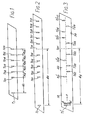
- It may be desirable in practice to subject a SAW to different delays and to this end a plurality of output transducers is arranged on the substrate, individual transducers being spaced apart along the propagation direction. A device of this kind is shown, by way of example, in Figure 1; the input transducer is represented at TI and six output transducers are represented at T01, T02 ... T06.
- A wave launched by the input transducer is received at, the output transducers T01, T02 .... T06 after respective delays ts; ts+t12; .... ts+t12+ t 23 +t34 +t45 +t56 where ts is the elapsed time due to propagation of the wave over a distance ds separating the input transducer and the nearest ouput transducer T01, and t12; t 23 .... t56 are the elapsed times due to propagation of the wave over distances d12, d23 .... d56 separating respective pairs of adjacent output transducers.
- A wave may suffer a partial reflection at an output transducer and, in these circumstances, transducer T01, for example, may receive a wave after a delay ts+2t12 due to a reflection occurring at transducer T02. If, as is commonly the case, the output transducers are spaced apart at regular intervals on the substrate such that t12 = t 23 = .... t 56 a wave may be received simultaneously at different output transducers. For example, a wave received at transducers T01 and T03 may be subject to the same delay t' = ts+2t12 = ts+t12+t23.
- In some signal processing applications it is desirable to arrange that a surface acoustic wave device be capable of rejecting a wave which has been subjected to a specific (undesirable) delay. Hitherto, it has been customary to omit one of the output transducers. As shown in Figure 2 of the accompanying drawings, an output transducer which would otherwise occupy a position referenced at T0X, intermediate transducers T05 and T06, has been omitted - thus a wave delayed by an amount tx, the elapsed time due to propagation of the wave directly over a distance d on the substrate, as shown, remains undetected.
- In practice, however, a signal delayed by tX may still be received, albeit of reduced amplitude, on account of reflections occurring at the output transducers and, in general, this will bappen whenever the total path length due to reflections corresponds to the elapsed time t . Thus, for example, a wave received at the output transducer T04 may be subject to a delay t on account of a reflection occurring at output transducer T 05.
- It is an object of the present invention to provide a surface acoustic wave device wherein the above-mentioned problem is substantially alleviated.
- Accordingly there is provided a surface acoustic wave device wherein a substrate of a piezoelectric material is provided with input transducer means for launching a surface acoustic wave in a fixed, propagation direction and a plurality of output transducers means: spaced apart along said fixed propagation direction to receive a surface acoustic wave so launched wherein some of said output transducer means are arranged on a first track on the substrate and others of said output transducer means are arranged on a different track on the substrate, whereby a surface acoustic wave received at said output transducer means is subjected to respective delays excluding one or more delays which would have resulted if the output transducer means had been arranged along said fixed, propagation direction with the same spacings relative to said input transducer means, but on a single track only.
- In a preferred embodiment the first and different tracks are on the same side of said input transducer means.
- In order that the invention may be carried into effect an embodiment thereof is now described, by way of example only, by reference to Figure 3 of the accompanying drawings which shows a perspective view of a surface acoustic wave device.
- Referring now to Figure 3, a
substrate 10 is provided, at a major surface, with an input transducer arrangement T arranged to launch a relatively broad wave along a fixed, propagation direction P. The wavefront thus presented is shown at AA'. - In this example the output transducers T01', T02' .... T0'10 are arranged at regular intervals along the propagation direction, except for an interruption at the position referenced Ty where a transducer has been omitted. With this arrangement, a wave delayed by an amount ty the elapsed time due to propagation of a wave directly from the input transducer to position Ty remains undetected.
- Moreover, the output transducers are arranged on the substrate on two distinct tracks, in side-by-side relationship. Transducers T01, T04, T07, T08 and T010 are arranged on a first track, indicated generally at 20, and transducers T02, T03, T05, T06 and T 09 are arranged on a second track, parallel to the first, indicated generally at 30.
- As will be apparent from the drawing, the relative spacings of the transducers in each track is such that it is not possible to construct a path length, from the input transducer to any one of the output transducers, corresponding to the delay t - even taking into account reflections occurring at the output transducer. Thus, in constrast to the device described hereinbefore by reference to Figure 2 wherein the transducers are arranged on a single track only, any significant wave, delayed by an amount ty, remains undetected.
- It will be appreciated that the output transducers need not necessarily be arranged along parallel tracks, in side-by-side relationship, as shown in Figure 3. In an alternative embodiment the input transducer may be positioned centrally on the substrate, the output transducers being arranged in their
respective tracks 20, 30 on opposite sides of the input transducer, but with the same relative spacings.
Claims (3)
Applications Claiming Priority (2)
| Application Number | Priority Date | Filing Date | Title |
|---|---|---|---|
| GB8408168 | 1984-03-29 | ||
| GB848408168A GB8408168D0 (en) | 1984-03-29 | 1984-03-29 | Surface acoustic wave device |
Publications (3)
| Publication Number | Publication Date |
|---|---|
| EP0157482A2 true EP0157482A2 (en) | 1985-10-09 |
| EP0157482A3 EP0157482A3 (en) | 1987-04-01 |
| EP0157482B1 EP0157482B1 (en) | 1991-05-15 |
Family
ID=10558889
Family Applications (1)
| Application Number | Title | Priority Date | Filing Date |
|---|---|---|---|
| EP19850301073 Expired EP0157482B1 (en) | 1984-03-29 | 1985-02-19 | Surface acoustic wave device |
Country Status (3)
| Country | Link |
|---|---|
| EP (1) | EP0157482B1 (en) |
| DE (1) | DE3582814D1 (en) |
| GB (1) | GB8408168D0 (en) |
Citations (3)
| Publication number | Priority date | Publication date | Assignee | Title |
|---|---|---|---|---|
| US3715674A (en) * | 1971-07-23 | 1973-02-06 | Stanford Research Inst | Electrically controlled reflection of acoustic surface waves |
| US3873946A (en) * | 1973-10-04 | 1975-03-25 | Hughes Aircraft Co | Acoustic surface wave tapped delay line |
| JPS5431252A (en) * | 1977-08-12 | 1979-03-08 | Matsushita Electric Ind Co Ltd | Solid state delay line device |
-
1984
- 1984-03-29 GB GB848408168A patent/GB8408168D0/en active Pending
-
1985
- 1985-02-19 EP EP19850301073 patent/EP0157482B1/en not_active Expired
- 1985-02-19 DE DE8585301073T patent/DE3582814D1/en not_active Expired - Lifetime
Patent Citations (3)
| Publication number | Priority date | Publication date | Assignee | Title |
|---|---|---|---|---|
| US3715674A (en) * | 1971-07-23 | 1973-02-06 | Stanford Research Inst | Electrically controlled reflection of acoustic surface waves |
| US3873946A (en) * | 1973-10-04 | 1975-03-25 | Hughes Aircraft Co | Acoustic surface wave tapped delay line |
| JPS5431252A (en) * | 1977-08-12 | 1979-03-08 | Matsushita Electric Ind Co Ltd | Solid state delay line device |
Non-Patent Citations (2)
| Title |
|---|
| PATENTS ABSTRACTS OF JAPAN, vol. 3, no. 52 (E-108), 7th May 1979, page 104 E108; & JP-A-54 031 252 (MATSUSHITA DENKI SANGYO K.K.) 08-03-1979 * |
| THE TRANSACTIONS OF THE IECE OF JAPAN, vol. E62, no. 11, November 1979, pages 775-778, Tokyo, JP; J. TEMMYO et al.: "A new tapping design for low-distortion SAW tapped delay lines" * |
Also Published As
| Publication number | Publication date |
|---|---|
| EP0157482A3 (en) | 1987-04-01 |
| DE3582814D1 (en) | 1991-06-20 |
| EP0157482B1 (en) | 1991-05-15 |
| GB8408168D0 (en) | 1984-05-10 |
Similar Documents
| Publication | Publication Date | Title |
|---|---|---|
| US5717434A (en) | Ultrasonic touch system | |
| US3810257A (en) | Acoustic surface wave transducer configuration for reducing triple transit signals | |
| US4598224A (en) | Surface acoustic wave device for sensing the presence of chemical agents | |
| KR960016121A (en) | Surface acoustic wave filter | |
| US4388600A (en) | Surface acoustic wave device | |
| NL7907049A (en) | SOUND WAVE DEVICE. | |
| EP0924857A3 (en) | Surface acoustic wave filter | |
| EP0219182A3 (en) | Staggered saw resonator differential detection | |
| US4055820A (en) | Reflective dot array for acoustic wave processing | |
| US3399314A (en) | Ultrasonic signal apparatus | |
| US4814658A (en) | SAW device with continuous finger pattern | |
| US4096455A (en) | Surface wave termination for saw device | |
| US4350963A (en) | Surface acoustic wave device | |
| US4604595A (en) | Surface acoustic wave device having interdigitated comb electrodes weighted for odd/even response | |
| US3878407A (en) | Surface wave electromechanical filter | |
| JPH0351327B2 (en) | ||
| GB1413916A (en) | Acoustic surface-wave devices | |
| EP0157482A2 (en) | Surface acoustic wave device | |
| US3621309A (en) | Electric-mechanical transducer | |
| US3815056A (en) | Continuous surface wave device | |
| US4330728A (en) | Surface acoustic wave coupling with respect to non-piezoelectric substrates | |
| GB1357193A (en) | Acoustic surface wave devices | |
| US3873946A (en) | Acoustic surface wave tapped delay line | |
| EP0197640A2 (en) | Saw devices with reflection-suppressing fingers | |
| US5471179A (en) | Surface acoustic wave bandpass filter including unique V-shaped electrode and phase compensator |
Legal Events
| Date | Code | Title | Description |
|---|---|---|---|
| PUAI | Public reference made under article 153(3) epc to a published international application that has entered the european phase |
Free format text: ORIGINAL CODE: 0009012 |
|
| AK | Designated contracting states |
Designated state(s): DE FR GB |
|
| PUAL | Search report despatched |
Free format text: ORIGINAL CODE: 0009013 |
|
| AK | Designated contracting states |
Kind code of ref document: A3 Designated state(s): DE FR GB |
|
| 17P | Request for examination filed |
Effective date: 19870629 |
|
| 17Q | First examination report despatched |
Effective date: 19890104 |
|
| GRAA | (expected) grant |
Free format text: ORIGINAL CODE: 0009210 |
|
| AK | Designated contracting states |
Kind code of ref document: B1 Designated state(s): DE FR GB |
|
| REF | Corresponds to: |
Ref document number: 3582814 Country of ref document: DE Date of ref document: 19910620 |
|
| ET | Fr: translation filed | ||
| PLBE | No opposition filed within time limit |
Free format text: ORIGINAL CODE: 0009261 |
|
| STAA | Information on the status of an ep patent application or granted ep patent |
Free format text: STATUS: NO OPPOSITION FILED WITHIN TIME LIMIT |
|
| 26N | No opposition filed | ||
| PGFP | Annual fee paid to national office [announced via postgrant information from national office to epo] |
Ref country code: DE Payment date: 19950222 Year of fee payment: 11 |
|
| PGFP | Annual fee paid to national office [announced via postgrant information from national office to epo] |
Ref country code: FR Payment date: 19960125 Year of fee payment: 12 |
|
| PGFP | Annual fee paid to national office [announced via postgrant information from national office to epo] |
Ref country code: GB Payment date: 19960212 Year of fee payment: 12 |
|
| PG25 | Lapsed in a contracting state [announced via postgrant information from national office to epo] |
Ref country code: DE Effective date: 19961101 |
|
| REG | Reference to a national code |
Ref country code: GB Ref legal event code: 732E |
|
| PG25 | Lapsed in a contracting state [announced via postgrant information from national office to epo] |
Ref country code: GB Effective date: 19970219 |
|
| GBPC | Gb: european patent ceased through non-payment of renewal fee |
Effective date: 19970219 |
|
| PG25 | Lapsed in a contracting state [announced via postgrant information from national office to epo] |
Ref country code: FR Effective date: 19971030 |
|
| REG | Reference to a national code |
Ref country code: FR Ref legal event code: ST |